EP3182478A1 - Electron injection layer for an organic light-emitting diode (oled) - Google Patents
Electron injection layer for an organic light-emitting diode (oled) Download PDFInfo
- Publication number
- EP3182478A1 EP3182478A1 EP15201418.9A EP15201418A EP3182478A1 EP 3182478 A1 EP3182478 A1 EP 3182478A1 EP 15201418 A EP15201418 A EP 15201418A EP 3182478 A1 EP3182478 A1 EP 3182478A1
- Authority
- EP
- European Patent Office
- Prior art keywords
- layer
- substituted
- cathode electrode
- metal
- group
- Prior art date
- Legal status (The legal status is an assumption and is not a legal conclusion. Google has not performed a legal analysis and makes no representation as to the accuracy of the status listed.)
- Granted
Links
- 238000002347 injection Methods 0.000 title claims abstract description 183
- 239000007924 injection Substances 0.000 title claims abstract description 183
- -1 phosphine compound Chemical class 0.000 claims abstract description 192
- 229910052751 metal Inorganic materials 0.000 claims abstract description 161
- 239000002184 metal Substances 0.000 claims abstract description 159
- XYFCBTPGUUZFHI-UHFFFAOYSA-N Phosphine Natural products P XYFCBTPGUUZFHI-UHFFFAOYSA-N 0.000 claims abstract description 72
- 229910000073 phosphorus hydride Inorganic materials 0.000 claims abstract description 71
- 229910052723 transition metal Inorganic materials 0.000 claims abstract description 27
- 150000003624 transition metals Chemical class 0.000 claims abstract description 27
- 150000003839 salts Chemical class 0.000 claims abstract description 22
- 229910052761 rare earth metal Inorganic materials 0.000 claims abstract description 20
- 150000002910 rare earth metals Chemical class 0.000 claims abstract description 20
- 229910052784 alkaline earth metal Inorganic materials 0.000 claims abstract description 19
- 229910052783 alkali metal Inorganic materials 0.000 claims abstract description 18
- 150000001340 alkali metals Chemical class 0.000 claims abstract description 18
- 150000001342 alkaline earth metals Chemical class 0.000 claims abstract description 17
- 150000004696 coordination complex Chemical class 0.000 claims abstract description 16
- 150000002902 organometallic compounds Chemical class 0.000 claims abstract description 16
- 150000001875 compounds Chemical class 0.000 claims description 198
- 239000011159 matrix material Substances 0.000 claims description 114
- 230000000903 blocking effect Effects 0.000 claims description 64
- 125000003118 aryl group Chemical group 0.000 claims description 38
- 125000006539 C12 alkyl group Chemical group [H]C([H])([H])C([H])([H])C([H])([H])C([H])([H])C([H])([H])C([H])([H])C([H])([H])C([H])([H])C([H])([H])C([H])([H])C([H])([H])C([H])([H])* 0.000 claims description 35
- 125000001997 phenyl group Chemical group [H]C1=C([H])C([H])=C(*)C([H])=C1[H] 0.000 claims description 35
- 230000005525 hole transport Effects 0.000 claims description 34
- 239000000758 substrate Substances 0.000 claims description 32
- 125000000732 arylene group Chemical group 0.000 claims description 29
- 125000001072 heteroaryl group Chemical group 0.000 claims description 28
- 125000005549 heteroarylene group Chemical group 0.000 claims description 28
- 229910052782 aluminium Inorganic materials 0.000 claims description 27
- 229910052744 lithium Inorganic materials 0.000 claims description 21
- 239000000203 mixture Substances 0.000 claims description 20
- 229910052760 oxygen Inorganic materials 0.000 claims description 20
- 229910052717 sulfur Inorganic materials 0.000 claims description 19
- 229910052709 silver Inorganic materials 0.000 claims description 18
- 125000001624 naphthyl group Chemical group 0.000 claims description 17
- 125000004437 phosphorous atom Chemical group 0.000 claims description 15
- 229910052711 selenium Inorganic materials 0.000 claims description 15
- 238000004519 manufacturing process Methods 0.000 claims description 13
- 239000000956 alloy Substances 0.000 claims description 11
- 229910045601 alloy Inorganic materials 0.000 claims description 11
- MWPLVEDNUUSJAV-UHFFFAOYSA-N anthracene Chemical compound C1=CC=CC2=CC3=CC=CC=C3C=C21 MWPLVEDNUUSJAV-UHFFFAOYSA-N 0.000 claims description 11
- ZUOUZKKEUPVFJK-UHFFFAOYSA-N diphenyl Chemical compound C1=CC=CC=C1C1=CC=CC=C1 ZUOUZKKEUPVFJK-UHFFFAOYSA-N 0.000 claims description 11
- 229910052737 gold Inorganic materials 0.000 claims description 11
- OAPPEBNXKAKQGS-UHFFFAOYSA-N Benz[c]acridine Chemical compound C1=CC=C2C3=NC4=CC=CC=C4C=C3C=CC2=C1 OAPPEBNXKAKQGS-UHFFFAOYSA-N 0.000 claims description 10
- 125000000217 alkyl group Chemical group 0.000 claims description 10
- HAXBIWFMXWRORI-UHFFFAOYSA-N Benzo[k]fluoranthene Chemical compound C1=CC(C2=CC3=CC=CC=C3C=C22)=C3C2=CC=CC3=C1 HAXBIWFMXWRORI-UHFFFAOYSA-N 0.000 claims description 9
- 229910052791 calcium Inorganic materials 0.000 claims description 9
- 229910052802 copper Inorganic materials 0.000 claims description 9
- 125000003983 fluorenyl group Chemical group C1(=CC=CC=2C3=CC=CC=C3CC12)* 0.000 claims description 9
- 125000000843 phenylene group Chemical group C1(=C(C=CC=C1)*)* 0.000 claims description 9
- 125000004076 pyridyl group Chemical group 0.000 claims description 9
- 239000011701 zinc Substances 0.000 claims description 9
- OICJTSLHQGDCTQ-UHFFFAOYSA-N [1]benzothiolo[3,2-d]pyrimidine Chemical compound N1=CN=C2C3=CC=CC=C3SC2=C1 OICJTSLHQGDCTQ-UHFFFAOYSA-N 0.000 claims description 8
- WZJYKHNJTSNBHV-UHFFFAOYSA-N benzo[h]quinoline Chemical compound C1=CN=C2C3=CC=CC=C3C=CC2=C1 WZJYKHNJTSNBHV-UHFFFAOYSA-N 0.000 claims description 8
- 125000004404 heteroalkyl group Chemical group 0.000 claims description 8
- 229910052749 magnesium Inorganic materials 0.000 claims description 8
- 229910001507 metal halide Inorganic materials 0.000 claims description 8
- 150000005309 metal halides Chemical class 0.000 claims description 8
- 125000001725 pyrenyl group Chemical group 0.000 claims description 8
- 229910052725 zinc Inorganic materials 0.000 claims description 8
- SMWDFEZZVXVKRB-UHFFFAOYSA-N Quinoline Chemical compound N1=CC=CC2=CC=CC=C21 SMWDFEZZVXVKRB-UHFFFAOYSA-N 0.000 claims description 7
- XLOMVQKBTHCTTD-UHFFFAOYSA-N Zinc monoxide Chemical compound [Zn]=O XLOMVQKBTHCTTD-UHFFFAOYSA-N 0.000 claims description 7
- VPUGDVKSAQVFFS-UHFFFAOYSA-N coronene Chemical compound C1=C(C2=C34)C=CC3=CC=C(C=C3)C4=C4C3=CC=C(C=C3)C4=C2C3=C1 VPUGDVKSAQVFFS-UHFFFAOYSA-N 0.000 claims description 7
- 229910052733 gallium Inorganic materials 0.000 claims description 7
- 125000002496 methyl group Chemical group [H]C([H])([H])* 0.000 claims description 7
- BBEAQIROQSPTKN-UHFFFAOYSA-N pyrene Chemical compound C1=CC=C2C=CC3=CC=CC4=CC=C1C2=C43 BBEAQIROQSPTKN-UHFFFAOYSA-N 0.000 claims description 7
- UJOBWOGCFQCDNV-UHFFFAOYSA-N 9H-carbazole Chemical compound C1=CC=C2C3=CC=CC=C3NC2=C1 UJOBWOGCFQCDNV-UHFFFAOYSA-N 0.000 claims description 6
- ANUCHZVCBDOPOX-UHFFFAOYSA-N Dibenz[a,j]acridine Chemical compound C1=CC=CC2=C(C=C3C4=CC=CC=C4C=CC3=N3)C3=CC=C21 ANUCHZVCBDOPOX-UHFFFAOYSA-N 0.000 claims description 6
- JUJWROOIHBZHMG-UHFFFAOYSA-N Pyridine Chemical compound C1=CC=NC=C1 JUJWROOIHBZHMG-UHFFFAOYSA-N 0.000 claims description 6
- DZBUGLKDJFMEHC-UHFFFAOYSA-N acridine Chemical compound C1=CC=CC2=CC3=CC=CC=C3N=C21 DZBUGLKDJFMEHC-UHFFFAOYSA-N 0.000 claims description 6
- 239000004305 biphenyl Substances 0.000 claims description 6
- HKNRNTYTYUWGLN-UHFFFAOYSA-N dithieno[3,2-a:2',3'-d]thiophene Chemical compound C1=CSC2=C1SC1=C2C=CS1 HKNRNTYTYUWGLN-UHFFFAOYSA-N 0.000 claims description 6
- NIHNNTQXNPWCJQ-UHFFFAOYSA-N fluorene Chemical compound C1=CC=C2CC3=CC=CC=C3C2=C1 NIHNNTQXNPWCJQ-UHFFFAOYSA-N 0.000 claims description 6
- 125000005567 fluorenylene group Chemical group 0.000 claims description 6
- 229910052738 indium Inorganic materials 0.000 claims description 6
- YNPNZTXNASCQKK-UHFFFAOYSA-N phenanthrene Chemical compound C1=CC=C2C3=CC=CC=C3C=CC2=C1 YNPNZTXNASCQKK-UHFFFAOYSA-N 0.000 claims description 6
- 229910052708 sodium Inorganic materials 0.000 claims description 6
- JYEUMXHLPRZUAT-UHFFFAOYSA-N 1,2,3-triazine Chemical compound C1=CN=NN=C1 JYEUMXHLPRZUAT-UHFFFAOYSA-N 0.000 claims description 5
- YJTKZCDBKVTVBY-UHFFFAOYSA-N 1,3-Diphenylbenzene Chemical group C1=CC=CC=C1C1=CC=CC(C=2C=CC=CC=2)=C1 YJTKZCDBKVTVBY-UHFFFAOYSA-N 0.000 claims description 5
- 229910052788 barium Inorganic materials 0.000 claims description 5
- PQIUGRLKNKSKTC-UHFFFAOYSA-N benzo[h]quinazoline Chemical compound N1=CN=C2C3=CC=CC=C3C=CC2=C1 PQIUGRLKNKSKTC-UHFFFAOYSA-N 0.000 claims description 5
- 235000010290 biphenyl Nutrition 0.000 claims description 5
- UORVGPXVDQYIDP-UHFFFAOYSA-N borane Chemical compound B UORVGPXVDQYIDP-UHFFFAOYSA-N 0.000 claims description 5
- 229910052792 caesium Inorganic materials 0.000 claims description 5
- BTVBCAKHMZHLFR-UHFFFAOYSA-N dibenz[c,h]acridine Chemical compound C1=CC=CC2=C(N=C3C4=CC=CC=C4C=CC3=C3)C3=CC=C21 BTVBCAKHMZHLFR-UHFFFAOYSA-N 0.000 claims description 5
- 229910052742 iron Inorganic materials 0.000 claims description 5
- 125000004957 naphthylene group Chemical group 0.000 claims description 5
- 125000002080 perylenyl group Chemical group C1(=CC=C2C=CC=C3C4=CC=CC5=CC=CC(C1=C23)=C45)* 0.000 claims description 5
- 125000005561 phenanthryl group Chemical group 0.000 claims description 5
- 229910052700 potassium Inorganic materials 0.000 claims description 5
- XEJJWKBPMCMSJA-UHFFFAOYSA-N pyrido[3,2-h]quinazoline Chemical compound N1=CN=C2C3=NC=CC=C3C=CC2=C1 XEJJWKBPMCMSJA-UHFFFAOYSA-N 0.000 claims description 5
- 229910052712 strontium Inorganic materials 0.000 claims description 5
- MDDUHVRJJAFRAU-YZNNVMRBSA-N tert-butyl-[(1r,3s,5z)-3-[tert-butyl(dimethyl)silyl]oxy-5-(2-diphenylphosphorylethylidene)-4-methylidenecyclohexyl]oxy-dimethylsilane Chemical compound C1[C@@H](O[Si](C)(C)C(C)(C)C)C[C@H](O[Si](C)(C)C(C)(C)C)C(=C)\C1=C/CP(=O)(C=1C=CC=CC=1)C1=CC=CC=C1 MDDUHVRJJAFRAU-YZNNVMRBSA-N 0.000 claims description 5
- 125000005580 triphenylene group Chemical group 0.000 claims description 5
- BCMCBBGGLRIHSE-UHFFFAOYSA-N 1,3-benzoxazole Chemical compound C1=CC=C2OC=NC2=C1 BCMCBBGGLRIHSE-UHFFFAOYSA-N 0.000 claims description 4
- DJMUYABFXCIYSC-UHFFFAOYSA-N 1H-phosphole Chemical compound C=1C=CPC=1 DJMUYABFXCIYSC-UHFFFAOYSA-N 0.000 claims description 4
- SLGBZMMZGDRARJ-UHFFFAOYSA-N Triphenylene Natural products C1=CC=C2C3=CC=CC=C3C3=CC=CC=C3C2=C1 SLGBZMMZGDRARJ-UHFFFAOYSA-N 0.000 claims description 4
- DGEZNRSVGBDHLK-UHFFFAOYSA-N [1,10]phenanthroline Chemical compound C1=CN=C2C3=NC=CC=C3C=CC2=C1 DGEZNRSVGBDHLK-UHFFFAOYSA-N 0.000 claims description 4
- 125000002529 biphenylenyl group Chemical group C1(=CC=CC=2C3=CC=CC=C3C12)* 0.000 claims description 4
- GVEPBJHOBDJJJI-UHFFFAOYSA-N fluoranthrene Natural products C1=CC(C2=CC=CC=C22)=C3C2=CC=CC3=C1 GVEPBJHOBDJJJI-UHFFFAOYSA-N 0.000 claims description 4
- 125000004051 hexyl group Chemical group [H]C([H])([H])C([H])([H])C([H])([H])C([H])([H])C([H])([H])C([H])([H])* 0.000 claims description 4
- AMGQUBHHOARCQH-UHFFFAOYSA-N indium;oxotin Chemical compound [In].[Sn]=O AMGQUBHHOARCQH-UHFFFAOYSA-N 0.000 claims description 4
- QDLAGTHXVHQKRE-UHFFFAOYSA-N lichenxanthone Natural products COC1=CC(O)=C2C(=O)C3=C(C)C=C(OC)C=C3OC2=C1 QDLAGTHXVHQKRE-UHFFFAOYSA-N 0.000 claims description 4
- 229910052748 manganese Inorganic materials 0.000 claims description 4
- WCPAKWJPBJAGKN-UHFFFAOYSA-N oxadiazole Chemical compound C1=CON=N1 WCPAKWJPBJAGKN-UHFFFAOYSA-N 0.000 claims description 4
- CSHWQDPOILHKBI-UHFFFAOYSA-N peryrene Natural products C1=CC(C2=CC=CC=3C2=C2C=CC=3)=C3C2=CC=CC3=C1 CSHWQDPOILHKBI-UHFFFAOYSA-N 0.000 claims description 4
- 125000005548 pyrenylene group Chemical group 0.000 claims description 4
- 125000005551 pyridylene group Chemical group 0.000 claims description 4
- XPBSKOLNCVNFGD-UHFFFAOYSA-N pyrimido[4,5-f]quinazoline Chemical compound C1=NC=C2C=CC3=NC=NC=C3C2=N1 XPBSKOLNCVNFGD-UHFFFAOYSA-N 0.000 claims description 4
- 125000006836 terphenylene group Chemical group 0.000 claims description 4
- 229910052718 tin Inorganic materials 0.000 claims description 4
- YVTHLONGBIQYBO-UHFFFAOYSA-N zinc indium(3+) oxygen(2-) Chemical compound [O--].[Zn++].[In+3] YVTHLONGBIQYBO-UHFFFAOYSA-N 0.000 claims description 4
- IANQTJSKSUMEQM-UHFFFAOYSA-N 1-benzofuran Chemical compound C1=CC=C2OC=CC2=C1 IANQTJSKSUMEQM-UHFFFAOYSA-N 0.000 claims description 3
- HYZJCKYKOHLVJF-UHFFFAOYSA-N 1H-benzimidazole Chemical compound C1=CC=C2NC=NC2=C1 HYZJCKYKOHLVJF-UHFFFAOYSA-N 0.000 claims description 3
- LUEYUHCBBXWTQT-UHFFFAOYSA-N 4-phenyl-2h-triazole Chemical compound C1=NNN=C1C1=CC=CC=C1 LUEYUHCBBXWTQT-UHFFFAOYSA-N 0.000 claims description 3
- GJCOSYZMQJWQCA-UHFFFAOYSA-N 9H-xanthene Chemical compound C1=CC=C2CC3=CC=CC=C3OC2=C1 GJCOSYZMQJWQCA-UHFFFAOYSA-N 0.000 claims description 3
- GYHNNYVSQQEPJS-UHFFFAOYSA-N Gallium Chemical compound [Ga] GYHNNYVSQQEPJS-UHFFFAOYSA-N 0.000 claims description 3
- ZCQWOFVYLHDMMC-UHFFFAOYSA-N Oxazole Chemical compound C1=COC=N1 ZCQWOFVYLHDMMC-UHFFFAOYSA-N 0.000 claims description 3
- JCOACDKQRGXZIV-UHFFFAOYSA-N [1]benzofuro[2,3-d]pyridazine Chemical compound N1=NC=C2C3=CC=CC=C3OC2=C1 JCOACDKQRGXZIV-UHFFFAOYSA-N 0.000 claims description 3
- 125000005427 anthranyl group Chemical group 0.000 claims description 3
- 229910000085 borane Inorganic materials 0.000 claims description 3
- TXCDCPKCNAJMEE-UHFFFAOYSA-N dibenzofuran Chemical compound C1=CC=C2C3=CC=CC=C3OC2=C1 TXCDCPKCNAJMEE-UHFFFAOYSA-N 0.000 claims description 3
- APFVFJFRJDLVQX-UHFFFAOYSA-N indium atom Chemical compound [In] APFVFJFRJDLVQX-UHFFFAOYSA-N 0.000 claims description 3
- 229910052745 lead Inorganic materials 0.000 claims description 3
- 239000011133 lead Substances 0.000 claims description 3
- 229910052759 nickel Inorganic materials 0.000 claims description 3
- UZLYXNNZYFBAQO-UHFFFAOYSA-N oxygen(2-);ytterbium(3+) Chemical compound [O-2].[O-2].[O-2].[Yb+3].[Yb+3] UZLYXNNZYFBAQO-UHFFFAOYSA-N 0.000 claims description 3
- UMJSCPRVCHMLSP-UHFFFAOYSA-N pyridine Natural products COC1=CC=CN=C1 UMJSCPRVCHMLSP-UHFFFAOYSA-N 0.000 claims description 3
- HBMUMVMGBLMQJT-UHFFFAOYSA-N pyrrolo[2,1-a]isoquinoline Chemical compound C12=CC=CC=C2C=CN2C1=CC=C2 HBMUMVMGBLMQJT-UHFFFAOYSA-N 0.000 claims description 3
- JWVCLYRUEFBMGU-UHFFFAOYSA-N quinazoline Chemical compound N1=CN=CC2=CC=CC=C21 JWVCLYRUEFBMGU-UHFFFAOYSA-N 0.000 claims description 3
- RBNBDIMXFJYDLQ-UHFFFAOYSA-N thieno[3,2-d]pyrimidine Chemical compound C1=NC=C2SC=CC2=N1 RBNBDIMXFJYDLQ-UHFFFAOYSA-N 0.000 claims description 3
- 229910052719 titanium Inorganic materials 0.000 claims description 3
- 229910052727 yttrium Inorganic materials 0.000 claims description 3
- 239000011787 zinc oxide Substances 0.000 claims description 3
- CZPWVGJYEJSRLH-UHFFFAOYSA-N Pyrimidine Chemical compound C1=CN=CN=C1 CZPWVGJYEJSRLH-UHFFFAOYSA-N 0.000 claims description 2
- NGDCLPXRKSWRPY-UHFFFAOYSA-N Triptycene Chemical compound C12=CC=CC=C2C2C3=CC=CC=C3C1C1=CC=CC=C12 NGDCLPXRKSWRPY-UHFFFAOYSA-N 0.000 claims description 2
- 125000005605 benzo group Chemical group 0.000 claims description 2
- 229910052804 chromium Inorganic materials 0.000 claims description 2
- 125000005562 phenanthrylene group Chemical group 0.000 claims description 2
- 125000005576 pyrimidinylene group Chemical group 0.000 claims description 2
- 125000003003 spiro group Chemical group 0.000 claims description 2
- QQNLHOMPVNTETJ-UHFFFAOYSA-N spiro[fluorene-9,9'-xanthene] Chemical compound C12=CC=CC=C2OC2=CC=CC=C2C11C2=CC=CC=C2C2=CC=CC=C21 QQNLHOMPVNTETJ-UHFFFAOYSA-N 0.000 claims description 2
- 229910052720 vanadium Inorganic materials 0.000 claims description 2
- 229910003454 ytterbium oxide Inorganic materials 0.000 claims 1
- 229940075624 ytterbium oxide Drugs 0.000 claims 1
- 239000010410 layer Substances 0.000 description 624
- 238000000151 deposition Methods 0.000 description 34
- 230000008021 deposition Effects 0.000 description 30
- 125000004400 (C1-C12) alkyl group Chemical group 0.000 description 20
- 239000002019 doping agent Substances 0.000 description 20
- 125000004429 atom Chemical group 0.000 description 17
- 238000001771 vacuum deposition Methods 0.000 description 14
- XAGFODPZIPBFFR-UHFFFAOYSA-N aluminium Chemical compound [Al] XAGFODPZIPBFFR-UHFFFAOYSA-N 0.000 description 12
- 239000011248 coating agent Substances 0.000 description 12
- 238000000576 coating method Methods 0.000 description 12
- 230000000052 comparative effect Effects 0.000 description 12
- 239000011777 magnesium Substances 0.000 description 12
- 238000004528 spin coating Methods 0.000 description 12
- WHXSMMKQMYFTQS-UHFFFAOYSA-N Lithium Chemical compound [Li] WHXSMMKQMYFTQS-UHFFFAOYSA-N 0.000 description 11
- 239000000463 material Substances 0.000 description 11
- 238000000034 method Methods 0.000 description 11
- 229910052739 hydrogen Inorganic materials 0.000 description 10
- 239000004411 aluminium Substances 0.000 description 9
- 125000005428 anthryl group Chemical group [H]C1=C([H])C([H])=C2C([H])=C3C(*)=C([H])C([H])=C([H])C3=C([H])C2=C1[H] 0.000 description 9
- 125000004435 hydrogen atom Chemical group [H]* 0.000 description 9
- 229910052757 nitrogen Inorganic materials 0.000 description 9
- 125000006736 (C6-C20) aryl group Chemical group 0.000 description 8
- 239000011575 calcium Substances 0.000 description 8
- 238000005266 casting Methods 0.000 description 8
- 239000010931 gold Substances 0.000 description 8
- 150000002894 organic compounds Chemical class 0.000 description 8
- 238000007639 printing Methods 0.000 description 8
- 238000007764 slot die coating Methods 0.000 description 8
- 239000000126 substance Substances 0.000 description 8
- 125000001424 substituent group Chemical group 0.000 description 8
- 229910052769 Ytterbium Inorganic materials 0.000 description 7
- 239000010949 copper Substances 0.000 description 7
- 239000011521 glass Substances 0.000 description 7
- 150000002739 metals Chemical group 0.000 description 7
- KFZMGEQAYNKOFK-UHFFFAOYSA-N Isopropanol Chemical compound CC(C)O KFZMGEQAYNKOFK-UHFFFAOYSA-N 0.000 description 6
- 125000003545 alkoxy group Chemical group 0.000 description 6
- 239000003795 chemical substances by application Substances 0.000 description 6
- 239000000306 component Substances 0.000 description 6
- 229910052698 phosphorus Inorganic materials 0.000 description 6
- SUMNORMWRGGJED-UHFFFAOYSA-N 9,9-diphenyl-n-[4-(9-phenylcarbazol-3-yl)phenyl]-n-(4-phenylphenyl)fluoren-2-amine Chemical compound C1=CC=CC=C1C1=CC=C(N(C=2C=CC(=CC=2)C=2C=C3C4=CC=CC=C4N(C=4C=CC=CC=4)C3=CC=2)C=2C=C3C(C4=CC=CC=C4C3=CC=2)(C=2C=CC=CC=2)C=2C=CC=CC=2)C=C1 SUMNORMWRGGJED-UHFFFAOYSA-N 0.000 description 5
- 230000015572 biosynthetic process Effects 0.000 description 5
- 125000004093 cyano group Chemical group *C#N 0.000 description 5
- 239000012847 fine chemical Substances 0.000 description 5
- 125000005843 halogen group Chemical group 0.000 description 5
- 229920000642 polymer Polymers 0.000 description 5
- NAWDYIZEMPQZHO-UHFFFAOYSA-N ytterbium Chemical compound [Yb] NAWDYIZEMPQZHO-UHFFFAOYSA-N 0.000 description 5
- 125000006835 (C6-C20) arylene group Chemical group 0.000 description 4
- WVEOTOUYEMTBJP-UHFFFAOYSA-N 3,9-dinaphthalen-2-ylperylene Chemical group C1=CC=CC2=CC(C3=C4C=CC=C5C6=CC=C(C=7C=CC=C(C6=7)C(C=C3)=C54)C3=CC4=CC=CC=C4C=C3)=CC=C21 WVEOTOUYEMTBJP-UHFFFAOYSA-N 0.000 description 4
- UFWIBTONFRDIAS-UHFFFAOYSA-N Naphthalene Chemical compound C1=CC=CC2=CC=CC=C21 UFWIBTONFRDIAS-UHFFFAOYSA-N 0.000 description 4
- 229910052799 carbon Inorganic materials 0.000 description 4
- 125000004432 carbon atom Chemical group C* 0.000 description 4
- 229910052805 deuterium Inorganic materials 0.000 description 4
- 238000004770 highest occupied molecular orbital Methods 0.000 description 4
- 239000001257 hydrogen Substances 0.000 description 4
- 125000002887 hydroxy group Chemical group [H]O* 0.000 description 4
- 238000004768 lowest unoccupied molecular orbital Methods 0.000 description 4
- 239000011368 organic material Substances 0.000 description 4
- MPQXHAGKBWFSNV-UHFFFAOYSA-N oxidophosphanium Chemical class [PH3]=O MPQXHAGKBWFSNV-UHFFFAOYSA-N 0.000 description 4
- 150000003003 phosphines Chemical class 0.000 description 4
- 125000003373 pyrazinyl group Chemical group 0.000 description 4
- XOLBLPGZBRYERU-UHFFFAOYSA-N tin dioxide Chemical compound O=[Sn]=O XOLBLPGZBRYERU-UHFFFAOYSA-N 0.000 description 4
- 125000006527 (C1-C5) alkyl group Chemical group 0.000 description 3
- GEQBRULPNIVQPP-UHFFFAOYSA-N 2-[3,5-bis(1-phenylbenzimidazol-2-yl)phenyl]-1-phenylbenzimidazole Chemical compound C1=CC=CC=C1N1C2=CC=CC=C2N=C1C1=CC(C=2N(C3=CC=CC=C3N=2)C=2C=CC=CC=2)=CC(C=2N(C3=CC=CC=C3N=2)C=2C=CC=CC=2)=C1 GEQBRULPNIVQPP-UHFFFAOYSA-N 0.000 description 3
- VQGHOUODWALEFC-UHFFFAOYSA-N 2-phenylpyridine Chemical compound C1=CC=CC=C1C1=CC=CC=N1 VQGHOUODWALEFC-UHFFFAOYSA-N 0.000 description 3
- YONDEBNCTLTCRE-UHFFFAOYSA-N 7,12-diphenylbenzo[k]fluoranthene Chemical compound C1=CC=CC=C1C(C1=CC=CC=C11)=C(C=2C3=C4C=CC=C3C=CC=2)C4=C1C1=CC=CC=C1 YONDEBNCTLTCRE-UHFFFAOYSA-N 0.000 description 3
- GJWBRYKOJMOBHH-UHFFFAOYSA-N 9,9-dimethyl-n-[4-(9-phenylcarbazol-3-yl)phenyl]-n-(4-phenylphenyl)fluoren-2-amine Chemical compound C1=C2C(C)(C)C3=CC=CC=C3C2=CC=C1N(C=1C=CC(=CC=1)C=1C=C2C3=CC=CC=C3N(C=3C=CC=CC=3)C2=CC=1)C(C=C1)=CC=C1C1=CC=CC=C1 GJWBRYKOJMOBHH-UHFFFAOYSA-N 0.000 description 3
- UHOVQNZJYSORNB-UHFFFAOYSA-N Benzene Chemical compound C1=CC=CC=C1 UHOVQNZJYSORNB-UHFFFAOYSA-N 0.000 description 3
- XBOBBSSOJFNHQI-UHFFFAOYSA-N C1(=CC=C2C=CC3=CC=CC4=CC=C1C2=C34)C=1C=C(C=CC=1)C1=C2C=CC=CC2=NC=2C3=C(C=CC1=2)C=CC=C3 Chemical compound C1(=CC=C2C=CC3=CC=CC4=CC=C1C2=C34)C=1C=C(C=CC=1)C1=C2C=CC=CC2=NC=2C3=C(C=CC1=2)C=CC=C3 XBOBBSSOJFNHQI-UHFFFAOYSA-N 0.000 description 3
- YFPJFKYCVYXDJK-UHFFFAOYSA-N Diphenylphosphine oxide Chemical compound C=1C=CC=CC=1[P+](=O)C1=CC=CC=C1 YFPJFKYCVYXDJK-UHFFFAOYSA-N 0.000 description 3
- 229910052693 Europium Inorganic materials 0.000 description 3
- BQCADISMDOOEFD-UHFFFAOYSA-N Silver Chemical compound [Ag] BQCADISMDOOEFD-UHFFFAOYSA-N 0.000 description 3
- 150000001251 acridines Chemical class 0.000 description 3
- 150000004945 aromatic hydrocarbons Chemical group 0.000 description 3
- 230000009286 beneficial effect Effects 0.000 description 3
- 230000008901 benefit Effects 0.000 description 3
- UORVGPXVDQYIDP-BJUDXGSMSA-N borane Chemical group [10BH3] UORVGPXVDQYIDP-BJUDXGSMSA-N 0.000 description 3
- 125000000484 butyl group Chemical class [H]C([*])([H])C([H])([H])C([H])([H])C([H])([H])[H] 0.000 description 3
- 230000000694 effects Effects 0.000 description 3
- 125000001495 ethyl group Chemical group [H]C([H])([H])C([H])([H])* 0.000 description 3
- XEEYBQQBJWHFJM-UHFFFAOYSA-N iron Substances [Fe] XEEYBQQBJWHFJM-UHFFFAOYSA-N 0.000 description 3
- 150000002736 metal compounds Chemical class 0.000 description 3
- 238000012986 modification Methods 0.000 description 3
- 230000004048 modification Effects 0.000 description 3
- 231100000219 mutagenic Toxicity 0.000 description 3
- 230000003505 mutagenic effect Effects 0.000 description 3
- 230000000737 periodic effect Effects 0.000 description 3
- 125000001792 phenanthrenyl group Chemical group C1(=CC=CC=2C3=CC=CC=C3C=CC12)* 0.000 description 3
- 125000001436 propyl group Chemical class [H]C([*])([H])C([H])([H])C([H])([H])[H] 0.000 description 3
- 229910052701 rubidium Inorganic materials 0.000 description 3
- 239000004332 silver Substances 0.000 description 3
- 231100000331 toxic Toxicity 0.000 description 3
- 230000002588 toxic effect Effects 0.000 description 3
- 150000003918 triazines Chemical class 0.000 description 3
- 125000000008 (C1-C10) alkyl group Chemical group 0.000 description 2
- 125000006743 (C1-C60) alkyl group Chemical group 0.000 description 2
- ACBBFJIUCSTQSN-UHFFFAOYSA-N 1-[4-(3-diphenylphosphorylphenyl)phenyl]pyrene Chemical compound C1(=CC=CC=C1)P(C=1C=C(C=CC=1)C1=CC=C(C=C1)C1=CC=C2C=CC3=CC=CC4=CC=C1C2=C34)(C1=CC=CC=C1)=O ACBBFJIUCSTQSN-UHFFFAOYSA-N 0.000 description 2
- WMZCREDANYEXRT-UHFFFAOYSA-N 1-[phenyl(pyren-1-yl)phosphoryl]pyrene Chemical compound C=1C=C(C2=C34)C=CC3=CC=CC4=CC=C2C=1P(C=1C2=CC=C3C=CC=C4C=CC(C2=C43)=CC=1)(=O)C1=CC=CC=C1 WMZCREDANYEXRT-UHFFFAOYSA-N 0.000 description 2
- CBRJJDBPZJJEOS-UHFFFAOYSA-N 2,4-diphenyl-6-[3-[3-[4-phenyl-6-(3-phenylphenyl)-1,3,5-triazin-2-yl]phenyl]phenyl]-1,3,5-triazine Chemical compound C1(=CC(=CC=C1)C1=NC(=NC(=N1)C=1C=C(C=CC=1)C1=CC(=CC=C1)C1=NC(=NC(=N1)C1=CC=CC=C1)C1=CC=CC=C1)C1=CC=CC=C1)C1=CC=CC=C1 CBRJJDBPZJJEOS-UHFFFAOYSA-N 0.000 description 2
- YDSWLCOOXKJEJE-UHFFFAOYSA-N 2-(3-phenanthren-9-yl-5-pyridin-2-ylphenyl)-4,6-diphenyl-1,3,5-triazine Chemical compound C1=CC=C(C2=NC(=NC(=N2)C2=CC=CC=C2)C2=CC(C3=CC4=CC=CC=C4C4=CC=CC=C34)=CC(C3=NC=CC=C3)=C2)C=C1 YDSWLCOOXKJEJE-UHFFFAOYSA-N 0.000 description 2
- FSZQHRLFLYOZGY-UHFFFAOYSA-N 2-[3-[3-(4,6-diphenyl-1,3,5-triazin-2-yl)phenyl]phenyl]-4-phenyl-[1]benzothiolo[3,2-d]pyrimidine Chemical compound C1(=CC=CC=C1)C1=NC(=NC(=N1)C1=CC=CC=C1)C=1C=C(C=CC=1)C1=CC(=CC=C1)C=1N=C(C2=C(N=1)C1=C(S2)C=CC=C1)C1=CC=CC=C1 FSZQHRLFLYOZGY-UHFFFAOYSA-N 0.000 description 2
- ZCRIIFVRFKBWCT-UHFFFAOYSA-N 2-[3-[3-[3-(3,5-diphenylphenyl)phenyl]phenyl]phenyl]-4,6-diphenyl-1,3,5-triazine Chemical compound C1=CC=C(C2=CC(C3=CC=CC=C3)=CC(C3=CC(C4=CC=CC(C5=CC(C6=NC(=NC(=N6)C6=CC=CC=C6)C6=CC=CC=C6)=CC=C5)=C4)=CC=C3)=C2)C=C1 ZCRIIFVRFKBWCT-UHFFFAOYSA-N 0.000 description 2
- BRAHEWAYJMQHNE-UHFFFAOYSA-N 2-ethyl-1-[4-[10-(4-phenylphenyl)anthracen-9-yl]phenyl]benzimidazole Chemical compound CCC1=NC2=CC=CC=C2N1C(C=C1)=CC=C1C(C1=CC=CC=C11)=C2C=CC=CC2=C1C(C=C1)=CC=C1C1=CC=CC=C1 BRAHEWAYJMQHNE-UHFFFAOYSA-N 0.000 description 2
- DEECBJZHFWCFGJ-UHFFFAOYSA-N 3-(9-phenylcarbazol-3-yl)-9-(4-phenylquinazolin-2-yl)carbazole Chemical compound C1=CC=CC=C1C1=NC(N2C3=CC=C(C=C3C3=CC=CC=C32)C=2C=C3C4=CC=CC=C4N(C=4C=CC=CC=4)C3=CC=2)=NC2=CC=CC=C12 DEECBJZHFWCFGJ-UHFFFAOYSA-N 0.000 description 2
- OGGKVJMNFFSDEV-UHFFFAOYSA-N 3-methyl-n-[4-[4-(n-(3-methylphenyl)anilino)phenyl]phenyl]-n-phenylaniline Chemical compound CC1=CC=CC(N(C=2C=CC=CC=2)C=2C=CC(=CC=2)C=2C=CC(=CC=2)N(C=2C=CC=CC=2)C=2C=C(C)C=CC=2)=C1 OGGKVJMNFFSDEV-UHFFFAOYSA-N 0.000 description 2
- PUGLQYLNHVYWST-UHFFFAOYSA-N 4-[[2,3-bis[cyano-(4-cyano-2,3,5,6-tetrafluorophenyl)methylidene]cyclopropylidene]-cyanomethyl]-2,3,5,6-tetrafluorobenzonitrile Chemical compound FC1=C(C#N)C(F)=C(F)C(C(C#N)=C2C(C2=C(C#N)C=2C(=C(F)C(C#N)=C(F)C=2F)F)=C(C#N)C=2C(=C(F)C(C#N)=C(F)C=2F)F)=C1F PUGLQYLNHVYWST-UHFFFAOYSA-N 0.000 description 2
- AWXGSYPUMWKTBR-UHFFFAOYSA-N 4-carbazol-9-yl-n,n-bis(4-carbazol-9-ylphenyl)aniline Chemical compound C12=CC=CC=C2C2=CC=CC=C2N1C1=CC=C(N(C=2C=CC(=CC=2)N2C3=CC=CC=C3C3=CC=CC=C32)C=2C=CC(=CC=2)N2C3=CC=CC=C3C3=CC=CC=C32)C=C1 AWXGSYPUMWKTBR-UHFFFAOYSA-N 0.000 description 2
- SQCXYLOBUMNYOK-UHFFFAOYSA-N 4-naphthalen-1-yl-2,7,9-triphenylpyrido[3,2-h]quinazoline Chemical compound C1=CC=CC=C1C1=CC(C=2C=CC=CC=2)=C(C=CC=2C3=NC(=NC=2C=2C4=CC=CC=C4C=CC=2)C=2C=CC=CC=2)C3=N1 SQCXYLOBUMNYOK-UHFFFAOYSA-N 0.000 description 2
- OUUQIUKIMMOUPJ-UHFFFAOYSA-N 4-naphthalen-2-yl-2-(4-quinolin-3-ylphenyl)benzo[h]quinazoline Chemical compound C1=C(C=CC2=CC=CC=C12)C1=NC(=NC2=C3C(=CC=C12)C=CC=C3)C1=CC=C(C=C1)C=1C=NC2=CC=CC=C2C=1 OUUQIUKIMMOUPJ-UHFFFAOYSA-N 0.000 description 2
- NQADDATZQHLGFH-UHFFFAOYSA-N 7-(3-(pyren-1-yl)phenyl)dibenzo[c,h]acridine Chemical compound C1=CC=CC2=C(N=C3C4=CC=CC=C4C=CC3=C3C=4C=C(C=CC=4)C=4C5=CC=C6C=CC=C7C=CC(C5=C76)=CC=4)C3=CC=C21 NQADDATZQHLGFH-UHFFFAOYSA-N 0.000 description 2
- VIZUPBYFLORCRA-UHFFFAOYSA-N 9,10-dinaphthalen-2-ylanthracene Chemical compound C12=CC=CC=C2C(C2=CC3=CC=CC=C3C=C2)=C(C=CC=C2)C2=C1C1=CC=C(C=CC=C2)C2=C1 VIZUPBYFLORCRA-UHFFFAOYSA-N 0.000 description 2
- VFUDMQLBKNMONU-UHFFFAOYSA-N 9-[4-(4-carbazol-9-ylphenyl)phenyl]carbazole Chemical group C12=CC=CC=C2C2=CC=CC=C2N1C1=CC=C(C=2C=CC(=CC=2)N2C3=CC=CC=C3C3=CC=CC=C32)C=C1 VFUDMQLBKNMONU-UHFFFAOYSA-N 0.000 description 2
- ACGWPXFBHMAXMK-UHFFFAOYSA-N C1=CC(C2=NC(C3=CC=CC(C4=CC(C5=C(C6=CC=CC=C6)C(C6=CC=CC=C6)=C(C6=CC=CC=C6)C(C6=CC=CC=C6)=C5)=CC=C4)=C3)=C3SC4=C(C3=N2)C=CC=C4)=CC=C1 Chemical compound C1=CC(C2=NC(C3=CC=CC(C4=CC(C5=C(C6=CC=CC=C6)C(C6=CC=CC=C6)=C(C6=CC=CC=C6)C(C6=CC=CC=C6)=C5)=CC=C4)=C3)=C3SC4=C(C3=N2)C=CC=C4)=CC=C1 ACGWPXFBHMAXMK-UHFFFAOYSA-N 0.000 description 2
- 229910052684 Cerium Inorganic materials 0.000 description 2
- UFHFLCQGNIYNRP-UHFFFAOYSA-N Hydrogen Chemical compound [H][H] UFHFLCQGNIYNRP-UHFFFAOYSA-N 0.000 description 2
- KRGZCOASGYWGOT-UHFFFAOYSA-N N1=CC=C(C=C1)C=1C=C(C=CC=1)C1=C2C=CC3=C(C2=NC=2C4=C(C=CC1=2)C=CC=C4)C=CC=C3 Chemical compound N1=CC=C(C=C1)C=1C=C(C=CC=1)C1=C2C=CC3=C(C2=NC=2C4=C(C=CC1=2)C=CC=C4)C=CC=C3 KRGZCOASGYWGOT-UHFFFAOYSA-N 0.000 description 2
- CBENFWSGALASAD-UHFFFAOYSA-N Ozone Chemical compound [O-][O+]=O CBENFWSGALASAD-UHFFFAOYSA-N 0.000 description 2
- 229910052772 Samarium Inorganic materials 0.000 description 2
- 229910052771 Terbium Inorganic materials 0.000 description 2
- 239000003513 alkali Substances 0.000 description 2
- 150000001450 anions Chemical class 0.000 description 2
- 150000001454 anthracenes Chemical class 0.000 description 2
- 150000004982 aromatic amines Chemical class 0.000 description 2
- 229910052785 arsenic Inorganic materials 0.000 description 2
- DSAJWYNOEDNPEQ-UHFFFAOYSA-N barium atom Chemical compound [Ba] DSAJWYNOEDNPEQ-UHFFFAOYSA-N 0.000 description 2
- 150000001556 benzimidazoles Chemical class 0.000 description 2
- 125000004106 butoxy group Chemical group [*]OC([H])([H])C([H])([H])C(C([H])([H])[H])([H])[H] 0.000 description 2
- 150000001716 carbazoles Chemical class 0.000 description 2
- 150000001768 cations Chemical class 0.000 description 2
- 238000010549 co-Evaporation Methods 0.000 description 2
- 238000005538 encapsulation Methods 0.000 description 2
- 125000001301 ethoxy group Chemical group [H]C([H])([H])C([H])([H])O* 0.000 description 2
- 238000001704 evaporation Methods 0.000 description 2
- 230000008020 evaporation Effects 0.000 description 2
- 230000036541 health Effects 0.000 description 2
- 239000012535 impurity Substances 0.000 description 2
- 230000001965 increasing effect Effects 0.000 description 2
- 229910052746 lanthanum Inorganic materials 0.000 description 2
- 238000005259 measurement Methods 0.000 description 2
- 239000007769 metal material Substances 0.000 description 2
- 125000000956 methoxy group Chemical group [H]C([H])([H])O* 0.000 description 2
- 125000000449 nitro group Chemical group [O-][N+](*)=O 0.000 description 2
- 150000004866 oxadiazoles Chemical class 0.000 description 2
- 125000005560 phenanthrenylene group Chemical group 0.000 description 2
- 150000005041 phenanthrolines Chemical class 0.000 description 2
- 229920003023 plastic Polymers 0.000 description 2
- 229920003227 poly(N-vinyl carbazole) Polymers 0.000 description 2
- 125000002572 propoxy group Chemical group [*]OC([H])([H])C(C([H])([H])[H])([H])[H] 0.000 description 2
- 150000003230 pyrimidines Chemical class 0.000 description 2
- 125000000714 pyrimidinyl group Chemical group 0.000 description 2
- 238000010791 quenching Methods 0.000 description 2
- 230000000171 quenching effect Effects 0.000 description 2
- 150000003246 quinazolines Chemical group 0.000 description 2
- 229920006395 saturated elastomer Polymers 0.000 description 2
- 229910052706 scandium Inorganic materials 0.000 description 2
- 239000010944 silver (metal) Substances 0.000 description 2
- 150000003384 small molecules Chemical class 0.000 description 2
- 239000011734 sodium Substances 0.000 description 2
- 239000000243 solution Substances 0.000 description 2
- 239000002904 solvent Substances 0.000 description 2
- 238000002207 thermal evaporation Methods 0.000 description 2
- 238000007669 thermal treatment Methods 0.000 description 2
- 239000012780 transparent material Substances 0.000 description 2
- TVIVIEFSHFOWTE-UHFFFAOYSA-K tri(quinolin-8-yloxy)alumane Chemical compound [Al+3].C1=CN=C2C([O-])=CC=CC2=C1.C1=CN=C2C([O-])=CC=CC2=C1.C1=CN=C2C([O-])=CC=CC2=C1 TVIVIEFSHFOWTE-UHFFFAOYSA-K 0.000 description 2
- 125000005259 triarylamine group Chemical group 0.000 description 2
- 150000003852 triazoles Chemical group 0.000 description 2
- 125000002023 trifluoromethyl group Chemical group FC(F)(F)* 0.000 description 2
- XLYOFNOQVPJJNP-UHFFFAOYSA-N water Substances O XLYOFNOQVPJJNP-UHFFFAOYSA-N 0.000 description 2
- SZUVGFMDDVSKSI-WIFOCOSTSA-N (1s,2s,3s,5r)-1-(carboxymethyl)-3,5-bis[(4-phenoxyphenyl)methyl-propylcarbamoyl]cyclopentane-1,2-dicarboxylic acid Chemical compound O=C([C@@H]1[C@@H]([C@](CC(O)=O)([C@H](C(=O)N(CCC)CC=2C=CC(OC=3C=CC=CC=3)=CC=2)C1)C(O)=O)C(O)=O)N(CCC)CC(C=C1)=CC=C1OC1=CC=CC=C1 SZUVGFMDDVSKSI-WIFOCOSTSA-N 0.000 description 1
- GHYOCDFICYLMRF-UTIIJYGPSA-N (2S,3R)-N-[(2S)-3-(cyclopenten-1-yl)-1-[(2R)-2-methyloxiran-2-yl]-1-oxopropan-2-yl]-3-hydroxy-3-(4-methoxyphenyl)-2-[[(2S)-2-[(2-morpholin-4-ylacetyl)amino]propanoyl]amino]propanamide Chemical compound C1(=CCCC1)C[C@@H](C(=O)[C@@]1(OC1)C)NC([C@H]([C@@H](C1=CC=C(C=C1)OC)O)NC([C@H](C)NC(CN1CCOCC1)=O)=O)=O GHYOCDFICYLMRF-UTIIJYGPSA-N 0.000 description 1
- 125000004642 (C1-C12) alkoxy group Chemical group 0.000 description 1
- 125000000923 (C1-C30) alkyl group Chemical group 0.000 description 1
- 125000006746 (C1-C60) alkoxy group Chemical group 0.000 description 1
- 125000006710 (C2-C12) alkenyl group Chemical group 0.000 description 1
- 125000006744 (C2-C60) alkenyl group Chemical group 0.000 description 1
- 125000006745 (C2-C60) alkynyl group Chemical group 0.000 description 1
- 125000006749 (C6-C60) aryl group Chemical group 0.000 description 1
- 125000006761 (C6-C60) arylene group Chemical group 0.000 description 1
- IWZZBBJTIUYDPZ-DVACKJPTSA-N (z)-4-hydroxypent-3-en-2-one;iridium;2-phenylpyridine Chemical compound [Ir].C\C(O)=C\C(C)=O.[C-]1=CC=CC=C1C1=CC=CC=N1.[C-]1=CC=CC=C1C1=CC=CC=N1 IWZZBBJTIUYDPZ-DVACKJPTSA-N 0.000 description 1
- PXLYGWXKAVCTPX-UHFFFAOYSA-N 1,2,3,4,5,6-hexamethylidenecyclohexane Chemical class C=C1C(=C)C(=C)C(=C)C(=C)C1=C PXLYGWXKAVCTPX-UHFFFAOYSA-N 0.000 description 1
- ZLGVZKQXZYQJSM-UHFFFAOYSA-N 1,2-diphenylbenzimidazole Chemical compound C1=CC=CC=C1C1=NC2=CC=CC=C2N1C1=CC=CC=C1 ZLGVZKQXZYQJSM-UHFFFAOYSA-N 0.000 description 1
- XJKSTNDFUHDPQJ-UHFFFAOYSA-N 1,4-diphenylbenzene Chemical group C1=CC=CC=C1C1=CC=C(C=2C=CC=CC=2)C=C1 XJKSTNDFUHDPQJ-UHFFFAOYSA-N 0.000 description 1
- SEYPLTUOIUUIOL-UHFFFAOYSA-N 1-[3-(3-diphenylphosphorylphenyl)-5-pyren-1-ylphenyl]pyrene Chemical compound C1(=CC=C2C=CC3=CC=CC4=CC=C1C2=C34)C=1C=C(C=C(C=1)C1=CC=C2C=CC3=CC=CC4=CC=C1C2=C34)C1=CC(=CC=C1)P(C1=CC=CC=C1)(C1=CC=CC=C1)=O SEYPLTUOIUUIOL-UHFFFAOYSA-N 0.000 description 1
- WBTZHYVXBIBLSU-UHFFFAOYSA-N 1-[3-[phenyl-(3-pyren-1-ylphenyl)phosphoryl]phenyl]pyrene Chemical compound O=P(c1ccccc1)(c1cccc(c1)-c1ccc2ccc3cccc4ccc1c2c34)c1cccc(c1)-c1ccc2ccc3cccc4ccc1c2c34 WBTZHYVXBIBLSU-UHFFFAOYSA-N 0.000 description 1
- UNILWMWFPHPYOR-KXEYIPSPSA-M 1-[6-[2-[3-[3-[3-[2-[2-[3-[[2-[2-[[(2r)-1-[[2-[[(2r)-1-[3-[2-[2-[3-[[2-(2-amino-2-oxoethoxy)acetyl]amino]propoxy]ethoxy]ethoxy]propylamino]-3-hydroxy-1-oxopropan-2-yl]amino]-2-oxoethyl]amino]-3-[(2r)-2,3-di(hexadecanoyloxy)propyl]sulfanyl-1-oxopropan-2-yl Chemical compound O=C1C(SCCC(=O)NCCCOCCOCCOCCCNC(=O)COCC(=O)N[C@@H](CSC[C@@H](COC(=O)CCCCCCCCCCCCCCC)OC(=O)CCCCCCCCCCCCCCC)C(=O)NCC(=O)N[C@H](CO)C(=O)NCCCOCCOCCOCCCNC(=O)COCC(N)=O)CC(=O)N1CCNC(=O)CCCCCN\1C2=CC=C(S([O-])(=O)=O)C=C2CC/1=C/C=C/C=C/C1=[N+](CC)C2=CC=C(S([O-])(=O)=O)C=C2C1 UNILWMWFPHPYOR-KXEYIPSPSA-M 0.000 description 1
- 125000001637 1-naphthyl group Chemical group [H]C1=C([H])C([H])=C2C(*)=C([H])C([H])=C([H])C2=C1[H] 0.000 description 1
- MTJSYJGZDGFBQI-UHFFFAOYSA-N 13-(3-diphenylphosphorylphenyl)-2-azapentacyclo[12.8.0.03,12.04,9.017,22]docosa-1,3(12),4,6,8,10,13,15,17,19,21-undecaene Chemical compound C=1C=CC=CC=1P(C=1C=C(C=CC=1)C=1C2=C(C3=CC=CC=C3C=C2)N=C2C3=CC=CC=C3C=CC2=1)(=O)C1=CC=CC=C1 MTJSYJGZDGFBQI-UHFFFAOYSA-N 0.000 description 1
- GTVPDQGQEQCBRB-UHFFFAOYSA-N 13-[3-(4-diphenylphosphorylphenyl)phenyl]-2-azapentacyclo[12.8.0.03,12.04,9.017,22]docosa-1,3(12),4,6,8,10,13,15,17,19,21-undecaene Chemical compound C1=CC=CC=2C=CC=3C(=C4C=CC5=C(C4=NC=3C=21)C=CC=C5)C=1C=C(C=CC=1)C1=CC=C(C=C1)P(C1=CC=CC=C1)(C1=CC=CC=C1)=O GTVPDQGQEQCBRB-UHFFFAOYSA-N 0.000 description 1
- CHQXFBMXJZYHHW-UHFFFAOYSA-N 13-naphthalen-2-yl-2-azapentacyclo[12.8.0.03,12.04,9.017,22]docosa-1,3(12),4,6,8,10,13,15,17,19,21-undecaene Chemical compound C1=CC2=CC=CC=C2C2=C1C(C1=CC3=CC=CC=C3C=C1)=C(C=CC=1C3=CC=CC=1)C3=N2 CHQXFBMXJZYHHW-UHFFFAOYSA-N 0.000 description 1
- GBMBLXQWVALWHS-UHFFFAOYSA-N 1h-phosphepine Chemical compound P1C=CC=CC=C1 GBMBLXQWVALWHS-UHFFFAOYSA-N 0.000 description 1
- KTSGGWMVDAECFK-UHFFFAOYSA-N 2,4,7,9-tetraphenyl-1,10-phenanthroline Chemical compound C1=CC=CC=C1C1=CC(C=2C=CC=CC=2)=C(C=CC=2C3=NC(=CC=2C=2C=CC=CC=2)C=2C=CC=CC=2)C3=N1 KTSGGWMVDAECFK-UHFFFAOYSA-N 0.000 description 1
- BFTIPCRZWILUIY-UHFFFAOYSA-N 2,5,8,11-tetratert-butylperylene Chemical group CC(C)(C)C1=CC(C2=CC(C(C)(C)C)=CC=3C2=C2C=C(C=3)C(C)(C)C)=C3C2=CC(C(C)(C)C)=CC3=C1 BFTIPCRZWILUIY-UHFFFAOYSA-N 0.000 description 1
- AHCKQUCVVVLQIV-UHFFFAOYSA-N 2,9-bis(4-methylphenyl)-4,7-diphenyl-1,10-phenanthroline Chemical compound C1=CC(C)=CC=C1C1=CC(C=2C=CC=CC=2)=C(C=CC=2C3=NC(=CC=2C=2C=CC=CC=2)C=2C=CC(C)=CC=2)C3=N1 AHCKQUCVVVLQIV-UHFFFAOYSA-N 0.000 description 1
- DFRPRIUFLDNBKD-UHFFFAOYSA-N 2-(10-phenylanthracen-9-yl)naphtho[2,3-b][1]benzofuran Chemical compound C1=CC=CC=C1C(C1=CC=CC=C11)=C(C=CC=C2)C2=C1C1=CC=C(OC=2C3=CC4=CC=CC=C4C=2)C3=C1 DFRPRIUFLDNBKD-UHFFFAOYSA-N 0.000 description 1
- ATKYPLNPUMJYCQ-UHFFFAOYSA-N 2-(2-hydroxyphenyl)-3H-1,3-benzothiazole-2-carboxylic acid Chemical compound N1C2=CC=CC=C2SC1(C(=O)O)C1=CC=CC=C1O ATKYPLNPUMJYCQ-UHFFFAOYSA-N 0.000 description 1
- WDAQHTUHHZEGIO-UHFFFAOYSA-N 2-(3-diphenylphosphorylphenyl)-9,10-dinaphthalen-2-ylanthracene Chemical compound O=P(c1ccccc1)(c1ccccc1)c1cccc(c1)-c1ccc2c(-c3ccc4ccccc4c3)c3ccccc3c(-c3ccc4ccccc4c3)c2c1 WDAQHTUHHZEGIO-UHFFFAOYSA-N 0.000 description 1
- VOZBMWWMIQGZGM-UHFFFAOYSA-N 2-[4-(9,10-dinaphthalen-2-ylanthracen-2-yl)phenyl]-1-phenylbenzimidazole Chemical compound C1=CC=CC=C1N1C2=CC=CC=C2N=C1C1=CC=C(C=2C=C3C(C=4C=C5C=CC=CC5=CC=4)=C4C=CC=CC4=C(C=4C=C5C=CC=CC5=CC=4)C3=CC=2)C=C1 VOZBMWWMIQGZGM-UHFFFAOYSA-N 0.000 description 1
- SEZSRPYCOMAEDL-UHFFFAOYSA-N 2-diphenylphosphoryl-1-(2-diphenylphosphorylnaphthalen-1-yl)naphthalene Chemical compound C=1C=CC=CC=1P(C=1C(=C2C=CC=CC2=CC=1)C=1C2=CC=CC=C2C=CC=1P(=O)(C=1C=CC=CC=1)C=1C=CC=CC=1)(=O)C1=CC=CC=C1 SEZSRPYCOMAEDL-UHFFFAOYSA-N 0.000 description 1
- CWSJTTXLYKIKHI-UHFFFAOYSA-N 2-diphenylphosphoryl-5-pyren-1-ylpyridine Chemical compound O=P(c1ccccc1)(c1ccccc1)c1ccc(cn1)-c1ccc2ccc3cccc4ccc1c2c34 CWSJTTXLYKIKHI-UHFFFAOYSA-N 0.000 description 1
- NSMJMUQZRGZMQC-UHFFFAOYSA-N 2-naphthalen-1-yl-1H-imidazo[4,5-f][1,10]phenanthroline Chemical compound C12=CC=CN=C2C2=NC=CC=C2C2=C1NC(C=1C3=CC=CC=C3C=CC=1)=N2 NSMJMUQZRGZMQC-UHFFFAOYSA-N 0.000 description 1
- OBAJPWYDYFEBTF-UHFFFAOYSA-N 2-tert-butyl-9,10-dinaphthalen-2-ylanthracene Chemical compound C1=CC=CC2=CC(C3=C4C=CC=CC4=C(C=4C=C5C=CC=CC5=CC=4)C4=CC=C(C=C43)C(C)(C)C)=CC=C21 OBAJPWYDYFEBTF-UHFFFAOYSA-N 0.000 description 1
- VRSVVHUWDXKOIB-UHFFFAOYSA-N 3,10-dinaphthalen-2-ylperylene Chemical group C=12C3=CC=C(C=4C=C5C=CC=CC5=CC=4)C2=CC=CC=1C1=CC=CC2=C1C3=CC=C2C1=CC2=CC=CC=C2C=C1 VRSVVHUWDXKOIB-UHFFFAOYSA-N 0.000 description 1
- FYHIADQICQJZMV-UHFFFAOYSA-N 3,8-bis(6-phenylpyridin-2-yl)-1,10-phenanthroline Chemical compound C1(=CC=CC=C1)C1=CC=CC(=N1)C=1C=NC2=C3N=CC(=CC3=CC=C2C=1)C1=NC(=CC=C1)C1=CC=CC=C1 FYHIADQICQJZMV-UHFFFAOYSA-N 0.000 description 1
- FARYAWPIEHTNMG-UHFFFAOYSA-N 3,9-bis(2-phenylphenyl)perylene Chemical group C1=CC=CC=C1C1=CC=CC=C1C1=CC=C2C3=C1C=CC=C3C1=C3C2=CC=CC3=C(C=2C(=CC=CC=2)C=2C=CC=CC=2)C=C1 FARYAWPIEHTNMG-UHFFFAOYSA-N 0.000 description 1
- DHDHJYNTEFLIHY-UHFFFAOYSA-N 4,7-diphenyl-1,10-phenanthroline Chemical compound C1=CC=CC=C1C1=CC=NC2=C1C=CC1=C(C=3C=CC=CC=3)C=CN=C21 DHDHJYNTEFLIHY-UHFFFAOYSA-N 0.000 description 1
- AGRXWRGWMHZTHN-UHFFFAOYSA-N 4,7-diphenyl-2,9-bis(4-phenylphenyl)-1,10-phenanthroline Chemical compound C1=CC=CC=C1C1=CC=C(C=2N=C3C4=NC(=CC(=C4C=CC3=C(C=3C=CC=CC=3)C=2)C=2C=CC=CC=2)C=2C=CC(=CC=2)C=2C=CC=CC=2)C=C1 AGRXWRGWMHZTHN-UHFFFAOYSA-N 0.000 description 1
- OSQXTXTYKAEHQV-WXUKJITCSA-N 4-methyl-n-[4-[(e)-2-[4-[4-[(e)-2-[4-(4-methyl-n-(4-methylphenyl)anilino)phenyl]ethenyl]phenyl]phenyl]ethenyl]phenyl]-n-(4-methylphenyl)aniline Chemical compound C1=CC(C)=CC=C1N(C=1C=CC(\C=C\C=2C=CC(=CC=2)C=2C=CC(\C=C\C=3C=CC(=CC=3)N(C=3C=CC(C)=CC=3)C=3C=CC(C)=CC=3)=CC=2)=CC=1)C1=CC=C(C)C=C1 OSQXTXTYKAEHQV-WXUKJITCSA-N 0.000 description 1
- 229910001148 Al-Li alloy Inorganic materials 0.000 description 1
- QHNADGBACANEIU-UHFFFAOYSA-N C1(=CC=C2C=CC3=CC=CC4=CC=C1C2=C34)C=1C=C(C=CC=1)C=1C=2C3=C(C=CC=2N=C2C=CC4=C(C=12)C=CC=C4)C=CC=C3 Chemical compound C1(=CC=C2C=CC3=CC=CC4=CC=C1C2=C34)C=1C=C(C=CC=1)C=1C=2C3=C(C=CC=2N=C2C=CC4=C(C=12)C=CC=C4)C=CC=C3 QHNADGBACANEIU-UHFFFAOYSA-N 0.000 description 1
- PQLAOYAUSPUZPM-UHFFFAOYSA-N C1(=CC=CC=C1)N1C2=CC=CC=C2C=2C=C(C=CC1=2)C=1C=CC=2N(C3=CC=CC=C3C=2C=1)C1=NC2=CC=CC=C2C=N1 Chemical compound C1(=CC=CC=C1)N1C2=CC=CC=C2C=2C=C(C=CC1=2)C=1C=CC=2N(C3=CC=CC=C3C=2C=1)C1=NC2=CC=CC=C2C=N1 PQLAOYAUSPUZPM-UHFFFAOYSA-N 0.000 description 1
- RKASPCVDTJRRJQ-UHFFFAOYSA-N C1(C=2C=CC=CC=2)=NC(C2=CC=CC=C2)=NC(=N1)C1=CC(C2=C3C(=C4C(C=CC=C4)=C2)C=CC=C3)=CC(C2=CN=C(C=C2)C2=NC(C)=CC=C2)=C1 Chemical compound C1(C=2C=CC=CC=2)=NC(C2=CC=CC=C2)=NC(=N1)C1=CC(C2=C3C(=C4C(C=CC=C4)=C2)C=CC=C3)=CC(C2=CN=C(C=C2)C2=NC(C)=CC=C2)=C1 RKASPCVDTJRRJQ-UHFFFAOYSA-N 0.000 description 1
- BNBRKLIQWKWIBN-UHFFFAOYSA-N C1=C(C=CC2=CC=CC=C12)C1=NC(=NC(=N1)C1=CC2=CC=CC=C2C=C1)C1=CC=C(C=C1)C=1C(NC2=CC=CC=C2C=1)=O Chemical compound C1=C(C=CC2=CC=CC=C12)C1=NC(=NC(=N1)C1=CC2=CC=CC=C2C=C1)C1=CC=C(C=C1)C=1C(NC2=CC=CC=C2C=1)=O BNBRKLIQWKWIBN-UHFFFAOYSA-N 0.000 description 1
- YGNHBARMWARKKZ-UHFFFAOYSA-N C1=CC=CC2=CC3=CC=CC=C3C(=C12)C1=CC=C(C=C1)P(C1=CC=CC=C1)(C1=CC=C(C=C1)C=1C2=CC=CC=C2C=C2C=CC=CC=12)=O Chemical compound C1=CC=CC2=CC3=CC=CC=C3C(=C12)C1=CC=C(C=C1)P(C1=CC=CC=C1)(C1=CC=C(C=C1)C=1C2=CC=CC=C2C=C2C=CC=CC=12)=O YGNHBARMWARKKZ-UHFFFAOYSA-N 0.000 description 1
- OJRUSAPKCPIVBY-KQYNXXCUSA-N C1=NC2=C(N=C(N=C2N1[C@H]3[C@@H]([C@@H]([C@H](O3)COP(=O)(CP(=O)(O)O)O)O)O)I)N Chemical compound C1=NC2=C(N=C(N=C2N1[C@H]3[C@@H]([C@@H]([C@H](O3)COP(=O)(CP(=O)(O)O)O)O)O)I)N OJRUSAPKCPIVBY-KQYNXXCUSA-N 0.000 description 1
- 125000000739 C2-C30 alkenyl group Chemical group 0.000 description 1
- DRLYAQOGDVDJGY-UHFFFAOYSA-N CC(C)(C)c1c2[o]c(cccc3)c3c2c(cccc2)c2c1 Chemical compound CC(C)(C)c1c2[o]c(cccc3)c3c2c(cccc2)c2c1 DRLYAQOGDVDJGY-UHFFFAOYSA-N 0.000 description 1
- CAYPNUQZRHBSPL-UHFFFAOYSA-N CC(C)c1cc(cccc2)c2c2c1[o]c1ccc(cccc3)c3c21 Chemical compound CC(C)c1cc(cccc2)c2c2c1[o]c1ccc(cccc3)c3c21 CAYPNUQZRHBSPL-UHFFFAOYSA-N 0.000 description 1
- YMTNLHXNOIKDRQ-UHFFFAOYSA-N CC(C)c1cccc2c1[o]c1ccc(cccc3)c3c21 Chemical compound CC(C)c1cccc2c1[o]c1ccc(cccc3)c3c21 YMTNLHXNOIKDRQ-UHFFFAOYSA-N 0.000 description 1
- ZZZVAIFPFKTLFQ-UHFFFAOYSA-N CC1=C(C2=CC=CC=C2C=C1)B(C1=CC(=CC=C1)C=1C2=CC=CC=C2C=2C=CC=CC=2C=1)C1=C(C=CC2=CC=CC=C12)C Chemical compound CC1=C(C2=CC=CC=C2C=C1)B(C1=CC(=CC=C1)C=1C2=CC=CC=C2C=2C=CC=CC=2C=1)C1=C(C=CC2=CC=CC=C12)C ZZZVAIFPFKTLFQ-UHFFFAOYSA-N 0.000 description 1
- MGQRDBWOZPNDJU-UHFFFAOYSA-M C[AsH]c1nc([AlH]S)nc([AlH2])n1 Chemical compound C[AsH]c1nc([AlH]S)nc([AlH2])n1 MGQRDBWOZPNDJU-UHFFFAOYSA-M 0.000 description 1
- OYPRJOBELJOOCE-UHFFFAOYSA-N Calcium Chemical compound [Ca] OYPRJOBELJOOCE-UHFFFAOYSA-N 0.000 description 1
- RAFPNCSHFDBYNO-UHFFFAOYSA-N Cc(c1c2cccc1)cc1c2[o]c2ccccc12 Chemical compound Cc(c1c2cccc1)cc1c2[o]c2ccccc12 RAFPNCSHFDBYNO-UHFFFAOYSA-N 0.000 description 1
- RYGMFSIKBFXOCR-UHFFFAOYSA-N Copper Chemical compound [Cu] RYGMFSIKBFXOCR-UHFFFAOYSA-N 0.000 description 1
- 238000004057 DFT-B3LYP calculation Methods 0.000 description 1
- 238000003775 Density Functional Theory Methods 0.000 description 1
- 229910052692 Dysprosium Inorganic materials 0.000 description 1
- 101150037194 EIL2 gene Proteins 0.000 description 1
- 229910052688 Gadolinium Inorganic materials 0.000 description 1
- 101000837344 Homo sapiens T-cell leukemia translocation-altered gene protein Proteins 0.000 description 1
- SIKJAQJRHWYJAI-UHFFFAOYSA-N Indole Chemical class C1=CC=C2NC=CC2=C1 SIKJAQJRHWYJAI-UHFFFAOYSA-N 0.000 description 1
- 229910021578 Iron(III) chloride Inorganic materials 0.000 description 1
- FYYHWMGAXLPEAU-UHFFFAOYSA-N Magnesium Chemical compound [Mg] FYYHWMGAXLPEAU-UHFFFAOYSA-N 0.000 description 1
- 229910052779 Neodymium Inorganic materials 0.000 description 1
- JCXJVPUVTGWSNB-UHFFFAOYSA-N Nitrogen dioxide Chemical compound O=[N]=O JCXJVPUVTGWSNB-UHFFFAOYSA-N 0.000 description 1
- 229920000144 PEDOT:PSS Polymers 0.000 description 1
- NBIIXXVUZAFLBC-UHFFFAOYSA-N Phosphoric acid Chemical group OP(O)(O)=O NBIIXXVUZAFLBC-UHFFFAOYSA-N 0.000 description 1
- 229920000265 Polyparaphenylene Polymers 0.000 description 1
- XUIMIQQOPSSXEZ-UHFFFAOYSA-N Silicon Chemical compound [Si] XUIMIQQOPSSXEZ-UHFFFAOYSA-N 0.000 description 1
- 102100028692 T-cell leukemia translocation-altered gene protein Human genes 0.000 description 1
- XBDYBAVJXHJMNQ-UHFFFAOYSA-N Tetrahydroanthracene Natural products C1=CC=C2C=C(CCCC3)C3=CC2=C1 XBDYBAVJXHJMNQ-UHFFFAOYSA-N 0.000 description 1
- HCHKCACWOHOZIP-UHFFFAOYSA-N Zinc Chemical compound [Zn] HCHKCACWOHOZIP-UHFFFAOYSA-N 0.000 description 1
- NTBPLEQUXWWASM-UHFFFAOYSA-N [4-diphenylphosphorylbutyl(phenyl)phosphoryl]benzene Chemical compound C=1C=CC=CC=1P(C=1C=CC=CC=1)(=O)CCCCP(=O)(C=1C=CC=CC=1)C1=CC=CC=C1 NTBPLEQUXWWASM-UHFFFAOYSA-N 0.000 description 1
- JHYLKGDXMUDNEO-UHFFFAOYSA-N [Mg].[In] Chemical compound [Mg].[In] JHYLKGDXMUDNEO-UHFFFAOYSA-N 0.000 description 1
- CUJRVFIICFDLGR-UHFFFAOYSA-N acetylacetonate Chemical compound CC(=O)[CH-]C(C)=O CUJRVFIICFDLGR-UHFFFAOYSA-N 0.000 description 1
- 125000002252 acyl group Chemical group 0.000 description 1
- 150000001339 alkali metal compounds Chemical class 0.000 description 1
- 229920000109 alkoxy-substituted poly(p-phenylene vinylene) Polymers 0.000 description 1
- 125000002947 alkylene group Chemical group 0.000 description 1
- 125000000304 alkynyl group Chemical group 0.000 description 1
- 150000001408 amides Chemical class 0.000 description 1
- 125000003277 amino group Chemical group 0.000 description 1
- 239000010405 anode material Substances 0.000 description 1
- 125000005577 anthracene group Chemical group 0.000 description 1
- 125000004653 anthracenylene group Chemical group 0.000 description 1
- 229910052787 antimony Inorganic materials 0.000 description 1
- 150000003974 aralkylamines Chemical class 0.000 description 1
- 230000004888 barrier function Effects 0.000 description 1
- 238000005284 basis set Methods 0.000 description 1
- 125000006267 biphenyl group Chemical group 0.000 description 1
- 229910052797 bismuth Inorganic materials 0.000 description 1
- 229910052796 boron Inorganic materials 0.000 description 1
- 125000003739 carbamimidoyl group Chemical group C(N)(=N)* 0.000 description 1
- 239000011203 carbon fibre reinforced carbon Substances 0.000 description 1
- 125000003178 carboxy group Chemical group [H]OC(*)=O 0.000 description 1
- 229940125797 compound 12 Drugs 0.000 description 1
- 229940126543 compound 14 Drugs 0.000 description 1
- 229940125758 compound 15 Drugs 0.000 description 1
- 229940125898 compound 5 Drugs 0.000 description 1
- 125000005583 coronene group Chemical group 0.000 description 1
- 150000001882 coronenes Chemical class 0.000 description 1
- 125000006165 cyclic alkyl group Chemical group 0.000 description 1
- 125000004122 cyclic group Chemical group 0.000 description 1
- 125000000113 cyclohexyl group Chemical group [H]C1([H])C([H])([H])C([H])([H])C([H])(*)C([H])([H])C1([H])[H] 0.000 description 1
- 238000000354 decomposition reaction Methods 0.000 description 1
- 230000003111 delayed effect Effects 0.000 description 1
- 230000001419 dependent effect Effects 0.000 description 1
- 238000005137 deposition process Methods 0.000 description 1
- 150000001975 deuterium Chemical group 0.000 description 1
- 125000005266 diarylamine group Chemical group 0.000 description 1
- 238000009792 diffusion process Methods 0.000 description 1
- UJBHOFPPZWFQKO-UHFFFAOYSA-N dinaphthalen-2-yl(oxo)phosphanium Chemical compound C1=CC=CC2=CC([P+](C=3C=C4C=CC=CC4=CC=3)=O)=CC=C21 UJBHOFPPZWFQKO-UHFFFAOYSA-N 0.000 description 1
- 230000002708 enhancing effect Effects 0.000 description 1
- 150000002148 esters Chemical class 0.000 description 1
- 230000005281 excited state Effects 0.000 description 1
- JVZRCNQLWOELDU-UHFFFAOYSA-N gamma-Phenylpyridine Natural products C1=CC=CC=C1C1=CC=NC=C1 JVZRCNQLWOELDU-UHFFFAOYSA-N 0.000 description 1
- 230000009477 glass transition Effects 0.000 description 1
- PCHJSUWPFVWCPO-UHFFFAOYSA-N gold Chemical compound [Au] PCHJSUWPFVWCPO-UHFFFAOYSA-N 0.000 description 1
- 230000005283 ground state Effects 0.000 description 1
- 150000004820 halides Chemical class 0.000 description 1
- 125000000623 heterocyclic group Chemical group 0.000 description 1
- OAKJQQAXSVQMHS-UHFFFAOYSA-N hydrazine group Chemical group NN OAKJQQAXSVQMHS-UHFFFAOYSA-N 0.000 description 1
- 125000005597 hydrazone group Chemical group 0.000 description 1
- 150000002430 hydrocarbons Chemical group 0.000 description 1
- 238000005286 illumination Methods 0.000 description 1
- 125000002883 imidazolyl group Chemical group 0.000 description 1
- 230000006872 improvement Effects 0.000 description 1
- PNDPGZBMCMUPRI-UHFFFAOYSA-N iodine Chemical compound II PNDPGZBMCMUPRI-UHFFFAOYSA-N 0.000 description 1
- CECAIMUJVYQLKA-UHFFFAOYSA-N iridium 1-phenylisoquinoline Chemical compound [Ir].C1=CC=CC=C1C1=NC=CC2=CC=CC=C12.C1=CC=CC=C1C1=NC=CC2=CC=CC=C12.C1=CC=CC=C1C1=NC=CC2=CC=CC=C12 CECAIMUJVYQLKA-UHFFFAOYSA-N 0.000 description 1
- RBTARNINKXHZNM-UHFFFAOYSA-K iron trichloride Chemical compound Cl[Fe](Cl)Cl RBTARNINKXHZNM-UHFFFAOYSA-K 0.000 description 1
- SHXXPRJOPFJRHA-UHFFFAOYSA-K iron(iii) fluoride Chemical compound F[Fe](F)F SHXXPRJOPFJRHA-UHFFFAOYSA-K 0.000 description 1
- 230000001788 irregular Effects 0.000 description 1
- 125000000959 isobutyl group Chemical group [H]C([H])([H])C([H])(C([H])([H])[H])C([H])([H])* 0.000 description 1
- 125000001972 isopentyl group Chemical group [H]C([H])([H])C([H])(C([H])([H])[H])C([H])([H])C([H])([H])* 0.000 description 1
- 125000001449 isopropyl group Chemical group [H]C([H])([H])C([H])(*)C([H])([H])[H] 0.000 description 1
- 238000005304 joining Methods 0.000 description 1
- 231100001231 less toxic Toxicity 0.000 description 1
- COLNWNFTWHPORY-UHFFFAOYSA-M lithium;8-hydroxyquinoline-2-carboxylate Chemical compound [Li+].C1=C(C([O-])=O)N=C2C(O)=CC=CC2=C1 COLNWNFTWHPORY-UHFFFAOYSA-M 0.000 description 1
- SJCKRGFTWFGHGZ-UHFFFAOYSA-N magnesium silver Chemical compound [Mg].[Ag] SJCKRGFTWFGHGZ-UHFFFAOYSA-N 0.000 description 1
- 230000007246 mechanism Effects 0.000 description 1
- 229910001092 metal group alloy Inorganic materials 0.000 description 1
- 238000004219 molecular orbital method Methods 0.000 description 1
- 229910052750 molybdenum Inorganic materials 0.000 description 1
- VTSAYWZCLNPTGP-UHFFFAOYSA-N n,n-bis(4-dibenzofuran-4-ylphenyl)-4-(4-phenylphenyl)aniline Chemical compound C1=CC=CC=C1C1=CC=C(C=2C=CC(=CC=2)N(C=2C=CC(=CC=2)C=2C=3OC4=CC=CC=C4C=3C=CC=2)C=2C=CC(=CC=2)C=2C=3OC4=CC=CC=C4C=3C=CC=2)C=C1 VTSAYWZCLNPTGP-UHFFFAOYSA-N 0.000 description 1
- PXHVJJICTQNCMI-UHFFFAOYSA-N nickel Substances [Ni] PXHVJJICTQNCMI-UHFFFAOYSA-N 0.000 description 1
- 150000002825 nitriles Chemical class 0.000 description 1
- 125000004433 nitrogen atom Chemical group N* 0.000 description 1
- 231100000252 nontoxic Toxicity 0.000 description 1
- 230000003000 nontoxic effect Effects 0.000 description 1
- 150000007524 organic acids Chemical class 0.000 description 1
- 235000005985 organic acids Nutrition 0.000 description 1
- 239000012044 organic layer Substances 0.000 description 1
- 239000013110 organic ligand Substances 0.000 description 1
- 150000002916 oxazoles Chemical class 0.000 description 1
- 125000002971 oxazolyl group Chemical group 0.000 description 1
- 125000001147 pentyl group Chemical class C(CCCC)* 0.000 description 1
- 230000002093 peripheral effect Effects 0.000 description 1
- 239000004033 plastic Substances 0.000 description 1
- 229910052697 platinum Inorganic materials 0.000 description 1
- BASFCYQUMIYNBI-UHFFFAOYSA-N platinum Substances [Pt] BASFCYQUMIYNBI-UHFFFAOYSA-N 0.000 description 1
- 229920006389 polyphenyl polymer Polymers 0.000 description 1
- 238000012545 processing Methods 0.000 description 1
- 125000005550 pyrazinylene group Chemical group 0.000 description 1
- 125000005581 pyrene group Chemical group 0.000 description 1
- 150000003220 pyrenes Chemical class 0.000 description 1
- 125000002294 quinazolinyl group Chemical group N1=C(N=CC2=CC=CC=C12)* 0.000 description 1
- LISFMEBWQUVKPJ-UHFFFAOYSA-N quinolin-2-ol Chemical class C1=CC=C2NC(=O)C=CC2=C1 LISFMEBWQUVKPJ-UHFFFAOYSA-N 0.000 description 1
- 150000003248 quinolines Chemical class 0.000 description 1
- 125000005493 quinolyl group Chemical group 0.000 description 1
- 238000002310 reflectometry Methods 0.000 description 1
- 230000027756 respiratory electron transport chain Effects 0.000 description 1
- 230000004044 response Effects 0.000 description 1
- 238000007789 sealing Methods 0.000 description 1
- 229910052710 silicon Inorganic materials 0.000 description 1
- 239000010703 silicon Substances 0.000 description 1
- 150000003967 siloles Chemical class 0.000 description 1
- 238000010129 solution processing Methods 0.000 description 1
- 238000004544 sputter deposition Methods 0.000 description 1
- 229940124530 sulfonamide Drugs 0.000 description 1
- 150000003456 sulfonamides Chemical class 0.000 description 1
- BDHFUVZGWQCTTF-UHFFFAOYSA-M sulfonate Chemical compound [O-]S(=O)=O BDHFUVZGWQCTTF-UHFFFAOYSA-M 0.000 description 1
- 125000000542 sulfonic acid group Chemical group 0.000 description 1
- 125000000472 sulfonyl group Chemical group *S(*)(=O)=O 0.000 description 1
- 150000003462 sulfoxides Chemical class 0.000 description 1
- 229910052714 tellurium Inorganic materials 0.000 description 1
- IFLREYGFSNHWGE-UHFFFAOYSA-N tetracene Chemical compound C1=CC=CC2=CC3=CC4=CC=CC=C4C=C3C=C21 IFLREYGFSNHWGE-UHFFFAOYSA-N 0.000 description 1
- PCCVSPMFGIFTHU-UHFFFAOYSA-N tetracyanoquinodimethane Chemical class N#CC(C#N)=C1C=CC(=C(C#N)C#N)C=C1 PCCVSPMFGIFTHU-UHFFFAOYSA-N 0.000 description 1
- 239000010409 thin film Substances 0.000 description 1
- 231100000167 toxic agent Toxicity 0.000 description 1
- 239000003440 toxic substance Substances 0.000 description 1
- 125000004306 triazinyl group Chemical group 0.000 description 1
- PWPBSVUEGFJXIN-UHFFFAOYSA-N trinaphthalen-1-ylborane Chemical compound C1=CC=C2C(B(C=3C4=CC=CC=C4C=CC=3)C=3C4=CC=CC=C4C=CC=3)=CC=CC2=C1 PWPBSVUEGFJXIN-UHFFFAOYSA-N 0.000 description 1
- FIQMHBFVRAXMOP-UHFFFAOYSA-N triphenylphosphane oxide Chemical compound C=1C=CC=CC=1P(C=1C=CC=CC=1)(=O)C1=CC=CC=C1 FIQMHBFVRAXMOP-UHFFFAOYSA-N 0.000 description 1
- 229910052721 tungsten Inorganic materials 0.000 description 1
- 150000003732 xanthenes Chemical class 0.000 description 1
- 125000001834 xanthenyl group Chemical group C1=CC=CC=2OC3=CC=CC=C3C(C12)* 0.000 description 1
- 229910052726 zirconium Inorganic materials 0.000 description 1
Images


Classifications
-
- H—ELECTRICITY
- H10—SEMICONDUCTOR DEVICES; ELECTRIC SOLID-STATE DEVICES NOT OTHERWISE PROVIDED FOR
- H10K—ORGANIC ELECTRIC SOLID-STATE DEVICES
- H10K50/00—Organic light-emitting devices
- H10K50/10—OLEDs or polymer light-emitting diodes [PLED]
- H10K50/17—Carrier injection layers
- H10K50/171—Electron injection layers
-
- C—CHEMISTRY; METALLURGY
- C07—ORGANIC CHEMISTRY
- C07F—ACYCLIC, CARBOCYCLIC OR HETEROCYCLIC COMPOUNDS CONTAINING ELEMENTS OTHER THAN CARBON, HYDROGEN, HALOGEN, OXYGEN, NITROGEN, SULFUR, SELENIUM OR TELLURIUM
- C07F9/00—Compounds containing elements of Groups 5 or 15 of the Periodic System
- C07F9/02—Phosphorus compounds
- C07F9/28—Phosphorus compounds with one or more P—C bonds
- C07F9/50—Organo-phosphines
- C07F9/53—Organo-phosphine oxides; Organo-phosphine thioxides
- C07F9/5333—Arylalkane phosphine oxides or thioxides
-
- C—CHEMISTRY; METALLURGY
- C07—ORGANIC CHEMISTRY
- C07F—ACYCLIC, CARBOCYCLIC OR HETEROCYCLIC COMPOUNDS CONTAINING ELEMENTS OTHER THAN CARBON, HYDROGEN, HALOGEN, OXYGEN, NITROGEN, SULFUR, SELENIUM OR TELLURIUM
- C07F9/00—Compounds containing elements of Groups 5 or 15 of the Periodic System
- C07F9/02—Phosphorus compounds
- C07F9/547—Heterocyclic compounds, e.g. containing phosphorus as a ring hetero atom
- C07F9/553—Heterocyclic compounds, e.g. containing phosphorus as a ring hetero atom having one nitrogen atom as the only ring hetero atom
- C07F9/572—Five-membered rings
- C07F9/5728—Five-membered rings condensed with carbocyclic rings or carbocyclic ring systems
-
- C—CHEMISTRY; METALLURGY
- C07—ORGANIC CHEMISTRY
- C07F—ACYCLIC, CARBOCYCLIC OR HETEROCYCLIC COMPOUNDS CONTAINING ELEMENTS OTHER THAN CARBON, HYDROGEN, HALOGEN, OXYGEN, NITROGEN, SULFUR, SELENIUM OR TELLURIUM
- C07F9/00—Compounds containing elements of Groups 5 or 15 of the Periodic System
- C07F9/02—Phosphorus compounds
- C07F9/547—Heterocyclic compounds, e.g. containing phosphorus as a ring hetero atom
- C07F9/553—Heterocyclic compounds, e.g. containing phosphorus as a ring hetero atom having one nitrogen atom as the only ring hetero atom
- C07F9/576—Six-membered rings
- C07F9/5765—Six-membered rings condensed with carbocyclic rings or carbocyclic ring systems
-
- C—CHEMISTRY; METALLURGY
- C07—ORGANIC CHEMISTRY
- C07F—ACYCLIC, CARBOCYCLIC OR HETEROCYCLIC COMPOUNDS CONTAINING ELEMENTS OTHER THAN CARBON, HYDROGEN, HALOGEN, OXYGEN, NITROGEN, SULFUR, SELENIUM OR TELLURIUM
- C07F9/00—Compounds containing elements of Groups 5 or 15 of the Periodic System
- C07F9/02—Phosphorus compounds
- C07F9/547—Heterocyclic compounds, e.g. containing phosphorus as a ring hetero atom
- C07F9/655—Heterocyclic compounds, e.g. containing phosphorus as a ring hetero atom having oxygen atoms, with or without sulfur, selenium, or tellurium atoms, as the only ring hetero atoms
- C07F9/65515—Heterocyclic compounds, e.g. containing phosphorus as a ring hetero atom having oxygen atoms, with or without sulfur, selenium, or tellurium atoms, as the only ring hetero atoms the oxygen atom being part of a five-membered ring
- C07F9/65517—Heterocyclic compounds, e.g. containing phosphorus as a ring hetero atom having oxygen atoms, with or without sulfur, selenium, or tellurium atoms, as the only ring hetero atoms the oxygen atom being part of a five-membered ring condensed with carbocyclic rings or carbocyclic ring systems
-
- C—CHEMISTRY; METALLURGY
- C07—ORGANIC CHEMISTRY
- C07F—ACYCLIC, CARBOCYCLIC OR HETEROCYCLIC COMPOUNDS CONTAINING ELEMENTS OTHER THAN CARBON, HYDROGEN, HALOGEN, OXYGEN, NITROGEN, SULFUR, SELENIUM OR TELLURIUM
- C07F9/00—Compounds containing elements of Groups 5 or 15 of the Periodic System
- C07F9/02—Phosphorus compounds
- C07F9/547—Heterocyclic compounds, e.g. containing phosphorus as a ring hetero atom
- C07F9/6564—Heterocyclic compounds, e.g. containing phosphorus as a ring hetero atom having phosphorus atoms, with or without nitrogen, oxygen, sulfur, selenium or tellurium atoms, as ring hetero atoms
- C07F9/6568—Heterocyclic compounds, e.g. containing phosphorus as a ring hetero atom having phosphorus atoms, with or without nitrogen, oxygen, sulfur, selenium or tellurium atoms, as ring hetero atoms having phosphorus atoms as the only ring hetero atoms
- C07F9/65685—Heterocyclic compounds, e.g. containing phosphorus as a ring hetero atom having phosphorus atoms, with or without nitrogen, oxygen, sulfur, selenium or tellurium atoms, as ring hetero atoms having phosphorus atoms as the only ring hetero atoms the ring phosphorus atom being part of a phosphine oxide or thioxide
-
- H—ELECTRICITY
- H10—SEMICONDUCTOR DEVICES; ELECTRIC SOLID-STATE DEVICES NOT OTHERWISE PROVIDED FOR
- H10K—ORGANIC ELECTRIC SOLID-STATE DEVICES
- H10K59/00—Integrated devices, or assemblies of multiple devices, comprising at least one organic light-emitting element covered by group H10K50/00
- H10K59/30—Devices specially adapted for multicolour light emission
- H10K59/32—Stacked devices having two or more layers, each emitting at different wavelengths
-
- H—ELECTRICITY
- H10—SEMICONDUCTOR DEVICES; ELECTRIC SOLID-STATE DEVICES NOT OTHERWISE PROVIDED FOR
- H10K—ORGANIC ELECTRIC SOLID-STATE DEVICES
- H10K85/00—Organic materials used in the body or electrodes of devices covered by this subclass
- H10K85/60—Organic compounds having low molecular weight
- H10K85/615—Polycyclic condensed aromatic hydrocarbons, e.g. anthracene
- H10K85/622—Polycyclic condensed aromatic hydrocarbons, e.g. anthracene containing four rings, e.g. pyrene
-
- H—ELECTRICITY
- H10—SEMICONDUCTOR DEVICES; ELECTRIC SOLID-STATE DEVICES NOT OTHERWISE PROVIDED FOR
- H10K—ORGANIC ELECTRIC SOLID-STATE DEVICES
- H10K85/00—Organic materials used in the body or electrodes of devices covered by this subclass
- H10K85/60—Organic compounds having low molecular weight
- H10K85/615—Polycyclic condensed aromatic hydrocarbons, e.g. anthracene
- H10K85/626—Polycyclic condensed aromatic hydrocarbons, e.g. anthracene containing more than one polycyclic condensed aromatic rings, e.g. bis-anthracene
-
- H—ELECTRICITY
- H10—SEMICONDUCTOR DEVICES; ELECTRIC SOLID-STATE DEVICES NOT OTHERWISE PROVIDED FOR
- H10K—ORGANIC ELECTRIC SOLID-STATE DEVICES
- H10K85/00—Organic materials used in the body or electrodes of devices covered by this subclass
- H10K85/60—Organic compounds having low molecular weight
- H10K85/649—Aromatic compounds comprising a hetero atom
- H10K85/657—Polycyclic condensed heteroaromatic hydrocarbons
- H10K85/6572—Polycyclic condensed heteroaromatic hydrocarbons comprising only nitrogen in the heteroaromatic polycondensed ring system, e.g. phenanthroline or carbazole
-
- H—ELECTRICITY
- H10—SEMICONDUCTOR DEVICES; ELECTRIC SOLID-STATE DEVICES NOT OTHERWISE PROVIDED FOR
- H10K—ORGANIC ELECTRIC SOLID-STATE DEVICES
- H10K85/00—Organic materials used in the body or electrodes of devices covered by this subclass
- H10K85/60—Organic compounds having low molecular weight
- H10K85/649—Aromatic compounds comprising a hetero atom
- H10K85/657—Polycyclic condensed heteroaromatic hydrocarbons
- H10K85/6574—Polycyclic condensed heteroaromatic hydrocarbons comprising only oxygen in the heteroaromatic polycondensed ring system, e.g. cumarine dyes
-
- H—ELECTRICITY
- H10—SEMICONDUCTOR DEVICES; ELECTRIC SOLID-STATE DEVICES NOT OTHERWISE PROVIDED FOR
- H10K—ORGANIC ELECTRIC SOLID-STATE DEVICES
- H10K50/00—Organic light-emitting devices
- H10K50/10—OLEDs or polymer light-emitting diodes [PLED]
- H10K50/14—Carrier transporting layers
- H10K50/16—Electron transporting layers
-
- H—ELECTRICITY
- H10—SEMICONDUCTOR DEVICES; ELECTRIC SOLID-STATE DEVICES NOT OTHERWISE PROVIDED FOR
- H10K—ORGANIC ELECTRIC SOLID-STATE DEVICES
- H10K50/00—Organic light-emitting devices
- H10K50/80—Constructional details
- H10K50/805—Electrodes
- H10K50/82—Cathodes
-
- H—ELECTRICITY
- H10—SEMICONDUCTOR DEVICES; ELECTRIC SOLID-STATE DEVICES NOT OTHERWISE PROVIDED FOR
- H10K—ORGANIC ELECTRIC SOLID-STATE DEVICES
- H10K71/00—Manufacture or treatment specially adapted for the organic devices covered by this subclass
Definitions
- the present invention relates to an electron injection layer (EIL) comprising an organic phosphine compound for an organic light-emitting diode (OLED), and a method of manufacturing the organic light-emitting diode (OLED) comprising the electron injection layer (EIL).
- EIL electron injection layer
- OLED organic light-emitting diode
- OLEDs Organic light-emitting diodes
- a typical OLED includes an anode electrode a hole injection layer (HIL), a hole transport layer (HTL), an emission layer (EML), an electron transport layer (ETL), and a cathode electrode, which are sequentially stacked on a substrate.
- HIL hole injection layer
- HTL hole transport layer
- EML emission layer
- ETL electron transport layer
- cathode electrode a cathode electrode
- Lithium halides and lithium organic complexes have been used to enhance electron injection from the cathode electrode into the emission layer.
- Lithium halides and lithium organic complexes have been found to be particularly effective at enhancing electron injection from aluminum cathode electrode.
- the use of lithium halides and lithium organic complexes can be accompanied by health and safety risks, so that it is desirable to avoid the use of these compounds. This affects in particular the two most commonly used compounds in the electron injection layer, LiF and LiQ (lithium 8-hydroxyquinolate).
- LiF has the disadvantage of being toxic and LiQ has the disadvantage of being mutagenic.
- an electron injection layer comprising compounds which pose a reduced health and safety risk by being less or non-toxic and/or carrying a reduced mutagenic risk.
- metal salts, metal complexes or metal compounds in the manufacture of electron injection layers is time and energy consuming. Additionally, the co-deposition of metals and organic compounds to obtain a metal-doped organic layer is difficult to control. Thus, it is still desired providing an electron injection layer that is free of metals, metal salts, metal complexes or metal compounds.
- One aspect of the present invention is to provide a method of reducing the operating voltage for OLEDs, and/or increasing the external quantum efficiency EQE, for top and/or bottom emission organic light-emitting diodes (OLED).
- the invention relates to an electron injection layer (EIL) for use in an organic light-emitting diode (OLED).
- the invention relates further to an organic light-emitting diode (OLED) comprising an anode electrode a hole injection layer (HIL), a hole transport layer (HTL), optional an electron blocking layer (EBL), an emission layer (EML), optional a hole blocking layer (HBL), optional an electron transport layer (ETL), an electron injection layer (EIL), and a first cathode electrode layer, wherein the layers are arranged in that order as well as a method of manufacturing the same.
- OLED organic light-emitting diode
- an organic light emitting diode comprising at least one emission layer, an electron injection layer and at least one cathode electrode, wherein
- an electron injection layer comprising an organic phosphine compound, selected from the group of organic phosphine oxide, organic thioxophosphine compound and/or an organic selenoxophosphine compound, and which is free of a metal, metal salt, metal complex and metal organic compound, allows very low operating voltages and/or high external quantum efficiency EQE to be achieved without deposition of toxic or mutagenic lithium halide or lithium organic complex. Additionally, as only one electron injection layer of organic phosphine compound is deposited, the deposition rate can be controlled easily.
- An electron injection layer according to the invention can be rapidly deposited, followed by rapid deposition of the first cathode electrode layer and optional second cathode electrode layer.
- a significant benefit in terms of TACT time and yield is achieved, as difficult to control co-deposition of matrix compound and dopant are avoided.
- the organic phosphine compounds of the present invention have been found to be more thermally stable than lithium halides and lithium organic complexes which have traditionally been used, thereby reducing the risk of decomposition in the evaporation source.
- organic phosphine compounds are organic compounds consisting predominantly from covalently bound C, H, O, N, S, P and Se, preferably C, H, O, N and P.
- the organic phosphine compound is free of metal atoms.
- the organic phosphine compound comprises a conjugated system of at least six, more preferably at least ten delocalized electrons.
- conjugated systems of delocalized electrons are systems of alternating pi-and sigma bonds.
- one or more two-atom structural units having the pi-bond between its atoms can be replaced by an atom bearing at least one lone electron pair, typically by a divalent atom selected from O, S or Se, or by a trivalent atom selected from N or P.
- the conjugated system of delocalized electrons comprises at least one aromatic or heteroaromatic ring according to the Hückel rule.
- the organic phosphine compound may comprise at least two aromatic or heteroaromatic rings which are either linked by a covalent bond or condensed.
- the electron injection layer according to the invention comprises an organic phosphine oxide compound.
- the electron injection layer according to the invention is free of emitter compounds.
- the electron injection layer comprises an organic phosphine compound, preferably with a dipole moment > 2.5 Debey, thereby reducing the barrier to electron injection from the cathode electrode into the emission layer or electron transport layer, if present.
- the electron injection layer is free of non-phosphine compounds.
- it is free of high triplet level aryl compounds, benzimidazole compounds, phenanthroline compounds, ketone compounds, pyrimidine compounds and triazine compounds.
- the electron injection layer may comprise or consists of an organic phosphine compound selected from the group of organic phosphine oxide compound/s, organic thioxophosphine compound/s or organic selenoxophosphine compound/s. Even more preferred, the electron injection layer may consist of an organic phosphine oxide compound.
- the electron injection layer comprises an organic compound and is therefore not a cathode electrode.
- the first cathode electrode layer does not comprise or consist of an organic compound and therefore is not an electron injection layer.
- the first cathode electrode layer may be free of organic compounds, organic metal complexes and metal halides.
- the first cathode electrode layer comprises at least one zero-valent metal selected from the group comprising alkali metal, alkaline earth metal, rare earth metal and/or a group 3 transition metal. These metals may also be described as electropositive metals or metals with a low workfunction. Very low operating voltages and high external quantum efficiency EQE are achieved when the first cathode electrode layer is in direct contact with an electron injection layer comprising an organic phosphine compound. Thereby, the battery life of mobile devices is increased.
- an organic light emitting diode comprising at least one emission layer, an electron injection layer and at least one cathode electrode, wherein
- OLED organic light emitting diode
- OLED organic light emitting diode
- OLED organic light emitting diode
- an organic light emitting diode wherein for:
- OLED organic light emitting diode
- OLED organic light emitting diode
- OLED organic light emitting diode
- the operating voltage also named U, is measured in Volt (V) at 10 milliAmpere per square centimetre (mA/cm 2 ) in bottom emission devices and at 15 mA/cm 2 in top emission devices.
- the external quantum efficiency also named EQE, is measured in percent (%).
- the color space is described by coordinates CIE-x and CIE-y (International Commission on Illumination 1931).
- CIE-x International Commission on Illumination 1931
- CIE-y International Commission on Illumination 1931
- a smaller CIE-y denotes a deeper blue color.
- the highest occupied molecular orbital, also named HOMO, and lowest unoccupied molecular orbital, also named LUMO, are measured in electron volt (eV).
- OLED organic light emitting diode
- organic light-emitting diode organic light-emitting diode
- transition metal means and includes any element in the d-block of the periodic table, which includes groups 3 to 12 elements on the periodic table.
- main group metal means and includes any metal in the main groups of the periodic table.
- phosphine compound or "organic phosphine compound” means and includes compounds selected from the group of organic phosphine oxide compound, organic thioxophosphine compound or organic selenoxophosphine compound.
- weight percent As used herein, “weight percent”, “wt.-%”, “percent by weight”, “% by weight”, and variations thereof refer to a composition, component, substance or agent as the weight of that composition, component, substance or agent of the respective electron transport layer divided by the total weight of the composition thereof and multiplied by 100. It is understood that the total weight percent amount of all components, substances or agents of the respective electron transport layer are selected such that it does not exceed 100 wt.-%.
- volume percent As used herein, “volume percent”, “vol.-%”, “percent by volume”, “% by volume”, and variations thereof refer to an elemental metal, a composition, component, substance or agent as the volume of that elemental metal, component, substance or agent of the respective electron transport layer divided by the total volume of the respective electron transport layer thereof and multiplied by 100. It is understood that the total volume percent amount of all elemental metal, components, substances or agents of the respective cathode electrode layer are selected such that it does not exceed 100 vol.-%.
- phosphine as used in the specification and claims comprises compounds according to formula Ia including phosphole and phosphepine.
- alkyl refers to straight-chain branched or cyclic alkyl groups.
- the alkyl groups can be selected from the group comprising methyl, ethyl and the isomers of propyl, butyl or pentyl, such as isopropyl, isobutyl, tert.-butyl, sec.-butyl, isopentyl and/or cyclo-hexyl.
- alkane-di-yl refers to a straight-chain, branched or cyclic alkane-di-yl group.
- the alkane-di-yl group is a saturated group which is bonded to two phosphorus atoms.
- alkene-di-yl refers to a group comprising single and double carbon-carbon bonds. Preferably, double bonds and single bonds alternate to form a five, six or seven membered ring with a phosphorus atom.
- aryl refers to aromatic groups.
- aryl as used herewith shall encompass phenyl (C6-aryl), fused aromatics, such as naphthalene, anthracene, phenanthrene, tetracene etc. Further encompassed are bi-phenyl and oligo- or polyphenyls, such as terphenyl etc. Further encompassed shall be any further aromatic hydrocarbon substituents, such as fluorenyl etc.
- arylene refers to aromatic groups.
- arylene as used herewith shall encompass phenylene (C6-arylene), fused aromatics, such as naphthalene-di-yl, anthracene-di-yl, phenanthrene-di-yl, tetracene-di-yl, binaphthylene-di-yl etc. Further encompassed are bi-phenylene and oligo- or polyphenylenes, such as terphenylene etc. Further encompassed shall be any further aromatic groups, such as fluorine-di-yl etc.
- heteroarylene referes to aromatic heterocycles.
- heteroarylene as used herewith shall encompass pyridine-di-yl, quinolone-di-yl, carbazol-di-yl, xanthene-di-yl, phenoxazine-di-yl etc.
- first element when a first element is referred to as being formed or disposed "on" a second element, the first element can be disposed directly on the second element or one or more other elements may be disposed there between.
- first element when referred to as being formed or disposed "directly on” a second element, no other elements are disposed there between.
- contacting sandwiched refers to an arrangement of three layers whereby the layer in the middle is in direct contact with the two adjacent layers.
- the anode electrode and cathode electrode may be described as anode electrode / cathode electrode or anode electrode / cathode electrode or anode electrode layer / cathode electrode layer.
- the cathode electrode is formed on the EIL according to the invention.
- the cathode comprises at least a first cathode electrode layer, and wherein the first cathode electrode layer comprises a first zero-valent metal selected from the group comprising alkali metal, alkaline earth metal, rare earth metal and/or a group 3 transition metal; and the electron injection layer is arranged in direct contact to the first cathode electrode layer and wherein the electron injection layer is free of a metal, metal salt, metal complex and metal organic compound.
- the first zero-valent metal can be selected from the group comprising Li, Na, K, Rb, Cs, Mg, Ca, Sr, Ba, Yb, Sm, Eu, Nd, Tb, Gd, Ce, La, Sc and Y, more preferred the first zero-valent metal is selected from the group comprising Li, Na, Mg, Ca, Ba, Yb, and further more preferred the first zero-valent metal is selected from the group comprising Li, Mg, Ba, Yb.
- Particularly low operating voltage and high manufacturing yield may be obtained when the first zero-valent metal is selected from this group.
- an organic light emitting diode wherein the first cathode electrode layer is free of a metal halide and/or free of a metal organic complex.
- the first cathode electrode layer comprises or consists of the first zero-valent metal.
- an organic light emitting diode wherein the first cathode electrode layer may further comprises a second zero-valent metal, wherein the second zero-valent metal can be selected from a main group metal or a transition metal, wherein the second zero-valent metal is selected different from the first zero-valent metal.
- the second zero-valent metal may be selected from the group comprising Li, Na, K, Cs, Mg, Ca, Sr, Ba, Sc, Y, Ti, V, Cr, Mn, Mn, Fe, Fe, Co, Co, Ni, Cu, Cu, Zn, Ag, Au, Au, Al, Ga, In, Sn, Sn, Te, Bi or Pb; and more preferred the second zero-valent metal may be selected from the group comprising Ag, Au, Zn, Te, Yb, Ga, Bi, Ba, Ca, Al and most preferred the second zero-valent metal may be selected from the group comprising Ag, Zn, Te, Yb, Ga, and/or Bi.
- the second zero-valent metal may improve reliability of the deposition process and mechanical stability of the deposited layer and thereby improve manufacturing yield when selected from this list. Additionally, the second zero-valent metal may improve reflectivity of the first cathode electrode layer.
- the first cathode electrode layer can comprises at least about ⁇ 15 vol.-% to about ⁇ 99 vol.-% of the first zero-valent metal and less than about ⁇ 85 vol.-% to about ⁇ 1 vol.-% of the second zero-valent metal; preferably ⁇ 15 vol.-% to about ⁇ 95 vol.-% of the first zero-valent metal and less than about ⁇ 85 vol.-% to about ⁇ 5 vol.-% of the second zero-valent metal; more preferred ⁇ 20 vol.-% to about ⁇ 90 vol.-% of the first zero-valent metal and less than about ⁇ 80 vol.-% to about ⁇ 10 vol.-% of the second zero-valent metal; also preferred ⁇ 15 vol.-% to about ⁇ 80 vol.-% of the first zero-valent metal and less than about ⁇ 85 vol.-% to about ⁇ 20 vol.-% of the second zero-valent metal.
- the first cathode electrode layer comprises at least about ⁇ 20 vol.-% to about ⁇ 85 vol.-% of the first zero-valent metal, selected from Mg and less than about ⁇ 80 vol.-% to about ⁇ 15 vol.-% of the second zero-valent metal selected from Ag.
- OLED organic light emitting diode
- the cathode electrode comprises a first cathode electrode layer and a second cathode electrode layer, wherein the composition of the first cathode electrode layer differs from the composition of the second cathode electrode layer.
- OLED organic light emitting diode
- R 4 is selected from H, C 1 to C 12 alkyl, substituted or unsubstituted C 6 to C 20 aryl and substituted or unsubstituted C 5 to C 20 heteroaryl; wherein the cathode electrode comprises a first cathode electrode layer and a second cathode electrode layer, and wherein the first cathode electrode layer comprises a first zero-valent metal selected from the group comprising alkali metal, alkaline earth metal, rare earth metal and/or a group 3 transition metal, wherein the first cathode electrode layer comprises in addition a second zero-valent metal, wherein the second zero-valent metal is selected from a main group metal or a transition metal, wherein the second zero-valent metal is different from the first zero-valent metal and wherein the first cathode electrode layer is free of a metal halide and/or free of a metal organic complex; wherein the composition of the first cathode electrode layer differs from the composition of the second cathode electrode layer; and the electron injection layer
- the second cathode electrode layer may protect the first cathode electrode layer from the environment. Additionally it may enhance outcoupling of light emission in devices when light is emitted through the cathode electrode.
- the second cathode electrode layer comprises at least a third metal, in form of a zero-valent metal, alloy and/or as oxide, wherein the third metal is selected from a main group metal, transition metal or rare earth metal, preferably the third metal is selected from zero-valent Ag, Al, Cu and Au, MgAg alloy, indium tin oxide (ITO), indium zinc oxide (IZO), ytterbium oxide (Yb 2 O 3 ), indium gallium zinc oxide (IGZO) and more preferred the third metal is selected from zero-valent Ag and Al, and MgAg alloy; and most preferred the third metal is selected from zero-valent Ag and Al.
- the third metal is selected from a main group metal, transition metal or rare earth metal, preferably the third metal is selected from zero-valent Ag, Al, Cu and Au, MgAg alloy, indium tin oxide (ITO), indium zinc oxide (IZO), ytterbium oxide (Yb 2 O 3 ), indium gallium zinc oxide (IGZO) and more
- OLED organic light emitting diode
- OLED organic light emitting diode
- the thickness of the first cathode electrode layer may be in the range of about 0.2 nm to 100 nm, preferably 1 to 50 nm. If no second cathode electrode layer is present, the thickness of the first cathode electrode layer may be in the range of 1 to 25 nm. If a second cathode electrode layer is present, the thickness of the first cathode electrode layer may be in the range of 0.2 to 5 nm.
- the thickness of the second cathode electrode layer may be in the range of 0.5 to 500 nm, preferably 10 to 200 nm, even more preferred 50 to 150 nm.
- the cathode electrode When the thickness of the cathode electrode is in the range of 5 nm to 50 nm, the cathode electrode may be transparent even if a metal or metal alloy is used.
- Electron injection layer (EIL)
- the EIL according to the invention may be formed on the emission layer or electron transport layer, if present, preferably directly on the emission layer or electron transport layer, if present.
- Deposition and coating conditions for forming the EIL are similar to those for formation of the HIL, although the deposition and coating conditions may vary, according to a material that is used to form the EIL.
- the thickness of the EIL may be in the range of about 1 nm to 10 nm.
- the electron injection layer may a thickness of ⁇ 1 nm and ⁇ 10 nm, preferably ⁇ 2 nm to ⁇ 6 nm, preferably of ⁇ 3 nm to ⁇ 5 nm and more preferred of ⁇ 3 nm to ⁇ 4 nm.
- the EIL according to the invention may have improved electron-injecting properties, especially a substantial decrease in operating voltage and/or increase in external quantum efficiency EQE.
- Ar 1 and Ar 2 of the organic phosphine compound preferably organic phosphine oxide compound, according to Formula Ia may be defined, wherein
- R 1 to R 4 of the organic phosphine compound preferably organic phosphine oxide compound, according to Formula Ia may be defined, wherein
- R 1 to R 4 X, n, m, Ar 1 and Ar 2 of the organic phosphine compound, preferably organic phosphine oxide compound, according to Formula Ia may be defined, wherein
- R 1 to R 4 , Ar 1 and Ar 2 of the organic phosphine compound, preferably organic phosphine oxide compound, according to Formula Ia may be defined, wherein R 1 , R 2 , R 3 , R 4 , Ar 1 and/or Ar 2 are unsubstituted.
- R 1 and R 2 of the organic phosphine compound, preferably organic phosphine oxide compound, according to Formula Ia may be independently selected from C 1 to C 12 alkyl, preferably C 1 to C 8 , even more preferred C 1 to C 6 , and may be most preferred C 1 to C 4 .
- R 4 of the organic phosphine compound, preferably organic phosphine oxide compound, according to Formula Ia may be selected from C 1 to C 12 alkyl, preferably C 1 to C 8 , even more preferred C 1 to C 6 , most preferred C 1 to C 4 .
- Ar 2 of the organic phosphine compound preferably organic phosphine oxide compound, according to Formula Ia may be defined, wherein Ar 2 is selected from a compound according to Formula IVa to IVh:
- the electron injection layer comprises an organic phosphine compound of Formula (Ia) and A 1 is selected from Formula (II).
- R 3 is selected from C 1 to C 6 alkane-di-yl, unsubstituted or substituted C 6 to C 10 arylene or unsubstituted or substituted C 5 to C 10 heteroarylene, and preferably selected from C 1 to C 4 alkane-di-yl. Preferred examples are shown in Table 1 below. These compounds have been found to have particularly beneficial effect on operating voltage.
- a 1 is Formula (II) Name Structure ethane-1,2-diylbis(diphenylphosphine oxide) butane-1,4-diylbis(diphenylphosphine oxide) ethane-1,2-diylbis(di(naphthalen-2-yl)phosphine oxide) (9-phenyl-9H-carbazole-2,7-diyl)bis(diphenylphosphine oxide) [1,1':4',1"-terphenyl]-3,5-diylbis(diphenylphosphine oxide) [1,1'-binaphthalene]-2,2'-diylbis(diphenylphosphine oxide)
- the electron injection layer comprises an organic phosphine compound of Formula (Ia) and A 1 is selected from Formula (III).
- a 1 is selected from Formula (III).
- o is 1 and n is 0 or 1 and m is 1 or 2.
- the molecular weight of these compounds is in a range which is particularly suitable for vacuum deposition and particularly low operating voltages are achieved. Particularly preferred examples are shown in Table 2 below.
- o is 2 and n is 0 or 1 and m is 1.
- the crystallinity of these compounds is reduced and low operating voltages are achieved. Particularly preferred examples are shown in Table 2 above.
- the electron injection layer comprises a phosphine oxide compound of Formula (Ia), wherein A 1 is phenyl and R 1 and R 2 are bridged with an alkene-di-yl group forming with the P atom a five and seven membered ring.
- High glass transition temperature Tg and particularly low operating voltage is achieved.
- Particularly preferred compounds are shown in Table 3.
- organic phosphine oxide compound according to the invention may be selected from a compound according to:
- Electron transport layer ETL
- the OLED according to the present invention may not contain an electron transport layer (ETL). However, the OLED according to the present invention may optional contain an electron transport layer (ETL).
- ETL electron transport layer
- the electron transport layer is arranged between the emission layer and the electron injection layer according to the invention.
- the electron transport layer facilitates electron transport from the electron injection layer according to invention into the emission layer.
- the electron transport layer is contacting sandwiched between the emission layer and the electron injection layer according to the invention.
- the electron transport layer is contacting sandwiched between the hole blocking layer and the electron injection layer according to the invention.
- the electron transport layer is free of emitter dopants.
- the electron transport layer is free of metal, metal halide, metal salt and/or lithium organic metal complex.
- the OLED may comprises an electron transport layer or an electron transport layer stack comprising at least a first electron transport layer and at least a second electron transport layer.
- the electron transport layer may comprises at least one matrix compound.
- the at least one matrix compound is a substantially covalent matrix compound.
- the matrix compound of the electron transport layer is an organic matrix compound.
- substantially covalent means compounds comprising elements bound together mostly by covalent bonds.
- Substantially covalent matrix material consists of at least one substantially covalent compound.
- Substantially covalent materials can comprise low molecular weight compounds which may be, preferably, stable enough to be processable by vacuum thermal evaporation (VTE).
- substantially covalent materials can comprise polymeric compounds, preferably, compounds soluble in a solvent and thus processable in form of a solution. It is to be understood that a polymeric substantially covalent material may be crosslinked to form an infinite irregular network, however, it is supposed that such crosslinked polymeric substantially covalent matrix compounds still comprise both skeletal as well as peripheral atoms. Skeletal atoms of the substantially covalent compound are covalently bound to at least two neighboring atoms.
- a compound comprising cations and anions is considered as substantially covalent, if at least the cation or at least the anion comprises at least nine covalently bound atoms.
- substantially covalent matrix compounds are organic matrix compounds consisting predominantly from covalently bound C, H, O, N, S, which may optionally comprise also covalently bound B, P, As, Se.
- Organometallic compounds comprising covalent bonds carbon-metal, metal complexes comprising organic ligands and metal salts of organic acids are further examples of organic compounds that may serve as organic matrix compounds.
- the organic matrix compound lacks metal atoms and majority of its skeletal atoms is selected from C, O, S, N
- the substantially covalent matrix compound comprises a conjugated system of at least six, more preferably at least ten, even more preferably at least fourteen delocalized electrons.
- conjugated systems of delocalized electrons are systems of alternating piand sigma bonds.
- one or more two-atom structural units having the pi-bond between its atoms can be replaced by an atom bearing at least one lone electron pair, typically by a divalent atom selected from O, S, Se, Te or by a trivalent atom selected from N, P, As, Sb, Bi.
- the conjugated system of delocalized electrons comprises at least one aromatic or heteroaromatic ring according to the Hückel rule.
- the substantially covalent matrix compound may comprise at least two aromatic or heteroaromatic rings which are either linked by a covalent bond or condensed.
- the electron transport layer comprises a first matrix compound, more preferred a first organic matrix compound.
- the first organic matrix compound can be an organic matrix compound and selected from the group comprising benzo[k]fluoranthene, pyrene, anthracene, fluorene, spiro(bifluorene), phenanthrene, perylene, triptycene, spiro[fluorene-9,9'-xanthene], coronene, triphenylene, xanthene, benzofurane, dibenzofurane, dinaphthofurane, acridine, benzo[c]acridine, dibenzo[c,h]acridine, dibenzo[a,j]acridine, triazine, pyridine, pyrimidine, carbazole, phenyltriazole, benzimidazole, phenanthroline, oxadiazole, benzooxazole, oxazole, quinazoline, benzo[ h ]quinazo
- an organic light emitting diode wherein the organic light emitting diode comprises at least one electron transport layer comprising at least one organic matrix compound, wherein the electron injection layer is contacting sandwiched between the first cathode electrode layer and the electron transport layer.
- the electron transport layer may comprises a first organic matrix compound with a dipole moment of about ⁇ 0 Debye and about ⁇ 2.5 Debye, preferably ⁇ 0 Debye and ⁇ 2.3 Debye, more preferably ⁇ 0 Debye and ⁇ 2 Debye.
- an organic light emitting diode comprising at least two electron transport layer of a first electron transport layer and a second electron transport layer.
- the first electron transport layer may comprises a first organic matrix compound and the second electron transport layer may comprises a second organic matrix compound, wherein the first organic matrix compound of the first electron transport layer may differs from the second organic matrix compound of the second electron transport layer.
- the second organic matrix compound in the second electron transport layer and compound in the electron injection layer is selected the same.
- the first electron transport layer comprises a different matrix compound.
- the electron transport layer/s, the electron injection layer/s and cathode electrode layer/s may differ each in their composition.
- the electron injection layer can be contacting sandwiched between the first cathode electrode layer and the first electron transport layer.
- the first organic matrix compound of the first electron transport layer and the second organic matrix compound of the second electron transport layer having a dipole moment of about ⁇ 0 Debye and about ⁇ 2.5 Debye, preferably ⁇ 0 Debye and ⁇ 2.3 Debye, more preferably ⁇ 0 Debye and ⁇ 2 Debye.
- the first organic matrix compound of the first electron transport layer and the second organic matrix compound of the second electron transport layer are select such, that they differ in their dipole moment.
- the dipole moment of the first organic matrix compound may be selected ⁇ 0 Debye and ⁇ 2.5 Debye, the first organic matrix compound can also be described as non-polar matrix compound.
- the dipole moment is determined by a semi-empirical molecular orbital method. The values in Table 5 were calculated using the method as described below.
- the partial charges and atomic positions are obtained using either the DFT functional of Becke and Perdew BP with a defSV(P) basis or the hybrid functional B3LYP with a def2-TZVP basis set as implemented in the program package TURBOMOLE V6.5. If more than one conformation is viable, the conformation with the lowest total energy is selected to determine the dipole moment.
- the first organic matrix compound may have a dipole moment between 0 and 2.5 Debye, the first organic matrix compound may contain a center of inversion I, a horizontal mirror plane, more than one C n axis (n>1), and / or n C 2 perpendicular to C n .
- the first organic matrix compound may contain an anthracene group, a pyrene group, a perylene group, a coronene group, a benzo[k]fluoranthene group, a fluorene group, a xanthene group, a dibenzo[c,h]acridine group, a dibenzo[a,j]acridine group, a benzo[c]acridine group, a triaryl borane group, a dithienothiophene group, a triazine group or a benzothienopyrimidine group.
- the first organic matrix compound may be free of an imidazole group, a phenanthroline group, a phosphine oxide group, an oxazole group, an oxadiazole group, a triazole group, a pyrimidine group, a quinazoline group, a benzo[h]quinazoline group or a pyrido[3,2-h]quinazoline group.
- the first organic matrix compound is selected from the following compounds or derivatives thereof, the compounds being anthracene, pyrene, coronene, triphenylene, fluorene, spiro-fluorene, xanthene, carbazole, dibenzo[c,h]acridine, dibenzo[a,j]acridine, benzo[c]acridine, triaryl borane compounds, 2-(benzo[d]oxazol-2-yl)phenoxy metal complex; 2-(benzo[d]thiazol-2-yl)phenoxy metal complex, triazine, benzothienopyrimidine, dithienothiophene, benzo[k]fluoranthene, perylene or mixtures thereof.
- the first organic matrix compound comprises a triaryl borane compound of formula (1)
- Ar 0 is selected from substituted or unsubstituted phenyl or napthyl, wherein, in case that Ar 0 is substituted, the substituents are independently selected from a group consisting of D, C 1 -C 12 alkyl, C 1 -C 16 alkoxy and C 6 -C 20 aryl.
- Triaryl borane compounds of formula (1) are disclosed in WO2015049030A2 and EP15187135.7 .
- the first organic matrix compound comprises a dibenzo[c,h]acridine compound of formula (2) and/or a dibenzo[a,j]acridine compound of formula (3) and/or a benzo[c]acridine compound of formula (4)
- Suitable dibenzo[c,h]acridine compounds are disclosed in EP 2 395 571 .
- Suitable dibenzo[a,j]acridine are disclosed in EP 2 312 663 .
- Suitable benzo[c]acridine compounds are disclosed in WO 2015/083948 .
- the first organic matrix compound comprises a dibenzo[c,h]acridine compound substituted with C 6 -C 40 aryl, C 5 -C 40 heteroaryl and/or C 1 -C 12 alkyl groups, preferably 7-(naphthalen-2-yl)dibenzo[c,h]acridine, 7-(3-(pyren-1-yl)phenyl)dibenzo[c,h]acridine, 7-(3-(pyridin-4-yl)phenyl)dibenzo[c,h]acridine.
- a dibenzo[c,h]acridine compound substituted with C 6 -C 40 aryl, C 5 -C 40 heteroaryl and/or C 1 -C 12 alkyl groups, preferably 7-(naphthalen-2-yl)dibenzo[c,h]acridine, 7-(3-(pyren-1-yl)phenyl)dibenzo[c,h
- the first organic matrix compound comprises a dibenzo[a,j]acridine compound substituted with C 6 -C 40 aryl, C 5 -C 40 heteroaryl and/or C 1 -C 12 alkyl groups, preferably 14-(3-(pyren-1-yl)phenyl)dibenzo[a,j]acridine.
- the first organic matrix compound comprises a benzo[c]acridine compound substituted with C 6 -C 40 aryl, C 5 -C 40 heteroaryl and/or C 1 -C 12 alkyl groups, preferably 7-(3-(pyren-1-yl)phenyl)benzo[c]acridine.
- the first organic matrix compound comprises a triazine compound of formula (5)
- Suitable triazine compounds are disclosed in US 2011/284832 , WO 2014/171541 , WO 2015/008866 , WO2015/105313 , JP 2015-074649 A , and JP 2015-126140 and KR 2015/0088712 .
- the first organic matrix compound comprises a triazine compound substituted with C 6 -C 40 aryl, C 5 -C 40 heteroaryl and/or C 1 -C 12 alkyl groups, preferably 3-[4-(4,6-di-2-naphthalenyl-1,3,5-triazin-2-yl)phenyl]quinolone, 2-[3-(6'-methyl[2,2'-bipyridin]-5-yl)-5-(9-phenanthrenyl)phenyl]-4,6-diphenyl-1,3,5-triazine, 2-(3-(phenanthren-9-yl)-5-(pyridin-2-yl)phenyl)-4,6-diphenyl-1,3,5-triazine, 2,4-diphenyl-6-(5"'-phenyl-[1,1':3',1":3",1"':3"',1""-quinquephenyl]-3-yl)-1
- the first organic matrix compound comprises a 2-(benzo[d]oxazol-2-yl)phenoxy metal complex or 2-(benzo[d]thiazol-2-yl)phenoxy metal complex of formula (6)
- the first organic matrix compound comprises a benzothienopyrimidine compound substituted with C 6 -C 40 aryl, C 5 -C 40 heteroaryl and/or C 1 -C 12 alkyl groups, preferably 2-phenyl-4-(4',5',6'-triphenyl-[1,1':2',1":3",1"'-quaterphenyl]-3"'-yl)benzo[4,5]thieno[3,2-d]pyrimidine.
- Suitable benzothienopyrimidine compounds are disclosed in W 2015/0105316.
- the first organic matrix compound comprises a benzo[k]fluoranthene compound substituted with C 6 -C 40 aryl, C 5 -C 40 heteroaryl and/or C 1 -C 12 alkyl groups, preferably 7, 12-diphenylbenzo[k]fluoranthene.
- Suitable benzo[k]fluoranthene compounds are disclosed in JP10189247 A2 .
- the first organic matrix compound comprises a perylene compound substituted with C 6 -C 40 aryl, C 5 -C 40 heteroaryl and/or C 1 -C 12 alkyl groups, preferably 3,9-bis([1,1'-biphenyl]-2-yl)perylene, 3,9-di(naphthalene-2-yl)perylene or 3,10-di(naphthalene-2-yl)perylene.
- Suitable perylene compounds are disclosed in US2007202354 .
- the first organic matrix compound comprises a pyrene compound.
- Suitable pyrene compounds are disclosed in US20050025993 .
- the first organic matrix compound comprises a spiro-fluorene compound.
- Suitable spiro-fluorene compounds are disclosed in JP2005032686 .
- the first organic matrix compound comprises a xanthene compound.
- Suitable xanthene compounds are disclosed in US2003168970A and WO 2013149958 .
- the first organic matrix compound comprises a coronene compound.
- Suitable coronene compounds are disclosed in Adachi, C.; Tokito, S.; Tsutsui, T.; Saito, S., Japanese Journal of Applied Physics, Part 2: Letters (1988), 27(2), L269-L271 .
- the first organic matrix compound comprises a triphenylene compound.
- Suitable triphenylene compounds are disclosed in US20050025993 .
- the first organic matrix compound is selected from carbazole compounds.
- carbazole compounds are disclosed in US2015207079 .
- the first organic matrix compound is selected from dithienothiophene compounds. Suitable dithienothiophene compounds are disclosed in KR2011085784 .
- the first organic matrix compound comprises an anthracene compound.
- anthracene compound represented by Formula 400 below:
- Arm and Ar 112 in Formula 400 may be each independently one of
- g, h, i, and j may be each independently an integer of 0, 1, or 2.
- Arm to Ar 116 may be each independently one of
- the first organic matrix compound can be selected from a compound of Table 4 below.
- Table 4 First organic matrix compounds with a dipole moment ⁇ 0 Debye and ⁇ 2.5 Debye which may be suitable used Referred to as: Structure ADN ETM-1 ETM-2 ETM-3 ETM-4 ETM-5 ETM-6 ETM-7 ETM-8 ETM-9 ETM-10 ETM-11 ETM-12 ETM-13 ETM-14 ETM-15 ETM-16 ETM-17 ETM-18 ETM-19 ETM-20 ETM-21 ETM-22 ETM-23 ETM-24 ETM-25 ETM-26 ETM-27 ETM-28 ETM-29 ETM-30 ETM-31 ETM-32 ETM-33 ETM-34 ETM-35 ETM-36 ETM-37 ETM-38
- Table 5 shows the dipole moments of representative examples of the first organic matrix compound with a dipole moment ⁇ 0 Debye and ⁇ 2.5 Debye.
- Table 5 Reference Name Structure Dipole moment / Debye ADN 9,10-di(naphthalen-2-yl)anthracene 0.01
- ETM-2 Tri(naphthalen-1-yl)borane 0.14
- ETM-8 bis(2-methylnaphthalen-1-yl)(3-(phenanthren-9-yl)phenyl)borane 0.18
- ETM-15 7-(3-(pyren-1-yl)phenyl)dibenzo[c,h]acri dine 1.80
- ETM-17 7-(3-(pyridin-4-yl)phenyl)dibenzo[c,h]acri dine 2.26
- ETM-18 14-(3-(pyren-1-yl)phenyl)dibenzo [a,j] acrid ine 2.50
- the electron transport layer may comprise a polar first organic matrix compound.
- the first organic matrix compound has a dipole moment of about > 2.5 Debye and ⁇ 10 Debye, preferably > 3 and ⁇ 5 Debye, even more preferred > 2.5 and less than 4 Debye.
- organic matrix compounds may be described by one of the following symmetry groups: C 1 , C n , C nv , or C s .
- the organic matrix compound may comprise benzofurane, dibenzofurane, dinaphthofurane, pyridine, acridine, phenyltriazole, benzimidazole, phenanthroline, oxadiazole, benzooxazole, oxazole, quinazoline, benzoquinazoline, pyrido[3,2-h]quinazoline, pyrimido[4,5-f]quinazoline, quinoline, benzoquinoline, pyrrolo[2,1-a]isoquinolin, benzofuro[2,3-d]pyridazine, thienopyrimidine, phosphine oxide, phosphole or mixtures thereof.
- the first organic matrix compound comprises a phosphine oxide compound substituted with C 6 -C 40 aryl, C 5 -C 40 heteroaryl and/or C 1 -C 12 alkyl groups, preferably (3-(dibenzo[c,h]acridin-7-yl)phenyl)diphenylphosphine oxide, 3-phenyl-3H-benzo[b]dinaphtho[2,1-d:1',2'- f]phosphepine-3-oxide, phenyldi(pyren-1-yl)phosphine oxide, bis(4-(anthracen-9-yl)phenyl)(phenyl)phosphine oxide, (3-(9,10-di(naphthalen-2-yl)anthracen-2-yl)phenyl)diphenylphosphine oxide, phenyldi(pyren-1-yl)phosphine oxide, diphenyl(5-(
- Diarylphosphine oxide compounds which may be used as first organic matrix compound are disclosed in EP 2395571 A1 , WO2013079217 A1 , EP 13187905 , EP13199361 and JP2002063989 A1 .
- Dialkylphosphine oxide compounds are disclosed in EP15195877.4 .
- the first organic matrix compound comprises a benzimidazole compound substituted with C 6 -C 40 aryl, C 5 -C 40 heteroaryl and/or C 1 -C 12 alkyl groups, preferably 2-(4-(9,10-di(naphthalen-2-yl)anthracene-2-yl)phenyl)-1-phenyl-1H-benzo[d]imidazole, 1-(4-(10-([1,1'-biphenyl]-4-yl)anthracen-9-yl)phenyl)-2-ethyl-1H-benzo[d]imidazole, and/or 1,3,5-tris(1-phenyl-1H-benzimidazol-2-yl)benzene.
- a benzimidazole compound substituted with C 6 -C 40 aryl, C 5 -C 40 heteroaryl and/or C 1 -C 12 alkyl groups, preferably 2-(4-(9,10-di
- Benzimidazole compounds that can be used as first organic matrix materials are disclosed in US 6878469 and WO2010134352 .
- the first organic matrix compound comprises a quinoline compound.
- Suitable quinoline compounds are disclosed in US 20090108746 and US 20090166670 .
- the first organic matrix matrix compound comprises a benzoquinoline compound.
- Suitable benzoquinoline compounds are disclosed in JP 2004281390 and US 20120280613 .
- the first organic matrix compound comprises a pyrimidine compound.
- Suitable pyrimidine compounds are disclosed in JP2004031004 .
- the first organic matrix compound comprises an oxazole compound.
- Preferred oxazole compounds are disclosed in JP2003007467 and WO2014163173 .
- the first organic matrix compound comprises an oxadiazole compound.
- Preferred oxadiazole compounds are disclosed in US2015280160 .
- the first organic matrix compound comprises an benzooxazole compound.
- benzooxazole compounds are disclosed in Shirota and Kageyama, Chem. Rev. 2007, 107, 953-1010 .
- the first organic matrix compound comprises a triazole compound.
- Suitable triazole compounds are disclosed in US2015280160 .
- the first organic matrix compound comprises a pyrimido[4,5-f]quinazoline compound.
- Suitable pyrimido[4,5-f]quinazoline compounds are disclosed in EP2504871 .
- the first organic matrix compound may be selected from the group consisting of a compound represented by Formula 2, and a compound represented by Formula 3 below:
- R 1 to R 6 are each independently a hydrogen atom, a halogen atom, a hydroxy group, a cyano group, a substituted or unsubstituted C 1 -C 30 alkyl group, a substituted or unsubstituted C 1 -C 30 alkoxy group, a substituted or unsubstituted C 1 -C 30 acyl group, a substituted or unsubstituted C 2 -C 30 alkenyl group, a substituted or unsubstituted C 2 -C 30 alkynyl group, a substituted or unsubstituted C 6 -C 30 aryl group, or a substituted or unsubstituted C 3 -C 30 heteroaryl group.
- At least two adjacent R 1 to R 6 groups are optionally bonded to each other, to form a saturated or unsaturated ring.
- L 1 is a bond, a substituted or unsubstituted C 1 -C 30 alkylene group, a substituted or unsubstituted C 6 -C 30 arylene group, or a substituted or unsubstituted C 3 -C 30 hetero arylene group.
- Q 1 through Q 9 are each independently a hydrogen atom, a substituted or unsubstituted C 6 -C 30 aryl group, or a substituted or unsubstituted C 3 -C 30 hetero aryl group, and "a" is an integer from 1 to 10.
- R 1 to R 6 may be each independently selected from the group consisting of a hydrogen atom, a halogen atom, a hydroxy group, a cyano group, a methyl group, an ethyl group, a propyl group, a butyl group, a methoxy group, an ethoxy group, a propoxy group, a butoxy group, a phenyl group, a naphthyl group, an anthryl group, a pyridinyl group, and a pyrazinyl group.
- R 1 to R 4 may each be a hydrogen atom
- R 5 may be selected from the group consisting of a halogen atom, a hydroxy group, a cyano group, a methyl group, an ethyl group, a propyl group, a butyl group, a methoxy group, an ethoxy group, a propoxy group, a butoxy group, a phenyl group, a naphthyl group, an anthryl group, a pyridinyl group, and a pyrazinyl group.
- R 1 to R 6 may each be a hydrogen atom.
- Q 1 to Q 9 are each independently a hydrogen atom, a phenyl group, a naphthyl group, an anthryl group, a pyridinyl group, and a pyrazinyl group.
- Q 1 , Q 3 -Q 6 , Q 8 and Q 9 are hydrogen atoms
- Q 2 and Q 7 may be each independently selected from the group consisting of a phenyl group, a naphthyl group, an anthryl group, a pyridinyl group, and a pyrazinyl group.
- L 1 in Formula 2 and/or 3, may be selected from the group consisting of a phenylene group, a naphthylene group, an anthrylene group, a pyridinylene group, and a pyrazinylene group.
- L 1 may be a phenylene group or a pyridinylene group.
- "a" maybe 1, 2, or, 3.
- the first organic matrix compound may be further selected from Compound 5, 6, or 7 below:
- the first organic matrix compound comprises a phenanthroline compound substituted with C 6 -C 40 aryl, C 5 -C 40 heteroaryl and/or C 1 -C 12 alkyl groups, preferably 2,4,7,9-tetraphenyl-1,10-phenanthroline, 4,7-diphenyl-2,9-di-p-tolyl-1,10-phenanthroline, 2,9-di(biphenyl-4-yl)-4,7-diphenyl-1,10-phenanthroline and/or 3,8-bis(6-phenyl-2-pyridinyl)- 1, 10-phenanthroline.
- a phenanthroline compound substituted with C 6 -C 40 aryl, C 5 -C 40 heteroaryl and/or C 1 -C 12 alkyl groups, preferably 2,4,7,9-tetraphenyl-1,10-phenanthroline, 4,7-diphenyl-2,9-di-p-tolyl-1,10-
- Phenanthroline compounds that can be used as first organic matrix materials are disclosed in EP 1786050 A1 and CN102372708 .
- Quinazoline compounds that can be used as first organic matrix materials are disclosed in KR2012102374 .
- the first organic matrix compound comprises a benzo[ h ]quinazoline compound substituted with C 6 -C 40 aryl, C 5 -C 40 heteroaryl and/or C 1 -C 12 alkyl groups, preferably 4-(2-naphthalenyl)-2-[4-(3-quinolinyl)phenyl]- benzo[ h ]quinazoline.
- Benzo[ h ]quinazoline compounds that can be used as first organic matrix materials are disclosed in KR2014076522 .
- the first organic matrix compound comprises a pyrido[3,2-h]quinazoline compound substituted with C 6 -C 40 aryl, C 5 -C 40 heteroaryl and/or C 1 -C 12 alkyl groups, preferably 4-(naphthalen-1-yl)-2,7,9-triphenylpyrido[3,2-h]quinazoline.
- Pyrido[3,2-h]quinazoline compounds that can be used as first organic matrix materials are disclosed in EP1970371 .
- the first organic matrix compound is selected from acridine compounds. Suitable acridine compounds are disclosed in CN104650032 .
- Extraordinary preferred first organic matrix compounds are that of the following structures of Table 6.
- Table 6 First organic matrix compounds with a dipole moment >2.5 Debye and ⁇ 10 Debye which may be suitable used Compound Structure ETM-35 ETM-36 ETM-37 ETM-38 ETM-39 ETM-40 ETM-41 ETM-42 ETM-43 ETM-44 ETM-45 ETM-46 ETM-47 ETM-48 ETM-49 ETM-50 ETM-51 ETM-52
- Table 7 shows the dipole moments of representative examples of the first organic matrix compound with a dipole moment of >2.5 Debye and ⁇ 10 Debye.
- Table 7 Compound Name Structure Dipole moment/Debye ETM-53 1,2-diphenyl-1H-benzo[d]imidazole 3.75 ETM-54 Triphenylphosphine oxide 3.97 ETM-55 4,7-diphenyl-1,10-phenanthroline 3.65 ETM-56 9-phenyl-9'-(quinazolin-2-yl)-9H,9'H-3,3'-bicarbazole 3.2 / 1.65* ) ETM-51 4-(2-naphthalenyl)-2-[4-(3-quinolinyl)phenyl] -benzo[ h ]quinazoline 3 ETM-52 4-(naphthalen-1-yl)-2,7,9-triphenylpyrido[3,2-h]quinazoline 3.81 *) Two conformers with a difference of
- the electron transport layer can be in direct contact with the electron injection layer according to the invention comprises a first organic matrix compound. If more than one electron transport layer is present, the electron injection layer is contacting sandwiched between the first electron transport layer comprising the first organic matrix compound and the first cathode electrode layer. The second electron transport layer, if present, is contacting sandwiched between the emission layer and the first electron transport layer.
- the first electron transport layer comprises a first organic matrix compound with a dipole moment of ⁇ 0 Debye and ⁇ 2.5 Debye
- the second electron transport layer comprises a second organic matrix compound with a dipole moment of > 2.5 Debye and ⁇ 10 Debye.
- the organic phosphine compound in the electron injection layer and the second organic matrix compound in the second electron transport layer are selected the same.
- the organic phosphine compound in the electron injection layer and the second organic matrix compound in the second electron transport layer are selected the same, and the first electron transport layer comprises a first organic matrix compound with a dipole moment of ⁇ 0 Debye and ⁇ 2.5 Debye, whereby, low operating voltage and/or high external quantum efficiency EQE and/or high TACT time are achieved.
- the thicknesses of the electron transport layer may be in the range of about ⁇ 0.5 nm to about ⁇ 95 nm, preferably of about ⁇ 3 nm to about ⁇ 80 nm, further preferred of about ⁇ 5 nm to about ⁇ 60 nm, also preferred of about ⁇ 6 nm to about ⁇ 40 nm, in addition preferred about ⁇ 8 nm to about ⁇ 20 nm and more preferred of about ⁇ 10 nm to about ⁇ 18 nm.
- the thicknesses of the electron transport layer stack can be in the range of about ⁇ 25 nm to about ⁇ 100 nm, preferably of about ⁇ 30 nm to about ⁇ 80 nm, further preferred of about ⁇ 35 nm to about ⁇ 60 nm, and more preferred of about ⁇ 36 nm to about ⁇ 40 nm.
- the ETL may be formed optional on an EML or on the HBL if the HBL is formed.
- the ETL may have a stacked structure, preferably of two ETL-layers, so that injection and transport of electrons may be balanced and holes may be efficiently blocked.
- a conventional OLED since the amounts of electrons and holes vary with time, after driving is initiated, the number of excitons generated in an emission area may be reduced. As a result, a carrier balance may not be maintained, so as to reduce the lifetime of the OLED.
- the first layer and the second layer may have similar or identical energy levels, so that the carrier balance may be uniformly maintained, while controlling the electron-transfer rate.
- the organic light emitting device may comprise further electron transport layers, preferably a third and optional fourth electron transport layer, wherein the third and optional fourth electron transport layer is arranged between the charge generation layer and the cathode.
- the first electron transport layer and third electron transport layer are selected the same, and the second and fourth electron transport layer are selected the same.
- the ETL may be formed on the EML by vacuum deposition, spin coating, slot-die coating, printing, casting, or the like.
- the deposition and coating conditions may be similar to those for formation of the HIL. However, the deposition and coating conditions may vary, according to a compound that is used to form the ETL.
- the substrate may be any substrate that is commonly used in manufacturing of organic light-emitting diodes. If light is emitted through the substrate, the substrate may be a transparent material, for example a glass substrate or a transparent plastic substrate, having excellent mechanical strength, thermal stability, transparency, surface smoothness, ease of handling, and waterproofness. If light is emitted through the top surface, the substrate may be a transparent or non-transparent material, for example a glass substrate, a plastic substrate, a metal substrate or a silicon substrate.
- the anode electrode may be formed by depositing or sputtering a compound that is used to form the anode electrode.
- the compound used to form the anode electrode may be a high work-function compound, so as to facilitate hole injection.
- the anode material may also be selected from a low work function material (i.e. Aluminum).
- the anode electrode may be a transparent or reflective electrode.
- Transparent conductive compounds such as indium tin oxide (ITO), indium zinc oxide (IZO), tin-dioxide (SnO 2 ), and zinc oxide (ZnO), may be used to form the anode electrode 120.
- the anode electrode 120 may also be formed using magnesium (Mg), aluminum (Al), aluminum-lithium (Al-Li), calcium (Ca), magnesium-indium (Mg-In), magnesium-silver (Mg-Ag), silver (Ag), gold (Au), or the like.
- the anode electrode may be formed from a high conductivity metal, for example copper (Cu) or silver (Ag).
- HIL hole injection layer
- EP1596445A1 and EP1988587A1 are described in US2002158242 AA , EP1596445A1 and EP1988587A1 .
- the first HIL may be formed on the anode electrode by vacuum deposition, spin coating, printing, casting, slot-die coating, Langmuir-Blodgett (LB) deposition, or the like.
- the second HIL may be formed on the n-type charge generation layer by vacuum deposition, spin coating, slot-die coating, printing, casting, Langmuir-Blodgett (LB) deposition, or the like.
- the deposition conditions may vary according to the compound that is used to form the HIL, and the desired structure and thermal properties of the HIL. In general, however, conditions for vacuum deposition may include a deposition temperature of 100° C to 500° C, a pressure of 10 -8 to 10 -3 torr (1 torr equals 133.322 Pa), and a deposition rate of 0.1 to 10 nm/sec..
- the coating conditions may include a coating speed of about 2000 rpm to about 5000 rpm, and a thermal treatment temperature of about 80° C to about 200° C. Thermal treatment removes a solvent after the coating is performed.
- a hole transport layer comprising a first and/or second hole transport layer, that can be suitable used for the OLED of the present invention are described in Shirota and Kageyama, Chem. Rev. 2007, 107, 953-1010 .
- the first hole transport layer (HTL) may be formed on the HIL by vacuum deposition, spin coating, slot-die coating, printing, casting, Langmuir-Blodgett (LB) deposition, or the like.
- the second hole transport layer may be formed on the second hole injection layerby vacuum deposition, spin coating, slot-die coating, printing, casting, Langmuir-Blodgett (LB) deposition, or the like.
- the conditions for deposition and coating may be similar to those for the formation of the HIL. However, the conditions for the vacuum or solution deposition may vary, according to the compound that is used to form the HTL.
- the function of the electron blocking layer (EBL) 150 is to prevent electrons from being transferred from the emission layer to the hole transport layer and thereby confine electrons to the emission layer. Thereby, efficiency, operating voltage and/or lifetime are improved.
- the electron blocking layer comprises a triarylamine compound.
- the triarylamine compound may have a LUMO level closer to vacuum level than the LUMO level of the hole transport layer.
- the electron blocking layer may have a HOMO level that is further away from vacuum level compared to the HOMO level of the hole transport layer.
- the thickness of the electron blocking layer is selected between 2 and 20 nm.
- the electron blocking layer may comprise a compound of Formula Z below
- CY1 and CY2 are the same as or different from each other, and each independently represent a benzene cycle or a naphthalene cycle
- Ar 1 to Ar3 are the same as or different from each other, and each independently selected from the group consisting of hydrogen; a substituted or unsubstituted aryl group having 6 to 30 carbon atoms; and a substituted or unsubstituted heteroaryl group having 5 to 30 carbon atoms
- Ar4 is selected from the group consisting of a substituted or unsubstituted phenyl group, a substituted or unsubstituted biphenyl group, a substituted or unsubstituted terphenyl group, a substituted or unsubstituted triphenylene group, and a substituted or unsubstituted heteroaryl group having 5 to 30 carbon atoms
- L is a substituted or unsubstituted arylene group having 6 to 30 carbon atoms.
- the electron blocking layer has a high triplet level, it may also be described as triplet control layer.
- the function of the triplet control layer is to reduce quenching of triplets if a phosphorescent green or blue emission layer is used. Thereby, higher efficiency of light emission from a phosphorescent emission layer can be achieved.
- the triplet control layer is selected from triarylamine compounds with a triplet level above the triplet level of the phosphorescent emitter in the adjacent emission layer. Suitable triplet control layer, in particular the triarylamine compounds, are described in EP 2 722 908 A1 , and fully incorporated by reference.
- Emission layer Emission layer
- the EML may be formed on the HTL by vacuum deposition, spin coating, slot-die coating, printing, casting, LB, or the like.
- the conditions for deposition and coating may be similar to those for the formation of the HIL.
- the first emission layer may be formed on the first hole transport layer.
- the second emission layer may be formed on the second hole transport layer.
- the conditions for deposition and coating may vary, according to the compound that is used to form the EML.
- the emission layer may be formed of a combination of a host and a dopant.
- Example of the host are Alq3, 4,4'-N,N'- dicarbazole-biphenyl (CBP), poly(n-vinylcarbazole) (PVK), 9,10-di(naphthalene-2-yl)anthracenee (ADN), 4,4',4"-Tris(carbazol-9-yl)-triphenylamine (TCTA), 1,3,5-tris(N-phenylbenzimidazole-2-yl)benzene (TPBI), 3-tert-butyl-9,10-di-2-naphthylanthracenee (TBADN), distyrylarylene (DSA), Bis(2-(2-hydroxyphenyl)-benzothiazolate)zinc (Zn(BTZ) 2), E3 below, AND, Compound 12 below, and Compound 13 below.
- CBP 4,4'-N,N'-
- the dopant may be a phosphorescent or fluorescent emitter. Phosphorescent emitters and emitters which emit light via a thermally activated delayed fluorescence (TADF) mechanism are preferred due to their higher efficiency.
- the emitter may be a small molecule or a polymer. Examples of a red dopant are PtOEP, Ir(piq) 3 , and Btp 2lr(acac), but are not limited thereto. These compounds are phosphorescent emitters, however, fluorescent red dopants could also be used.
- Compound 14 is an example of a fluorescent green emitter and the structure is shown below.
- Examples of a phosphorescent blue dopant are F 2 Irpic, (F 2 ppy) 2 Ir(tmd) and Ir(dfppz) 3, ter-fluorene, the structures are shown below.
- 4.4'-bis(4-diphenyl amiostyryl)biphenyl (DPAVBi), 2,5,8,11-tetra-tert-butyl perylene (TBPe), and Compound 15 below are examples of fluorescent blue dopants.
- the amount of the dopant may be in the range of about 0.01 to about 50 parts by weight, based on 100 parts by weight of the host.
- the emission layer may consist of a light-emitting polymer.
- the EML may have a thickness of about 10 nm to about 100 nm, for example, about 20 nm to about 60 nm. When the thickness of the EML is within this range, the EML may have excellent light emission, without a substantial increase in driving voltage.
- the electron injection layer according to the invention is contacting sandwiched between the emission layer comprising a light-emitting polymer and the first cathode electrode layer.
- HBL Hole blocking layer
- a hole blocking layer may be formed on the EML, by using vacuum deposition, spin coating, slot-die coating, printing, casting, LB deposition, or the like, in order to prevent the diffusion of triplet excitons or holes into the ETL.
- Hole blocking layer that can be suitable used for the OLED of the present invention are described in US2015207093A and US2015060794A , and fully incorporated by reference.
- the conditions for deposition and coating may be similar to those for the formation of the HIL. However, the conditions for deposition and coating may vary, according to the compound that is used to form the HBL. Any compound that is commonly used to form a HBL may be used. Examples of compounds for forming the HBL include an oxadiazole derivative, a triazole derivative, a triazine derivative, an acridine derivative, and a phenanthroline derivative.
- the hole blocking layer has a high triplet level, it may also be described as triplet control layer.
- the function of the triplet control layer is to reduce quenching of triplets if a phosphorescent green or blue emission layer is used. Thereby, higher efficiency of light emission from a phosphorescent emission layer can be achieved.
- the triplet control layer is selected from a heteroaryl compound with a triplet level above the triplet level of the phosphorescent emitter in the adjacent emission layer.
- the first hole blocking layer may be formed on the first emission layer.
- the second hole blocking layer may be formed on the second emission layer.
- the HBL may have a thickness of about 5 nm to about 100 nm, for example, about 10 nm to about 30 nm. When the thickness of the HBL is within this range, the HBL may have excellent hole-blocking properties, without a substantial increase in driving voltage.
- Charge generation layers that can be suitable used for the OLED of the present invention are described in US 2012098012 A .
- the charge generation layer is generally composed of a double layer.
- the charge generation layer can be a pn junction charge generation layer joining n-type charge generation layer and p-type charge generation layer.
- the pn junction charge generation layer generates charges or separates them into holes and electrons; and injects the charges into the individual light emission layer.
- the n-type charge generation layer provides electrons for the first light emission layer adjacent to the anode electrode while the p-type charge generation layer provides holes to the second light emission layer adjacent to the cathode electrode, by which luminous efficiency of an organic light emitting device incorporating multiple light emission layers can be further improved and at the same time, driving voltage can be lowered.
- the p-type charge generation layer can be composed of metal or organic material doped with p-type dopant.
- the metal can be one or an alloy consisting of two or more selected from a group consisting of Al, Cu, Fe, Pb, Zn, Au, Pt, W, In, Mo, Ni, and Ti.
- p-type dopant and host used for organic material doped with the p-type can employ conventional materials.
- the p-type dopant can be one selected from a group consisting of tetrafluore-7,7,8,8-tetracyanoquinodimethane (F4-TCNQ), derivative of tetracyanoquinodimethane, radialene derivative, iodine, FeCl3, FeF3, and SbC15.
- F4-TCNQ tetrafluore-7,7,8,8-tetracyanoquinodimethane
- radialene derivative iodine
- FeCl3, FeF3, and SbC15 tetrafluore-7,7,8,8-tetracyanoquinodimethane
- the host can be one selected from a group consisting of N,N'-di(naphthalen-1-yl)-N,N-diphenyl-benzidine (NPB), N,N'-diphenyl-N,N'-bis(3-methylphenyl)-1,1-biphenyl-4,4'-diamine (TPD) and N,N',N'-tetranaphthyl-benzidine (TNB).
- NPB N,N'-di(naphthalen-1-yl)-N,N-diphenyl-benzidine
- TPD N,N'-diphenyl-N,N'-bis(3-methylphenyl)-1,1-biphenyl-4,4'-diamine
- TDB N,N',N'-tetranaphthyl-benzidine
- the n-type charge generation layer can be composed of metal or organic material doped with n-type.
- the metal can be one selected from a group consisting of Li, Na, K, Rb, Cs, Mg, Ca, Sr, Ba, La, Ce, Sm, Eu, Tb, Dy, and Yb.
- n-type dopant and host used for organic material doped with the n-type can employ conventional materials.
- the n-type dopant can be alkali metal, alkali metal compound, alkali earth metal, or alkali earth metal compound. More specifically, the n-type dopant can be one selected from a group consisting of Cs, K, Rb, Mg, Na, Ca, Sr, Eu and Yb.
- the host material can be one selected from a group consisting of tris(8-hydroxyquinoline)aluminum, triazine, hydroxyquinoline derivative, benzazole derivative, and silole derivative.
- the n-type charge generation layer is arranged adjacent to the electron transport layer.
- the n-type charge generation layer may include compounds of the following Chemical Formula 16. wherein
- each of the above R and R' may be substituted or unsubstituted C 1 -C 60 alkyl, substituted or unsubstituted aryl, or a substituted or unsubstituted 5- to 7-membered heteroring, or the like.
- an n-type charge generation layer comprising a compound of Formula (17)
- the p-type charge generation layer is arranged on top of the n-type charge generation layer.
- aryl amine-based compounds may be used as the materials for the p-type charge generation layer.
- One embodiment of the aryl amine-based compounds includes compounds of the following Chemical Formula 18: wherein
- Ar 1 , Ar 2 and Ar 3 are each independently hydrogen or a hydrocarbon group.
- at least one of Ar 1 , Ar 2 and Ar 3 may include aromatic hydrocarbon substituents, and each substituent may be the same, or they may be composed of different substituents.
- Ar 1 , Ar 2 and Ar 3 are not aromatic hydrocarbons, they may be hydrogen; a straight-chain, branched-chain or cyclic aliphatic hydrocarbon; or a heterocyclic group including N, O, S or Se.
- the organic light emitting diode (100) further comprises an n-type CGL (185), a p-type CGL (135) and an ETL stack (160), wherein the ETL stack (160) comprises a first electron transport layer (160a) comprising a first organic matrix compound selected from organic phosphine compound and a second electron transport layer (160b) comprising a second organic matrix compound.
- the ETL stack (160) comprises a first electron transport layer (160a) comprising a first organic matrix compound selected from organic phosphine compound and a second electron transport layer (160b) comprising a second organic matrix compound.
- the organic phosphine compound is selected from the group of organic phosphine oxide, organic thioxophosphine compound and/or an organic selenoxophosphine compound
- the second organic matrix compound is selected from an organic compound with a dipole moment of about ⁇ 0 Debye and about ⁇ 2.5 Debye.
- the electron injection layer (180) and the first electron transport layer (160) comprise the same organic phosphine compound.
- the n-type CGL comprises or consists of the first zero-valent metal.
- OLED Light-emitting diode
- an organic light-emitting diode comprising: a substrate, an anode electrode a hole injection layer, a hole transport layer, optional an electron blocking layer, an emission layer, optional a hole blocking layer, optional an electron transport layer, an electron injection layer, and a first cathode electrode layer, wherein the layers are arranged in that order.
- an organic light-emitting diode comprising: a substrate, an anode electrode a first hole injection layer, a first hole transport layer, optional first electron blocking layer, a first emission layer, optional a first hole blocking layer, optional a first electron transport layer, an n-type charge generation layer, an p-type charge generation layer, a second hole transport layer, optional second electron blocking layer a second emission layer, optional a second hole blocking layer, optional a second electron transport layer, an electron injection layer, a first cathode electrode layer, and a second cathode electrode layer, wherein the layers are arranged in that order.
- the OLED may not comprises an electron transport layer.
- the OLED may not comprises an electron blocking layer.
- the OLED may not comprises a hole blocking layer.
- the OLED may not comprises a charge generation layer.
- the OLED may not comprises a second emission layer.
- the method may further include forming on a substrate an anode electrode a hole injection layer, a hole transport layer, optional an electron blocking layer, an emission layer, optional a hole blocking layer, optional an electron transport layer, an electron injection layer, and a first cathode electrode layer, wherein the layers are arranged in that order; or the layers can be deposited the other way around, starting with the first cathode electrode layer, and more preferred the first electron injection layer is be deposited before the first cathode electrode layer is deposited.
- Particularly low operating voltage and/or high external quantum efficiency EQE may be achieved when the electron injection layer is deposited before the first cathode electrode layer.
- the method may further include forming on a substrate an anode electrode a first hole injection layer, a first hole transport layer, optional first electron blocking layer, a first emission layer, optional a first hole blocking layer, optional a first electron transport layer, an n-type charge generation layer, an p-type charge generation layer, a second hole transport layer, optional second electron blocking layer, a second emission layer, optional a second hole blocking layer, optional a second electron transport layer, an electron injection layer, a first cathode electrode layer, and a second cathode electrode layer, wherein the layers are arranged in that order; or the layers are deposited the other way around, starting with the second cathode electrode layer; and more preferred the second injection layer is be deposited before the first cathode electrode layer is deposited.
- the layers are deposited the other way around, starting with the cathode electrode, and sandwiched between the cathode electrode and the anode electrode.
- electron injection layer For example, starting with the first cathode electrode layer, electron injection layer, optional electron transport layer, optional hole blocking layer, emission layer, optional electron blocking layer, hole transport layer, hole injection layer, anode electrode, exactly in this order.
- the anode electrode and/or the cathode electrode can be deposited on a substrate.
- the anode is deposited on a substrate.
- OLED organic light-emitting diode
- OLED organic light-emitting diode
- a device comprising organic light-emitting diodes (OLED) is for example a display or a lighting panel.
- first element when a first element is referred to as being formed or disposed "on" a second element, the first element can be disposed directly on the second element, or one or more other elements may be disposed there between.
- first element when referred to as being formed or disposed "directly on” a second element, no other elements are disposed there between.
- FIG. 1 is a schematic sectional view of an organic light-emitting diode (OLED) 100, according to an exemplary embodiment of the present invention.
- the OLED 100 includes a substrate 110, an anode electrode 120, a hole injection layer (HIL) 130, a hole transport layer (HTL) 140, an emission layer (EML) 150, an electron transport layer (ETL) 160.
- HIL hole injection layer
- HTL hole transport layer
- EML emission layer
- ETL electron transport layer
- EIL electron injection layer
- the electron injection layer (EIL) 180 comprising or consisting of an organic phosphine compound selected from the group of organic phosphine oxide compound or an organic thioxophosphine compound or an organic selenoxophosphine compound, wherein the electron injection layer (EIL) 180 is formed directly on the ETL 160.
- the first cathode electrode layer 191 is disposed directly onto the electron injection layer (EIL) 180.
- ETL electron transport layer stack
- Fig. 2 is a schematic sectional view of an OLED 100, according to another exemplary embodiment of the present invention.
- Fig. 2 differs from Fig. 1 in that the OLED 100 of Fig. 2 comprises an electron blocking layer (EBL) 145 and an electron transport layer stack (ETL stack) 160.
- EBL electron blocking layer
- ETL stack electron transport layer stack
- the OLED 100 includes a substrate 110, an anode electrode 120, a hole injection layer (HIL) 130, a hole transport layer (HTL) 140, an electron blocking layer (EBL) 145, an emission layer (EML) 150, an electron transport layer stack (ETL) 160 and an electron injection layer (EIL 180).
- the ETL stack 160 comprises a first electron transport layer (ETL1) 160a and a second electron transport layer (ETL2) 160b.
- the second electron transport layer 160b is disposed directly on the emission layer 150.
- the first electron transport layer 160a is disposed directly on the second electron transport layer.
- the electron injection layer (EIL) 180 comprising or consisting of an organic phosphine compound selected from the group of an organic phosphine oxide compound or an organic thioxophosphine compound or an organic selenoxophosphine compound, is disposed directly on the first electron transport layer 160a.
- the first cathode electrode layer 191 is disposed directly onto the electron injection layer (EIL) 180.
- Fig. 3 is a schematic sectional view of an OLED 100, according to another exemplary embodiment of the present invention.
- Fig. 3 differs from Fig. 1 in that the OLED 100 of Fig. 2 comprises an electron blocking layer (EBL) 145, a hole blocking layer (HBL) 155 and a second cathode electrode layer 192.
- EBL electron blocking layer
- HBL hole blocking layer
- the OLED 100 includes a substrate 110, an anode electrode 120, a hole injection layer (HIL) 130, a hole transport layer (HTL) 140, an electron blocking layer (EBL) 145, an 181 (EML) 150, a hole blocking layer (HBL) 155, an electron transport layer (ETL) 160 and an electron injection layer (EIL) 180.
- the electron injection layer (EIL) 180 comprising or consisting of an organic phosphine compound selected from the group of an organic phosphine oxide compound or an organic thioxophosphine compound or an organic selenoxophosphine compound, wherein the electron injection layer (EIL) 180 is disposed directly on the ETL 160.
- the first cathode electrode layer 191 is disposed directly onto the electron injection layer (EIL) 180.
- the second cathode electrode layer 192 is disposed directly onto the first cathode electrode layer 191.
- the first and second cathode electrode layer together form the cathode electrode 190.
- an OLED 100 of the present invention is started with a substrate 110 onto which an anode electrode 120 is formed, on the anode electrode 120, an hole injection layer 130, hole transport layer 140, optional an electron blocking layer 145, an emission layer 150, optional a hole blocking layer 155, optional at least one electron transport layer 160, an electron injection layer 180, a first cathode electrode layer 191 and an optional second cathode electrode layer 192 are formed, in that order or the other way around.
- Fig. 4 is a schematic sectional view of a tandem OLED 100, according to another exemplary embodiment of the present invention.
- Fig. 4 differs from Fig. 2 in that the OLED 100 of Fig. 4 further comprises a charge generation layer and a second emission layer.
- the OLED 200 includes a substrate 110, an anode electrode 120, a first hole injection layer (HIL) 130, a first hole transport layer (HTL) 140, a first electron blocking layer (EBL) 145, a first emission layer (EML) 150, a first hole blocking layer (HBL) 155, a first electron transport layer (ETL) 160, an n-type charge generation layer (n-type CGL) 185, a p-type charge generation layer (p-type GCL) 135, a second hole transport layer (HTL) 141, a second electron blocking layer (EBL) 146, a second emission layer (EML) 151, a second hole blocking layer (EBL) 156, a second electron transport layer (ETL) 161, an electron injection layer (EIL) 180, a first cathode electrode layer 191 and a second cathode electrode layer 192.
- HIL hole injection layer
- HTL first hole transport layer
- EBL electron blocking layer
- EML emission layer
- the electron injection layer 180 comprising or consisting of an organic phosphine compound selected from the group of organic phosphine oxide compound or an organic thioxophosphine compound or an organic selenoxophosphine compound is disposed directly onto the second electron transport layer 161 and the first cathode electrode layer 191 is disposed directly onto the electron injection layer 180.
- an OLED 100 of the present invention is started with a substrate 110 onto which an anode electrode 120 is formed, on the anode electrode 120, a first hole injection layer 130, first hole transport layer 140, optional a first electron blocking layer 145, a first emission layer 150, optional a first hole blocking layer 155, optional an ETL stack 160, comprising a first electron transport layer 160a and a second electron transport layer 160b, an n-type CGL 185, a p-type CGL 135, a second hole transport layer 141, optional a second electron blocking layer 146, a second emission layer 151, an optional second hole blocking layer 156, an optional at least one second electron transport layer 161, an electron injection layer 180, a first cathode electrode layer 191 and an optional second cathode electrode layer 192 are formed, in that order or the other way around.
- Fig. 5 is a schematic sectional view of a tandem OLED 100, according to another exemplary embodiment of the present invention.
- Fig. 5 differs from Fig. 4 in that the OLED 100 of Fig. 5 further comprises an ETL stack 160.
- the OLED 200 includes a substrate 110, an anode electrode 120, a first hole injection layer (HIL) 130, a first hole transport layer (HTL) 140, a first electron blocking layer (EBL) 145, a first emission layer (EML) 150, a first hole blocking layer (HBL) 155, an ETL stack (ETL) 160, an n-type charge generation layer (n-type CGL) 185, a p-type charge generation layer (p-type GCL) 135, a second hole transport layer (HTL) 141, a second electron blocking layer (EBL) 146, a second emission layer (EML) 151, a second hole blocking layer (EBL) 156, a third electron transport layer (ETL) 161, an electron injection layer (EIL) 180, a first cathode electrode layer 191 and a second cathode electrode layer 192.
- HIL hole injection layer
- HTL first hole transport layer
- EBL electron blocking layer
- EML emission layer
- ETL stack
- the ETL stack 160 comprises a first electron transport layer (ETL1) 160a and a second electron transport layer (ETL2) 160b.
- the second electron transport layer 160b is disposed directly on the first emission layer 150.
- the first electron transport layer 160a is disposed directly on the second electron transport layer 160b.
- the electron injection layer 180 comprising or consisting of an organic phosphine compound selected from the group of organic phosphine oxide compound or an organic thioxophosphine compound or an organic selenoxophosphine compound is disposed directly onto the second electron transport layer 161 and the first cathode electrode layer 191 is disposed directly onto the electron injection layer 180.
- a sealing layer may further be formed on the cathode electrodes 190, in order to seal the OLEDs 100 and 200.
- various other modifications may be applied thereto.
- Fig. 6 shows the effect of the thickness of the electron injection layer (EIL) according to invention on the operating voltage of a fluorescent blue OLED.
- Organic phosphine compound (Va) is used as electron injection layer with a thickness ranging from 1 to 10 nm.
- 2 nm Yb is used as first cathode electrode layer.
- 100 nm Al is used as second cathode electrode layer.
- the electron injection layer is contacting sandwiched between an electron transport layer and the first cathode electrode layer.
- the electron transport layer comprises non-polar anthracene compound ETM-1 and the thickness is 34 nm.
- the emission layer comprises 97 wt.-% of ABH113 (Sun Fine Chemicals) as a host and 3 wt.-% of NUBD370 (Sun Fine Chemicals) as a fluorescent blue dopant.
- ABH113 Silicon Fine Chemicals
- NUBD370 Silicon Fine Chemicals
- the lowest operating voltage is achieved for an EIL thickness of more than 1 nm and less than 6 nm.
- a thickness range of ⁇ 1 nm and ⁇ 5 nm is particularly preferred.
- the lowest operating voltage is observed for an EIL thickness of 3 to 4 nm.
- a 15 ⁇ /cm 2 glass substrate (available from Corning Co.) with 100 nm Ag was cut to a size of 50 mm x 50 mm x 0.7 mm, ultrasonically cleaned with isopropyl alcohol for 5 minutes and then with pure water for 5 minutes, and cleaned again with UV ozone for 30 minutes, to prepare a first electrode.
- Biphenyl-4-yl(9,9-diphenyl-9H-fluoren-2-yl)-[4-(9-phenyl-9H-carbazol-3-yl)phenyl]-amine was vacuum deposited on the HIL, to form a HTL having a thickness of 120 nm.
- 97 wt.-% of ABH 113 (Sun Fine Chemicals) as a host and 3 wt.-% of NUBD370 (Sun Fine Chemicals) as a dopant were deposited on the HTL, to form a blue-emitting EML with a thickness of 20 nm.
- the electron transport layer is formed by deposing a first organic matrix compound according to examples 1 to 10 and comparative example 1 and 2 by deposing the compound from a first deposition source directly on the EML. Further, the thickness d (in nm) of the ETL can be taken from Table 8.
- the electron injection layer is formed by deposing an organic phosphine compound according to example 1 to 10 and comparative examples 1 and 2 directly on the electron transport layer.
- the composition and thickness of the electron injection layer can be taken from Table 8.
- a 0.4 nm thick layer of LiF is deposited on the electron injection layer, thereby forming a second electron injection layer.
- the first cathode electrode layer is evaporated at ultra-high vacuum of 10-7 bar. Therefore, a thermal single co-evaporation of one or several metals is performed with a rate of 0, 1 to 10 nm/s (0.01 to 1 ⁇ /s) in order to generate a homogeneous cathode electrode with a thickness of 5 to 1000 nm. Then, the optional second cathode electrode layer is deposed directly on to the first cathode electrode layer under the same conditions.
- the composition and thickness of the first and second cathode electrode layer can be taken from Table 8.
- the OLED stack is protected from ambient conditions by encapsulation of the device with a glass slide. Thereby, a cavity is formed, which includes a getter material for further protection.
- a 15 ⁇ /cm 2 glass substrate (available from Corning Co.) with 100 nm Ag was cut to a size of 50 mm x 50 mm x 0.7 mm, ultrasonically cleaned with isopropyl alcohol for 5 minutes and then with pure water for 5 minutes, and cleaned again with UV ozone for 30 minutes, to prepare a first electrode.
- PEDOT:PSS (Clevios P VP AI 4083) is spin-coated directly on top of the first electrode to form a 55 nm thick HIL.
- the HIL is baked on hotplate at 150 °C for 5 min.
- a light-emitting polymer for example MEH-PPV, is spin-coated directly on top of the HIL to form a 40 nm thick EML.
- the EML is baked on a hotplate at 80 °C for 10 min.
- the device is transferred to an evaporation chamber and the following layers are deposited in high vacuum.
- Organic phosphine compound (Vr) is deposed directly on top of the EML to form an EIL with a thickness of 4 nm.
- a first cathode electrode layer is formed by depositing a 2 nm thick layer of ytterbium directly on top of the EIL.
- a second cathode electrode layer is formed by deposing a 100 nm thick layer of aluminium directly on top of the first cathode electrode layer.
- the anode electrode was formed from 100 nm silver on glass which is prepared by the same methods as described above.
- biphenyl-4-yl(9,9-diphenyl-9H-fluoren-2-yl)-[4-(9-phenyl-9H-carbazol-3-yl)phenyl]-amine (CAS 1242056-42-3) is vacuum deposited on the HIL, to form a HTL having a thickness of 125 nm.
- N,N-bis(4-(dibenzo[b,d]furan-4-yl)phenyl)-[1,1':4',1"-terphenyl]-4-amine is deposed directly on top of the HTL to form an EBL with a thickness of 5 nm.
- the electron transport layer is formed by deposing a first organic matrix compound according to examples 10 to 15 by deposing the compound from a first deposition source directly on the EML. Further, the thickness d (in nm) of the ETL can be taken from Table 9.
- the electron injection layer according to the invention is formed by deposing an organic phosphine compound according to examples 11 to 15 directly on the electron transport layer.
- the composition and thickness of the electron injection layer can be taken from Table 9.
- the first cathode electrode layer is evaporated at ultra-high vacuum of 10-7 bar. Therefore, a thermal single co-evaporation of one or several metals is performed with a rate of 0, 1 to 10 nm/s (0.01 to 1 ⁇ /s) in order to generate a homogeneous cathode electrode with a thickness of 5 to 1000 nm. Then, the optional second cathode electrode layer is deposed directly on to top of the first cathode electrode layer under the same conditions.
- the composition and thickness of the first and second cathode electrode layer can be taken from Table 9.
- the OLED stack is protected from ambient conditions by encapsulation of the device with a glass slide. Thereby, a cavity is formed, which includes a getter material for further protection.
- the current efficiency is measured under ambient conditions (20°C). Current voltage measurements are performed using a Keithley 2400 sourcemeter, and recorded in V. At 10 mA/cm 2 for bottom emission and 10 mA/cm 2 for top emission devices, a calibrated spectrometer CAS140 from Instrument Systems is used for measurement of CIE coordinates and brightness in Candela. Lifetime LT of bottom emission device is measured at ambient conditions (20°C) and 10 mA/cm 2 , using a Keithley 2400 sourcemeter, and recorded in hours. Lifetime LT of top emission device is measured at ambient conditions (20°C) and 8 mA/cm 2 . The brightness of the device is measured using a calibrated photo diode. The lifetime LT is defined as the time till the brightness of the device is reduced to 97 % of its initial value.
- the emission is predominately Lambertian and quantified in percent external quantum efficiency (EQE).
- EQE percent external quantum efficiency
- the efficiency EQE will be higher compared to bottom emission devices.
- the light output of the device is measured using a calibrated photodiode at 10 mA/cm2.
- An electron transport layer comprising an anthracene compound as first organic matrix compound is used in Example 1 to 10 and in comparative examples 1 and 2.
- the anthracene compounds may have a dipole moment of ⁇ 0 Debye and ⁇ 2.5 Debye, see Table 5.
- the electron injection layer comprising organic phosphine oxide compound (Vr) is in direct contact with the aluminium cathode electrode.
- the operating voltage is very at 4.7 V.
- the electron injection layer comprising organic phosphine oxide compound (Vr) is in direct contact with a thin layer of LiF.
- the LiF layer is contacting sandwiched between the electron injection layer and the aluminium cathode electrode.
- the operating voltage is 3.2 V and thereby significantly lower than in comparative example 1.
- this improvement in operating voltage is achieved by using toxic and thermally unstable LiF.
- the electron injection layer comprising organic phosphine oxide compound (Vr) is in direct contact with a first cathode electrode layer of 0.4 nm layer of lithium and a second cathode electrode layer of 100 nm aluminium.
- the operating voltage is 3.3 V and therefore comparable to comparative example 2.
- this very low operating voltage is achieved by using lithium instead of LiF.
- Lithiuim is thermally stable and, additionally, it is not a toxic compound and therefore can be easily handled in manufacturing processes.
- the operating voltage is significantly lower than in comparative example 1, where high workfuntion metal aluminium is used.
- Lithium has a workfunction of 2.95 eV while aluminium has a workfunction of 4.3 eV. Therefore, the workfunction of lithium is significantly lower than the workfunction of aluminium and it is therefore easier to inject electrons from a lithium layer into the electron injection layer comprising an phosphine compound.
- a first cathode electrode layer of 2 nm ytterbium is used in place of lithium.
- the operating voltage is unchanged.
- the same operating voltage is obtained in example 3, where barium is used to form the first cathode electrode layer.
- Ytterbium and barium have a workfunction which is lower than the workfunction of aluminium.
- first cathode electrode layer is formed from 2 nm ytterbium and the second cathode electrode layer is formed from 100 nm aluminium.
- the electron injection layer comprises an organic phosphine compound of formula (II).
- the operating voltage is 3.3 and 3.4 V.
- the electron injection layer comprises an organic phosphine compound of formula (III).
- the operating voltage is between 3.2 and 3.4 V.
- Table 8 Bottom emission device comprising an emission layer, electron transport layer (ETL), electron injection layer comprising an organic phosphine compound and a cathode electrode comprising a first cathode electrode layer and optionally a second cathode electrode layer ETL d (ETL) / nm EIL1 d (EIL1) /nm EIL2 d (EIL1) /nm Cathode electrode layer 1 d (cathode electrode layer 1)/ nm Cathode electrode layer 2 d (cathode electrode layer 2) / nm U at 10 mA/cm 2 / V Comparative example 1 ADN 36 Compound (Vr) 4 -- -- Al 100 -- -- 4.7 Comparative example 2 ADN 36 Compound (Vr) 4 LiF 0.4 Al 100 -- -- 3.2 Example 1 ETM-1 34 Compound (Vr) 4 -- -- Li 0.4 Al 100 3.3 Example 2
- the electron injection layer comprising organic phosphine compound (Vr) is in direct contact with a first cathode electrode layer which consists of 2 nm ytterbium.
- a first cathode electrode layer which consists of 2 nm ytterbium.
- the second cathode electrode layer consists of 11 nm Ag.
- the second cathode electrode layer consists of 13 nm MgAg alloy (15:85 vol.-%).
- An electron transport layer is used in examples 11 to 15.
- the electron transport layer comprises a first organic matrix compound with a dipole moment of ⁇ 0 Debye and ⁇ 2.5 Debye, see Table 9.
- triazine compound ETM-28 is used in examples 11 and 13 to 15.
- dibenzo[c,h]acridine compound ETM-15 is used in examples 11 to 15.
- the operating voltage is very low at 3.2 to 3.3 V
- the external quantum efficiency is very high at 15.5 to 16.5 % EQE and the lifetime is high at 44 to 60 hours see Table 9.
- Table 9 Top emission device comprising an emission layer, electron transport layer (ETL), electron injection layer comprising an organic phosphine compound and a cathode electrode comprising a first cathode electrode layer and a second cathode electrode layer ETL d (ETL) / nm EIL d (EIL) /nm Cathode electrode layer 1 d (cathode electrode layer 1)/ / nm Cathode electrode layer 2 d (cathode electrode layer 2) / nm U at 10 mA/cm 2 / V EQE at 10 mA/cm 2 /% LT at 8 mA/cm 2 /h
- Example 11 ETM-28 29 Compound (Vr) 4 Yb 2 Ag 11 3.3 16.5 44
- Example 12 ETM-15
Abstract
- the electron injection layer comprises an organic phosphine compound, wherein the electron injection layer is free of a metal, metal salt, metal complex and metal organic compound;
- the cathode electrode comprises at least a first cathode electrode layer, wherein
- the first cathode electrode layer comprises a first zero-valent metal selected from the group comprising alkali metal, alkaline earth metal, rare earth metal and/or a group 3 transition metal; and
- the electron injection layer is arranged in direct contact to the first cathode electrode layer.
Description
- The present invention relates to an electron injection layer (EIL) comprising an organic phosphine compound for an organic light-emitting diode (OLED), and a method of manufacturing the organic light-emitting diode (OLED) comprising the electron injection layer (EIL).
- Organic light-emitting diodes (OLEDs), which are self-emitting devices, have a wide viewing angle, excellent contrast, quick response, high brightness, excellent driving voltage characteristics, and color reproduction. A typical OLED includes an anode electrode a hole injection layer (HIL), a hole transport layer (HTL), an emission layer (EML), an electron transport layer (ETL), and a cathode electrode, which are sequentially stacked on a substrate. In this regard, the HIL, the HTL, the EML, and the ETL are thin films formed from organic compounds.
- When a voltage is applied to the anode electrode and the cathode electrode, holes injected from the anode electrode move to the EML, via the HIL and HTL, and electrons injected from the cathode electrode move to the EML, via the ETL. The holes and electrons recombine in the EML to generate excitons.
- When the excitons drop from an excited state to a ground state, light is emitted. The injection and flow of holes and electrons should be balanced, so that an OLED having the above-described structure has excellent efficiency and/or a long lifetime.
- Alkali halides and alkali organic complexes have been used to enhance electron injection from the cathode electrode into the emission layer. Lithium halides and lithium organic complexes have been found to be particularly effective at enhancing electron injection from aluminum cathode electrode. However, the use of lithium halides and lithium organic complexes can be accompanied by health and safety risks, so that it is desirable to avoid the use of these compounds. This affects in particular the two most commonly used compounds in the electron injection layer, LiF and LiQ (lithium 8-hydroxyquinolate).
- LiF has the disadvantage of being toxic and LiQ has the disadvantage of being mutagenic.
- Thus, it is still desired providing an electron injection layer comprising compounds which pose a reduced health and safety risk by being less or non-toxic and/or carrying a reduced mutagenic risk.
- Further, the deposition of metal salts, metal complexes or metal compounds in the manufacture of electron injection layers is time and energy consuming. Additionally, the co-deposition of metals and organic compounds to obtain a metal-doped organic layer is difficult to control. Thus, it is still desired providing an electron injection layer that is free of metals, metal salts, metal complexes or metal compounds.
- Additionally, it is still desired to provide an electron injection layer that reduces the operating voltage of an OLED.
- One aspect of the present invention is to provide a method of reducing the operating voltage for OLEDs, and/or increasing the external quantum efficiency EQE, for top and/or bottom emission organic light-emitting diodes (OLED). The invention relates to an electron injection layer (EIL) for use in an organic light-emitting diode (OLED).
- The invention relates further to an organic light-emitting diode (OLED) comprising an anode electrode a hole injection layer (HIL), a hole transport layer (HTL), optional an electron blocking layer (EBL), an emission layer (EML), optional a hole blocking layer (HBL), optional an electron transport layer (ETL), an electron injection layer (EIL), and a first cathode electrode layer, wherein the layers are arranged in that order as well as a method of manufacturing the same.
- According to an aspect of the present invention, there is provided an organic light emitting diode (OLED) comprising at least one emission layer, an electron injection layer and at least one cathode electrode, wherein
- the electron injection layer comprises an organic phosphine compound, wherein the electron injection layer is free of a metal, metal salt, metal complex and metal organic compound;
- the cathode electrode comprises at least a first cathode electrode layer, wherein the first cathode electrode layer comprises a first zero-valent metal selected from the group comprising alkali metal, alkaline earth metal, rare earth metal and/or a
group 3 transition metal; and - the electron injection layer is arranged in direct contact to the first cathode electrode layer.
- It has been surprisingly found that an electron injection layer comprising an organic phosphine compound, selected from the group of organic phosphine oxide, organic thioxophosphine compound and/or an organic selenoxophosphine compound, and which is free of a metal, metal salt, metal complex and metal organic compound, allows very low operating voltages and/or high external quantum efficiency EQE to be achieved without deposition of toxic or mutagenic lithium halide or lithium organic complex. Additionally, as only one electron injection layer of organic phosphine compound is deposited, the deposition rate can be controlled easily.
- An electron injection layer according to the invention can be rapidly deposited, followed by rapid deposition of the first cathode electrode layer and optional second cathode electrode layer. A significant benefit in terms of TACT time and yield is achieved, as difficult to control co-deposition of matrix compound and dopant are avoided. Further, the organic phosphine compounds of the present invention have been found to be more thermally stable than lithium halides and lithium organic complexes which have traditionally been used, thereby reducing the risk of decomposition in the evaporation source.
- Preferred examples of organic phosphine compounds are organic compounds consisting predominantly from covalently bound C, H, O, N, S, P and Se, preferably C, H, O, N and P.
- According to a more preferred aspect, the organic phosphine compound is free of metal atoms.
- According to a more preferred aspect, the organic phosphine compound comprises a conjugated system of at least six, more preferably at least ten delocalized electrons.
- Examples of conjugated systems of delocalized electrons are systems of alternating pi-and sigma bonds. Optionally, one or more two-atom structural units having the pi-bond between its atoms can be replaced by an atom bearing at least one lone electron pair, typically by a divalent atom selected from O, S or Se, or by a trivalent atom selected from N or P. Preferably, the conjugated system of delocalized electrons comprises at least one aromatic or heteroaromatic ring according to the Hückel rule. Also preferably, the organic phosphine compound may comprise at least two aromatic or heteroaromatic rings which are either linked by a covalent bond or condensed.
- Preferably, the electron injection layer according to the invention comprises an organic phosphine oxide compound.
- In a preferred embodiment, the electron injection layer according to the invention is free of emitter compounds.
- The electron injection layer comprises an organic phosphine compound, preferably with a dipole moment > 2.5 Debey, thereby reducing the barrier to electron injection from the cathode electrode into the emission layer or electron transport layer, if present.
- Preferably, the electron injection layer is free of non-phosphine compounds. In particular it is free of high triplet level aryl compounds, benzimidazole compounds, phenanthroline compounds, ketone compounds, pyrimidine compounds and triazine compounds.
- In a preferred embodiment, the electron injection layer may comprise or consists of an organic phosphine compound selected from the group of organic phosphine oxide compound/s, organic thioxophosphine compound/s or organic selenoxophosphine compound/s. Even more preferred, the electron injection layer may consist of an organic phosphine oxide compound.
- The electron injection layer comprises an organic compound and is therefore not a cathode electrode.
- The first cathode electrode layer does not comprise or consist of an organic compound and therefore is not an electron injection layer.
- In a preferred embodiment, the first cathode electrode layer may be free of organic compounds, organic metal complexes and metal halides.
- The first cathode electrode layer comprises at least one zero-valent metal selected from the group comprising alkali metal, alkaline earth metal, rare earth metal and/or a
group 3 transition metal. These metals may also be described as electropositive metals or metals with a low workfunction. Very low operating voltages and high external quantum efficiency EQE are achieved when the first cathode electrode layer is in direct contact with an electron injection layer comprising an organic phosphine compound. Thereby, the battery life of mobile devices is increased. - According to another aspect of the present invention, there is provided an organic light emitting diode (OLED) comprising at least one emission layer, an electron injection layer and at least one cathode electrode, wherein
- the electron injection layer comprises an organic phosphine compound, wherein the electron injection layer is free of a metal, metal salt, metal complex and metal organic compound;
- the cathode electrode comprises at least a first cathode electrode layer, wherein the first cathode electrode layer comprises a first zero-valent metal selected from the group comprising alkali metal, alkaline earth metal, rare earth metal and/or a
group 3 transition metal; and - the electron injection layer is arranged in direct contact to the first cathode electrode layer; and wherein the electron injection layer have a thickness of ≥ 1 nm and ≤ 10 nm, preferably ≥ 2 nm to ≤ 6 nm, preferably of ≥ 3 nm to ≤ 5 nm and more preferred of ≥ 3 nm to ≤ 4 nm.
- According to another aspect there is provided an organic light emitting diode (OLED) wherein:
- the organic phosphine compound of the electron injection layer (180) is an organic phosphine compound of Formula Ia:

- X
- is selected from O, S, Se;
- R1 and R2
- are independently selected from C1 to C12 alkyl, substituted or unsubstituted C6 to C20 aryl and substituted or unsubstituted C5 to C20 heteroaryl; or R1 and R2 are bridged with an alkene-di-yl group forming with the P atom a substituted or unsubstituted five, six or seven member ring; and
- A1
- is phenyl or selected from Formula (II):

- R3
- is selected from C1 to C8 alkane-di-yl, substituted or unsubstituted C6 to C20 arylene and substituted or unsubstituted C5 to C20 heteroarylene; or
- A1
- is selected from Formula (III)
- n
- is selected from 0 or 1;
- m
- is selected from 1 or 2;
- o
- is selected from 1 or 2;
- Ar1
- is selected from substituted or unsubstituted C6 to C20 arylene and substituted or unsubstituted C5 to C20 heteroarylene;
- Ar2
- is selected from substituted or unsubstituted C18 to C40 arylene and substituted or unsubstituted C10 to C40 heteroarylene;
- R4
- is selected from H, C1 to C12 alkyl, substituted or unsubstituted C6 to C20 aryl and substituted or unsubstituted C5 to C20 heteroaryl; wherein
- According to another aspect there is provided an organic light emitting diode (OLED) wherein:
- the organic phosphine compound of the electron injection layer (180) is an organic phosphine compound of Formula Ia:

- X
- is selected from O, S, Se;
- R1 and R2
- are independently selected from C1 to C12 alkyl, substituted or unsubstituted C6 to C20 aryl and substituted or unsubstituted C5 to C20 heteroaryl; or R1 and R2 are bridged with an alkene-di-yl group forming with the P atom a substituted or unsubstituted five, six or seven member ring; and
- A1
- is phenyl or selected from Formula (II):

- R3
- is selected from C1 to C8 alkane-di-yl, substituted or unsubstituted C6 to C20 arylene and substituted or unsubstituted C5 to C20 heteroarylene; or
- A1
- is selected from Formula (III)

- n
- is selected from 0 or 1;
- m
- is selected from 1 or 2;
- o
- is selected from 1 or 2;
- Ar1
- is selected from substituted or unsubstituted C6 to C20 arylene and substituted or unsubstituted C5 to C20 heteroarylene;
- Ar2
- is selected from substituted or unsubstituted C18 to C40 arylene and substituted or unsubstituted C10 to C40 heteroarylene;
- R4
- is selected from H, C1 to C12 alkyl, substituted or unsubstituted C6 to C20 aryl and substituted or unsubstituted C5 to C20 heteroaryl; wherein
- According to another aspect there is provided an organic light emitting diode (OLED) wherein:
- the organic phosphine compound of the electron injection layer (180) is an organic phosphine compound of Formula Ia:


- X
- is selected from O, S, Se;
- R1 and R2
- are independently selected from C1 to C12 alkyl, substituted or unsubstituted C6 to C20 aryl and substituted or unsubstituted C5 to C20 heteroaryl; or R1 and R2 are bridged with an alkene-di-yl group forming with the P atom a substituted or unsubstituted five, six or seven member ring; and
- A1
- is phenyl or selected from Formula (II):

- R3
- is selected from C1 to C8 alkane-di-yl, substituted or unsubstituted C6 to C20 arylene and substituted or unsubstituted C5 to C20 heteroarylene; or
- A1
- is selected from Formula (III)

- n
- is selected from 0 or 1;
- m
- is selected from 1 or 2;
- o
- is selected from 1 or 2;
- Ar1
- is selected from substituted or unsubstituted C6 to C20 arylene and substituted or unsubstituted C5 to C20 heteroarylene;
- Ar2
- is selected from substituted or unsubstituted C18 to C40 arylene and substituted or unsubstituted C10 to C40 heteroarylene;
- R4
- is selected from H, C1 to C12 alkyl, substituted or unsubstituted C6 to C20 aryl and substituted or unsubstituted C5 to C20 heteroaryl; wherein
- According to another aspect there is provided an organic light emitting diode, wherein for:
- o = 2 the organic phosphine compound of the electron injection layer is a compound having the Formula Ib:

- o = 1 the organic phosphine compound of the electron injection layer is a compound having the Formula Ic, Id, Ie or If:

- According to another aspect there is provided an organic light emitting diode (OLED) wherein:
- the organic phosphine compound of the electron injection layer is selected from the group comprising an organic phosphine compound of Formula Ib:

- X is
- selected from O, S, Se;
- R1 and R2
- are independently selected from C1 to C12 alkyl, substituted or unsubstituted C6 to C20 aryl and substituted or unsubstituted C5 to C20 heteroaryl; or R1 and R2 are bridged with an alkene-di-yl group forming with the P atom a substituted or unsubstituted five, six or seven member ring; and
- Ar1
- is selected from substituted or unsubstituted C6 to C20 arylene and substituted or unsubstituted C5 to C20 heteroarylene;
- Ar2
- is selected from substituted or unsubstituted C18 to C40 arylene and substituted or unsubstituted C10 to C40 heteroarylene;
- R4
- is selected from H, C1 to C12 alkyl, substituted or unsubstituted C6 to C20 aryl and substituted or unsubstituted C5 to C20 heteroaryl; wherein
group 3 transition metal; and the electron injection layer is arranged in direct contact to the first cathode electrode layer and wherein the electron injection layer is free of a metal, metal salt, metal complex and metal organic compound. - According to another aspect there is provided an organic light emitting diode (OLED) wherein:
- the organic phosphine compound of the electron injection layer is selected from the group comprising an organic phosphine compound of Formula Ic and Id:

- X
- is selected from O, S, Se;
- R1 and R2
- are independently selected from C1 to C12 alkyl, substituted or unsubstituted C6 to C20 aryl and substituted or unsubstituted C5 to C20 heteroaryl; or R1 and R2 are bridged with an alkene-di-yl group forming with the P atom a substituted or unsubstituted five, six or seven member ring; and
- Ar1
- is selected from substituted or unsubstituted C6 to C20 arylene and substituted or unsubstituted C5 to C20 heteroarylene;
- R4
- is selected from H, C1 to C12 alkyl, substituted or unsubstituted C6 to C20 aryl and substituted or unsubstituted C5 to C20 heteroaryl; wherein
group 3 transition metal; and the electron injection layer is arranged in direct contact to the first cathode electrode layer and wherein the electron injection layer is free of a metal, metal salt, metal complex and metal organic compound. - According to another aspect there is provided an organic light emitting diode (OLED) wherein:
- the organic phosphine compound of the electron injection layer is selected from the group comprising an organic phosphine compound of Formula Id or If:

- X
- is selected from O, S, Se;
- R1 and R2
- are independently selected from C1 to C12 alkyl, substituted or unsubstituted C6 to C20 aryl and substituted or unsubstituted C5 to C20 heteroaryl; or R1 and R2 are bridged with an alkene-di-yl group forming with the P atom a substituted or unsubstituted five, six or seven member ring; and
- Ar1
- is selected from substituted or unsubstituted C6 to C20 arylene and substituted or unsubstituted C5 to C20 heteroarylene;
- Ar2
- is selected from substituted or unsubstituted C18 to C40 arylene and substituted or unsubstituted C10 to C40 heteroarylene;
- R4
- is selected from H, C1 to C12 alkyl, substituted or unsubstituted C6 to C20 aryl and substituted or unsubstituted C5 to C20 heteroaryl; wherein
group 3 transition metal; and the electron injection layer is arranged in direct contact to the first cathode electrode layer and wherein the electron injection layer is free of a metal, metal salt, metal complex and metal organic compound. - The operating voltage, also named U, is measured in Volt (V) at 10 milliAmpere per square centimetre (mA/cm2) in bottom emission devices and at 15 mA/cm2 in top emission devices.
- The external quantum efficiency, also named EQE, is measured in percent (%). The color space is described by coordinates CIE-x and CIE-y (International Commission on Illumination 1931). For blue emission the CIE-y is of particular importance. A smaller CIE-y denotes a deeper blue color.
- The highest occupied molecular orbital, also named HOMO, and lowest unoccupied molecular orbital, also named LUMO, are measured in electron volt (eV).
- The term "OLED", "organic light emitting diode" and "organic light-emitting diode" are simultaneously used and have the same meaning.
- The term "transition metal" means and includes any element in the d-block of the periodic table, which includes
groups 3 to 12 elements on the periodic table. - The term "main group metal" means and includes any metal in the main groups of the periodic table.
- The term "phosphine compound" or "organic phosphine compound" means and includes compounds selected from the group of organic phosphine oxide compound, organic thioxophosphine compound or organic selenoxophosphine compound.
- As used herein, "weight percent", "wt.-%", "percent by weight", "% by weight", and variations thereof refer to a composition, component, substance or agent as the weight of that composition, component, substance or agent of the respective electron transport layer divided by the total weight of the composition thereof and multiplied by 100. It is understood that the total weight percent amount of all components, substances or agents of the respective electron transport layer are selected such that it does not exceed 100 wt.-%.
- As used herein, "volume percent", "vol.-%", "percent by volume", "% by volume", and variations thereof refer to an elemental metal, a composition, component, substance or agent as the volume of that elemental metal, component, substance or agent of the respective electron transport layer divided by the total volume of the respective electron transport layer thereof and multiplied by 100. It is understood that the total volume percent amount of all elemental metal, components, substances or agents of the respective cathode electrode layer are selected such that it does not exceed 100 vol.-%.
- All numeric values are herein assumed to be modified by the term "about", whether or not explicitly indicated. As used herein, the term "about" refers to variation in the numerical quantity that can occur. Whether or not, modified by the term "about", the claims include equivalents to the quantities.
- It should be noted that, as used in this specification and the appended claims, the singular forms "a", "an", and "the" include plural referents unless the content clearly dictates otherwise.
- The term "free of", "does not contain", "does not comprise" does not exclude impurities which may be present in the compounds prior to deposition. Impurities have no technical effect with respect to the object achieved by the present invention.
- The term "phosphine" as used in the specification and claims comprises compounds according to formula Ia including phosphole and phosphepine.
- The term "alkyl" refers to straight-chain branched or cyclic alkyl groups.
- The alkyl groups can be selected from the group comprising methyl, ethyl and the isomers of propyl, butyl or pentyl, such as isopropyl, isobutyl, tert.-butyl, sec.-butyl, isopentyl and/or cyclo-hexyl.
- The term "alkane-di-yl" as used herein refers to a straight-chain, branched or cyclic alkane-di-yl group. The alkane-di-yl group is a saturated group which is bonded to two phosphorus atoms.
- The term "alkene-di-yl" as used herein refers to a group comprising single and double carbon-carbon bonds. Preferably, double bonds and single bonds alternate to form a five, six or seven membered ring with a phosphorus atom.
- The term "aryl" refers to aromatic groups. The term "aryl" as used herewith shall encompass phenyl (C6-aryl), fused aromatics, such as naphthalene, anthracene, phenanthrene, tetracene etc. Further encompassed are bi-phenyl and oligo- or polyphenyls, such as terphenyl etc. Further encompassed shall be any further aromatic hydrocarbon substituents, such as fluorenyl etc.
- The term "arylene" refers to aromatic groups. The term "arylene" as used herewith shall encompass phenylene (C6-arylene), fused aromatics, such as naphthalene-di-yl, anthracene-di-yl, phenanthrene-di-yl, tetracene-di-yl, binaphthylene-di-yl etc. Further encompassed are bi-phenylene and oligo- or polyphenylenes, such as terphenylene etc. Further encompassed shall be any further aromatic groups, such as fluorine-di-yl etc.
- The term "heteroarylene" referes to aromatic heterocycles. The term "heteroarylene" as used herewith shall encompass pyridine-di-yl, quinolone-di-yl, carbazol-di-yl, xanthene-di-yl, phenoxazine-di-yl etc.
- Herein, when a first element is referred to as being formed or disposed "on" a second element, the first element can be disposed directly on the second element or one or more other elements may be disposed there between. When a first element is referred to as being formed or disposed "directly on" a second element, no other elements are disposed there between.
- The term "contacting sandwiched" refers to an arrangement of three layers whereby the layer in the middle is in direct contact with the two adjacent layers.
- The anode electrode and cathode electrode may be described as anode electrode / cathode electrode or anode electrode / cathode electrode or anode electrode layer / cathode electrode layer.
- The cathode electrode is formed on the EIL according to the invention. The cathode comprises at least a first cathode electrode layer, and wherein the first cathode electrode layer comprises a first zero-valent metal selected from the group comprising alkali metal, alkaline earth metal, rare earth metal and/or a
group 3 transition metal; and the electron injection layer is arranged in direct contact to the first cathode electrode layer and wherein the electron injection layer is free of a metal, metal salt, metal complex and metal organic compound. - According to preferred embodiment the first zero-valent metal can be selected from the group comprising Li, Na, K, Rb, Cs, Mg, Ca, Sr, Ba, Yb, Sm, Eu, Nd, Tb, Gd, Ce, La, Sc and Y, more preferred the first zero-valent metal is selected from the group comprising Li, Na, Mg, Ca, Ba, Yb, and further more preferred the first zero-valent metal is selected from the group comprising Li, Mg, Ba, Yb.
- Particularly low operating voltage and high manufacturing yield may be obtained when the first zero-valent metal is selected from this group.
- According to another aspect there is provided an organic light emitting diode (OLED) wherein the first cathode electrode layer is free of a metal halide and/or free of a metal organic complex.
- According to a preferred embodiment, the first cathode electrode layer comprises or consists of the first zero-valent metal.
- According to another aspect there is provided an organic light emitting diode (OLED) wherein the first cathode electrode layer may further comprises a second zero-valent metal, wherein the second zero-valent metal can be selected from a main group metal or a transition metal, wherein the second zero-valent metal is selected different from the first zero-valent metal. Preferably, the second zero-valent metal may be selected from the group comprising Li, Na, K, Cs, Mg, Ca, Sr, Ba, Sc, Y, Ti, V, Cr, Mn, Mn, Fe, Fe, Co, Co, Ni, Cu, Cu, Zn, Ag, Au, Au, Al, Ga, In, Sn, Sn, Te, Bi or Pb; and more preferred the second zero-valent metal may be selected from the group comprising Ag, Au, Zn, Te, Yb, Ga, Bi, Ba, Ca, Al and most preferred the second zero-valent metal may be selected from the group comprising Ag, Zn, Te, Yb, Ga, and/or Bi.
- The second zero-valent metal may improve reliability of the deposition process and mechanical stability of the deposited layer and thereby improve manufacturing yield when selected from this list. Additionally, the second zero-valent metal may improve reflectivity of the first cathode electrode layer.
- According to a preferred embodiment the first cathode electrode layer can comprises at least about ≥ 15 vol.-% to about ≤ 99 vol.-% of the first zero-valent metal and less than about ≥ 85 vol.-% to about ≤ 1 vol.-% of the second zero-valent metal; preferably ≥ 15 vol.-% to about ≤ 95 vol.-% of the first zero-valent metal and less than about ≥ 85 vol.-% to about ≤ 5 vol.-% of the second zero-valent metal; more preferred ≥ 20 vol.-% to about ≤ 90 vol.-% of the first zero-valent metal and less than about ≥ 80 vol.-% to about ≤ 10 vol.-% of the second zero-valent metal; also preferred ≥ 15 vol.-% to about ≤ 80 vol.-% of the first zero-valent metal and less than about ≥ 85 vol.-% to about ≤ 20 vol.-% of the second zero-valent metal.
- Particularly preferred the first cathode electrode layer comprises at least about ≥ 20 vol.-% to about ≤ 85 vol.-% of the first zero-valent metal, selected from Mg and less than about ≥ 80 vol.-% to about ≤ 15 vol.-% of the second zero-valent metal selected from Ag.
- According to another aspect there is provided an organic light emitting diode (OLED) wherein:
- the organic phosphine compound of the electron injection layer (180) is selected from the group comprising an organic phosphine compound of Formula Ia:

- X
- is selected from O, S, Se;
- R1 and R2
- are independently selected from C1 to C12 alkyl, substituted or unsubstituted C6 to C20 aryl and substituted or unsubstituted C5 to C20 heteroaryl; or R1 and R2 are bridged with an alkene-di-yl group forming with the P atom a substituted or unsubstituted five, six or seven member ring; and
- A1
- is phenyl or selected from Formula (II):

- R3
- is selected from C1 to C8 alkne-di-yl, substituted or unsubstituted C6 to C20 arylene and substituted or unsubstituted C5 to C20 heteroarylene; or

- n
- is selected from 0 or 1;
- m
- is selected from 1 or 2;
- o
- is selected from 1 or 2;
- Ar1
- is selected from substituted or unsubstituted C6 to C20 arylene and substituted or unsubstituted C5 to C20 heteroarylene;
- Ar2
- is selected from substituted or unsubstituted C18 to C40 arylene and substituted or unsubstituted C10 to C40 heteroarylene;
- R4
- is selected from H, C1 to C12 alkyl, substituted or unsubstituted C6 to C20 aryl and substituted or unsubstituted C5 to C20 heteroaryl; wherein
- According to another aspect of the present invention, the cathode electrode comprises a first cathode electrode layer and a second cathode electrode layer, wherein the composition of the first cathode electrode layer differs from the composition of the second cathode electrode layer.
- According to another aspect there is provided an organic light emitting diode (OLED) wherein:
- the organic phosphine compound of the electron injection layer (180) is selected from the group comprising an organic phosphine compound of Formula Ia:

- X
- is selected from O, S, Se;
- R1 and R2
- are independently selected from C1 to C12 alkyl, substituted or unsubstituted C6 to C20 aryl and substituted or unsubstituted C5 to C20 heteroaryl; or R1 and R2 are bridged with an alkene-di-yl group forming with the P atom a substituted or unsubstituted five, six or seven member ring; and
- A1
- is phenyl or selected from Formula (II):

- R3
- is selected from C1 to C8 alkane-di-yl, substituted or unsubstituted C6 to C20 arylene and substituted or unsubstituted C5 to C20 heteroarylene; or

- n
- is selected from 0 or 1;
- m
- is selected from 1 or 2;
- o
- is selected from 1 or 2;
- Ar1
- is selected from substituted or unsubstituted C6 to C20 arylene and substituted or unsubstituted C5 to C20 heteroarylene;
- R4 is selected from H, C1 to C12 alkyl, substituted or unsubstituted C6 to C20 aryl and substituted or unsubstituted C5 to C20 heteroaryl; wherein
the cathode electrode comprises a first cathode electrode layer and a second cathode electrode layer, and wherein the first cathode electrode layer comprises a first zero-valent metal selected from the group comprising alkali metal, alkaline earth metal, rare earth metal and/or agroup 3 transition metal, wherein the first cathode electrode layer comprises in addition a second zero-valent metal, wherein the second zero-valent metal is selected from a main group metal or a transition metal, wherein the second zero-valent metal is different from the first zero-valent metal and wherein the first cathode electrode layer is free of a metal halide and/or free of a metal organic complex; wherein the composition of the first cathode electrode layer differs from the composition of the second cathode electrode layer; and the electron injection layer is arranged in direct contact to the first cathode electrode layer and wherein the electron injection layer is free of a metal, metal salt, metal complex and metal organic compound. - The second cathode electrode layer may protect the first cathode electrode layer from the environment. Additionally it may enhance outcoupling of light emission in devices when light is emitted through the cathode electrode.
- In another aspect of the present invention, the second cathode electrode layer comprises at least a third metal, in form of a zero-valent metal, alloy and/or as oxide, wherein the third metal is selected from a main group metal, transition metal or rare earth metal, preferably the third metal is selected from zero-valent Ag, Al, Cu and Au, MgAg alloy, indium tin oxide (ITO), indium zinc oxide (IZO), ytterbium oxide (Yb2O3), indium gallium zinc oxide (IGZO) and more preferred the third metal is selected from zero-valent Ag and Al, and MgAg alloy; and most preferred the third metal is selected from zero-valent Ag and Al.
- According to another aspect there is provided an organic light emitting diode (OLED) wherein:
- the organic phosphine compound of the electron injection layer (180) is selected from the group comprising an organic phosphine compound of Formula Ia:

- X
- is selected from O, S, Se;
- R1 and R2
- are independently selected from C1 to C12 alkyl, substituted or unsubstituted C6 to C20 aryl and substituted or unsubstituted C5 to C20 heteroaryl; or R1 and R2 are bridged with an alkene-di-yl group forming with the P atom a substituted or unsubstituted five, six or seven member ring; and
- A1
- is phenyl or selected from Formula (II):

- R3
- is selected from C1 to C8 alkane-di-yl, substituted or unsubstituted C6 to C20 arylene and substituted or unsubstituted C5 to C20 heteroarylene; or

- n
- is selected from 0 or 1;
- m
- is selected from 1 or 2;
- o
- is selected from 1 or 2;
- Ar1
- is selected from substituted or unsubstituted C6 to C20 arylene and substituted or unsubstituted C5 to C20 heteroarylene;
- Ar2
- is selected from substituted or unsubstituted C18 to C40 arylene and substituted or unsubstituted C10 to C40 heteroarylene;
- R4
- is selected from H, C1 to C12 alkyl, substituted or unsubstituted C6 to C20 aryl and substituted or unsubstituted C5 to C20 heteroaryl; wherein
- According to another aspect there is provided an organic light emitting diode (OLED) wherein:
- the organic phosphine compound of the electron injection layer (180) is selected from the group comprising an organic phosphine compound of Formula Ia:

- X
- is O;
- R1 and R2
- are independently selected from C1 to C12 alkyl, substituted or unsubstituted C6 to C20 aryl or substituted or unsubstituted C5 to C20 heteroaryl; or R1 and R2 are bridged with an alkene-di-yl group forming with the P atom a substituted or unsubstituted five, six or seven membered ring; and
- A1
- is phenyl or selected from Formula (II):

- R3
- is selected from C1 to C8 alkane-di-yl, substituted or unsubstituted C6 to C20 arylene, or substituted or unsubstituted C5 to C20 heteroarylene; or
- A1
- is selected from Formula (III)
- n
- is selected from 0 or 1;
- m
- is selected from 1 or 2;
- o
- is selected from 1 or 2;
- Ar1
- is selected from substituted or unsubstituted C6 to C20 arylene and substituted or unsubstituted C5 to C20 heteroarylene;
- Ar2
- is selected from substituted or unsubstituted C18 to C40 arylene and substituted or unsubstituted C10 to C40 heteroarylene;
- R4
- is selected from H, C1 to C12 alkyl, substituted or unsubstituted C6 to C20 aryl and substituted or unsubstituted C5 to C20 heteroaryl; wherein
- The thickness of the first cathode electrode layer may be in the range of about 0.2 nm to 100 nm, preferably 1 to 50 nm. If no second cathode electrode layer is present, the thickness of the first cathode electrode layer may be in the range of 1 to 25 nm. If a second cathode electrode layer is present, the thickness of the first cathode electrode layer may be in the range of 0.2 to 5 nm.
- The thickness of the second cathode electrode layer may be in the range of 0.5 to 500 nm, preferably 10 to 200 nm, even more preferred 50 to 150 nm.
- When the thickness of the cathode electrode is in the range of 5 nm to 50 nm, the cathode electrode may be transparent even if a metal or metal alloy is used.
- The EIL according to the invention may be formed on the emission layer or electron transport layer, if present, preferably directly on the emission layer or electron transport layer, if present. Deposition and coating conditions for forming the EIL are similar to those for formation of the HIL, although the deposition and coating conditions may vary, according to a material that is used to form the EIL.
- The thickness of the EIL may be in the range of about 1 nm to 10 nm. According to a preferred embodiment the electron injection layer may a thickness of ≥ 1 nm and ≤ 10 nm, preferably ≥ 2 nm to ≤ 6 nm, preferably of ≥ 3 nm to ≤ 5 nm and more preferred of ≥ 3 nm to ≤ 4 nm. When the thickness of the EIL is within this range, the EIL according to the invention may have improved electron-injecting properties, especially a substantial decrease in operating voltage and/or increase in external quantum efficiency EQE.
- According to another aspect Ar1 and Ar2 of the organic phosphine compound, preferably organic phosphine oxide compound, according to Formula Ia may be defined, wherein
- Ar1 is selected from substituted C6 to C20 arylene, and/or substituted C5 to C20 heteroarylene, wherein the C6 to C20 arylene, and/or C5 to C20 heteroarylene is substituted with at least one C1 to C12 alkyl and/or at least one C1 to C12 heteroalkyl group; and
- Ar2 is selected from substituted C18 to C40 arylene and/or substituted C10 to C40 heteroarylene, wherein the C18 to C40 arylene and/or C10 to C40 heteroarylene is substituted with at least one C1 to C12 alkyl and/or at least one C1 to C12 heteroalkyl group; or
- preferably Ar1 = substituted C6 to C20 arylene and/or substituted C5 to C20 heteroarylene, wherein the C6 to C20 arylene and/or C5 to C20 heteroarylene is substituted with at least one C1 to C6 alkyl and/or C1 to C6 heteroalkyl group; and
- Ar2 = substituted C18 to C40 arylene and/or substituted C10 to C40 heteroarylene, wherein the C18 to C40 arylene and/or C10 to C40 heteroarylene is substituted with at least one C1 to C6 alkyl and/or C1 to C6 heteroalkyl group; or
- more preferred Ar1 = substituted C6 to C20 arylene and/or substituted C5 to C20 heteroarylene, wherein the C6 to C20 arylene and/or C5 to C20 heteroarylene is substituted with at least one C1 to C4 alkyl and/or C1 to C4 heteroalkyl group; and
- Ar2 = substituted C18 to C40 arylene and/or substituted C10 to C40 heteroarylene, wherein the C18 to C40 arylene and/or C10 to C40 heteroarylene is substituted with at least one C1 to C4 alkyl and/or C1 to C4 heteroalkyl group.
- According to another aspect R1 to R4 of the organic phosphine compound, preferably organic phosphine oxide compound, according to Formula Ia may be defined, wherein
- R1 and R2
- are independently selected from substituted C6 to C20 aryl, and/or substituted C5 to-C20 heteroaryl, wherein the C6 to C20 aryl, and/or C5 to C20 heteroaryl is substituted with at least one C1 to C12 alkyl and/or at least one C1 to C12 heteroalkyl group, and preferably R1 and R2 is selected the same; and/or
- R3
- is independently selected from substituted C6 to C20 arylene, and/or substituted C5 to C20 heteroarylene, wherein the C6 to C20 arylene, and/or C5 to C20 heteroarylene is substituted with at least one C1 to C12 alkyl and/or at least one C1 to C12 heteroalkyl group, and/or
- R4
- is independently selected from substituted C6 to C20 aryl, and/or substituted C5 to C20 heteroaryl, wherein the C6 to C20 aryl, and/or C5 to C20 heteroaryl is substituted with at least one C1 to C12 alkyl and/or at least one C1 to C12 heteroalkyl group.
- According to another aspect R1 to R4, X, n, m, Ar1 and Ar2 of the organic phosphine compound, preferably organic phosphine oxide compound, according to Formula Ia may be defined, wherein
- R1 and R2
- is independently selected from C1 to C4 alkyl, unsubstituted or substituted C6 to C10 aryl or unsubstituted or substituted C5 to C10 heteroaryl; preferably R1 and R2 is independently selected from methyl, phenyl, naphthyl, phenanthryl, pyrenyl or pyridyl; further preferred R1 and R2 are independently selected from methyl, phenyl and pyridyl; and more preferred R1 and R2 is selected the same; and/or X is O or S, and preferably O; and/or
- R3
- is selected from C1 to C6 alkane-di-yl, unsubstituted or substituted C6 to C10 arylene or unsubstituted or substituted C5 to C10 heteroarylene, and preferably selected from C1 to C4 alkane-di-yl; and/or
- R4
- is selected from H, phenyl, biphenyl, terphenyl, fluorenyl, naphthyl, anthranyl, phenanthryl, pyrenyl, carbazoyl, dibenzofuranyl, dinapthofuranyl, preferably H, phenyl, biphenyl or naphthyl, and more preferred H; and/or
- n
- is 0 or 1, and preferably n is 1, preferably for n = 2 than Ar1 is phenyl, and more preferred for n = 1, R1 and R2 are phenyl and R4 is H;
- m
- is 1 or 2 if n is 0 or 1, and m is 2 if n is 2; and/or
- Ar1
- is preferably selected from phenylene, biphenylene, terphenylene, naphthylene, fluorenylene, pyridylene, quinolinylene, and pyrimidinylene; and/or
- Ar2
- is selected from fluorenylene, anthranylene, pyrenylene, phenanthrylene, carbazoylene, benzo[c]acridinylene, dibenzo[c,h]acridinylene, dibenzo[a,j]acridinylene.
- According to another aspect R1 to R4, Ar1 and Ar2 of the organic phosphine compound, preferably organic phosphine oxide compound, according to Formula Ia may be defined, wherein R1, R2, R3, R4, Ar1 and/or Ar2 are unsubstituted.
- According to another aspect R1 and R2 of the organic phosphine compound, preferably organic phosphine oxide compound, according to Formula Ia may be independently selected from C1 to C12 alkyl, preferably C1 to C8, even more preferred C1 to C6, and may be most preferred C1 to C4.
- According to another aspect R4 of the organic phosphine compound, preferably organic phosphine oxide compound, according to Formula Ia may be selected from C1 to C12 alkyl, preferably C1 to C8, even more preferred C1 to C6, most preferred C1 to C4.
- According to another aspect Ar2 of the organic phosphine compound, preferably organic phosphine oxide compound, according to Formula Ia may be defined, wherein Ar2 is selected from a compound according to Formula IVa to IVh:


- According to another aspect, the electron injection layer comprises an organic phosphine compound of Formula (Ia) and A1 is selected from Formula (II). Preferably, R3 is selected from C1 to C6 alkane-di-yl, unsubstituted or substituted C6 to C10 arylene or unsubstituted or substituted C5 to C10 heteroarylene, and preferably selected from C1 to C4 alkane-di-yl. Preferred examples are shown in Table 1 below. These compounds have been found to have particularly beneficial effect on operating voltage.
Table 1 Phosphine oxide compounds of Formula (Ia) wherein A1 is Formula (II) Name Structure ethane-1,2-diylbis(diphenylphosphine oxide) 
butane-1,4-diylbis(diphenylphosphine oxide) 
ethane-1,2-diylbis(di(naphthalen-2-yl)phosphine oxide) 
(9-phenyl-9H-carbazole-2,7-diyl)bis(diphenylphosphine oxide) 
[1,1':4',1"-terphenyl]-3,5-diylbis(diphenylphosphine oxide) 
[1,1'-binaphthalene]-2,2'-diylbis(diphenylphosphine oxide) 
- According to another aspect, the electron injection layer comprises an organic phosphine compound of Formula (Ia) and A1 is selected from Formula (III). Preferably, o is 1 and n is 0 or 1 and m is 1 or 2. The molecular weight of these compounds is in a range which is particularly suitable for vacuum deposition and particularly low operating voltages are achieved. Particularly preferred examples are shown in Table 2 below.
Table 2 Phosphine oxide compounds of Formula (Ia) wherein A1 is Formula (III) Name Structure (4-(anthracen-9-yl)phenyl)diphenylphosphine oxide 
(3-(phenanthren-9-yl)phenyl)diphenylphosphine oxide 
(4-(phenanthren-9-yl)phenyl)diphenylphosphine oxide 
(3-(phenanthren-9-yl)phenyl)diphenylphosphine oxide 
diphenyl(3-(pyren-1-yl)phenyl)phosphine oxide 
diphenyl(4'-(pyren-1-yl)-[1,1'-biphenyl]-3-yl)phosphine oxide 
diphenyl(3'-(pyren-1-yl)-[1,1'-biphenyl]-3-yl)phosphine oxide 
diphenyl(3'-(pyren-1-yl)-[1,1'-biphenyl]-4-yl)phosphine oxide 
diphenyl(3"-(pyren-1-yl)-[1,1':4',1"-terphenyl]-3-yl)phosphine oxide 
(3-(dinaphtho[2,1-b:1',2'-d]furan-6-yl)phenyl)diphenylphosphine oxide 
diphenyl(4-(9-phenyl-9H-carbazol-3-yl)phenyl)phosphine oxide 
(3',5'-di(pyren-1-yl)-[1,1'-biphenyl]-3-yl)diphenylphosphine oxide 
- In another preferred embodiment, o is 2 and n is 0 or 1 and m is 1. The crystallinity of these compounds is reduced and low operating voltages are achieved. Particularly preferred examples are shown in Table 2 above.
- In another aspect, the electron injection layer comprises a phosphine oxide compound of Formula (Ia), wherein A1 is phenyl and R1 and R2 are bridged with an alkene-di-yl group forming with the P atom a five and seven membered ring. High glass transition temperature Tg and particularly low operating voltage is achieved. Particularly preferred compounds are shown in Table 3.
Table 3 Phosphine oxide compounds of Formula (Ia), wherein R1 and R2 are bridged with an alkene-di-yl group forming with the P atom a five and seven membered ring Name Structure 3-Phenyl-3H-benzo[b]dinaphtho [2,1-d: 1',2'-f]phosphepine-3- oxide 
1,2,3,4,5-pentaphenylphosphole 1-oxide 
5-phenylbenzo[b]phosphindole 5-oxide 
- According to another aspect the organic phosphine oxide compound according to the invention may be selected from a compound according to:
- Formula Va to Vs:


- Formula Vf to Vq:


- Formula Vr to Vt:

- The OLED according to the present invention may not contain an electron transport layer (ETL). However, the OLED according to the present invention may optional contain an electron transport layer (ETL).
- The electron transport layer is arranged between the emission layer and the electron injection layer according to the invention. The electron transport layer facilitates electron transport from the electron injection layer according to invention into the emission layer. Preferably, the electron transport layer is contacting sandwiched between the emission layer and the electron injection layer according to the invention. In another preferred embodiment, the electron transport layer is contacting sandwiched between the hole blocking layer and the electron injection layer according to the invention.
- Preferably, the electron transport layer is free of emitter dopants. In another preferred aspect, the electron transport layer is free of metal, metal halide, metal salt and/or lithium organic metal complex.
- According to various embodiments the OLED may comprises an electron transport layer or an electron transport layer stack comprising at least a first electron transport layer and at least a second electron transport layer.
- According to various embodiments of the OLED of the present invention the electron transport layer may comprises at least one matrix compound. Preferably, the at least one matrix compound is a substantially covalent matrix compound. Further preferred, the matrix compound of the electron transport layer is an organic matrix compound.
- It is to be understood that "substantially covalent" means compounds comprising elements bound together mostly by covalent bonds. Substantially covalent matrix material consists of at least one substantially covalent compound. Substantially covalent materials can comprise low molecular weight compounds which may be, preferably, stable enough to be processable by vacuum thermal evaporation (VTE). Alternatively, substantially covalent materials can comprise polymeric compounds, preferably, compounds soluble in a solvent and thus processable in form of a solution. It is to be understood that a polymeric substantially covalent material may be crosslinked to form an infinite irregular network, however, it is supposed that such crosslinked polymeric substantially covalent matrix compounds still comprise both skeletal as well as peripheral atoms. Skeletal atoms of the substantially covalent compound are covalently bound to at least two neighboring atoms.
- A compound comprising cations and anions is considered as substantially covalent, if at least the cation or at least the anion comprises at least nine covalently bound atoms.
- Preferred examples of substantially covalent matrix compounds are organic matrix compounds consisting predominantly from covalently bound C, H, O, N, S, which may optionally comprise also covalently bound B, P, As, Se. Organometallic compounds comprising covalent bonds carbon-metal, metal complexes comprising organic ligands and metal salts of organic acids are further examples of organic compounds that may serve as organic matrix compounds.
- According to a more preferred aspect, the organic matrix compound lacks metal atoms and majority of its skeletal atoms is selected from C, O, S, N
- According to a more preferred aspect, the substantially covalent matrix compound comprises a conjugated system of at least six, more preferably at least ten, even more preferably at least fourteen delocalized electrons.
- Examples of conjugated systems of delocalized electrons are systems of alternating piand sigma bonds. Optionally, one or more two-atom structural units having the pi-bond between its atoms can be replaced by an atom bearing at least one lone electron pair, typically by a divalent atom selected from O, S, Se, Te or by a trivalent atom selected from N, P, As, Sb, Bi. Preferably, the conjugated system of delocalized electrons comprises at least one aromatic or heteroaromatic ring according to the Hückel rule. Also preferably, the substantially covalent matrix compound may comprise at least two aromatic or heteroaromatic rings which are either linked by a covalent bond or condensed.
- Preferably the electron transport layer comprises a first matrix compound, more preferred a first organic matrix compound.
- According to a more preferred aspect the first organic matrix compound can be an organic matrix compound and selected from the group comprising benzo[k]fluoranthene, pyrene, anthracene, fluorene, spiro(bifluorene), phenanthrene, perylene, triptycene, spiro[fluorene-9,9'-xanthene], coronene, triphenylene, xanthene, benzofurane, dibenzofurane, dinaphthofurane, acridine, benzo[c]acridine, dibenzo[c,h]acridine, dibenzo[a,j]acridine, triazine, pyridine, pyrimidine, carbazole, phenyltriazole, benzimidazole, phenanthroline, oxadiazole, benzooxazole, oxazole, quinazoline, benzo[h]quinazoline, pyrido[3,2-h]quinazoline, pyrimido[4,5-f]quinazoline, quinoline, benzoquinoline, pyrrolo[2,1-a]isoquinolin, benzofuro[2,3-d]pyridazine, thienopyrimidine, dithienothiophene, benzothienopyrimidine, benzothienopyrimidine, phosphine oxide, phosphole, triaryl borane, 2-(benzo[d]oxazol-2-yl)phenoxy metal complex, 2-(benzo[d]thiazol-2-yl)phenoxy metal complex or mixtures thereof.
- According to a more preferred aspect there is provided an organic light emitting diode (OLED) wherein the organic light emitting diode comprises at least one electron transport layer comprising at least one organic matrix compound, wherein the electron injection layer is contacting sandwiched between the first cathode electrode layer and the electron transport layer. The electron transport layer may comprises a first organic matrix compound with a dipole moment of about ≥ 0 Debye and about ≤ 2.5 Debye, preferably ≥ 0 Debye and < 2.3 Debye, more preferably ≥ 0 Debye and < 2 Debye.
- According to a more preferred aspect there is provided an organic light emitting diode (OLED) wherein the organic light emitting diode comprising at least two electron transport layer of a first electron transport layer and a second electron transport layer. The first electron transport layer may comprises a first organic matrix compound and the second electron transport layer may comprises a second organic matrix compound, wherein the first organic matrix compound of the first electron transport layer may differs from the second organic matrix compound of the second electron transport layer.
- According to a more preferred aspect the second organic matrix compound in the second electron transport layer and compound in the electron injection layer is selected the same. The first electron transport layer comprises a different matrix compound.
- The electron transport layer/s, the electron injection layer/s and cathode electrode layer/s may differ each in their composition.
- According to a more preferred aspect the electron injection layer can be contacting sandwiched between the first cathode electrode layer and the first electron transport layer. The first organic matrix compound of the first electron transport layer and the second organic matrix compound of the second electron transport layer having a dipole moment of about ≥ 0 Debye and about ≤ 2.5 Debye, preferably ≥ 0 Debye and < 2.3 Debye, more preferably ≥ 0 Debye and < 2 Debye. However, the first organic matrix compound of the first electron transport layer and the second organic matrix compound of the second electron transport layer are select such, that they differ in their dipole moment.
- According to an embodiment, the dipole moment of the first organic matrix compound may be selected ≥ 0 Debye and ≤ 2.5 Debye, the first organic matrix compound can also be described as non-polar matrix compound.
- The dipole moment |
µ | of a molecule containing N atoms is given by:
 are the partial charge and position of atom i in the molecule. The dipole moment is determined by a semi-empirical molecular orbital method. The values in Table 5 were calculated using the method as described below. The partial charges and atomic positions are obtained using either the DFT functional of Becke and Perdew BP with a defSV(P) basis or the hybrid functional B3LYP with a def2-TZVP basis set as implemented in the program package TURBOMOLE V6.5. If more than one conformation is viable, the conformation with the lowest total energy is selected to determine the dipole moment.
- For example, the first organic matrix compound may have a dipole moment between 0 and 2.5 Debye, the first organic matrix compound may contain a center of inversion I, a horizontal mirror plane, more than one Cn axis (n>1), and / or n C2 perpendicular to Cn.
- If the first organic matrix compound has a dipole moment between 0 and 2.5 Debye, the first organic matrix compound may contain an anthracene group, a pyrene group, a perylene group, a coronene group, a benzo[k]fluoranthene group, a fluorene group, a xanthene group, a dibenzo[c,h]acridine group, a dibenzo[a,j]acridine group, a benzo[c]acridine group, a triaryl borane group, a dithienothiophene group, a triazine group or a benzothienopyrimidine group.
- If the first organic matrix compounds has a dipole moment of about ≥ 0 Debye and about ≤ 2.5 Debye, the first organic matrix compound may be free of an imidazole group, a phenanthroline group, a phosphine oxide group, an oxazole group, an oxadiazole group, a triazole group, a pyrimidine group, a quinazoline group, a benzo[h]quinazoline group or a pyrido[3,2-h]quinazoline group.
- In a preferred embodiment, the first organic matrix compound is selected from the following compounds or derivatives thereof, the compounds being anthracene, pyrene, coronene, triphenylene, fluorene, spiro-fluorene, xanthene, carbazole, dibenzo[c,h]acridine, dibenzo[a,j]acridine, benzo[c]acridine, triaryl borane compounds, 2-(benzo[d]oxazol-2-yl)phenoxy metal complex; 2-(benzo[d]thiazol-2-yl)phenoxy metal complex, triazine, benzothienopyrimidine, dithienothiophene, benzo[k]fluoranthene, perylene or mixtures thereof.
- It may be further preferred that the first organic matrix compound comprises a triaryl borane compound of formula (1)

- wherein R1, R3 and R7 are independently selected from a group consisting of H, D, C1-C16 alkyl and C1-C16 alkoxy;
- R2, R4, R5 and R6 are independently selected from a group consisting of H, D, C1-C16 alkyl, C1-C16 alkoxy and C6-C20 aryl;
- Ar0 is selected from substituted or unsubstituted C6-C20 aryl, wherein, in case that Ar0 is substituted, the substituents are independently selected from a group consisting of D, C1-C12 alkyl, C1-C16 alkoxy and C6-C20 aryl; and
- Ar1 is selected from substituted or unsubstituted C6-C20 arylene, wherein, in case that Ar1 is substituted, the substituents are independently selected from a group consisting of D, C1-C12 alkyl, C1-C16 alkoxy and C6-C20 aryl; and
- Ar2 is selected from Ar2 is selected from a group consisting of H, D, substituted or unsubstituted C6-C40 aryl and C5-C40 heteroaryl.
- Preferably, Ar0 is selected from substituted or unsubstituted phenyl or napthyl, wherein, in case that Ar0 is substituted, the substituents are independently selected from a group consisting of D, C1-C12 alkyl, C1-C16 alkoxy and C6-C20 aryl.
-
- In a further preferred embodiment, the first organic matrix compound comprises a dibenzo[c,h]acridine compound of formula (2)


- wherein Ar3 is independently selected from C6-C20 arylene, preferably phenylene, biphenylene, or fluorenylene;
- Ar4 is independently selected from unsubstituted or substituted C6-C40 aryl, preferably phenyl, naphthyl, anthranyl, pyrenyl, or phenanthryl;
- and in case that Ar4 is substituted, the one or more substituents may be independently selected from the group consisting of C1-C12 alkyl and C1-C12 heteroalkyl, wherein C1-C5 alkyl is preferred.
- Suitable dibenzo[c,h]acridine compounds are disclosed in
EP 2 395 571EP 2 312 663WO 2015/083948 . - In a further embodiment, it is preferred that the first organic matrix compound comprises a dibenzo[c,h]acridine compound substituted with C6-C40 aryl, C5-C40 heteroaryl and/or C1-C12 alkyl groups, preferably 7-(naphthalen-2-yl)dibenzo[c,h]acridine, 7-(3-(pyren-1-yl)phenyl)dibenzo[c,h]acridine, 7-(3-(pyridin-4-yl)phenyl)dibenzo[c,h]acridine.
- In a further embodiment, it is preferred that the first organic matrix compound comprises a dibenzo[a,j]acridine compound substituted with C6-C40 aryl, C5-C40 heteroaryl and/or C1-C12 alkyl groups, preferably 14-(3-(pyren-1-yl)phenyl)dibenzo[a,j]acridine.
- In a further embodiment, it is preferred that the first organic matrix compound comprises a benzo[c]acridine compound substituted with C6-C40 aryl, C5-C40 heteroaryl and/or C1-C12 alkyl groups, preferably 7-(3-(pyren-1-yl)phenyl)benzo[c]acridine.
- It may be further preferred that the first organic matrix compound comprises a triazine compound of formula (5)

- wherein Ar5 is independently selected from unsubstituted or substituted C6-C20 aryl or Ar5.1-Ar5.2,
- wherein Ar5.1 is selected from unsubstituted or substituted C6-C20 arylene and
- Ar5,2 is selected from unsubstituted or substituted C6-C20 aryl or unsubstituted and substituted C5-C20 heteroaryl;
- Ar6 is selected from unsubstituted or substituted C6-C20 arylene, preferably phenylene, biphenylene, terphenylene, fluorenylene;
- Ar7 is independently selected from a group consisting of substituted or unsubstituted aryl, substituted or unsubstituted heteroaryl, the aryl and the heteroaryl having 6 to 40 ring-forming atoms, preferably phenyl, naphthyl, phenantryl, fluorenyl, terphenyl, pyridyl, quinolyl, pyrimidyl, triazinyl, benzo[h]quinolinyl, or benzo[4,5]thieno[3,2-d]pyrimidine;
- x is selected from 1 or 2,
- wherein in case that Ar5 is substituted the one or more substituents may independently be selected from C1-C12 alkyl and C1-C12 heteroalkyl, preferably C1-C5 alkyl;
- and in case that Ar7 is substituted, the one or more substituents may be independently selected from C1-C12 alkyl and C1-C12 heteroalkyl, preferably C1-C5 alkyl, and from C6-C20 aryl.
- Suitable triazine compounds are disclosed in
US 2011/284832 ,WO 2014/171541 ,WO 2015/008866 ,WO2015/105313 ,JP 2015-074649 A JP 2015-126140 KR 2015/0088712 - Furthermore, it is preferred that the first organic matrix compound comprises a triazine compound substituted with C6-C40 aryl, C5-C40 heteroaryl and/or C1-C12 alkyl groups, preferably 3-[4-(4,6-di-2-naphthalenyl-1,3,5-triazin-2-yl)phenyl]quinolone, 2-[3-(6'-methyl[2,2'-bipyridin]-5-yl)-5-(9-phenanthrenyl)phenyl]-4,6-diphenyl-1,3,5-triazine, 2-(3-(phenanthren-9-yl)-5-(pyridin-2-yl)phenyl)-4,6-diphenyl-1,3,5-triazine, 2,4-diphenyl-6-(5"'-phenyl-[1,1':3',1":3",1"':3"',1""-quinquephenyl]-3-yl)-1,3,5-triazine, 2-([1,1'-biphenyl]-3-yl)-4-(3'-(4,6-diphenyl-1,3,5-triazin-2-yl)-[1,1'-biphenyl]-3-yl)-6-phenyl-1,3,5-triazine and/or 2-(3'-(4,6-diphenyl-1,3,5-triazin-2-yl)-[1,1'-biphenyl]-3-yl)-4-phenylbenzo[4,5]thieno[3,2-d]pyrimidine.
- In a further preferred embodiment, the first organic matrix compound comprises a 2-(benzo[d]oxazol-2-yl)phenoxy metal complex or 2-(benzo[d]thiazol-2-yl)phenoxy metal complex of formula (6)

- wherein M is a metal selected from Al, Zr or Sc;
- X is selected from O or S; and
- n is selected from 3 or 4.
- Suitable 2-(benzo[d]oxazol-2-yl)phenoxy metal complex or 2-(benzo[d]thiazol-2-yl)phenoxy metal complex are disclosed in
WO 2010/020352 .. - In a preferred embodiment, the first organic matrix compound comprises a benzothienopyrimidine compound substituted with C6-C40 aryl, C5-C40 heteroaryl and/or C1-C12 alkyl groups, preferably 2-phenyl-4-(4',5',6'-triphenyl-[1,1':2',1":3",1"'-quaterphenyl]-3"'-yl)benzo[4,5]thieno[3,2-d]pyrimidine.Suitable benzothienopyrimidine compounds are disclosed in W 2015/0105316.
- In a preferred embodiment, the first organic matrix compound comprises a benzo[k]fluoranthene compound substituted with C6-C40 aryl, C5-C40 heteroaryl and/or C1-C12 alkyl groups, preferably 7, 12-diphenylbenzo[k]fluoranthene. Suitable benzo[k]fluoranthene compounds are disclosed in
JP10189247 A2 - In a preferred embodiment, the first organic matrix compound comprises a perylene compound substituted with C6-C40 aryl, C5-C40 heteroaryl and/or C1-C12 alkyl groups, preferably 3,9-bis([1,1'-biphenyl]-2-yl)perylene, 3,9-di(naphthalene-2-yl)perylene or 3,10-di(naphthalene-2-yl)perylene. Suitable perylene compounds are disclosed in
US2007202354 . - In a preferred embodiment, the first organic matrix compound comprises a pyrene compound. Suitable pyrene compounds are disclosed in
US20050025993 . - In a preferred embodiment, the first organic matrix compound comprises a spiro-fluorene compound. Suitable spiro-fluorene compounds are disclosed in
JP2005032686 - In a preferred embodiment, the first organic matrix compound comprises a xanthene compound. Suitable xanthene compounds are disclosed in
US2003168970A andWO 2013149958 . - In a preferred embodiment, the first organic matrix compound comprises a coronene compound. Suitable coronene compounds are disclosed in Adachi, C.; Tokito, S.; Tsutsui, T.; Saito, S., Japanese Journal of Applied Physics, Part 2: Letters (1988), 27(2), L269-L271.
- In a preferred embodiment, the first organic matrix compound comprises a triphenylene compound. Suitable triphenylene compounds are disclosed in
US20050025993 . - In a preferred embodiment, the first organic matrix compound is selected from carbazole compounds. Suitable carbazole compounds are disclosed in
US2015207079 . - In a preferred embodiment, the first organic matrix compound is selected from dithienothiophene compounds. Suitable dithienothiophene compounds are disclosed in
KR2011085784 - In a preferred embodiment, the first organic matrix compound comprises an anthracene compound. Particularly preferred are anthracene compounds represented by Formula 400 below:

- In Formula 400, Arm and Ar112 may be each independently a substituted or unsubstituted C6-C60 arylene group; Arm to Ar116 may be each independently a substituted or unsubstituted C1-C10 alkyl group or a substituted or unsubstituted C6-C60 aryl group; and g, h, i, and j may be each independently an integer from 0 to 4.
- In some embodiments, Arm and Ar112 in Formula 400 may be each independently one of
- a phenylene group, a naphthylene group, a phenanthrenylene group, or a pyrenylene group; or
- a phenylene group, a naphthylene group, a phenanthrenylene group, a fluorenyl group, or a pyrenylene group, each substituted with at least one of a phenyl group, a naphthyl group, or an anthryl group.
- In Formula 400, g, h, i, and j may be each independently an integer of 0, 1, or 2.
- In Formula 400, Arm to Ar116 may be each independently one of
- a C1-C10 alkyl group substituted with at least one of a phenyl group, a naphthyl group, or an anthryl group;
- a phenyl group, a naphthyl group, an anthryl group, a pyrenyl group, a phenanthrenyl group, or a fluorenyl group;
- a phenyl group, a naphthyl group, an anthryl group, a pyrenyl group, a phenanthrenyl group, or a fluorenyl group, each substituted with at least one of a deuterium atom, a halogen atom, a hydroxyl group, a cyano group, a nitro group, an amino group, an amidino group, a hydrazine group, a hydrazone group, a carboxyl group or a salt thereof, a sulfonic acid group or a salt thereof, a phosphoric acid group or a salt thereof, a C1-C60 alkyl group, a C2-C60 alkenyl group, a C2-C60 alkynyl group, a C1-C60 alkoxy group, a phenyl group, a naphthyl group, an anthryl group, a pyrenyl group, a phenanthrenyl group, or a fluorenyl group; or
- According to a further more preferred aspect the first organic matrix compound can be selected from a compound of Table 4 below.
Table 4 First organic matrix compounds with a dipole moment ≥ 0 Debye and ≤ 2.5 Debye which may be suitable used Referred to as: Structure ADN 
ETM-1 
ETM-2 
ETM-3 
ETM-4 
ETM-5 
ETM-6 
ETM-7 
ETM-8 
ETM-9 
ETM-10 
ETM-11 
ETM-12 
ETM-13 
ETM-14 
ETM-15 
ETM-16 
ETM-17 
ETM-18 
ETM-19 
ETM-20 
ETM-21 
ETM-22 
ETM-23 
ETM-24 
ETM-25 
ETM-26 
ETM-27 
ETM-28 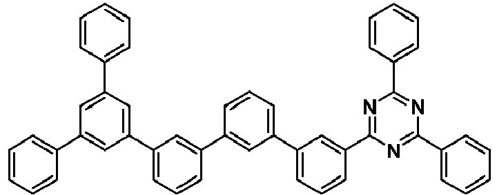
ETM-29 
ETM-30 
ETM-31 
ETM-32 
ETM-33 
ETM-34 
ETM-35 
ETM-36 
ETM-37 
ETM-38 
- Table 5 below shows the dipole moments of representative examples of the first organic matrix compound with a dipole moment ≥ 0 Debye and ≤ 2.5 Debye.
Table 5 Reference Name Structure Dipole moment / Debye ADN 9,10-di(naphthalen-2-yl)anthracene 
0.01 ETM-2 Tri(naphthalen-1-yl)borane 
0.14 ETM-8 bis(2-methylnaphthalen-1-yl)(3-(phenanthren-9-yl)phenyl)borane 
0.18 ETM-15 7-(3-(pyren-1-yl)phenyl)dibenzo[c,h]acri dine 
1.80 ETM-17 7-(3-(pyridin-4-yl)phenyl)dibenzo[c,h]acri dine 
2.26 ETM-18 14-(3-(pyren-1-yl)phenyl)dibenzo [a,j] acrid ine 
2.50 ETM-21 7-(3-(pyren-1-yl)phenyl)benzo[c]acridine 
2.13 ETM-29 2-(3-(phenanthren-9-yl)-5-(pyridin-2-yl)phenyl)-4,6-diphenyl-1,3,5-triazine 
1.76 ETM-28 2,4-diphenyl-6-(5"'-phenyl-[1,1':3',1":3",1'":3'",1""-quinquephenyl]-3-yl)-1,3,5-triazine 
0.23 ETM-26 2-([1,1'-biphenyl]-3-yl)-4-(3'-(4,6-diphenyl-1,3,5-triazin-2-yl)-[1,1'-biphenyl]-3-yl)-6-phenyl-1,3,5-triazine 
0.13 ETM-27 2-(3'-(4,6-diphenyl-1,3,5-triazin-2-yl)-[1,1'-biphenyl]-3-yl)-4-phenylbenzo[4,5]thieno[3, 2-d]pyrimidine 
2.0 ETM-32 2-phenyl-4-(4',5',6'-triphenyl-[1,1':2',1":3",1"'-quaterphenyl]-3 "'-yl)benzo[4,5]thieno[3,2-d]pyrimidine 
1.6 ETM-33 7,12-diphenylbenzo[k]fluoranth ene (CAS 16391-62-1) 
0.13 ETM-34 3,9-di(naphthalen-2-yl)perylene (CAS 959611-30-4) 
0.12 - In another aspect, the electron transport layer may comprise a polar first organic matrix compound. Preferably, the first organic matrix compound has a dipole moment of about > 2.5 Debye and < 10 Debye, preferably > 3 and < 5 Debye, even more preferred > 2.5 and less than 4 Debye.
- If an organic matrix compounds has a dipole moment of > 2.5 and < 10 Debye, the organic matrix compound may be described by one of the following symmetry groups: C1, Cn, Cnv, or Cs.
- When an organic matrix compound has a dipole moment of > 2.5 and < 10 Debye, the organic matrix compound may comprise benzofurane, dibenzofurane, dinaphthofurane, pyridine, acridine, phenyltriazole, benzimidazole, phenanthroline, oxadiazole, benzooxazole, oxazole, quinazoline, benzoquinazoline, pyrido[3,2-h]quinazoline, pyrimido[4,5-f]quinazoline, quinoline, benzoquinoline, pyrrolo[2,1-a]isoquinolin, benzofuro[2,3-d]pyridazine, thienopyrimidine, phosphine oxide, phosphole or mixtures thereof.
- It is further preferred that the first organic matrix compound comprises a phosphine oxide compound substituted with C6-C40 aryl, C5-C40 heteroaryl and/or C1-C12 alkyl groups, preferably (3-(dibenzo[c,h]acridin-7-yl)phenyl)diphenylphosphine oxide, 3-phenyl-3H-benzo[b]dinaphtho[2,1-d:1',2'- f]phosphepine-3-oxide, phenyldi(pyren-1-yl)phosphine oxide, bis(4-(anthracen-9-yl)phenyl)(phenyl)phosphine oxide, (3-(9,10-di(naphthalen-2-yl)anthracen-2-yl)phenyl)diphenylphosphine oxide, phenyldi(pyren-1-yl)phosphine oxide, diphenyl(5-(pyren-1-yl)pyridin-2-yl)phosphine oxide, diphenyl(4'-(pyren-1-yl)-[1,1'-biphenyl]-3-yl)phosphine oxide, diphenyl(4'-(pyren-1-yl)-[1,1'-biphenyl]-3-yl)phosphine oxide, (3'-(dibenzo[c,h]acridin-7-yl)-[1,1'-biphenyl]-4-yl)diphenylphosphine oxide and/or phenyl bis(3-(pyren-1-yl)phenyl)phosphine oxide.
- Diarylphosphine oxide compounds which may be used as first organic matrix compound are disclosed in
EP 2395571 A1 ,WO2013079217 A1 ,EP 13187905 EP13199361 JP2002063989 A1 EP15195877.4 - It is further preferred that the first organic matrix compound comprises a benzimidazole compound substituted with C6-C40 aryl, C5-C40 heteroaryl and/or C1-C12 alkyl groups, preferably 2-(4-(9,10-di(naphthalen-2-yl)anthracene-2-yl)phenyl)-1-phenyl-1H-benzo[d]imidazole, 1-(4-(10-([1,1'-biphenyl]-4-yl)anthracen-9-yl)phenyl)-2-ethyl-1H-benzo[d]imidazole, and/or 1,3,5-tris(1-phenyl-1H-benzimidazol-2-yl)benzene.
- Benzimidazole compounds that can be used as first organic matrix materials are disclosed in
US 6878469 andWO2010134352 . - In a preferred embodiment, the first organic matrix compound comprises a quinoline compound. Suitable quinoline compounds are disclosed in
US 20090108746 andUS 20090166670 . - In a preferred embodiment, the first organic matrix matrix compound comprises a benzoquinoline compound. Suitable benzoquinoline compounds are disclosed in
JP 2004281390 US 20120280613 . - In a preferred embodiment, the first organic matrix compound comprises a pyrimidine compound. Suitable pyrimidine compounds are disclosed in
JP2004031004 - In a preferred embodiment, the first organic matrix compound comprises an oxazole compound. Preferred oxazole compounds are disclosed in
JP2003007467 WO2014163173 . - In a preferred embodiment, the first organic matrix compound comprises an oxadiazole compound. Preferred oxadiazole compounds are disclosed in
US2015280160 . - In a preferred embodiment, the first organic matrix compound comprises an benzooxazole compound. Preferred benzooxazole compounds are disclosed in Shirota and Kageyama, Chem. Rev. 2007, 107, 953-1010.
- In a preferred embodiment, the first organic matrix compound comprises a triazole compound. Suitable triazole compounds are disclosed in
US2015280160 . - In a preferred embodiment, the first organic matrix compound comprises a pyrimido[4,5-f]quinazoline compound. Suitable pyrimido[4,5-f]quinazoline compounds are disclosed in
EP2504871 . - In a preferred embodiment, the first organic matrix compound may be selected from the group consisting of a compound represented by
Formula 2, and a compound represented byFormula 3 below:

- In
Formulae - For example, R1 to R6 may be each independently selected from the group consisting of a hydrogen atom, a halogen atom, a hydroxy group, a cyano group, a methyl group, an ethyl group, a propyl group, a butyl group, a methoxy group, an ethoxy group, a propoxy group, a butoxy group, a phenyl group, a naphthyl group, an anthryl group, a pyridinyl group, and a pyrazinyl group.
- In particular, in
Formula 2 and/or 3, R1 to R4 may each be a hydrogen atom, R5 may be selected from the group consisting of a halogen atom, a hydroxy group, a cyano group, a methyl group, an ethyl group, a propyl group, a butyl group, a methoxy group, an ethoxy group, a propoxy group, a butoxy group, a phenyl group, a naphthyl group, an anthryl group, a pyridinyl group, and a pyrazinyl group. In addition, inFormula 3, R1 to R6 may each be a hydrogen atom. - For example, in
Formula 2 and/or 3, Q1 to Q9 are each independently a hydrogen atom, a phenyl group, a naphthyl group, an anthryl group, a pyridinyl group, and a pyrazinyl group. In particular, inFormulae 2 and/or 3, Q1, Q3-Q6, Q8 and Q9 are hydrogen atoms, and Q2 and Q7 may be each independently selected from the group consisting of a phenyl group, a naphthyl group, an anthryl group, a pyridinyl group, and a pyrazinyl group. - For example, L1, in
Formula 2 and/or 3, may be selected from the group consisting of a phenylene group, a naphthylene group, an anthrylene group, a pyridinylene group, and a pyrazinylene group. In particular, L1 may be a phenylene group or a pyridinylene group. For example, "a" maybe 1, 2, or, 3. - The first organic matrix compound may be further selected from
Compound 5, 6, or 7 below:
- Preferably, the first organic matrix compound comprises a phenanthroline compound substituted with C6-C40 aryl, C5-C40 heteroaryl and/or C1-C12 alkyl groups, preferably 2,4,7,9-tetraphenyl-1,10-phenanthroline, 4,7-diphenyl-2,9-di-p-tolyl-1,10-phenanthroline, 2,9-di(biphenyl-4-yl)-4,7-diphenyl-1,10-phenanthroline and/or 3,8-bis(6-phenyl-2-pyridinyl)- 1, 10-phenanthroline.
- Phenanthroline compounds that can be used as first organic matrix materials are disclosed in
EP 1786050 A1 andCN102372708 . - Other suitable first organic matrix compounds that can be used are quinazoline compounds substituted with aryl or heteroaryl groups, preferably 9-phenyl-9'-(4-phenyl-2-quinazolinyl)- 3,3'-bi-9H-carbazole. It is further preferred that the first organic matrix compound comprises a quinazoline compound substituted with C6-C40 aryl, C5-C40 heteroaryl and/or C1-C12 alkyl groups, preferably 9-phenyl-9'-(4-phenyl-2-quinazolinyl)- 3,3'-bi-9H-carbazole. Quinazoline compounds that can be used as first organic matrix materials are disclosed in
KR2012102374 - It is further preferred that the first organic matrix compound comprises a benzo[h]quinazoline compound substituted with C6-C40 aryl, C5-C40 heteroaryl and/or C1-C12 alkyl groups, preferably 4-(2-naphthalenyl)-2-[4-(3-quinolinyl)phenyl]- benzo[h]quinazoline. Benzo[h]quinazoline compounds that can be used as first organic matrix materials are disclosed in
KR2014076522 - It is also preferred that the first organic matrix compound comprises a pyrido[3,2-h]quinazoline compound substituted with C6-C40 aryl, C5-C40 heteroaryl and/or C1-C12 alkyl groups, preferably 4-(naphthalen-1-yl)-2,7,9-triphenylpyrido[3,2-h]quinazoline. Pyrido[3,2-h]quinazoline compounds that can be used as first organic matrix materials are disclosed in
EP1970371 . - In a further preferred embodiment, the first organic matrix compound is selected from acridine compounds. Suitable acridine compounds are disclosed in
CN104650032 . - Extraordinary preferred first organic matrix compounds are that of the following structures of Table 6.
Table 6 First organic matrix compounds with a dipole moment >2.5 Debye and ≤10 Debye which may be suitable used Compound Structure ETM-35 
ETM-36 
ETM-37 
ETM-38 
ETM-39 
ETM-40 
ETM-41 
ETM-42 
ETM-43 
ETM-44 
ETM-45 
ETM-46 
ETM-47 
ETM-48 
ETM-49 
ETM-50 
ETM-51 
ETM-52 
- Table 7 below shows the dipole moments of representative examples of the first organic matrix compound with a dipole moment of >2.5 Debye and ≤10 Debye.
Table 7 Compound Name Structure Dipole moment/Debye ETM-53 1,2-diphenyl-1H-benzo[d]imidazole 
3.75 ETM-54 Triphenylphosphine oxide 
3.97 ETM-55 4,7-diphenyl-1,10-phenanthroline 
3.65 ETM-56 9-phenyl-9'-(quinazolin-2-yl)-9H,9'H-3,3'-bicarbazole 
3.2 / 1.65*) ETM-51 4-(2-naphthalenyl)-2-[4-(3-quinolinyl)phenyl] -benzo[ h ] quinazoline 
3 ETM-52 4-(naphthalen-1-yl)-2,7,9-triphenylpyrido[3,2-h]quinazoline 
3.81 *) Two conformers with a difference of 1 kJ/mol difference in total energy. Therefore, both conformers are present at room temperature. - According to another aspect, the electron transport layer can be in direct contact with the electron injection layer according to the invention comprises a first organic matrix compound. If more than one electron transport layer is present, the electron injection layer is contacting sandwiched between the first electron transport layer comprising the first organic matrix compound and the first cathode electrode layer. The second electron transport layer, if present, is contacting sandwiched between the emission layer and the first electron transport layer.
- According to a preferred embodiment, the first electron transport layer comprises a first organic matrix compound with a dipole moment of ≥ 0 Debye and ≤ 2.5 Debye, and the second electron transport layer comprises a second organic matrix compound with a dipole moment of > 2.5 Debye and ≤10 Debye.
- Preferably, the organic phosphine compound in the electron injection layer and the second organic matrix compound in the second electron transport layer are selected the same.
- In a particularly preferred embodiment, the organic phosphine compound in the electron injection layer and the second organic matrix compound in the second electron transport layer are selected the same, and the first electron transport layer comprises a first organic matrix compound with a dipole moment of ≥ 0 Debye and ≤ 2.5 Debye, Thereby, low operating voltage and/or high external quantum efficiency EQE and/or high TACT time are achieved.
- According to various embodiments of the OLED of the present invention the thicknesses of the electron transport layer may be in the range of about ≥ 0.5 nm to about ≤ 95 nm, preferably of about ≥ 3 nm to about ≤ 80 nm, further preferred of about ≥ 5 nm to about ≤ 60 nm, also preferred of about ≥ 6 nm to about ≤ 40 nm, in addition preferred about ≥ 8 nm to about ≤ 20 nm and more preferred of about ≥ 10 nm to about ≤ 18 nm.
- According to various embodiments of the OLED of the present invention the thicknesses of the electron transport layer stack can be in the range of about ≥ 25 nm to about ≤ 100 nm, preferably of about ≥ 30 nm to about ≤ 80 nm, further preferred of about ≥ 35 nm to about ≤ 60 nm, and more preferred of about ≥ 36 nm to about ≤ 40 nm.
- The ETL may be formed optional on an EML or on the HBL if the HBL is formed.
- The ETL may have a stacked structure, preferably of two ETL-layers, so that injection and transport of electrons may be balanced and holes may be efficiently blocked. In a conventional OLED, since the amounts of electrons and holes vary with time, after driving is initiated, the number of excitons generated in an emission area may be reduced. As a result, a carrier balance may not be maintained, so as to reduce the lifetime of the OLED.
- However, in the ETL, the first layer and the second layer may have similar or identical energy levels, so that the carrier balance may be uniformly maintained, while controlling the electron-transfer rate.
- The organic light emitting device may comprise further electron transport layers, preferably a third and optional fourth electron transport layer, wherein the third and optional fourth electron transport layer is arranged between the charge generation layer and the cathode. Preferably, the first electron transport layer and third electron transport layer are selected the same, and the second and fourth electron transport layer are selected the same.
- The ETL may be formed on the EML by vacuum deposition, spin coating, slot-die coating, printing, casting, or the like. When the ETL is formed by vacuum deposition or spin coating, the deposition and coating conditions may be similar to those for formation of the HIL. However, the deposition and coating conditions may vary, according to a compound that is used to form the ETL.
- The substrate may be any substrate that is commonly used in manufacturing of organic light-emitting diodes. If light is emitted through the substrate, the substrate may be a transparent material, for example a glass substrate or a transparent plastic substrate, having excellent mechanical strength, thermal stability, transparency, surface smoothness, ease of handling, and waterproofness. If light is emitted through the top surface, the substrate may be a transparent or non-transparent material, for example a glass substrate, a plastic substrate, a metal substrate or a silicon substrate.
- The anode electrode may be formed by depositing or sputtering a compound that is used to form the anode electrode. The compound used to form the anode electrode may be a high work-function compound, so as to facilitate hole injection. The anode material may also be selected from a low work function material (i.e. Aluminum).The anode electrode may be a transparent or reflective electrode. Transparent conductive compounds, such as indium tin oxide (ITO), indium zinc oxide (IZO), tin-dioxide (SnO2), and zinc oxide (ZnO), may be used to form the
anode electrode 120. Theanode electrode 120 may also be formed using magnesium (Mg), aluminum (Al), aluminum-lithium (Al-Li), calcium (Ca), magnesium-indium (Mg-In), magnesium-silver (Mg-Ag), silver (Ag), gold (Au), or the like. - The anode electrode may be formed from a high conductivity metal, for example copper (Cu) or silver (Ag).
- A hole injection layer (HIL), comprising a first and/or second hole injection layer, that can be suitable used for the OLED of the present invention are described in
US2002158242 AA EP1596445A1 andEP1988587A1 . - The first HIL may be formed on the anode electrode by vacuum deposition, spin coating, printing, casting, slot-die coating, Langmuir-Blodgett (LB) deposition, or the like.
- The second HIL may be formed on the n-type charge generation layer by vacuum deposition, spin coating, slot-die coating, printing, casting, Langmuir-Blodgett (LB) deposition, or the like.
- When the HIL is formed using vacuum deposition, the deposition conditions may vary according to the compound that is used to form the HIL, and the desired structure and thermal properties of the HIL. In general, however, conditions for vacuum deposition may include a deposition temperature of 100° C to 500° C, a pressure of 10-8 to 10-3 torr (1 torr equals 133.322 Pa), and a deposition rate of 0.1 to 10 nm/sec..
- For example, the coating conditions may include a coating speed of about 2000 rpm to about 5000 rpm, and a thermal treatment temperature of about 80° C to about 200° C. Thermal treatment removes a solvent after the coating is performed.
- A hole transport layer (HTL), comprising a first and/or second hole transport layer, that can be suitable used for the OLED of the present invention are described in Shirota and Kageyama, Chem. Rev. 2007, 107, 953-1010.
- The first hole transport layer (HTL) may be formed on the HIL by vacuum deposition, spin coating, slot-die coating, printing, casting, Langmuir-Blodgett (LB) deposition, or the like.
- The second hole transport layer (HTL) may be formed on the second hole injection layerby vacuum deposition, spin coating, slot-die coating, printing, casting, Langmuir-Blodgett (LB) deposition, or the like.
- When the HTL is formed by vacuum deposition or spin coating, the conditions for deposition and coating may be similar to those for the formation of the HIL. However, the conditions for the vacuum or solution deposition may vary, according to the compound that is used to form the HTL.
- The function of the electron blocking layer (EBL) 150 is to prevent electrons from being transferred from the emission layer to the hole transport layer and thereby confine electrons to the emission layer. Thereby, efficiency, operating voltage and/or lifetime are improved. Typically, the electron blocking layer comprises a triarylamine compound. The triarylamine compound may have a LUMO level closer to vacuum level than the LUMO level of the hole transport layer. The electron blocking layer may have a HOMO level that is further away from vacuum level compared to the HOMO level of the hole transport layer. The thickness of the electron blocking layer is selected between 2 and 20 nm.
- The electron blocking layer may comprise a compound of Formula Z below

- In Formula Z,
CY1 and CY2 are the same as or different from each other, and each independently represent a benzene cycle or a naphthalene cycle,
Ar1 to Ar3 are the same as or different from each other, and each independently selected from the group consisting of hydrogen; a substituted or unsubstituted aryl group having 6 to 30 carbon atoms; and a substituted or unsubstituted heteroaryl group having 5 to 30 carbon atoms,
Ar4 is selected from the group consisting of a substituted or unsubstituted phenyl group, a substituted or unsubstituted biphenyl group, a substituted or unsubstituted terphenyl group, a substituted or unsubstituted triphenylene group, and a substituted or unsubstituted heteroaryl group having 5 to 30 carbon atoms,
L is a substituted or unsubstituted arylene group having 6 to 30 carbon atoms. - If the electron blocking layer has a high triplet level, it may also be described as triplet control layer.
- The function of the triplet control layer is to reduce quenching of triplets if a phosphorescent green or blue emission layer is used. Thereby, higher efficiency of light emission from a phosphorescent emission layer can be achieved. The triplet control layer is selected from triarylamine compounds with a triplet level above the triplet level of the phosphorescent emitter in the adjacent emission layer. Suitable triplet control layer, in particular the triarylamine compounds, are described in
EP 2 722 908 A1 - The EML may be formed on the HTL by vacuum deposition, spin coating, slot-die coating, printing, casting, LB, or the like. When the EML is formed using vacuum deposition or spin coating, the conditions for deposition and coating may be similar to those for the formation of the HIL.
- The first emission layer may be formed on the first hole transport layer.
- The second emission layer may be formed on the second hole transport layer.
- However, the conditions for deposition and coating may vary, according to the compound that is used to form the EML.
- The emission layer (EML) may be formed of a combination of a host and a dopant. Example of the host are Alq3, 4,4'-N,N'- dicarbazole-biphenyl (CBP), poly(n-vinylcarbazole) (PVK), 9,10-di(naphthalene-2-yl)anthracenee (ADN), 4,4',4"-Tris(carbazol-9-yl)-triphenylamine (TCTA), 1,3,5-tris(N-phenylbenzimidazole-2-yl)benzene (TPBI), 3-tert-butyl-9,10-di-2-naphthylanthracenee (TBADN), distyrylarylene (DSA), Bis(2-(2-hydroxyphenyl)-benzothiazolate)zinc (Zn(BTZ) 2), E3 below, AND,
Compound 12 below, and Compound 13 below.


- The dopant may be a phosphorescent or fluorescent emitter. Phosphorescent emitters and emitters which emit light via a thermally activated delayed fluorescence (TADF) mechanism are preferred due to their higher efficiency. The emitter may be a small molecule or a polymer. Examples of a red dopant are PtOEP, Ir(piq)3, and Btp 2lr(acac), but are not limited thereto. These compounds are phosphorescent emitters, however, fluorescent red dopants could also be used.

- Examples of a phosphorescent green dopant are Ir(ppy)3 (ppy = phenylpyridine), Ir(ppy)2(acac), Ir(mpyp)3 are shown below.
Compound 14 is an example of a fluorescent green emitter and the structure is shown below.

- Examples of a phosphorescent blue dopant are F2Irpic, (F2ppy)2Ir(tmd) and Ir(dfppz) 3, ter-fluorene, the structures are shown below. 4.4'-bis(4-diphenyl amiostyryl)biphenyl (DPAVBi), 2,5,8,11-tetra-tert-butyl perylene (TBPe), and Compound 15 below are examples of fluorescent blue dopants.


- The amount of the dopant may be in the range of about 0.01 to about 50 parts by weight, based on 100 parts by weight of the host. Alternatively, the emission layer may consist of a light-emitting polymer. The EML may have a thickness of about 10 nm to about 100 nm, for example, about 20 nm to about 60 nm. When the thickness of the EML is within this range, the EML may have excellent light emission, without a substantial increase in driving voltage.
- In a preferred embodiment, the electron injection layer according to the invention is contacting sandwiched between the emission layer comprising a light-emitting polymer and the first cathode electrode layer.
- When the EML comprises a phosphorescent dopant, a hole blocking layer (HBL) may be formed on the EML, by using vacuum deposition, spin coating, slot-die coating, printing, casting, LB deposition, or the like, in order to prevent the diffusion of triplet excitons or holes into the ETL.
- Hole blocking layer that can be suitable used for the OLED of the present invention are described in
US2015207093A andUS2015060794A , and fully incorporated by reference. - When the HBL is formed using vacuum deposition or spin coating, the conditions for deposition and coating may be similar to those for the formation of the HIL. However, the conditions for deposition and coating may vary, according to the compound that is used to form the HBL. Any compound that is commonly used to form a HBL may be used. Examples of compounds for forming the HBL include an oxadiazole derivative, a triazole derivative, a triazine derivative, an acridine derivative, and a phenanthroline derivative.
- If the hole blocking layer has a high triplet level, it may also be described as triplet control layer. The function of the triplet control layer is to reduce quenching of triplets if a phosphorescent green or blue emission layer is used. Thereby, higher efficiency of light emission from a phosphorescent emission layer can be achieved. The triplet control layer is selected from a heteroaryl compound with a triplet level above the triplet level of the phosphorescent emitter in the adjacent emission layer.
- The first hole blocking layer may be formed on the first emission layer.
- The second hole blocking layer may be formed on the second emission layer.
- The HBL may have a thickness of about 5 nm to about 100 nm, for example, about 10 nm to about 30 nm. When the thickness of the HBL is within this range, the HBL may have excellent hole-blocking properties, without a substantial increase in driving voltage.
- Charge generation layers (CGL) that can be suitable used for the OLED of the present invention are described in
US 2012098012 A . - The charge generation layer is generally composed of a double layer. The charge generation layer can be a pn junction charge generation layer joining n-type charge generation layer and p-type charge generation layer. The pn junction charge generation layer generates charges or separates them into holes and electrons; and injects the charges into the individual light emission layer. In other words, the n-type charge generation layer provides electrons for the first light emission layer adjacent to the anode electrode while the p-type charge generation layer provides holes to the second light emission layer adjacent to the cathode electrode, by which luminous efficiency of an organic light emitting device incorporating multiple light emission layers can be further improved and at the same time, driving voltage can be lowered.
- The p-type charge generation layer can be composed of metal or organic material doped with p-type dopant. Here, the metal can be one or an alloy consisting of two or more selected from a group consisting of Al, Cu, Fe, Pb, Zn, Au, Pt, W, In, Mo, Ni, and Ti. Also, p-type dopant and host used for organic material doped with the p-type can employ conventional materials. For example, the p-type dopant can be one selected from a group consisting of tetrafluore-7,7,8,8-tetracyanoquinodimethane (F4-TCNQ), derivative of tetracyanoquinodimethane, radialene derivative, iodine, FeCl3, FeF3, and SbC15. Also, the host can be one selected from a group consisting of N,N'-di(naphthalen-1-yl)-N,N-diphenyl-benzidine (NPB), N,N'-diphenyl-N,N'-bis(3-methylphenyl)-1,1-biphenyl-4,4'-diamine (TPD) and N,N',N'-tetranaphthyl-benzidine (TNB).
- The n-type charge generation layer can be composed of metal or organic material doped with n-type. The metal can be one selected from a group consisting of Li, Na, K, Rb, Cs, Mg, Ca, Sr, Ba, La, Ce, Sm, Eu, Tb, Dy, and Yb. Also, n-type dopant and host used for organic material doped with the n-type can employ conventional materials. For example, the n-type dopant can be alkali metal, alkali metal compound, alkali earth metal, or alkali earth metal compound. More specifically, the n-type dopant can be one selected from a group consisting of Cs, K, Rb, Mg, Na, Ca, Sr, Eu and Yb. The host material can be one selected from a group consisting of tris(8-hydroxyquinoline)aluminum, triazine, hydroxyquinoline derivative, benzazole derivative, and silole derivative.
- In another preferred embodiment, the n-type charge generation layer is arranged adjacent to the electron transport layer. The n-type charge generation layer according to one embodiment may include compounds of the following
Chemical Formula 16.
- each of A1 to A6 may be hydrogen, a halogen atom, nitrile (-CN), nitro (-NO2), sulfonyl (-SO2R), sulfoxide (-SOR), sulfonamide (-SO2NR), sulfonate (-SO3R), trifluoromethyl (-CF3), ester (-COOR), amide (-CONHR or - CONRR'), substituted or unsubstituted straight-chain or branched-chain C1-C12 alkoxy, substituted or unsubstituted straight-chain or branched-chain C1-C12 alkyl, substituted or unsubstituted straight-chain or branched chain C2-C12 alkenyl, a substituted or unsubstituted aromatic or non-aromatic heteroring, substituted or unsubstituted aryl, substituted or unsubstituted mono- or diarylamine, substituted or unsubstituted aralkylamine, or the like.
- Herein, each of the above R and R' may be substituted or unsubstituted C1-C60 alkyl, substituted or unsubstituted aryl, or a substituted or unsubstituted 5- to 7-membered heteroring, or the like.
- Particularly preferred is an n-type charge generation layer comprising a compound of Formula (17)

- The p-type charge generation layer is arranged on top of the n-type charge generation layer. As the materials for the p-type charge generation layer, aryl amine-based compounds may be used. One embodiment of the aryl amine-based compounds includes compounds of the following Chemical Formula 18:

- Ar1, Ar2 and Ar3 are each independently hydrogen or a hydrocarbon group. Herein, at least one of Ar1, Ar2 and Ar3 may include aromatic hydrocarbon substituents, and each substituent may be the same, or they may be composed of different substituents. When Ar1, Ar2 and Ar3 are not aromatic hydrocarbons, they may be hydrogen; a straight-chain, branched-chain or cyclic aliphatic hydrocarbon; or a heterocyclic group including N, O, S or Se.
- In another aspect of the present invention, the organic light emitting diode (100) further comprises an n-type CGL (185), a p-type CGL (135) and an ETL stack (160), wherein the ETL stack (160) comprises a first electron transport layer (160a) comprising a first organic matrix compound selected from organic phosphine compound and a second electron transport layer (160b) comprising a second organic matrix compound. Preferably, the organic phosphine compound is selected from the group of organic phosphine oxide, organic thioxophosphine compound and/or an organic selenoxophosphine compound, and the second organic matrix compound is selected from an organic compound with a dipole moment of about ≥ 0 Debye and about ≤ 2.5 Debye. In a particularly preferred embodiment, the electron injection layer (180) and the first electron transport layer (160) comprise the same organic phosphine compound. In a preferred embodiment, the n-type CGL comprises or consists of the first zero-valent metal.
- According to another aspect of the present invention, there is provided an organic light-emitting diode (OLED) comprising: a substrate, an anode electrode a hole injection layer, a hole transport layer, optional an electron blocking layer, an emission layer, optional a hole blocking layer, optional an electron transport layer, an electron injection layer, and a first cathode electrode layer, wherein the layers are arranged in that order.
- According to another aspect of the present invention, there is provided an organic light-emitting diode (OLED) comprising: a substrate, an anode electrode a first hole injection layer, a first hole transport layer, optional first electron blocking layer, a first emission layer, optional a first hole blocking layer, optional a first electron transport layer, an n-type charge generation layer, an p-type charge generation layer, a second hole transport layer, optional second electron blocking layer a second emission layer, optional a second hole blocking layer, optional a second electron transport layer, an electron injection layer, a first cathode electrode layer, and a second cathode electrode layer, wherein the layers are arranged in that order.
- According to various embodiments of the OLED of the present invention, the OLED may not comprises an electron transport layer.
- According to various embodiments of the OLED of the present invention, the OLED may not comprises an electron blocking layer.
- According to various embodiments of the OLED of the present invention, the OLED may not comprises a hole blocking layer.
- According to various embodiments of the OLED of the present invention, the OLED may not comprises a charge generation layer.
- According to various embodiments of the OLED of the present invention, the OLED may not comprises a second emission layer.
- According to various embodiments of the present invention, the method may further include forming on a substrate an anode electrode a hole injection layer, a hole transport layer, optional an electron blocking layer, an emission layer, optional a hole blocking layer, optional an electron transport layer, an electron injection layer, and a first cathode electrode layer, wherein the layers are arranged in that order; or the layers can be deposited the other way around, starting with the first cathode electrode layer, and more preferred the first electron injection layer is be deposited before the first cathode electrode layer is deposited.
- Particularly low operating voltage and/or high external quantum efficiency EQE may be achieved when the electron injection layer is deposited before the first cathode electrode layer.
- According to various embodiments of the present invention, the method may further include forming on a substrate an anode electrode a first hole injection layer, a first hole transport layer, optional first electron blocking layer, a first emission layer, optional a first hole blocking layer, optional a first electron transport layer, an n-type charge generation layer, an p-type charge generation layer, a second hole transport layer, optional second electron blocking layer, a second emission layer, optional a second hole blocking layer, optional a second electron transport layer, an electron injection layer, a first cathode electrode layer, and a second cathode electrode layer, wherein the layers are arranged in that order; or the layers are deposited the other way around, starting with the second cathode electrode layer; and more preferred the second injection layer is be deposited before the first cathode electrode layer is deposited.
- However, according to one aspect the layers are deposited the other way around, starting with the cathode electrode, and sandwiched between the cathode electrode and the anode electrode.
- For example, starting with the first cathode electrode layer, electron injection layer, optional electron transport layer, optional hole blocking layer, emission layer, optional electron blocking layer, hole transport layer, hole injection layer, anode electrode, exactly in this order.
- The anode electrode and/or the cathode electrode can be deposited on a substrate. Preferably the anode is deposited on a substrate.
- According to another aspect of the present invention, there is provided a method of manufacturing an organic light-emitting diode (OLED), the method using:
- at least one deposition source, preferably two deposition sources and more preferred at least three deposition sources; and/or
- deposition via vacuum thermal evaporation; and/or
- deposition via solution processing, preferably the processing is selected from spin-coating, printing, casting and/or slot-die coating.
- Another aspect is directed to an electronic device comprising at least one organic light-emitting diode (OLED). A device comprising organic light-emitting diodes (OLED) is for example a display or a lighting panel.
- Additional aspects and/or advantages of the invention will be set forth in part in the description which follows and, in part, will be obvious from the description, or may be learned by practice of the invention.
- These and/or other aspects and advantages of the present invention will become apparent and more readily appreciated from the following description of the exemplary embodiments, taken in conjunction with the accompanying drawings, of which:
-
FIG. 1 is a schematic sectional view of an organic light-emitting diode (OLED), according to an exemplary embodiment of the present invention; -
FIG. 2 is a schematic sectional view of an OLED, according to an exemplary embodiment of the present invention. -
FIG. 3 . is a schematic sectional view of an OLED, according to another exemplary embodiment of the present invention. -
FIG. 4 is a schematic sectional view of a tandem OLED comprising a charge generation layer, according to an exemplary embodiment of the present invention. -
FIG. 5 is a schematic sectional view of a tandem OLED comprising a charge generation layer and an ETL stack, according to an exemplary embodiment of the present invention -
FIG. 6 is a graph showing the operating voltage of an OLED according to invention plotted against the layer thickness of the electron injection layer according to invention. - Reference will now be made in detail to the exemplary embodiments of the present invention, examples of which are illustrated in the accompanying drawings, wherein like reference numerals refer to the like elements throughout. The exemplary embodiments are described below, in order to explain the aspects of the present invention, by referring to the figures.
- Herein, when a first element is referred to as being formed or disposed "on" a second element, the first element can be disposed directly on the second element, or one or more other elements may be disposed there between. When a first element is referred to as being formed or disposed "directly on" a second element, no other elements are disposed there between.
-
FIG. 1 is a schematic sectional view of an organic light-emitting diode (OLED) 100, according to an exemplary embodiment of the present invention. TheOLED 100 includes asubstrate 110, ananode electrode 120, a hole injection layer (HIL) 130, a hole transport layer (HTL) 140, an emission layer (EML) 150, an electron transport layer (ETL) 160. Onto the electron transport layer (ETL) 160 an electron injection layer (EIL) 180 is disposed. The electron injection layer (EIL) 180 comprising or consisting of an organic phosphine compound selected from the group of organic phosphine oxide compound or an organic thioxophosphine compound or an organic selenoxophosphine compound, wherein the electron injection layer (EIL) 180 is formed directly on theETL 160. The firstcathode electrode layer 191 is disposed directly onto the electron injection layer (EIL) 180. - Instead of a single
electron transport layer 160, optional an electron transport layer stack (ETL) can be used. -
Fig. 2 is a schematic sectional view of anOLED 100, according to another exemplary embodiment of the present invention.Fig. 2 differs fromFig. 1 in that theOLED 100 ofFig. 2 comprises an electron blocking layer (EBL) 145 and an electron transport layer stack (ETL stack) 160. - Referring to
Fig. 2 theOLED 100 includes asubstrate 110, ananode electrode 120, a hole injection layer (HIL) 130, a hole transport layer (HTL) 140, an electron blocking layer (EBL) 145, an emission layer (EML) 150, an electron transport layer stack (ETL) 160 and an electron injection layer (EIL 180). TheETL stack 160 comprises a first electron transport layer (ETL1) 160a and a second electron transport layer (ETL2) 160b. The secondelectron transport layer 160b is disposed directly on theemission layer 150. The firstelectron transport layer 160a is disposed directly on the second electron transport layer. The electron injection layer (EIL) 180 comprising or consisting of an organic phosphine compound selected from the group of an organic phosphine oxide compound or an organic thioxophosphine compound or an organic selenoxophosphine compound, is disposed directly on the firstelectron transport layer 160a. The firstcathode electrode layer 191 is disposed directly onto the electron injection layer (EIL) 180. -
Fig. 3 is a schematic sectional view of anOLED 100, according to another exemplary embodiment of the present invention.Fig. 3 differs fromFig. 1 in that theOLED 100 ofFig. 2 comprises an electron blocking layer (EBL) 145, a hole blocking layer (HBL) 155 and a secondcathode electrode layer 192. - Referring to
Fig. 3 theOLED 100 includes asubstrate 110, ananode electrode 120, a hole injection layer (HIL) 130, a hole transport layer (HTL) 140, an electron blocking layer (EBL) 145, an 181 (EML) 150, a hole blocking layer (HBL) 155, an electron transport layer (ETL) 160 and an electron injection layer (EIL) 180. The electron injection layer (EIL) 180 comprising or consisting of an organic phosphine compound selected from the group of an organic phosphine oxide compound or an organic thioxophosphine compound or an organic selenoxophosphine compound, wherein the electron injection layer (EIL) 180 is disposed directly on theETL 160. The firstcathode electrode layer 191 is disposed directly onto the electron injection layer (EIL) 180. The secondcathode electrode layer 192 is disposed directly onto the firstcathode electrode layer 191. The first and second cathode electrode layer together form thecathode electrode 190. - In the description above the method of manufacture an
OLED 100 of the present invention is started with asubstrate 110 onto which ananode electrode 120 is formed, on theanode electrode 120, anhole injection layer 130,hole transport layer 140, optional anelectron blocking layer 145, anemission layer 150, optional ahole blocking layer 155, optional at least oneelectron transport layer 160, anelectron injection layer 180, a firstcathode electrode layer 191 and an optional secondcathode electrode layer 192 are formed, in that order or the other way around. -
Fig. 4 is a schematic sectional view of atandem OLED 100, according to another exemplary embodiment of the present invention.Fig. 4 differs fromFig. 2 in that theOLED 100 ofFig. 4 further comprises a charge generation layer and a second emission layer. - Referring to
Fig. 4 the OLED 200 includes asubstrate 110, ananode electrode 120, a first hole injection layer (HIL) 130, a first hole transport layer (HTL) 140, a first electron blocking layer (EBL) 145, a first emission layer (EML) 150, a first hole blocking layer (HBL) 155, a first electron transport layer (ETL) 160, an n-type charge generation layer (n-type CGL) 185, a p-type charge generation layer (p-type GCL) 135, a second hole transport layer (HTL) 141, a second electron blocking layer (EBL) 146, a second emission layer (EML) 151, a second hole blocking layer (EBL) 156, a second electron transport layer (ETL) 161, an electron injection layer (EIL) 180, a firstcathode electrode layer 191 and a secondcathode electrode layer 192. Theelectron injection layer 180 comprising or consisting of an organic phosphine compound selected from the group of organic phosphine oxide compound or an organic thioxophosphine compound or an organic selenoxophosphine compound is disposed directly onto the secondelectron transport layer 161 and the firstcathode electrode layer 191 is disposed directly onto theelectron injection layer 180. - In the description above the method of manufacture an
OLED 100 of the present invention is started with asubstrate 110 onto which ananode electrode 120 is formed, on theanode electrode 120, a firsthole injection layer 130, firsthole transport layer 140, optional a firstelectron blocking layer 145, afirst emission layer 150, optional a firsthole blocking layer 155, optional anETL stack 160, comprising a firstelectron transport layer 160a and a secondelectron transport layer 160b, an n-type CGL 185, a p-type CGL 135, a secondhole transport layer 141, optional a secondelectron blocking layer 146, asecond emission layer 151, an optional secondhole blocking layer 156, an optional at least one secondelectron transport layer 161, anelectron injection layer 180, a firstcathode electrode layer 191 and an optional secondcathode electrode layer 192 are formed, in that order or the other way around. -
Fig. 5 is a schematic sectional view of atandem OLED 100, according to another exemplary embodiment of the present invention.Fig. 5 differs fromFig. 4 in that theOLED 100 ofFig. 5 further comprises anETL stack 160. - Referring to
Fig. 5 the OLED 200 includes asubstrate 110, ananode electrode 120, a first hole injection layer (HIL) 130, a first hole transport layer (HTL) 140, a first electron blocking layer (EBL) 145, a first emission layer (EML) 150, a first hole blocking layer (HBL) 155, an ETL stack (ETL) 160, an n-type charge generation layer (n-type CGL) 185, a p-type charge generation layer (p-type GCL) 135, a second hole transport layer (HTL) 141, a second electron blocking layer (EBL) 146, a second emission layer (EML) 151, a second hole blocking layer (EBL) 156, a third electron transport layer (ETL) 161, an electron injection layer (EIL) 180, a firstcathode electrode layer 191 and a secondcathode electrode layer 192. TheETL stack 160 comprises a first electron transport layer (ETL1) 160a and a second electron transport layer (ETL2) 160b. The secondelectron transport layer 160b is disposed directly on thefirst emission layer 150. The firstelectron transport layer 160a is disposed directly on the secondelectron transport layer 160b. Theelectron injection layer 180 comprising or consisting of an organic phosphine compound selected from the group of organic phosphine oxide compound or an organic thioxophosphine compound or an organic selenoxophosphine compound is disposed directly onto the secondelectron transport layer 161 and the firstcathode electrode layer 191 is disposed directly onto theelectron injection layer 180. - While not shown in
Fig. 1, Fig. 2 ,Fig. 3 ,Fig. 4 andFig. 5 , a sealing layer may further be formed on thecathode electrodes 190, in order to seal theOLEDs 100 and 200. In addition, various other modifications may be applied thereto. -
Fig. 6 shows the effect of the thickness of the electron injection layer (EIL) according to invention on the operating voltage of a fluorescent blue OLED. Organic phosphine compound (Va) is used as electron injection layer with a thickness ranging from 1 to 10 nm. 2 nm Yb is used as first cathode electrode layer. 100 nm Al is used as second cathode electrode layer. The electron injection layer is contacting sandwiched between an electron transport layer and the first cathode electrode layer. The electron transport layer comprises non-polar anthracene compound ETM-1 and the thickness is 34 nm. The emission layer comprises 97 wt.-% of ABH113 (Sun Fine Chemicals) as a host and 3 wt.-% of NUBD370 (Sun Fine Chemicals) as a fluorescent blue dopant. The lowest operating voltage is achieved for an EIL thickness of more than 1 nm and less than 6 nm. A thickness range of ≥ 1 nm and ≤ 5 nm is particularly preferred. The lowest operating voltage is observed for an EIL thickness of 3 to 4 nm. - For bottom emission devices - Examples 1 to 10 and comparative examples 1 to 2, a 15Ω /
cm 2 glass substrate (available from Corning Co.) with 100 nm Ag was cut to a size of 50 mm x 50 mm x 0.7 mm, ultrasonically cleaned with isopropyl alcohol for 5 minutes and then with pure water for 5 minutes, and cleaned again with UV ozone for 30 minutes, to prepare a first electrode. - Then, 92 wt.-% of Biphenyl-4-yl(9,9-diphenyl-9H-fluoren-2-yl)-[4-(9-phenyl-9H-carbazol-3-yl)phenyl]-amine and 8 wt.-% of 2,2',2"-(cyclopropane-1,2,3-triylidene)tris(2-(p-cyanotetrafluorophenyl)acetonitrile) was vacuum deposited on the ITO electrode, to form a HIL having a thickness of 10 nm. Then Biphenyl-4-yl(9,9-diphenyl-9H-fluoren-2-yl)-[4-(9-phenyl-9H-carbazol-3-yl)phenyl]-amine was vacuum deposited on the HIL, to form a HTL having a thickness of 120 nm. 97 wt.-% of ABH 113 (Sun Fine Chemicals) as a host and 3 wt.-% of NUBD370 (Sun Fine Chemicals) as a dopant were deposited on the HTL, to form a blue-emitting EML with a thickness of 20 nm.
- Then, the electron transport layer is formed by deposing a first organic matrix compound according to examples 1 to 10 and comparative example 1 and 2 by deposing the compound from a first deposition source directly on the EML. Further, the thickness d (in nm) of the ETL can be taken from Table 8.
- Then, the electron injection layer is formed by deposing an organic phosphine compound according to example 1 to 10 and comparative examples 1 and 2 directly on the electron transport layer. The composition and thickness of the electron injection layer can be taken from Table 8.
- For comparative example 2, a 0.4 nm thick layer of LiF is deposited on the electron injection layer, thereby forming a second electron injection layer.
- The first cathode electrode layer is evaporated at ultra-high vacuum of 10-7 bar. Therefore, a thermal single co-evaporation of one or several metals is performed with a rate of 0, 1 to 10 nm/s (0.01 to 1 Å/s) in order to generate a homogeneous cathode electrode with a thickness of 5 to 1000 nm. Then, the optional second cathode electrode layer is deposed directly on to the first cathode electrode layer under the same conditions. The composition and thickness of the first and second cathode electrode layer can be taken from Table 8.
- The OLED stack is protected from ambient conditions by encapsulation of the device with a glass slide. Thereby, a cavity is formed, which includes a getter material for further protection.
- For bottom emission devices, a 15Ω /
cm 2 glass substrate (available from Corning Co.) with 100 nm Ag was cut to a size of 50 mm x 50 mm x 0.7 mm, ultrasonically cleaned with isopropyl alcohol for 5 minutes and then with pure water for 5 minutes, and cleaned again with UV ozone for 30 minutes, to prepare a first electrode. - Then, PEDOT:PSS (Clevios P VP AI 4083) is spin-coated directly on top of the first electrode to form a 55 nm thick HIL. The HIL is baked on hotplate at 150 °C for 5 min. Then, a light-emitting polymer, for example MEH-PPV, is spin-coated directly on top of the HIL to form a 40 nm thick EML. The EML is baked on a hotplate at 80 °C for 10 min. The device is transferred to an evaporation chamber and the following layers are deposited in high vacuum.
- Organic phosphine compound (Vr) is deposed directly on top of the EML to form an EIL with a thickness of 4 nm. A first cathode electrode layer is formed by depositing a 2 nm thick layer of ytterbium directly on top of the EIL. A second cathode electrode layer is formed by deposing a 100 nm thick layer of aluminium directly on top of the first cathode electrode layer.
- For top emission devices - Examples 11 to 15, the anode electrode was formed from 100 nm silver on glass which is prepared by the same methods as described above.
- Then, 92 wt.-% of biphenyl-4-yl(9,9-diphenyl-9H-fluoren-2-yl)-[4-(9-phenyl-9H-carbazol-3-yl)phenyl]-amine (CAS 1242056-42-3) and 8 wt.-% of 2,2',2"-(cyclopropane-1,2,3-triylidene)tris(2-(p-cyanotetrafluorophenyl)acetonitrile) is vacuum deposited on the ITO elec-trode, to form a HIL having a thickness of 10 nm. Then biphenyl-4-yl(9,9-diphenyl-9H-fluoren-2-yl)-[4-(9-phenyl-9H-carbazol-3-yl)phenyl]-amine (CAS 1242056-42-3) is vacuum deposited on the HIL, to form a HTL having a thickness of 125 nm. Then N,N-bis(4-(dibenzo[b,d]furan-4-yl)phenyl)-[1,1':4',1"-terphenyl]-4-amine is deposed directly on top of the HTL to form an EBL with a thickness of 5 nm.
- 97 wt.-% of 2-(10-phenyl-9-anthracenyl)-benzo[b]naphtho[2,3-d]furan as a host and 3 wt.-% of NUBD370 (Sun Fine Chemicals) as a dopant are deposited on the EBL, to form a blue-emitting EML with a thickness of 20 nm.
- Then the electron transport layer is formed by deposing a first organic matrix compound according to examples 10 to 15 by deposing the compound from a first deposition source directly on the EML. Further, the thickness d (in nm) of the ETL can be taken from Table 9.
- Then, the electron injection layer according to the invention is formed by deposing an organic phosphine compound according to examples 11 to 15 directly on the electron transport layer. The composition and thickness of the electron injection layer can be taken from Table 9.
- The first cathode electrode layer is evaporated at ultra-high vacuum of 10-7 bar. Therefore, a thermal single co-evaporation of one or several metals is performed with a rate of 0, 1 to 10 nm/s (0.01 to 1 Å/s) in order to generate a homogeneous cathode electrode with a thickness of 5 to 1000 nm. Then, the optional second cathode electrode layer is deposed directly on to top of the first cathode electrode layer under the same conditions. The composition and thickness of the first and second cathode electrode layer can be taken from Table 9.
- 60 nm biphenyl-4-yl(9,9-diphenyl-9H-fluoren-2-yl)-[4-(9-phenyl-9H-carbazol-3-yl)phenyl]-amine (CAS 1242056-42-3) is deposed directly on top of the second cathode electrode layer.
- The OLED stack is protected from ambient conditions by encapsulation of the device with a glass slide. Thereby, a cavity is formed, which includes a getter material for further protection.
- To assess the performance of the inventive examples compared to the prior art, the current efficiency is measured under ambient conditions (20°C). Current voltage measurements are performed using a Keithley 2400 sourcemeter, and recorded in V. At 10 mA/cm2 for bottom emission and 10 mA/cm2 for top emission devices, a calibrated spectrometer CAS140 from Instrument Systems is used for measurement of CIE coordinates and brightness in Candela. Lifetime LT of bottom emission device is measured at ambient conditions (20°C) and 10 mA/cm2, using a Keithley 2400 sourcemeter, and recorded in hours. Lifetime LT of top emission device is measured at ambient conditions (20°C) and 8 mA/cm2. The brightness of the device is measured using a calibrated photo diode. The lifetime LT is defined as the time till the brightness of the device is reduced to 97 % of its initial value.
- In bottom emission devices, the emission is predominately Lambertian and quantified in percent external quantum efficiency (EQE). To determine the efficiency EQE in % the light output of the device is measured using a calibrated photodiode at 10 mA/cm2.
- In top emission devices, the emission is forward directed, non-Lambertian and also highly dependent on the mirco-cavity. Therefore, the efficiency EQE will be higher compared to bottom emission devices. To determine the efficiency EQE in % the light output of the device is measured using a calibrated photodiode at 10 mA/cm2.
- The beneficial effect of the electron injection layer according to the invention on the performance of bottom emission devices can be seen in Table 8.
- An electron transport layer comprising an anthracene compound as first organic matrix compound is used in Example 1 to 10 and in comparative examples 1 and 2. The anthracene compounds may have a dipole moment of ≥ 0 Debye and ≤ 2.5 Debye, see Table 5.
- In comparative example 1, the electron injection layer comprising organic phosphine oxide compound (Vr) is in direct contact with the aluminium cathode electrode. The operating voltage is very at 4.7 V.
- In comparative example 2, the electron injection layer comprising organic phosphine oxide compound (Vr) is in direct contact with a thin layer of LiF. The LiF layer is contacting sandwiched between the electron injection layer and the aluminium cathode electrode. The operating voltage is 3.2 V and thereby significantly lower than in comparative example 1. However, this improvement in operating voltage is achieved by using toxic and thermally unstable LiF.
- In example 1, the electron injection layer comprising organic phosphine oxide compound (Vr) is in direct contact with a first cathode electrode layer of 0.4 nm layer of lithium and a second cathode electrode layer of 100 nm aluminium. The operating voltage is 3.3 V and therefore comparable to comparative example 2. However, this very low operating voltage is achieved by using lithium instead of LiF. Lithiuim is thermally stable and, additionally, it is not a toxic compound and therefore can be easily handled in manufacturing processes. Additionally, the operating voltage is significantly lower than in comparative example 1, where high workfuntion metal aluminium is used. Lithium has a workfunction of 2.95 eV while aluminium has a workfunction of 4.3 eV. Therefore, the workfunction of lithium is significantly lower than the workfunction of aluminium and it is therefore easier to inject electrons from a lithium layer into the electron injection layer comprising an phosphine compound.
- In example 2, a first cathode electrode layer of 2 nm ytterbium is used in place of lithium. The operating voltage is unchanged. The same operating voltage is obtained in example 3, where barium is used to form the first cathode electrode layer. Ytterbium and barium have a workfunction which is lower than the workfunction of aluminium.
- In example 4 to 10, various electron injection layers comprising an organic phosphine compound of formula (Ia) are tested. In all examples the first cathode electrode layer is formed from 2 nm ytterbium and the second cathode electrode layer is formed from 100 nm aluminium.
- In example 4 to 6, the electron injection layer comprises an organic phosphine compound of formula (II). The operating voltage is 3.3 and 3.4 V.
- In example 7 to 10, the electron injection layer comprises an organic phosphine compound of formula (III). The operating voltage is between 3.2 and 3.4 V.
- In summary, a wide range of organic phosphine compounds can be used in the electron injection layer according to the invention.
Table 8 Bottom emission device comprising an emission layer, electron transport layer (ETL), electron injection layer comprising an organic phosphine compound and a cathode electrode comprising a first cathode electrode layer and optionally a second cathode electrode layer ETL d (ETL) / nm EIL1 d (EIL1) /nm EIL2 d (EIL1) /nm Cathode electrode layer 1 d (cathode electrode layer 1)/ nm Cathode electrode layer 2 d (cathode electrode layer 2) / nm U at 10 mA/cm2/ V Comparative example 1 ADN 36 Compound (Vr) 4 -- -- Al 100 -- -- 4.7 Comparative example 2 ADN 36 Compound (Vr) 4 LiF 0.4 Al 100 -- -- 3.2 Example 1 ETM-1 34 Compound (Vr) 4 -- -- Li 0.4 Al 100 3.3 Example 2 ETM-1 34 Compound (Vr) 4 -- -- Yb 2 Al 100 3.3 Example 3 ETM-1 34 Compound (Vr) 4 -- -- Ba 2 Al 100 3.2 Example 4 ETM-1 34 Compound (Va) 4 -- -- Yb 2 Al 100 3.35 Example 5 ETM-1 34 Compound (Vb) 4 -- -- Yb 2 Al 100 3.3 Example 6 ETM-1 34 Compound (Vd) 4 -- -- Yb 2 Al 100 3.4 Example 7 ETM-1 34 Compound (Vf) 4 -- -- Yb 2 Al 100 3.3 Example 8 ETM-1 34 Compound (Vj) 4 -- -- Yb 2 Al 100 3.2 Example 9 ETM-1 34 Compound (Vq) 4 -- -- Yb 2 Al 100 3.4 Example 10 ETM-1 34 Compound (V1) 4 -- -- Yb 2 Al 100 3.3 - The beneficial effect of the electron injection layer according to the invention on the performance of top emission devices can be seen in Table 9.
- The electron injection layer comprising organic phosphine compound (Vr) is in direct contact with a first cathode electrode layer which consists of 2 nm ytterbium. In example 11 and 12, the second cathode electrode layer consists of 11 nm Ag. In example 13 to 15, the second cathode electrode layer consists of 13 nm MgAg alloy (15:85 vol.-%).
- An electron transport layer is used in examples 11 to 15. The electron transport layer comprises a first organic matrix compound with a dipole moment of ≥ 0 Debye and ≤ 2.5 Debye, see Table 9. In examples 11 and 13 to 15, triazine compound ETM-28 is used. In example 12, dibenzo[c,h]acridine compound ETM-15 is used.
- In all examples, the operating voltage is very low at 3.2 to 3.3 V, the external quantum efficiency is very high at 15.5 to 16.5 % EQE and the lifetime is high at 44 to 60 hours see Table 9.
Table 9 Top emission device comprising an emission layer, electron transport layer (ETL), electron injection layer comprising an organic phosphine compound and a cathode electrode comprising a first cathode electrode layer and a second cathode electrode layer ETL d (ETL) / nm EIL d (EIL) /nm Cathode electrode layer 1 d (cathode electrode layer 1)/ / nm Cathode electrode layer 2 d (cathode electrode layer 2) / nm U at 10 mA/cm2 / V EQE at 10 mA/cm2 /% LT at 8 mA/cm2 /h Example 11 ETM-28 29 Compound (Vr) 4 Yb 2 Ag 11 3.3 16.5 44 Example 12 ETM-15 29 Compound (Vr) 4 Yb 2 Ag 11 3.2 15.6 46 Example 13 ETM-28 29 Compound (Vd) 4 Yb 2 Mg:Ag (15:85 vol.-%) 13 3.2 15.5 60 Example 14 ETM-28 29 Compound (Vq) 4 Yb 2 Mg:Ag (15:85 vol.-%) 13 3.2 15.5 60 Example 15 ETM-28 29 Compound (Vr) 4 Yb 2 Mg:Ag (15:85 vol.-%) 13 3.3 16 50 - From the foregoing detailed description and examples, it will be evident that modifications and variations can be made to the compositions and methods of the invention without departing from the spirit and scope of the invention. Therefore, it is intended that all modifications made to the invention without departing from the spirit and scope of the invention come within the scope of the appended claims.

the first cathode electrode layer comprises a first zero-valent metal selected from the group comprising alkali metal, alkaline earth metal, rare earth metal and/or a

the first cathode electrode layer comprises a first zero-valent metal selected from the group comprising alkali metal, alkaline earth metal, rare earth metal and/or a


Claims (19)
- Organic light emitting diode (100) comprising at least one emission layer (150), an electron injection layer (180) and at least one cathode electrode (190), wherein:- the electron injection layer (180) comprises an organic phosphine compound, wherein the electron injection layer (180) is free of a metal, metal salt, metal complex and metal organic compound;- the cathode electrode (190) comprises at least a first cathode electrode layer (191), wherein- the first cathode electrode layer (191) comprises a first zero-valent metal selected from the group comprising alkali metal, alkaline earth metal, rare earth metal and/or a group 3 transition metal; and- the electron injection layer (180) is arranged in direct contact to the first cathode electrode layer (191).
- The organic light emitting diode (100) according to claim 1, wherein the organic phosphine compound of the electron injection layer (180) is a compound having the Formula Ia:
 X is selected from O, S, Se;R1 and R2 are independently selected from C1 to C12 alkyl, substituted or unsubstituted C6 to C20 aryl or substituted or unsubstituted C5 to C20 heteroaryl; or R1 and R2 are bridged with an alkene-di-yl group forming with the P atom a substituted or unsubstituted five, six or seven membered ring; andA1 is phenyl or selected from Formula (II):
 R3 is selected from C1 to C8 alkane-di-yl, substituted or unsubstituted C6 to C20 arylene, or substituted or unsubstituted C5 to C20 heteroarylene; orA1 is selected from Formula (III)
 n is selected from 0 or 1;m is selected from 1 or 2;o is selected from 1 or 2;and m is 1 if o is 2;Ar1 is selected from substituted or unsubstituted C6 to C20 arylene and substituted or unsubstituted C5 to C20 heteroarylene;Ar2 is selected from substituted or unsubstituted C18 to C40 arylene and substituted or unsubstituted C10 to C40 heteroarylene;R4 is selected from H, C1 to C12 alkyl, substituted or unsubstituted C6 to C20 aryl and substituted or unsubstituted C5 to C20 heteroaryl; whereinthe cathode electrode (190) comprises at least a first cathode electrode layer (191), wherein
the first cathode electrode layer (191) comprises a first zero-valent metal selected from the group comprising alkali metal, alkaline earth metal, rare earth metal and/or a group 3 transition metal; and
the electron injection layer (180) is arranged in direct contact to the first cathode electrode layer (191). - The organic light emitting diode (100) according to claim 1 or 2, wherein the first cathode electrode layer (191) is free of a metal halide and/or free of a metal organic complex.
- The organic light emitting diode (100) according to any one of claims 1 to 3, wherein the first cathode electrode layer (191) further comprises a second zero-valent metal, wherein the second zero-valent metal is selected from a main group metal or a transition metal, wherein the second zero-valent metal is selected different from the first zero-valent metal; preferably the second zero-valent metal is selected from the group comprising Li, Na, K, Cs, Mg, Ca, Sr, Ba, Sc, Y, Ti, V, Cr, Mn, Mn, Fe, Fe, Co, Co, Ni, Cu, Cu, Zn, Ag, Au, Au, Al, Ga, In, Sn, Sn, Te, Bi or Pb; and more preferred the second zero-valent metal is selected from the group comprising Ag, Au, Zn, Te, Yb, Ga, Bi, Ba, Ca, Al; and most preferred the second zero-valent metal is selected from the group comprising Ag, Zn, Te, Yb, Ga, and/or Bi.
- The organic light emitting diode (100) according to any one of claims 1 to 4, wherein the cathode electrode (190) further comprises a second cathode electrode layer (192), wherein the second cathode electrode layer (192) comprises at least a third metal, in form of a zero-valent metal, alloy and/or as oxide, wherein the third metal is selected from a main group metal, transition metal and/or rare earth metal, preferably the third metal is selected from zero-valent Ag, Al, Cu and Au, MgAg alloy, indium tin oxide, indium zinc oxide, ytterbium oxide, indium gallium zinc oxide and more preferred the third metal is selected from Ag and Al, and MgAg alloy; and most preferred the third metal is selected from zero-valent Ag and Al.
- The organic light emitting diode (100) according to any one of claims 1 to 5, further comprising at least one electron transport layer (160) comprising at least one matrix compound, wherein the electron injection layer (180) is contacting sandwiched between the first cathode electrode layer (191) and the electron transport layer (160), wherein the electron transport layer (160) comprises preferably a first organic matrix compound with a dipole moment of about ≥ 0 Debye and about ≤ 2.5 Debye.
- The organic light emitting diode (100) according to any one of claims 1 to 6, wherein- Ar1 is selected from substituted C6 to C20 arylene, and/or substituted C5 to C20 heteroarylene, wherein the C6 to C20 arylene, and/or C5 to C20 heteroarylene is substituted with at least one C1 to C12 alkyl and/or at least one C1 to C12 heteroalkyl group;
Ar2 is selected from substituted C18 to C40 arylene and/or substituted C10 to C40 heteroarylene, wherein the C18 to C40 arylene and/or C10 to C40 heteroarylene is substituted with at least one C1 to C12 alkyl and/or at least one C1 to C12 heteroalkyl group; and- preferably Ar1 = substituted C6 to C20 arylene and/or substituted C5 to C20 heteroarylene, wherein the C6 to C20 arylene and/or C5 to C20 heteroarylene is substituted with at least one C1 to C6 alkyl and/or C1 to C6 heteroalkyl group;
Ar2 = substituted C18 to C40 arylene and/or substituted C10 to C40 heteroarylene, wherein the C18 to C40 arylene and/or C10 to C40 heteroarylene is substituted with at least one C1 to C6 alkyl and/or C1 to C6 heteroalkyl group; and- more preferred Ar1 = substituted C6 to C20 arylene and/or substituted C5 to C20 heteroarylene, wherein the C6 to C20 arylene and/or C5 to C20 heteroarylene is substituted with at least one C1 to C4 alkyl and/or C1 to C4 heteroalkyl group;
Ar2 = substituted C18 to C40 arylene and/or substituted C10 to C40 heteroarylene, wherein the C18 to C40 arylene and/or C10 to C40 heteroarylene is substituted with at least one C1 to C4 alkyl and/or C1 to C4 heteroalkyl group. - The organic light emitting diode (100) according to any one of claims 1 to 7, whereinR1 and R2 are independently selected from substituted C6 to C20 aryl, or substituted C5 to C20 heteroaryl, wherein the C6 to C20 aryl, and/or C5 to C20 heteroaryl is substituted with at least one C1 to C12 alkyl and/or at least one C1 to C12 heteroalkyl group, and preferably R1 and R2 is selected the same; and/orR3 is independently selected from substituted C6 to C20 arylene, or substituted C5 to C20 heteroarylene, wherein the C6 to C20 arylene, and/or C5 to C20 heteroarylene is substituted with at least one C1 to C12 alkyl and/or at least one C1 to C12 heteroalkyl group; and/orR4 is independently selected from substituted C6 to C20 aryl, or substituted C5 to C20 heteroaryl, wherein the C6 to C20 aryl, and/or C5 to C20 heteroaryl is substituted with at least one C1 to C12 alkyl and/or at least one C1 to C12 heteroalkyl group.
- The organic light emitting diode (100) according to any one of claims 1 to 8, wherein for- o = 2 the organic phosphine compound of the electron injection layer (180) is a compound having the Formula Ib:
 - o = 1 the organic phosphine compound of the electron injection layer (180) is a compound having the Formula Ic, Id, Ie or If:

- The organic light emitting diode (100) according to any one of claims 1 to 9, whereinR1 and R2 is independently selected from C1 to C4 alkyl, unsubstituted or substituted C6 to C10 aryl, or unsubstituted or substituted C5 to C10 heteroaryl, wherein the C6 to C10 aryl, and/or C5 to C10 heteroaryl is substituted with at least one C1 to C12 alkyl and/or at least one C1 to C12 heteroalkyl group, and preferably R1 and R2 is selected the same; preferably R1 and R2 is independently selected from methyl, phenyl, naphthyl, phenanthryl, pyrenyl or pyridyl; further preferred R1 and R2 are independently selected from methyl, phenyl and pyridyl; and more preferred R1 and R2 is selected the same; and/orX is O or S, and preferably O; and/orR3 is selected from C1 to C6 alkane-di-yl, unsubstituted or substituted C6 to C10 arylene or unsubstituted or substituted C5 to C10 heteroarylene, and preferably selected from C1 to C4 alkane-di-yl; and/orR4 is selected from H, phenyl, biphenyl, terphenyl, fluorenyl, naphthyl, anthranyl, phenanthryl, pyrenyl, carbazoyl, dibenzofuranyl, dinapthofuranyl, preferably H, phenyl, biphenyl or naphthyl, and more preferred H; and/orn is 0, 1 or 2, preferably n is 1 or 2, further preferred for n = 2 than Ar1 is phenyl, and more preferred for n = 1, R1 and R2 are phenyl and R4 is H;m is 1 or 2 and n is 0 or 1, or m is 2 and n is 2; and/orAr1 is selected from phenylene, biphenylene, terphenylene, naphthylene, fluorenylene, pyridylene, quinolinylene, and pyrimidinylene; and/orAr2 is selected from fluorenylene, anthranylene, pyrenylene, phenanthrylene, carbazoylene, benzo[c]acridinylene, dibenzo[c,h]acridinylene, dibenzo[a,j]acridinylene.
- The organic light emitting diode (100) according to any one of claims 1 to 10, wherein R1, R2, R3, R4, Ar1 and/or Ar2 are unsubstituted.
- The organic light emitting diode (100) according to any one of claims 1 to 11, wherein Ar2 is selected from a compound according to Formula IVa to IVh:


- The organic light emitting diode (100) according to any one of claims 1 to 12, wherein the compound of Formula (I) is selected from a compound according to:- Formula Va to Ve:

 - Formula Vf to Vq:


 - Formula Vr to Vt:

- The organic light emitting diode (100) according to any one of claims 1 to 13, wherein the first matrix compound is an organic matrix compound selected from the group comprising benzo[k]fluoranthene, pyrene, anthracene, fluorene, spiro(bifluorene), phenanthrene, perylene, triptycene, spiro[fluorene-9,9'-xanthene], coronene, triphenylene, xanthene, benzofurane, dibenzofurane, dinaphthofurane, acridine, benzo[c]acridine, dibenzo[c,h]acridine, dibenzo[a,j]acridine, triazine, pyridine, pyrimidine, carbazole, phenyltriazole, benzimidazole, phenanthroline, oxadiazole, benzooxazole, oxazole, quinazoline, benzo[h]quinazoline, pyrido[3,2-h]quinazoline, pyrimido[4,5-f]quinazoline, quinoline, benzoquinoline, pyrrolo[2,1-a]isoquinolin, benzofuro[2,3-d]pyridazine, thienopyrimidine, dithienothiophene, benzothienopyrimidine, benzothienopyrimidine, phosphine oxide, phosphole, triaryl borane, 2-(benzo[d]oxazol-2-yl)phenoxy metal complex, 2-(benzo[d]thiazol-2-yl)phenoxy metal complex or mixtures thereof.
- The organic light emitting diode (100) according to any one of claims 1 to 14, wherein the OLED comprises a substrate (110), an anode electrode (120), a hole injection layer (130), a hole transport layer (140), optional an electron blocking layer (145), an emission layer (150), optional a hole blocking layer (155), optional an electron transport layer (160), an electron injection layer (180), a first cathode electrode layer (191), and an optional second cathode electrode layer (192) wherein the layers are arranged in that order.
- The organic light emitting diode (100) according to any one of claims 1 to 15, wherein the OLED comprises a substrate (110), an anode electrode (120), a first hole injection layer (130), a first hole transport layer (140), optional first electron blocking layer (145), a first emission layer (150), optional a first hole blocking layer (155), optional a first electron transport layer (160), an n-type charge generation layer (185), a p-type charge generation layer (135), a second hole transport layer (141), optional second electron blocking layer (146), a second emission layer (151), optional a second hole blocking layer (156), optional a second electron transport layer (161), an electron injection layer (180), a first cathode electrode layer (191), and an optional second cathode electrode layer (192), wherein the layers are arranged in that order.
- A method of manufacturing an organic light emitting diode (100), according to any of claims 1 to 16, wherein- on the substrate (110) an anode electrode is deposited and on the anode electrode the other layers of hole injection layer (130), hole transport layer (140), optional an electron blocking layer (145), emission layer (150), optional hole blocking layer (155), optional electron transport layer (160), electron injection layer (180), and first cathode electrode layer (191), are deposited in that order; or- the layers are deposited the other way around, starting with the first cathode electrode layer (191);- more preferred the first electron injection layer (180) is deposited before the first cathode electrode layer (191) is deposited.
- A method of manufacturing an organic light emitting diode (100), according to any of claims 1 to 16, wherein- on the substrate (110) an anode electrode is deposited and on the anode electrode the other layers of first hole injection layer (130), first hole transport layer (140), optional first electron blocking layer (145), a first emission layer (150), optional first hole blocking layer (155), optional first electron transport layer (160), n-type charge generation layer (185), p-type charge generation layer (135), second hole transport layer (141), optional second electron blocking layer (146), second emission layer (151), optional second hole blocking layer (156), optional second electron transport layer (161), electron injection layer (180), first cathode electrode layer (191), and second cathode electrode layer (192), are deposited in that order; or- the layers are deposited the other way around, starting with the second cathode electrode layer (192);- more preferred the electron injection layer (180) is deposited before the first cathode electrode layer (191) is deposited.
- Electronic device comprising at least one organic light emitting diode (100), according to any of claims 1 to 16.
Priority Applications (6)
| Application Number | Priority Date | Filing Date | Title |
|---|---|---|---|
| EP15201418.9A EP3182478B1 (en) | 2015-12-18 | 2015-12-18 | Electron injection layer for an organic light-emitting diode (oled) |
| CN201680073099.5A CN108463898B (en) | 2015-12-18 | 2016-12-14 | Electron injection layer for Organic Light Emitting Diodes (OLEDs) |
| KR1020187020541A KR20180097653A (en) | 2015-12-18 | 2016-12-14 | An electron injection layer for an organic light emitting diode (OLED) |
| PCT/EP2016/080958 WO2017102822A1 (en) | 2015-12-18 | 2016-12-14 | Electron injection layer for an organic light-emitting diode (oled) |
| JP2018531095A JP7022063B2 (en) | 2015-12-18 | 2016-12-14 | Electron injection layer for organic light emitting diodes (OLEDs) |
| US16/062,974 US20190006589A1 (en) | 2015-12-18 | 2016-12-14 | Electron Injection Layer for an Organic Light-Emitting Diode (OLED) |
Applications Claiming Priority (1)
| Application Number | Priority Date | Filing Date | Title |
|---|---|---|---|
| EP15201418.9A EP3182478B1 (en) | 2015-12-18 | 2015-12-18 | Electron injection layer for an organic light-emitting diode (oled) |
Publications (2)
| Publication Number | Publication Date |
|---|---|
| EP3182478A1 true EP3182478A1 (en) | 2017-06-21 |
| EP3182478B1 EP3182478B1 (en) | 2018-11-28 |
Family
ID=54979490
Family Applications (1)
| Application Number | Title | Priority Date | Filing Date |
|---|---|---|---|
| EP15201418.9A Active EP3182478B1 (en) | 2015-12-18 | 2015-12-18 | Electron injection layer for an organic light-emitting diode (oled) |
Country Status (6)
| Country | Link |
|---|---|
| US (1) | US20190006589A1 (en) |
| EP (1) | EP3182478B1 (en) |
| JP (1) | JP7022063B2 (en) |
| KR (1) | KR20180097653A (en) |
| CN (1) | CN108463898B (en) |
| WO (1) | WO2017102822A1 (en) |
Cited By (8)
| Publication number | Priority date | Publication date | Assignee | Title |
|---|---|---|---|---|
| US20180114920A1 (en) * | 2016-10-24 | 2018-04-26 | Novaled Gmbh | Electron Transport Layer Stack for an Organic Light-Emitting Diode |
| EP3425692A1 (en) * | 2017-07-07 | 2019-01-09 | Novaled GmbH | Organic electroluminescent device comprising an electron injection layer with zero-valent metal |
| CN112567546A (en) * | 2018-07-02 | 2021-03-26 | 诺瓦尔德股份有限公司 | Electronic device, method of manufacturing the same, and display apparatus including the same |
| EP3923364A1 (en) * | 2020-06-12 | 2021-12-15 | Novaled GmbH | Organic light emitting diode and device comprising the same |
| EP3923363A1 (en) * | 2020-06-12 | 2021-12-15 | Novaled GmbH | Organic light emitting diode and device comprising the same |
| WO2021250279A1 (en) * | 2020-06-12 | 2021-12-16 | Novaled Gmbh | Organic light emitting diode and device comprising the same |
| EP4141980A1 (en) * | 2021-08-24 | 2023-03-01 | Novaled GmbH | Organic light emitting diode and a compound for use therein |
| EP4141979A1 (en) * | 2021-08-24 | 2023-03-01 | Novaled GmbH | Organic light emitting diode and a compound for use therein |
Families Citing this family (15)
| Publication number | Priority date | Publication date | Assignee | Title |
|---|---|---|---|---|
| DE102017101077A1 (en) * | 2017-01-20 | 2018-07-26 | Osram Oled Gmbh | Organic electronic component |
| EP3503241B1 (en) | 2017-12-22 | 2022-08-24 | Novaled GmbH | Electronic device and method for preparing the same |
| EP3503242B1 (en) | 2017-12-22 | 2021-08-25 | Novaled GmbH | Semiconducting material, a method for preparing the same and electronic device |
| CN111406060B (en) * | 2018-02-02 | 2023-02-03 | 株式会社Lg化学 | Heterocyclic compound and organic light-emitting element comprising same |
| CN110590847B (en) * | 2018-10-08 | 2022-02-25 | 苏州大学 | Preparation method of 2,2' - (1, 4-phenylene) bis (1-phenylphosphine heteroindole-1-oxide) |
| EP3643720B1 (en) * | 2018-10-23 | 2021-09-29 | Novaled GmbH | Organic compounds, organic semiconductor layer and organic electronic device |
| EP3667755A1 (en) * | 2018-12-14 | 2020-06-17 | Novaled GmbH | Organic light emitting device, a method for manufacturing the same and a composition for use therein |
| CN109897065B (en) * | 2019-04-16 | 2021-06-01 | 武汉华星光电半导体显示技术有限公司 | Thermal activation delayed fluorescent material, preparation method thereof and organic light-emitting diode device |
| EP3730482A1 (en) * | 2019-04-24 | 2020-10-28 | Novaled GmbH | Compound and an organic semiconducting layer, an organic electronic device and a display or lighting device comprising the same |
| CN111848617B (en) * | 2019-04-25 | 2022-02-22 | 上海钥熠电子科技有限公司 | Organic electroluminescent material and application thereof |
| WO2021038475A1 (en) * | 2019-08-27 | 2021-03-04 | Oti Lumionics Inc. | Light transmissive electrode for light emitting devices |
| CN110563763A (en) * | 2019-09-29 | 2019-12-13 | 上海天马有机发光显示技术有限公司 | compound and application thereof |
| KR102331370B1 (en) | 2020-01-08 | 2021-11-26 | 삼성디스플레이 주식회사 | Light emitting device, method for manufacturing the same, and apparatus including the same |
| EP4060756A1 (en) | 2021-03-19 | 2022-09-21 | Idemitsu Kosan Co., Ltd. | An organic electroluminescence device comprising an azine compound and a rare earth metal, rare earth metal compound, and/or rare earth metal complex and an electronic equipment comprising said organic electroluminescence device |
| CN113702789B (en) * | 2021-08-11 | 2022-07-29 | 电子科技大学 | Detection method for high-energy small-radius electron beam of traveling wave tube |
Citations (48)
| Publication number | Priority date | Publication date | Assignee | Title |
|---|---|---|---|---|
| JP2002063989A (en) | 2000-06-08 | 2002-02-28 | Toray Ind Inc | Light emitting element |
| US20020158242A1 (en) | 1999-12-31 | 2002-10-31 | Se-Hwan Son | Electronic device comprising organic compound having p-type semiconducting characteristics |
| JP2003007467A (en) | 2001-06-19 | 2003-01-10 | Honda Motor Co Ltd | Organic electroluminescence element |
| US20030168970A1 (en) | 2000-11-24 | 2003-09-11 | Tsuyoshi Tominaga | Luminescent element material and luminescent element comprising the same |
| JP2004031004A (en) | 2002-06-24 | 2004-01-29 | Konica Minolta Holdings Inc | Organic electroluminescent element and display device |
| JP2004281390A (en) | 2003-02-25 | 2004-10-07 | Toray Ind Inc | Material for light emitting element, and light emitting element using the same |
| US20050025993A1 (en) | 2003-07-25 | 2005-02-03 | Thompson Mark E. | Materials and structures for enhancing the performance of organic light emitting devices |
| JP2005032686A (en) | 2003-07-11 | 2005-02-03 | Fuji Photo Film Co Ltd | Organic electroluminescent element and aromatic condensed ring compound |
| US6878469B2 (en) | 2002-01-18 | 2005-04-12 | Lg Chem, Ltd. | Material for transporting electrons and organic electroluminescent display using the same |
| EP1596445A1 (en) | 2003-12-04 | 2005-11-16 | Novaled GmbH | Process for doping organic semiconductors with derivatives of diiminoquinones |
| WO2006122630A1 (en) * | 2005-05-20 | 2006-11-23 | Merck Patent Gmbh | Compounds for organic electronic devices |
| EP1786050A1 (en) | 2005-11-10 | 2007-05-16 | Novaled AG | Doped organic semiconductor material |
| US20070202354A1 (en) | 2004-04-15 | 2007-08-30 | Idemitsu Kosan Co.,Ltd | Organic Electroluminescent Device |
| EP1970371A1 (en) | 2007-03-16 | 2008-09-17 | Novaled AG | Pyrido(3,2-h)chinazolins and/or 5,6-Dihydro derivatives thereof, method for their manufacture and endowed organic semiconductor material containing them |
| EP1988587A1 (en) | 2007-04-30 | 2008-11-05 | Novaled AG | Oxocarbon, pseudo oxocarbon and radialene compounds and their use |
| US20090108746A1 (en) | 2007-10-30 | 2009-04-30 | Sang-Hoon Park | Anthracene-based compound and organic light emitting device employing the same |
| US20090166670A1 (en) | 2007-10-30 | 2009-07-02 | Sang-Hoon Park | Anthracene-based compound and organic light emitting device employing the same |
| WO2010020352A1 (en) | 2008-08-18 | 2010-02-25 | Merck Patent Gmbh | Compounds having electron transport properties, their preparation and use |
| WO2010134352A1 (en) | 2009-05-22 | 2010-11-25 | 出光興産株式会社 | Organic electroluminescent element |
| EP2312663A1 (en) | 2009-10-19 | 2011-04-20 | Novaled AG | Organic electronic device comprising an organic semiconducting material |
| KR20110085784A (en) | 2010-01-21 | 2011-07-27 | (주)씨에스엘쏠라 | Organic light emitting compound and organic light emitting device comprising the same |
| US20110284832A1 (en) | 2008-12-30 | 2011-11-24 | Kyu-Yeol In | Compound for organic optoelectronic device, organic light emitting diode including the same and display including the organic light emitting diode |
| EP2395571A1 (en) | 2010-06-10 | 2011-12-14 | Novaled AG | Organic electronic device comprising an organic semiconducting material |
| CN102372708A (en) | 2010-08-20 | 2012-03-14 | 清华大学 | Pyridyl phenanthroline compound and application |
| US20120098012A1 (en) | 2010-10-21 | 2012-04-26 | Changoh Kim | Organic light emitting diode device |
| KR20120102374A (en) | 2011-03-08 | 2012-09-18 | 롬엔드하스전자재료코리아유한회사 | Novel compounds for organic electronic material and organic electroluminescence device using the same |
| EP2504871A1 (en) | 2009-11-24 | 2012-10-03 | Novaled AG | Organic electronic device comprising an organic semiconducting material |
| US20120280613A1 (en) | 2010-12-31 | 2012-11-08 | Dong-Min Kang | Compound for an organic optoelectronic device, organic light emitting diode including the same, and display including the organic light emitting diode |
| WO2013079217A1 (en) | 2011-11-30 | 2013-06-06 | Novaled Ag | Display |
| WO2013149958A1 (en) | 2012-04-02 | 2013-10-10 | Novaled Ag | Use of a semiconducting compound in an organic light emitting device |
| US20140077190A1 (en) * | 2012-09-14 | 2014-03-20 | Industry-Academic Cooperation Foundation Gyeongsang National University | Phosphine oxide-based compound and organic light-emitting device including the same |
| EP2722908A1 (en) | 2012-10-17 | 2014-04-23 | Novaled AG | Phosphorescent OLED and hole transporting materials for phosphorescent OLEDs |
| US20140135530A1 (en) * | 2011-06-24 | 2014-05-15 | Kyushu University National University Corporation | Novel compound and organic device employing same |
| KR20140076522A (en) | 2012-12-12 | 2014-06-20 | 에스에프씨 주식회사 | An electro luminescent compound and an electroluminescent device comprising the same |
| WO2014163173A1 (en) | 2013-04-04 | 2014-10-09 | Jnc株式会社 | Electron transport material and organic electroluminescent device using same |
| WO2014171541A1 (en) | 2013-04-18 | 2014-10-23 | 東ソー株式会社 | Heterocyclic compound for organic electroluminescence element and application therefor |
| WO2015008866A1 (en) | 2013-07-19 | 2015-01-22 | 東ソー株式会社 | Triazine compound and organic electroluminescent element containing same |
| US20150060794A1 (en) | 2013-09-04 | 2015-03-05 | Samsung Display Co., Ltd. | Organic light emitting device and manufacturing method thereof |
| WO2015049030A2 (en) | 2013-10-02 | 2015-04-09 | Merck Patent Gmbh | Boron-containing compounds |
| JP2015074649A (en) | 2013-10-11 | 2015-04-20 | 東ソー株式会社 | Triazine compounds having 4-pyridyl groups, and organic electroluminescent elements containing the same |
| CN104650032A (en) | 2015-01-23 | 2015-05-27 | 北京鼎材科技有限公司 | Acridine derivatives, and preparation method and application thereof |
| WO2015083948A1 (en) | 2013-12-03 | 2015-06-11 | 덕산네오룩스 주식회사 | Compound for organic electric element, organic electric element using same, and electronic device thereof |
| JP2015126140A (en) | 2013-12-26 | 2015-07-06 | 東ソー株式会社 | Organic electroluminescent device |
| WO2015105313A1 (en) | 2014-01-10 | 2015-07-16 | 삼성에스디아이 주식회사 | Fused-ring compound and organic light-emitting device comprising same |
| US20150207093A1 (en) | 2014-01-17 | 2015-07-23 | Samsung Display Co., Ltd. | Organic light-emitting device |
| US20150207079A1 (en) | 2014-01-20 | 2015-07-23 | Samsung Display Co., Ltd. | Organic light-emitting devices |
| KR20150088712A (en) | 2014-01-24 | 2015-08-03 | 삼성에스디아이 주식회사 | Organic compound and composition and organic optoelectric device and display device |
| US20150280160A1 (en) | 2014-03-28 | 2015-10-01 | Lg Display Co., Ltd. | Organic Light Emitting Device |
Family Cites Families (10)
| Publication number | Priority date | Publication date | Assignee | Title |
|---|---|---|---|---|
| JP4299028B2 (en) * | 2002-03-11 | 2009-07-22 | Tdk株式会社 | Organic EL device |
| JP2004095221A (en) * | 2002-08-29 | 2004-03-25 | Toray Ind Inc | Light-emitting device |
| US20040140758A1 (en) * | 2003-01-17 | 2004-07-22 | Eastman Kodak Company | Organic light emitting device (OLED) display with improved light emission using a metallic anode |
| US6902833B2 (en) * | 2003-04-01 | 2005-06-07 | University Of Southern California | Materials and structures for enhancing the performance or organic light emitting devices |
| DE102004008304A1 (en) * | 2004-02-20 | 2005-09-08 | Covion Organic Semiconductors Gmbh | Organic electronic devices |
| EP1744598B1 (en) * | 2004-04-20 | 2017-05-31 | Kyushu Electric Power Co., Inc. | Organic electroluminescent element and manufacturing method thereof, organic compound containing phosphorus and manufacturing method thereof |
| EP2128217B1 (en) * | 2007-03-07 | 2016-02-17 | Toray Industries, Inc. | Light-emitting device material and light-emitting device |
| WO2012085982A1 (en) * | 2010-12-24 | 2012-06-28 | パナソニック株式会社 | Organic el element and method for producing same |
| EP2887412B1 (en) * | 2013-12-23 | 2016-07-27 | Novaled GmbH | Semiconducting material |
| KR101537500B1 (en) * | 2014-04-04 | 2015-07-20 | 주식회사 엘지화학 | Organic light emitting diode |
-
2015
- 2015-12-18 EP EP15201418.9A patent/EP3182478B1/en active Active
-
2016
- 2016-12-14 KR KR1020187020541A patent/KR20180097653A/en not_active Application Discontinuation
- 2016-12-14 WO PCT/EP2016/080958 patent/WO2017102822A1/en active Application Filing
- 2016-12-14 US US16/062,974 patent/US20190006589A1/en active Pending
- 2016-12-14 JP JP2018531095A patent/JP7022063B2/en active Active
- 2016-12-14 CN CN201680073099.5A patent/CN108463898B/en active Active
Patent Citations (49)
| Publication number | Priority date | Publication date | Assignee | Title |
|---|---|---|---|---|
| US20020158242A1 (en) | 1999-12-31 | 2002-10-31 | Se-Hwan Son | Electronic device comprising organic compound having p-type semiconducting characteristics |
| JP2002063989A (en) | 2000-06-08 | 2002-02-28 | Toray Ind Inc | Light emitting element |
| US20030168970A1 (en) | 2000-11-24 | 2003-09-11 | Tsuyoshi Tominaga | Luminescent element material and luminescent element comprising the same |
| JP2003007467A (en) | 2001-06-19 | 2003-01-10 | Honda Motor Co Ltd | Organic electroluminescence element |
| US6878469B2 (en) | 2002-01-18 | 2005-04-12 | Lg Chem, Ltd. | Material for transporting electrons and organic electroluminescent display using the same |
| JP2004031004A (en) | 2002-06-24 | 2004-01-29 | Konica Minolta Holdings Inc | Organic electroluminescent element and display device |
| JP2004281390A (en) | 2003-02-25 | 2004-10-07 | Toray Ind Inc | Material for light emitting element, and light emitting element using the same |
| JP2005032686A (en) | 2003-07-11 | 2005-02-03 | Fuji Photo Film Co Ltd | Organic electroluminescent element and aromatic condensed ring compound |
| US20050025993A1 (en) | 2003-07-25 | 2005-02-03 | Thompson Mark E. | Materials and structures for enhancing the performance of organic light emitting devices |
| EP1596445A1 (en) | 2003-12-04 | 2005-11-16 | Novaled GmbH | Process for doping organic semiconductors with derivatives of diiminoquinones |
| US20070202354A1 (en) | 2004-04-15 | 2007-08-30 | Idemitsu Kosan Co.,Ltd | Organic Electroluminescent Device |
| WO2006122630A1 (en) * | 2005-05-20 | 2006-11-23 | Merck Patent Gmbh | Compounds for organic electronic devices |
| EP1786050A1 (en) | 2005-11-10 | 2007-05-16 | Novaled AG | Doped organic semiconductor material |
| EP1970371A1 (en) | 2007-03-16 | 2008-09-17 | Novaled AG | Pyrido(3,2-h)chinazolins and/or 5,6-Dihydro derivatives thereof, method for their manufacture and endowed organic semiconductor material containing them |
| EP1988587A1 (en) | 2007-04-30 | 2008-11-05 | Novaled AG | Oxocarbon, pseudo oxocarbon and radialene compounds and their use |
| US20090108746A1 (en) | 2007-10-30 | 2009-04-30 | Sang-Hoon Park | Anthracene-based compound and organic light emitting device employing the same |
| US20090166670A1 (en) | 2007-10-30 | 2009-07-02 | Sang-Hoon Park | Anthracene-based compound and organic light emitting device employing the same |
| WO2010020352A1 (en) | 2008-08-18 | 2010-02-25 | Merck Patent Gmbh | Compounds having electron transport properties, their preparation and use |
| US20110284832A1 (en) | 2008-12-30 | 2011-11-24 | Kyu-Yeol In | Compound for organic optoelectronic device, organic light emitting diode including the same and display including the organic light emitting diode |
| WO2010134352A1 (en) | 2009-05-22 | 2010-11-25 | 出光興産株式会社 | Organic electroluminescent element |
| EP2312663A1 (en) | 2009-10-19 | 2011-04-20 | Novaled AG | Organic electronic device comprising an organic semiconducting material |
| EP2504871A1 (en) | 2009-11-24 | 2012-10-03 | Novaled AG | Organic electronic device comprising an organic semiconducting material |
| KR20110085784A (en) | 2010-01-21 | 2011-07-27 | (주)씨에스엘쏠라 | Organic light emitting compound and organic light emitting device comprising the same |
| EP2395571A1 (en) | 2010-06-10 | 2011-12-14 | Novaled AG | Organic electronic device comprising an organic semiconducting material |
| CN102372708A (en) | 2010-08-20 | 2012-03-14 | 清华大学 | Pyridyl phenanthroline compound and application |
| US20120098012A1 (en) | 2010-10-21 | 2012-04-26 | Changoh Kim | Organic light emitting diode device |
| US20120280613A1 (en) | 2010-12-31 | 2012-11-08 | Dong-Min Kang | Compound for an organic optoelectronic device, organic light emitting diode including the same, and display including the organic light emitting diode |
| KR20120102374A (en) | 2011-03-08 | 2012-09-18 | 롬엔드하스전자재료코리아유한회사 | Novel compounds for organic electronic material and organic electroluminescence device using the same |
| US20140135530A1 (en) * | 2011-06-24 | 2014-05-15 | Kyushu University National University Corporation | Novel compound and organic device employing same |
| WO2013079217A1 (en) | 2011-11-30 | 2013-06-06 | Novaled Ag | Display |
| WO2013149958A1 (en) | 2012-04-02 | 2013-10-10 | Novaled Ag | Use of a semiconducting compound in an organic light emitting device |
| US20140077190A1 (en) * | 2012-09-14 | 2014-03-20 | Industry-Academic Cooperation Foundation Gyeongsang National University | Phosphine oxide-based compound and organic light-emitting device including the same |
| EP2722908A1 (en) | 2012-10-17 | 2014-04-23 | Novaled AG | Phosphorescent OLED and hole transporting materials for phosphorescent OLEDs |
| KR20140076522A (en) | 2012-12-12 | 2014-06-20 | 에스에프씨 주식회사 | An electro luminescent compound and an electroluminescent device comprising the same |
| WO2014163173A1 (en) | 2013-04-04 | 2014-10-09 | Jnc株式会社 | Electron transport material and organic electroluminescent device using same |
| WO2014171541A1 (en) | 2013-04-18 | 2014-10-23 | 東ソー株式会社 | Heterocyclic compound for organic electroluminescence element and application therefor |
| WO2015008866A1 (en) | 2013-07-19 | 2015-01-22 | 東ソー株式会社 | Triazine compound and organic electroluminescent element containing same |
| US20150060794A1 (en) | 2013-09-04 | 2015-03-05 | Samsung Display Co., Ltd. | Organic light emitting device and manufacturing method thereof |
| WO2015049030A2 (en) | 2013-10-02 | 2015-04-09 | Merck Patent Gmbh | Boron-containing compounds |
| JP2015074649A (en) | 2013-10-11 | 2015-04-20 | 東ソー株式会社 | Triazine compounds having 4-pyridyl groups, and organic electroluminescent elements containing the same |
| WO2015083948A1 (en) | 2013-12-03 | 2015-06-11 | 덕산네오룩스 주식회사 | Compound for organic electric element, organic electric element using same, and electronic device thereof |
| JP2015126140A (en) | 2013-12-26 | 2015-07-06 | 東ソー株式会社 | Organic electroluminescent device |
| WO2015105313A1 (en) | 2014-01-10 | 2015-07-16 | 삼성에스디아이 주식회사 | Fused-ring compound and organic light-emitting device comprising same |
| WO2015105316A1 (en) | 2014-01-10 | 2015-07-16 | 삼성에스디아이 주식회사 | Fused-ring compound and organic light-emitting device comprising same |
| US20150207093A1 (en) | 2014-01-17 | 2015-07-23 | Samsung Display Co., Ltd. | Organic light-emitting device |
| US20150207079A1 (en) | 2014-01-20 | 2015-07-23 | Samsung Display Co., Ltd. | Organic light-emitting devices |
| KR20150088712A (en) | 2014-01-24 | 2015-08-03 | 삼성에스디아이 주식회사 | Organic compound and composition and organic optoelectric device and display device |
| US20150280160A1 (en) | 2014-03-28 | 2015-10-01 | Lg Display Co., Ltd. | Organic Light Emitting Device |
| CN104650032A (en) | 2015-01-23 | 2015-05-27 | 北京鼎材科技有限公司 | Acridine derivatives, and preparation method and application thereof |
Non-Patent Citations (2)
| Title |
|---|
| ADACHI, C.; TOKITO, S.; TSUTSUI, T.; SAITO, S., JAPANESE JOURNAL OF APPLIED PHYSICS, vol. 27, no. 2, 1988, pages L269 - L271 |
| SHIROTA; KAGEYAMA, CHEM. REV., vol. 107, 2007, pages 953 - 1010 |
Cited By (14)
| Publication number | Priority date | Publication date | Assignee | Title |
|---|---|---|---|---|
| US20180114920A1 (en) * | 2016-10-24 | 2018-04-26 | Novaled Gmbh | Electron Transport Layer Stack for an Organic Light-Emitting Diode |
| US11011708B2 (en) * | 2016-10-24 | 2021-05-18 | Novaled Gmbh | Electron transport layer stack for an organic light-emitting diode |
| EP3425692A1 (en) * | 2017-07-07 | 2019-01-09 | Novaled GmbH | Organic electroluminescent device comprising an electron injection layer with zero-valent metal |
| US11011723B2 (en) | 2017-07-07 | 2021-05-18 | Novaled Gmbh | Organic electroluminescent device comprising a hole injection layer and electron injection layer with zero-valent metal |
| CN112567546A (en) * | 2018-07-02 | 2021-03-26 | 诺瓦尔德股份有限公司 | Electronic device, method of manufacturing the same, and display apparatus including the same |
| EP3923363A1 (en) * | 2020-06-12 | 2021-12-15 | Novaled GmbH | Organic light emitting diode and device comprising the same |
| EP3923364A1 (en) * | 2020-06-12 | 2021-12-15 | Novaled GmbH | Organic light emitting diode and device comprising the same |
| WO2021250276A1 (en) * | 2020-06-12 | 2021-12-16 | Novaled Gmbh | Organic light emitting diode and device comprising the same |
| WO2021250277A1 (en) * | 2020-06-12 | 2021-12-16 | Novaled Gmbh | Organic light emitting diode and device comprising the same |
| WO2021250279A1 (en) * | 2020-06-12 | 2021-12-16 | Novaled Gmbh | Organic light emitting diode and device comprising the same |
| EP4141980A1 (en) * | 2021-08-24 | 2023-03-01 | Novaled GmbH | Organic light emitting diode and a compound for use therein |
| EP4141979A1 (en) * | 2021-08-24 | 2023-03-01 | Novaled GmbH | Organic light emitting diode and a compound for use therein |
| WO2023025843A1 (en) * | 2021-08-24 | 2023-03-02 | Novaled Gmbh | Organic light emitting diode and a compound for use therein |
| WO2023025839A1 (en) * | 2021-08-24 | 2023-03-02 | Novaled Gmbh | Organic light emitting diode and a compound for use therein |
Also Published As
| Publication number | Publication date |
|---|---|
| JP7022063B2 (en) | 2022-02-17 |
| JP2019500752A (en) | 2019-01-10 |
| KR20180097653A (en) | 2018-08-31 |
| WO2017102822A1 (en) | 2017-06-22 |
| CN108463898A (en) | 2018-08-28 |
| US20190006589A1 (en) | 2019-01-03 |
| CN108463898B (en) | 2021-12-10 |
| EP3182478B1 (en) | 2018-11-28 |
Similar Documents
| Publication | Publication Date | Title |
|---|---|---|
| EP3182478B1 (en) | Electron injection layer for an organic light-emitting diode (oled) | |
| US20210376259A1 (en) | Electron Transport Layer Comprising a Matrix Compound Mixture for an Organic Light-Emitting Diode (OLED) | |
| JP7325570B2 (en) | Organic light-emitting diode comprising an organic semiconductor layer | |
| EP3252837B1 (en) | Organic light emitting diode comprising an organic semiconductor layer | |
| EP3961742A1 (en) | Organic semiconductive layer comprising phosphine oxide compounds | |
| KR102229576B1 (en) | Organic light emitting diode comprising an organic semiconductor layer | |
| EP3923364A1 (en) | Organic light emitting diode and device comprising the same | |
| CN115362571A (en) | Organic light emitting diode and device including the same |
Legal Events
| Date | Code | Title | Description |
|---|---|---|---|
| PUAI | Public reference made under article 153(3) epc to a published international application that has entered the european phase |
Free format text: ORIGINAL CODE: 0009012 |
|
| STAA | Information on the status of an ep patent application or granted ep patent |
Free format text: STATUS: THE APPLICATION HAS BEEN PUBLISHED |
|
| AK | Designated contracting states |
Kind code of ref document: A1 Designated state(s): AL AT BE BG CH CY CZ DE DK EE ES FI FR GB GR HR HU IE IS IT LI LT LU LV MC MK MT NL NO PL PT RO RS SE SI SK SM TR |
|
| AX | Request for extension of the european patent |
Extension state: BA ME |
|
| RIN1 | Information on inventor provided before grant (corrected) |
Inventor name: SENKOVSKYY, VOLODYMYR Inventor name: GANIER, JEROME Inventor name: ROTHE, CARSTEN |
|
| STAA | Information on the status of an ep patent application or granted ep patent |
Free format text: STATUS: REQUEST FOR EXAMINATION WAS MADE |
|
| 17P | Request for examination filed |
Effective date: 20171214 |
|
| RBV | Designated contracting states (corrected) |
Designated state(s): AL AT BE BG CH CY CZ DE DK EE ES FI FR GB GR HR HU IE IS IT LI LT LU LV MC MK MT NL NO PL PT RO RS SE SI SK SM TR |
|
| GRAP | Despatch of communication of intention to grant a patent |
Free format text: ORIGINAL CODE: EPIDOSNIGR1 |
|
| STAA | Information on the status of an ep patent application or granted ep patent |
Free format text: STATUS: GRANT OF PATENT IS INTENDED |
|
| RIC1 | Information provided on ipc code assigned before grant |
Ipc: C07F 9/53 20060101ALI20180514BHEP Ipc: H01L 51/54 20060101AFI20180514BHEP Ipc: H01L 51/50 20060101ALI20180514BHEP |
|
| INTG | Intention to grant announced |
Effective date: 20180606 |
|
| GRAS | Grant fee paid |
Free format text: ORIGINAL CODE: EPIDOSNIGR3 |
|
| GRAA | (expected) grant |
Free format text: ORIGINAL CODE: 0009210 |
|
| STAA | Information on the status of an ep patent application or granted ep patent |
Free format text: STATUS: THE PATENT HAS BEEN GRANTED |
|
| AK | Designated contracting states |
Kind code of ref document: B1 Designated state(s): AL AT BE BG CH CY CZ DE DK EE ES FI FR GB GR HR HU IE IS IT LI LT LU LV MC MK MT NL NO PL PT RO RS SE SI SK SM TR |
|
| REG | Reference to a national code |
Ref country code: CH Ref legal event code: EP |
|
| REG | Reference to a national code |
Ref country code: AT Ref legal event code: REF Ref document number: 1071263 Country of ref document: AT Kind code of ref document: T Effective date: 20181215 |
|
| REG | Reference to a national code |
Ref country code: DE Ref legal event code: R096 Ref document number: 602015020331 Country of ref document: DE |
|
| REG | Reference to a national code |
Ref country code: IE Ref legal event code: FG4D |
|
| REG | Reference to a national code |
Ref country code: NL Ref legal event code: MP Effective date: 20181128 |
|
| REG | Reference to a national code |
Ref country code: LT Ref legal event code: MG4D |
|
| REG | Reference to a national code |
Ref country code: AT Ref legal event code: MK05 Ref document number: 1071263 Country of ref document: AT Kind code of ref document: T Effective date: 20181128 |
|
| PG25 | Lapsed in a contracting state [announced via postgrant information from national office to epo] |
Ref country code: LV Free format text: LAPSE BECAUSE OF FAILURE TO SUBMIT A TRANSLATION OF THE DESCRIPTION OR TO PAY THE FEE WITHIN THE PRESCRIBED TIME-LIMIT Effective date: 20181128 Ref country code: AT Free format text: LAPSE BECAUSE OF FAILURE TO SUBMIT A TRANSLATION OF THE DESCRIPTION OR TO PAY THE FEE WITHIN THE PRESCRIBED TIME-LIMIT Effective date: 20181128 Ref country code: LT Free format text: LAPSE BECAUSE OF FAILURE TO SUBMIT A TRANSLATION OF THE DESCRIPTION OR TO PAY THE FEE WITHIN THE PRESCRIBED TIME-LIMIT Effective date: 20181128 Ref country code: ES Free format text: LAPSE BECAUSE OF FAILURE TO SUBMIT A TRANSLATION OF THE DESCRIPTION OR TO PAY THE FEE WITHIN THE PRESCRIBED TIME-LIMIT Effective date: 20181128 Ref country code: NO Free format text: LAPSE BECAUSE OF FAILURE TO SUBMIT A TRANSLATION OF THE DESCRIPTION OR TO PAY THE FEE WITHIN THE PRESCRIBED TIME-LIMIT Effective date: 20190228 Ref country code: IS Free format text: LAPSE BECAUSE OF FAILURE TO SUBMIT A TRANSLATION OF THE DESCRIPTION OR TO PAY THE FEE WITHIN THE PRESCRIBED TIME-LIMIT Effective date: 20190328 Ref country code: FI Free format text: LAPSE BECAUSE OF FAILURE TO SUBMIT A TRANSLATION OF THE DESCRIPTION OR TO PAY THE FEE WITHIN THE PRESCRIBED TIME-LIMIT Effective date: 20181128 Ref country code: BG Free format text: LAPSE BECAUSE OF FAILURE TO SUBMIT A TRANSLATION OF THE DESCRIPTION OR TO PAY THE FEE WITHIN THE PRESCRIBED TIME-LIMIT Effective date: 20190228 Ref country code: HR Free format text: LAPSE BECAUSE OF FAILURE TO SUBMIT A TRANSLATION OF THE DESCRIPTION OR TO PAY THE FEE WITHIN THE PRESCRIBED TIME-LIMIT Effective date: 20181128 |
|
| PG25 | Lapsed in a contracting state [announced via postgrant information from national office to epo] |
Ref country code: RS Free format text: LAPSE BECAUSE OF FAILURE TO SUBMIT A TRANSLATION OF THE DESCRIPTION OR TO PAY THE FEE WITHIN THE PRESCRIBED TIME-LIMIT Effective date: 20181128 Ref country code: SE Free format text: LAPSE BECAUSE OF FAILURE TO SUBMIT A TRANSLATION OF THE DESCRIPTION OR TO PAY THE FEE WITHIN THE PRESCRIBED TIME-LIMIT Effective date: 20181128 Ref country code: PT Free format text: LAPSE BECAUSE OF FAILURE TO SUBMIT A TRANSLATION OF THE DESCRIPTION OR TO PAY THE FEE WITHIN THE PRESCRIBED TIME-LIMIT Effective date: 20190328 Ref country code: AL Free format text: LAPSE BECAUSE OF FAILURE TO SUBMIT A TRANSLATION OF THE DESCRIPTION OR TO PAY THE FEE WITHIN THE PRESCRIBED TIME-LIMIT Effective date: 20181128 Ref country code: GR Free format text: LAPSE BECAUSE OF FAILURE TO SUBMIT A TRANSLATION OF THE DESCRIPTION OR TO PAY THE FEE WITHIN THE PRESCRIBED TIME-LIMIT Effective date: 20190301 |
|
| PG25 | Lapsed in a contracting state [announced via postgrant information from national office to epo] |
Ref country code: NL Free format text: LAPSE BECAUSE OF FAILURE TO SUBMIT A TRANSLATION OF THE DESCRIPTION OR TO PAY THE FEE WITHIN THE PRESCRIBED TIME-LIMIT Effective date: 20181128 |
|
| PG25 | Lapsed in a contracting state [announced via postgrant information from national office to epo] |
Ref country code: DK Free format text: LAPSE BECAUSE OF FAILURE TO SUBMIT A TRANSLATION OF THE DESCRIPTION OR TO PAY THE FEE WITHIN THE PRESCRIBED TIME-LIMIT Effective date: 20181128 Ref country code: PL Free format text: LAPSE BECAUSE OF FAILURE TO SUBMIT A TRANSLATION OF THE DESCRIPTION OR TO PAY THE FEE WITHIN THE PRESCRIBED TIME-LIMIT Effective date: 20181128 Ref country code: CZ Free format text: LAPSE BECAUSE OF FAILURE TO SUBMIT A TRANSLATION OF THE DESCRIPTION OR TO PAY THE FEE WITHIN THE PRESCRIBED TIME-LIMIT Effective date: 20181128 Ref country code: IT Free format text: LAPSE BECAUSE OF FAILURE TO SUBMIT A TRANSLATION OF THE DESCRIPTION OR TO PAY THE FEE WITHIN THE PRESCRIBED TIME-LIMIT Effective date: 20181128 |
|
| REG | Reference to a national code |
Ref country code: CH Ref legal event code: PL |
|
| REG | Reference to a national code |
Ref country code: DE Ref legal event code: R097 Ref document number: 602015020331 Country of ref document: DE |
|
| PG25 | Lapsed in a contracting state [announced via postgrant information from national office to epo] |
Ref country code: RO Free format text: LAPSE BECAUSE OF FAILURE TO SUBMIT A TRANSLATION OF THE DESCRIPTION OR TO PAY THE FEE WITHIN THE PRESCRIBED TIME-LIMIT Effective date: 20181128 Ref country code: EE Free format text: LAPSE BECAUSE OF FAILURE TO SUBMIT A TRANSLATION OF THE DESCRIPTION OR TO PAY THE FEE WITHIN THE PRESCRIBED TIME-LIMIT Effective date: 20181128 Ref country code: SM Free format text: LAPSE BECAUSE OF FAILURE TO SUBMIT A TRANSLATION OF THE DESCRIPTION OR TO PAY THE FEE WITHIN THE PRESCRIBED TIME-LIMIT Effective date: 20181128 Ref country code: LU Free format text: LAPSE BECAUSE OF NON-PAYMENT OF DUE FEES Effective date: 20181218 Ref country code: SK Free format text: LAPSE BECAUSE OF FAILURE TO SUBMIT A TRANSLATION OF THE DESCRIPTION OR TO PAY THE FEE WITHIN THE PRESCRIBED TIME-LIMIT Effective date: 20181128 Ref country code: MC Free format text: LAPSE BECAUSE OF FAILURE TO SUBMIT A TRANSLATION OF THE DESCRIPTION OR TO PAY THE FEE WITHIN THE PRESCRIBED TIME-LIMIT Effective date: 20181128 |
|
| REG | Reference to a national code |
Ref country code: IE Ref legal event code: MM4A |
|
| REG | Reference to a national code |
Ref country code: BE Ref legal event code: MM Effective date: 20181231 |
|
| PLBE | No opposition filed within time limit |
Free format text: ORIGINAL CODE: 0009261 |
|
| STAA | Information on the status of an ep patent application or granted ep patent |
Free format text: STATUS: NO OPPOSITION FILED WITHIN TIME LIMIT |
|
| PG25 | Lapsed in a contracting state [announced via postgrant information from national office to epo] |
Ref country code: FR Free format text: LAPSE BECAUSE OF NON-PAYMENT OF DUE FEES Effective date: 20190128 Ref country code: IE Free format text: LAPSE BECAUSE OF NON-PAYMENT OF DUE FEES Effective date: 20181218 Ref country code: SI Free format text: LAPSE BECAUSE OF FAILURE TO SUBMIT A TRANSLATION OF THE DESCRIPTION OR TO PAY THE FEE WITHIN THE PRESCRIBED TIME-LIMIT Effective date: 20181128 |
|
| 26N | No opposition filed |
Effective date: 20190829 |
|
| PG25 | Lapsed in a contracting state [announced via postgrant information from national office to epo] |
Ref country code: BE Free format text: LAPSE BECAUSE OF NON-PAYMENT OF DUE FEES Effective date: 20181231 |
|
| PG25 | Lapsed in a contracting state [announced via postgrant information from national office to epo] |
Ref country code: LI Free format text: LAPSE BECAUSE OF NON-PAYMENT OF DUE FEES Effective date: 20181231 Ref country code: CH Free format text: LAPSE BECAUSE OF NON-PAYMENT OF DUE FEES Effective date: 20181231 |
|
| PG25 | Lapsed in a contracting state [announced via postgrant information from national office to epo] |
Ref country code: MT Free format text: LAPSE BECAUSE OF NON-PAYMENT OF DUE FEES Effective date: 20181218 |
|
| PG25 | Lapsed in a contracting state [announced via postgrant information from national office to epo] |
Ref country code: TR Free format text: LAPSE BECAUSE OF FAILURE TO SUBMIT A TRANSLATION OF THE DESCRIPTION OR TO PAY THE FEE WITHIN THE PRESCRIBED TIME-LIMIT Effective date: 20181128 |
|
| PG25 | Lapsed in a contracting state [announced via postgrant information from national office to epo] |
Ref country code: HU Free format text: LAPSE BECAUSE OF FAILURE TO SUBMIT A TRANSLATION OF THE DESCRIPTION OR TO PAY THE FEE WITHIN THE PRESCRIBED TIME-LIMIT; INVALID AB INITIO Effective date: 20151218 Ref country code: MK Free format text: LAPSE BECAUSE OF NON-PAYMENT OF DUE FEES Effective date: 20181128 Ref country code: CY Free format text: LAPSE BECAUSE OF FAILURE TO SUBMIT A TRANSLATION OF THE DESCRIPTION OR TO PAY THE FEE WITHIN THE PRESCRIBED TIME-LIMIT Effective date: 20181128 |
|
| REG | Reference to a national code |
Ref country code: DE Ref legal event code: R082 Ref document number: 602015020331 Country of ref document: DE Representative=s name: MICHALSKI HUETTERMANN & PARTNER PATENTANWAELTE, DE Ref country code: DE Ref legal event code: R081 Ref document number: 602015020331 Country of ref document: DE Owner name: NOVALED GMBH, DE Free format text: FORMER OWNER: NOVALED GMBH, 01307 DRESDEN, DE |
|
| GBPC | Gb: european patent ceased through non-payment of renewal fee |
Effective date: 20191218 |
|
| PG25 | Lapsed in a contracting state [announced via postgrant information from national office to epo] |
Ref country code: GB Free format text: LAPSE BECAUSE OF NON-PAYMENT OF DUE FEES Effective date: 20191218 |
|
| REG | Reference to a national code |
Ref country code: DE Ref legal event code: R079 Ref document number: 602015020331 Country of ref document: DE Free format text: PREVIOUS MAIN CLASS: H01L0051540000 Ipc: H10K0085000000 |
|
| P01 | Opt-out of the competence of the unified patent court (upc) registered |
Effective date: 20230526 |
|
| PGFP | Annual fee paid to national office [announced via postgrant information from national office to epo] |
Ref country code: DE Payment date: 20231024 Year of fee payment: 9 |