US20030197559A1 - Active predistorting linearizer with agile bypass circuit for safe mode operation - Google Patents
Active predistorting linearizer with agile bypass circuit for safe mode operation Download PDFInfo
- Publication number
- US20030197559A1 US20030197559A1 US10/127,722 US12772202A US2003197559A1 US 20030197559 A1 US20030197559 A1 US 20030197559A1 US 12772202 A US12772202 A US 12772202A US 2003197559 A1 US2003197559 A1 US 2003197559A1
- Authority
- US
- United States
- Prior art keywords
- signal
- controllable
- amplifier
- input
- output
- Prior art date
- Legal status (The legal status is an assumption and is not a legal conclusion. Google has not performed a legal analysis and makes no representation as to the accuracy of the status listed.)
- Granted
Links
Images


Classifications
-
- H—ELECTRICITY
- H03—ELECTRONIC CIRCUITRY
- H03F—AMPLIFIERS
- H03F1/00—Details of amplifiers with only discharge tubes, only semiconductor devices or only unspecified devices as amplifying elements
- H03F1/32—Modifications of amplifiers to reduce non-linear distortion
- H03F1/3241—Modifications of amplifiers to reduce non-linear distortion using predistortion circuits
- H03F1/3282—Acting on the phase and the amplitude of the input signal
-
- H—ELECTRICITY
- H03—ELECTRONIC CIRCUITRY
- H03F—AMPLIFIERS
- H03F2200/00—Indexing scheme relating to amplifiers
- H03F2200/198—A hybrid coupler being used as coupling circuit between stages of an amplifier circuit
Definitions
- the present invention relates to a voltage-controlled predistorter that can be used in a predistorting linearizer.
- the function of the predistorter is to predistort an input signal in view of cancelling a distortion subsequently produced by an amplifier.
- Microwave power amplifiers solid state or travelling wave amplifiers used in ground station transmitters and communication satellites should ideally be highly efficient and provide linear amplification over a wide range of input power. Obviously, the performance of these microwave power amplifiers is limited by the non-linearities of their inner parts or constituents. A wide variety of correction methods for a microwave power amplifier's non-linearities have been proposed and implemented including power back-off, negative feedback, feed forward, etc. However, in most cases the efficiency of the linearized amplifier drops significantly with respect to the efficiency of the non-linearized amplifier specially when the amplifier input is a high crest factor modulated signal such as a CDMA (Code Division Multiple Access), NPR (Noise Power Ratio), or other types of signals.
- CDMA Code Division Multiple Access
- NPR Noise Power Ratio
- Predistortion is one of the best cost-effective approaches to reduce the level of non-linear distortion generated by microwave power amplifiers while retaining relatively good power efficiency.
- Predistortion consists of introducing in the input microwave signal amplitude and phase distortion opposite to the distortion produced by the microwave power amplifier. In this manner, distortion is cancelled to obtain at the output of the power amplifier a signal that is an amplified replica of the input signal with almost no power efficiency decrease. Therefore, the function of a predistorter is to generate both inverse amplitude and phase non-linearity. Since the characteristics of a microwave power amplifier significantly change with temperature, the predistorter has to maintain the overall performance of linearity of the system and to follow the amplifier changes.
- An object of the present invention is therefore to provide a predistorter for use in conjunction with an amplifier for predistorting an input signal in view of cancelling signal distortion subsequently produced by the amplifier.
- a predistorter for predistorting a RF signal subsequently injected in an amplifier comprising:
- a hybrid coupler comprising a RF input constituting an input of the predistorter supplied with the RF signal, a RF output constituting an output of the predistorter for supplying a predistorted version of the RF signal, a direct port, and a coupled port;
- a controllable biasing-voltage supply connected to the first and second semiconductor components, thereby supplying the first and second semiconductor components with a controllable biasing voltage.
- the predistorter produces a controllable predistortion of the RF signal related to the controllable biasing voltage to cancel a distortion subsequently produced by the amplifier.
- a predistorting linearizer channel amplifier for processing a RF signal subsequently injected in an amplifier, comprising:
- a controllable input variable-attenuator and drive-amplifier circuit supplied with the RF signal to attenuate and amplify the RF signal;
- a controllable output variable-attenuator and drive-amplifier circuit supplied with the predistorted RF signal to attenuate and amplify the predistorted RF signal before supply of the predistorted RF signal to the amplifier;
- a controller connected to the controllable input variable-attenuator and drive-amplifier circuit, the biasing-voltage supply, and the controllable output variable-attenuator and drive-amplifier circuit, this controller embodying a phase-shifting and amplitude-adjusting control function applied to the controllable input variable-attenuator and drive-amplifier circuit, the controllable biasing-voltage supply, and the controllable output variable-attenuator and drive-amplifier circuit in order to produce a predistortion of the RF signal which cancels a distortion subsequently produced by the amplifier.
- a predistorter for predistorting a RF signal subsequently injected in an amplifier comprising:
- a hybrid coupler comprising a RF input constituting an input of the predistorter supplied with the RF signal, a RF output constituting an output of the predistorter for supplying a predistorted version of the RF signal, a direct port, and a coupled port;
- a first diode having an anode connected to the direct port and a cathode connected to the ground;
- a second diode having an anode connected to the coupled port and a cathode connected to the ground;
- a controllable biasing-voltage supply connected to the direct port and to the coupled port, thereby supplying the direct and coupled ports with a controllable biasing voltage.
- the predistorter produces a controllable predistortion of the RF signal related to the controllable biasing voltage to cancel a distortion subsequently produced by the amplifier.
- a predistorter for predistorting a RF signal subsequently injected in an amplifier comprising:
- a hybrid coupler comprising a RF input constituting an input of the predistorter supplied with the RF signal, a RF output constituting an output of the predistorter for supplying a predistorted version of the RF signal, a direct port, and a coupled port;
- first and second diodes connected between the direct port and the ground, the first and second diodes being connected in head to tail configuration
- third and fourth diodes connected between the direct port and the ground, the third and fourth diodes being connected in head to tail configuration;
- a controllable biasing-voltage supply connected to the direct port and to the coupled port, thereby supplying the direct and coupled ports with a controllable biasing voltage.
- the predistorter produces a controllable predistortion of the RF signal related to the controllable biasing voltage to cancel a distortion subsequently produced by the amplifier.
- the present invention still further relates to a predistorter for predistorting a RF signal subsequently injected in an amplifier, comprising:
- a hybrid coupler comprising a RF input constituting an input of the predistorter supplied with the RF signal, a RF output constituting an output of the predistorter for supplying a predistorted version of the RF signal, a direct port, and a coupled port;
- a first diode having an anode connected to the direct port and a cathode connected to the ground;
- a first matching circuit and a second diode connected in series between the direct port and the ground, the second diode having a cathode connected to the ground;
- a third diode having an anode connected to the coupled port and a cathode connected to the ground;
- a controllable biasing-voltage supply connected to the direct port and the coupled port, thereby supplying the direct and coupled ports with a controllable biasing voltage.
- the predistorter produces a controllable predistortion of the RF signal related to the controllable biasing voltage to cancel a distortion subsequently produced by the amplifier.
- a predistorter for predistorting a RF signal subsequently injected in an amplifier comprising:
- a hybrid coupler comprising a RF input constituting an input of the predistorter supplied with the RF signal, a RF output constituting an output of the predistorter for supplying a predistorted version of the RF signal, a direct port, and a coupled port;
- a controllable biasing-voltage supply connected to the first transistor and the second transistor, thereby supplying the first and second transistors with a controllable biasing voltage.
- the predistorter produces a controllable predistortion of the RF signal related to the controllable biasing voltage to cancel a distortion subsequently produced by the amplifier.
- a predistorting linearizer channel amplifier for processing an input signal subsequently supplied to a power amplifier, comprising:
- a controllable input variable-attenuator and drive-amplifier circuit supplied with the input signal to attenuate and amplify the input signal
- a predistorter comprising a controllable phase-shifting and amplitude-adjusting path supplied with the attenuated and amplified input signal to distort the attenuated and amplified input signal and produce a predistorted output signal;
- a controllable output variable-attenuator and drive-amplifier circuit supplied with the predistorted output signal to attenuate and amplify the predistorted output signal before supplying the predistorted output signal to the power amplifier;
- phase-shifting and amplitude-adjusting controller connected to the controllable input variable-attenuator and drive-amplifier circuit, the controllable phase-shifting a n d amplitude-adjusting path, and the controllable output variable-attenuator and drive-amplifier circuit;
- a bypass extending in parallel with the series circuit including the serially interconnected input variable-attenuator and drive-amplifier circuit, controllable phase-shifting and amplitude-adjusting path, and output variable-attenuator and drive-amplifier circuit, the bypass defining a bypass circuit established in response to a fault condition in the series circuit to bypass the faulty series circuit.
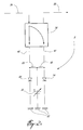
- FIG. 1 is a schematic block diagram of an illustrative embodiment of a predistorting linearizer channel amplifier according to the invention, with an agile bypass circuit;
- FIG. 2 a is a circuit diagram of a first illustrative embodiment of a voltage-controlled predistorter according to the present invention, forming part of a predistorting linearizer section of the predistorting linearizer channel amplifier of FIG. 1;
- FIG. 2 b is a circuit diagram of a second illustrative embodiment of a voltage-controlled predistorter according to the present invention, forming part of the predistorting linearizer section of the predistorting linearizer channel amplifier of FIG. 1;
- FIG. 2 c is a circuit diagram of a third illustrative embodiment of a voltage-controlled predistorter according to the present invention, forming part of the predistorting linearizer section of the predistorting linearizer channel amplifier of FIG. 1;
- FIG. 2 d is a circuit diagram of a fourth illustrative embodiment of a voltage-controlled predistorter according to the present invention, forming part of the predistorting linearizer section of the predistorting linearizer channel amplifier of FIG. 1;
- FIG. 2 e is a circuit diagram of a fifth illustrative embodiment of a voltage-controlled predistorter according to the present invention for use in the predistorting linearizer section of the predistorting linearizer channel amplifier of FIG. 1;
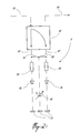
- FIG. 3 is a circuit diagram of an illustrative embodiment of a fault tolerant predistorting circuit and agile bypass including two predistorting linearizer sections and an agile bypass circuit;
- FIG. 4 a is a graph showing the input power (P in ) versus the output power (P out ) response of a non-linearized versus a linearized power amplifier;
- FIG. 4 b is a graph showing P in versus Phase response of a non-linearized versus a linearized solid-state power amplifier
- FIG. 4 c is a graph showing the W-CDMA spectrum of a non-linearized versus a linearized solid-state power amplifier
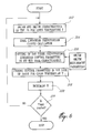
- FIG. 5 is an illustrative embodiment of a flow chart that can be used for the design of a predistorting linearizer channel amplifier in accordance with the present invention
- FIG. 6 is an illustrative embodiment of a flow chart that can be used for the alignment/calibration of a predistorting linearizer channel amplifier in accordance with the present invention
- FIG. 7 a is the frequency spectrum measured at the output of a TWTA (Travelling Wave Tube Amplifier) and a predistorted TWTA both driven by a 22 MHz QPSK signal;
- TWTA Travelling Wave Tube Amplifier
- FIG. 7 b is the frequency spectrum measured at the output of a TWTA and a predistorted TWTA both driven by a CDMA Multi carrier signal;
- FIG. 7 c is the frequency spectrum measured at the output of a TWTA and a predistorted TWTA both driven by a 2.4 MHz 16QAM signal;
- FIG. 7 d is the frequency spectrum measured at the output of a TWTA and a predistorted TWTA both driven by a 2.4 MHz BPSK signal;
- FIG. 8 a is a graph showing typical AM/AM curves for a predistorting linearizer channel amplifier with varying biasing voltages V p ;
- FIG. 8 b is a graph showing typical AM/AM curves for a predistorting linearizer channel amplifier with varying biasing voltages V a ;
- FIG. 8 c is a graph showing typical AM/AM curves for a predistorting linearizer channel amplifier illustrating the effect of varying both biasing voltages V p and V a ;
- FIG. 8 d is a graph showing typical AM/AM curves for both a predistorted and unpredistorted power amplifiers.
- FIG. 8 e is a graph showing typical AM/PM curves for both a predistorted and unpredistorted power amplifiers.
- the predistorting linearizer channel amplifier 200 principally comprises a predistorting linearizer section 2 and a predistortion controller 98 .
- An agile bypass can also be provided for. These will be described in detail herein below.
- the predistorting linearizer section 2 of the illustrative embodiment of FIG. 1 is a non-linear correcting circuit which intentionally introduces a predistortion in a signal, for example a high amplitude RF input signal 4 .
- This predistortion will cancel a distortion subsequently produced by a power amplifier 6 without compromising the efficiency of this power amplifier close to saturation.
- the high amplitude input signal 4 is a high crest factor modulated signal.
- the power amplifier 6 can be, for example, a Solid State Power Amplifier (SSPA) or a Travelling Wave Tube Amplifier (TWTA) although it will be apparent to those of ordinary skill in the art that the predistorting linearizer section 2 may be used with a variety of types of amplifiers.
- SSPA Solid State Power Amplifier
- TWTA Travelling Wave Tube Amplifier
- the predistorting linearizer section 2 comprises a controllable input variable-attenuator and drive-amplifier circuit including serially interconnected variable attenuator 10 and input drive amplifier 12 .
- the serially interconnected variable attenuator 10 and input drive amplifier 12 attenuate and amplify the input signal 4 , and this attenuated and amplified signal 37 is supplied to a predistorter 8 . In this manner, the amplitude of the input signal 4 is controlled to thereby control the moment when the predistorter 8 begins to compress or expand signal 37 .
- the predistorter 8 produces a non-linear distortion of the signal 37 from the input drive amplifier 12 and adjusts the total power compression or expansion of this signal 37 .
- the predistorter 8 includes Schottky diodes or terminated transistors (MESFET, BJT, HBT, PHMET etc.) requiring a minimum level of signal to proceed with compression or expansion of the signal.
- the predistortion introduced in terms of phase and amplitude varies in accordance with a controllable biasing voltage applied to the predistorter 8 .
- the predistorting linearizer section 2 also comprises a controllable output variable-attenuator and drive-amplifier circuit including serially interconnected variable attenuator 14 and drive amplifier 16 to match the output level range of the predistorter 8 to the input level range of the power amplifier 6 .
- the predistorting linearizer section 2 is controllable through the following three (3) components:
- the gain of the controllable input variable-attenuator and drive amplifier circuit including the serially interconnected variable attenuator 10 and drive amplifier circuit 12 referred to as the input gain;
- the gain of the controllable output variable-attenuator and drive-amplifier circuit including the serially interconnected variable attenuator 14 and drive amplifier circuit 16 referred to as the output gain
- VVA Variable Voltage Attenuator
- the predistorter 8 can comprise of a hybrid coupler 34 having a RF input 36 constituting the input of the predistorter 8 supplied with the attenuated and amplified RF signal 37 , a RF output 38 constituting the output of the predistorter 8 for supplying a predistorted version 39 of the RF signal 37 , a direct port 40 and a coupled port 42 .
- a first inductor 44 is connected between the direct port 40 and a controllable voltage source 46 .
- a second inductor 48 is connected between the coupled port 42 and the controllable biasing-voltage supply 46 .
- a first Schottky diode 50 has a cathode connected to the ground 52 and an anode connected to the direct port 40 .
- a second Schottky diode 54 has an anode connected to the coupled port 42 and a cathode connected to the ground 52 .
- the controllable biasing-voltage supply 46 supplies diodes 50 and 54 with a controllable biasing voltage via the inductors 44 and 48 , respectively.
- the predistorter 8 produces a controllable predistortion of the RF signal related to the controllable biasing voltage to cancel a distortion subsequently produced by the microwave power amplifier 6 .
- the first inductor 44 is connected between the direct port 40 and the controllale biasing-voltage source 46 .
- the second inductor 48 is connected between the coupled port 42 and the controllable biasing-voltage supply 46 .
- Schottky diodes 56 and 58 are connected in a head-to-tail configuration between the direct port 40 and the ground 52 .
- Schottky diodes 60 and 62 are connected in a head-to-tail configuration between the coupled port 42 and the ground 52 .
- the controllable biasing-voltage supply 46 is connected via the first and second inductors 44 and 48 to the direct port 40 and the coupled port 42 , respectively, thereby supplying the diodes 56 , 58 and 60 , 62 with a controllable biasing voltage.
- the predistorter 8 produces a controllable predistortion of the RF signal 37 related to the controllable biasing voltage to cancel a distortion subsequently produced by the microwave power amplifier 6 .
- the first inductor 44 is connected between the direct port 40 and the controllable voltage source 46 .
- the second inductor 48 is connected between the coupled port 42 and the controllable biasing-voltage supply 46 .
- a line matching circuit 64 is connected between the direct port 42 and the anode of a first Schottky diode 66 .
- a line matching circuit 68 is connected between the coupled port 42 and the anode of a second Schottky diode 70 . Both the first and second Schottky diodes 66 and 70 have their cathodes connected to the ground 52 .
- the controllable biasing-voltage supply 46 supplies the diodes 66 and 70 with a controllable biasing voltage.
- the predistorter 8 produces a controllable predistortion of the RF signal 37 related to the controllable biasing voltage to cancel a distortion subsequently produced by the microwave power amplifier 6 .
- the first inductor 44 is connected between the direct port 40 and the controllable voltage source 46 .
- the second inductor 48 is connected between the coupled port 42 and the controllable biasing-voltage supply 46 .
- First and second Schottky diodes 72 and 74 have their cathodes connected to the ground 52 .
- a first line matching circuit 76 is interposed between the anode of the diode 72 and the direct port 40 .
- third and fourth Schottky diodes 78 and 80 have their cathodes connected to the ground 52 .
- a second line matching circuit 82 is interposed between the anode of the diode 78 and the coupled port 42 .
- the controllable biasing-voltage supply 46 supplies diodes 72 , 74 , 78 and 80 with a controllable biasing voltage.
- two terminated biased transistors 84 and 86 are connected between the direct port 40 or coupled port 42 and the ground 52 . More specifically the source of the first transistor 84 is connected to the direct port 40 and the drain of the first transistor 84 is connected to the ground 52 . Similarly, the source of the second transistor 86 is connected to the coupled port 42 and the drain of the second transistor 86 is connected to the ground 52 .
- the controllable biasing-voltage supply 46 is connected to the gates of the first and second transistors 84 and 86 thereby supplying both transistors with a controllable biasing voltage.
- the predistorter 8 still produces a controllable predistortion of the RF signal 37 related to the controllable biasing voltage to cancel a distortion subsequently produced by the microwave power amplifier 6 .
- the transistors 84 and 86 can be terminated transistors selected from the group consisting of: MESFET transistors; BJT transistors, HBT transistors; PHMET transistors; etc.
- the choice of a predistorter configuration depends on the kind of power amplifier 6 for which the input signal 4 is to be predistorted.
- An initial criterion is the total gain distortion (compression or expansion, AM/AM distortion) and phase shift variation (advance or lag, AM/PM distortion) of the power amplifier 6 .
- the adjustment of the predistorter parameters is required to fit the ideal predistortion curves as detailed below.
- gain and phase may be distorted through controllable biasing of the attenuators 10 and 14 and the predistorter 8 .
- Controllable biasing of these circuits is carried out though control of the controllable biasing-voltage supply 46 .
- FIG. 8 a shows curves representing the normalised ratio of the amplitude of the output signal 39 of the predistorter 8 over the amplitude of the input signal 37 to the predistorter 8 (AM/AM) versus the input power P in .
- This property of the predistorter can be used as a software bypass by setting the biasing voltage V p below an operational threshold, typically 0V. In this condition the predistorter does not produce a controllable predistortion (i.e. it does not expand the input signal) over a wide input drive level P in .
- FIG. 8 b illustrates curves representing the ratio of the normalised amplitude of the input signal to the power amplifier 6 over the amplitude of the input signal 37 to the predistorter (AM/AM) versus the input power P in .
- FIG. 8 c this Figure illustrates curves representing the normalised ratio of the amplitude of the input signal to the power amplifier 6 over the amplitude of the input signal 4 (AM/AM) versus the input power P in .
- curves representing the normalised ratio of the amplitude of the output signal from the power amplifier 6 over the amplitude of the input signal 4 (AM/AM) versus the input power P in are disclosed for both predistorted and unpredistorted signals.
- the non-predistorted power amplifier 6 begins to compress input signals, thereby causing the output power to decrease nonlinearly relative to the input power. Further increase in P in eventually causes the amplifier to saturate at P 1 .
- the amplified output signal remains in a linear relationship with the input signal at higher input signal amplitudes.
- single values of V p and V a are necessary to insure adequate predistortion.
- FIG. 8 e show curves representing a typical input power versus output phase shift (AM/PM) for a predistorted and non-predistorted power amplifier 6 . Similar to the amplitude of the output signal from the power amplifier 6 , as the input power P in is steadily increased eventually the power amplifier 6 begins to saturate causing the output signal to be phase-shifted relative to the input signal. Referring back to FIG. 8 d in addition to FIG. 8 e , by raising accordingly the voltage V p of the controllable biasing-voltage supply 46 of the predistorter 8 as disclosed in FIGS.
- the phase of the input signal can be shaped to compensate for the non-linear phase shift variation of the power amplifier 6 such that the phase of the output signal from the power amplifier 6 remains in a steady relationship with the phase of the input signal 4 at higher input signal amplitudes.
- communication systems and in particular those which are satellite based generally have additional requirements in terms of increased tolerance to faults which must be met before the system can be placed in full service.
- an agile bypass 86 is included which allows the predistorting linearizer section 2 to be bypassed in cases of fault or failure of the predistorting linearizer section 2 including the attenuator 10 , the input drive amplifier 12 , the predistorter 8 , the attenuator 14 and the output drive amplifier 16 .
- the predistorting linearizer section 2 is inactive for input signals 4 of amplitudes which would not drive the power amplifier 6 into compression, and therefore the predistorting linearizer section 2 may also be bypassed using the agile bypass 86 under such circumstances.
- the agile bypass 86 comprises an input switch 88 , an output switch 90 and a circuit formed by a compensation amplifier 92 such that a small signal gain of the agile bypass circuit equals a small signal gain of the predistortion circuit.
- An input signal detector 94 and output signal detector 96 complete the circuit.
- Control of the input switch 88 and the output switch 90 is provided by the controller circuit 98 via a control line 100 and a control line 102 , respectively.
- the decision to use the agile bypass 86 is based on (i) the level of the input signal 4 as detected by the input signal detector 94 and supplied to the controller circuit 98 via line 104 , and (ii) the level of the output signal 106 from the output drive amplifier 16 as detected by the output signal detector 96 and supplied to the controller circuit 98 via line 108 .
- a processor 110 of the controller circuit 98 detects a failure of the predistorting linearizer section 2 and therefore decides to use the agile bypass 86 on the basis of a comparison of the signal levels measured through the input signal detector 94 , the output signal detector 96 , a signal conditioner 120 and a digital-to-analog (D/A) converter 118 .
- a pre-calibrated value for example 5 dB
- a fault condition will be assumed to have been detected and the predistorting linearizer section 2 bypassed through the agile bypass 86 .
- the difference between levels may vary with the temperature of operation of the power amplifier 6 and therefore values must be pre-calibrated for the range of temperatures of operation.
- a plurality of predistorting linearizer channel amplifiers such as 300 and 400 are provided together with suitable input and output switches 88 and 90 .
- a controller 98 provides for the predistorting linearizer channel amplifiers 300 or 400 to be hot swapped in instances of failure or maintenance without affecting the performance of the predistortion.
- the predistorting linearizer section 2 needs to follow changes in the amplifier 6 due to a variation in temperature in order to maintain the linearity of the system and therefore its overall performance.
- the controller circuit 98 is provided.
- the controller circuit 98 comprises the processor 110 (CPU), a look-up table 112 stored in memory banks 114 , an external interface 116 , the digital-to-analog (D/A) converter 118 , and the signal conditioner 120 .
- a vector signal analyser (not shown) is used to measure the normalised gain versus the input power P in and the normalised phase shift versus the input power P in of the non-linearized power amplifier (see the curves in dashed line of FIGS. 4 a and 4 b ). From the measured AM/AM and AM/PM curves of FIGS.
- a PC Personal Computer
- a PC can be programmed for calculating ideal predistortion curves and corresponding predistortion control parameters to be applied to the predistorting linearizer section 2 in order to obtain the AM/AM or AM/PM curves closest to the ideal curves illustrated in solid lines in FIGS. 4 a and 4 b.
- the problem of predistorting the input signal of the power amplifier 6 is essentially a complex curve-fitting problem having as objective function the complex gain of an ideal limiter for the power amplifier, not only as a problem of minimising the third order inter-modulation distortion products.
- the derived predistortion control parameters are stored in the look-up table 112 for different temperatures of operation of the power amplifier 6 .
- the predistortion control parameters stored in the look-up table 112 are suitable for controlling through the D/A converter 118 and the signal conditioner 120 , the variable attenuator 10 through line 122 , the variable attenuator 14 through line 124 and the controllable biasing-voltage supply 46 through line 126 . This allows the predistorting linearizer section 2 to compensate for the non-linearities of a wide range of power amplifiers over a wide range of environmental conditions.
- Signal conditioner 120 is in fact a buffer circuit for interfacing the voltage level at the output of the D/A converter 118 with the voltage level of the diodes (or transistors) of the attenuators 10 and 14 and the predistorter 8 , protecting both the D/A converter 118 and the diodes (or transistors).
- FIG. 5 is a flow chart of an illustrative procedure for designing a predistorting linearizer channel amplifier 200 (FIG. 1).
- the first step 202 of this design procedure is to measure the AM/AM and AM/PM characteristics of the power amplifier 6 . This can be done, for example, by analysing the power amplifier 6 with a Vector Network Analyser (VNA) while subjecting the power amplifier 6 to a variety of input signals and amplitudes.
- VNA Vector Network Analyser
- ideal linearizer predistortion curves are calculated.
- the ideal linearizer predistortion curves are generally represented as the inverse of AM/AM and AM/PM curves normalised relative to the small signal gain.
- a user can choose (step 208 ) the configuration of the predistorter 8 from, for example, those proposed in FIGS. 2 a to 2 e .
- predistorter 8 comprising diodes (FIGS. 2 a - 2 d ) produces the desired results. If the slope in the AM/AM curve is abrupt, predistorter circuits of FIGS. 2 a - 2 c will be chosen. If the slope is not abrupt, the predistorter circuit of FIG. 2 d will provide a better choice. For a power amplifier 6 showing more than one inflection point in its AM/AM curve (usually seen in SSPAs), predistorter 8 circuits comprising transistors (FIG. 2 e ) produce desired results.
- step 210 optimization of the design of the RF components of the predistorting linearizer section 2 (i.e., the predistorter 8 and its components (see FIGS. 2 a to 2 e ); the attenuators 10 and 14 and their components and the amplifiers 12 and 16 (see FIG. 1)) is conducted in order to synthesise the characteristics closest to the ideal predistortion curves over the required temperature range is carried out.
- FIG. 6 is a block diagram of the alignment/calibration procedure of the predistorting linearizer channel amplifier 200 .
- the first step 212 in the alignment/calibration of the linearizer channel amplifier 200 consists of measuring the AM/AM and AM/PM characteristics of the power amplifier 6 for an initial temperature T i .
- the initial temperature T i (for example, the lowest temperature of a given temperature range) as well as T max (for example, the highest temperature of the given temperature range) are chosen on the basis of the particular temperature specifications in which the predistorter will be used.
- the temperature range could be, as a non limitative example, ⁇ 30° C. to 80° C. for military applications.
- ideal linearizer predistortion curves are calculated based on the measured AM/AM and AM/PM curves.
- the ideal linearizer predistortion curves are generally represented as the inverse of these measured AM/AM and AM/PM curves.
- step 218 the control parameters for T i are stored in look-up table 112 . Temperature T i is then incremented (step 220 ) and, at step 222 , it is determined whether T max is reached. If it is not, the alignment/calibration procedure continues, returns to step 212 , and performs the subsequent steps with a new temperature value T. When T max is reached, the procedure stops.
- steps 220 and 222 are possible.
- the initial temperature T i could be the highest temperature of the temperature range and the temperature could be decremented until T min is reached.
- the temperature increments (step 220 ) could take on different values for each iteration depending on the rate of change, in relation to the change in temperature, of the AM/AM and AM/PM curves.
- the processor (CPU) 110 measures the temperature T p of the power amplifier through the signal conditioner 120 and the D/A converter 118 , selects predistortion control parameters from the look-up table 112 in relation to the measured temperature, and finally applies these predistortion parameters to the variable attenuators 10 and 14 and the predistorter 8 to linearize the output signal of the power amplifier 6 , i.e. to produce a predistorted output signal 106 which cancels the distortion subsequently produced by the microwave power amplifier 6 .
- controller circuit 98 the function of the controller circuit 98 is to provide a set of predistortion control parameters for controlling the biasing voltages V a of the attenuators 10 and 14 , and the biasing voltage V p of the predistorter 8 in relation to the temperature of operation of the power amplifier 6 .
- Controller circuit 98 can be a FPGA (Fast Programmable Gate Array), a DSP (Digital Signal Processor) or a PIC (Programmable Integrated Controller), etc., and can be interfaced with a PC (Personal Computer) through the external interface 116 to automatically adjust the predistortion curves directly.
- PC Personal Computer
- the processor 110 may include a program that tries to maintain good linearity of the linearized power amplifier 6 over a wide range of environmental conditions, operating conditions or type of input signals (for example CDMA, QPSK, BPSK, nQAM, etc.).
- application of the concept of the present invention is not limited to microwave power amplifiers but to any other type of amplifier requiring compensation for environmental conditions affecting distortion produced by the amplifier, and therefore linearity of the amplifier.
Abstract
Description
- The present invention relates to a voltage-controlled predistorter that can be used in a predistorting linearizer. The function of the predistorter is to predistort an input signal in view of cancelling a distortion subsequently produced by an amplifier.
- Microwave power amplifiers (solid state or travelling wave amplifiers) used in ground station transmitters and communication satellites should ideally be highly efficient and provide linear amplification over a wide range of input power. Obviously, the performance of these microwave power amplifiers is limited by the non-linearities of their inner parts or constituents. A wide variety of correction methods for a microwave power amplifier's non-linearities have been proposed and implemented including power back-off, negative feedback, feed forward, etc. However, in most cases the efficiency of the linearized amplifier drops significantly with respect to the efficiency of the non-linearized amplifier specially when the amplifier input is a high crest factor modulated signal such as a CDMA (Code Division Multiple Access), NPR (Noise Power Ratio), or other types of signals.
- Predistortion is one of the best cost-effective approaches to reduce the level of non-linear distortion generated by microwave power amplifiers while retaining relatively good power efficiency. Predistortion consists of introducing in the input microwave signal amplitude and phase distortion opposite to the distortion produced by the microwave power amplifier. In this manner, distortion is cancelled to obtain at the output of the power amplifier a signal that is an amplified replica of the input signal with almost no power efficiency decrease. Therefore, the function of a predistorter is to generate both inverse amplitude and phase non-linearity. Since the characteristics of a microwave power amplifier significantly change with temperature, the predistorter has to maintain the overall performance of linearity of the system and to follow the amplifier changes.
- An object of the present invention is therefore to provide a predistorter for use in conjunction with an amplifier for predistorting an input signal in view of cancelling signal distortion subsequently produced by the amplifier.
- More specifically, In accordance with the present invention, there is provided a predistorter for predistorting a RF signal subsequently injected in an amplifier, comprising:
- a hybrid coupler comprising a RF input constituting an input of the predistorter supplied with the RF signal, a RF output constituting an output of the predistorter for supplying a predistorted version of the RF signal, a direct port, and a coupled port;
- a first semiconductor component connected between the direct port and the ground;
- a second semiconductor component connected between the coupled port and the ground; and
- a controllable biasing-voltage supply connected to the first and second semiconductor components, thereby supplying the first and second semiconductor components with a controllable biasing voltage.
- In operation, the predistorter produces a controllable predistortion of the RF signal related to the controllable biasing voltage to cancel a distortion subsequently produced by the amplifier.
- In accordance with the present invention, there is also provided a predistorting linearizer channel amplifier for processing a RF signal subsequently injected in an amplifier, comprising:
- a controllable input variable-attenuator and drive-amplifier circuit supplied with the RF signal to attenuate and amplify the RF signal;
- the above described predistorter supplied with the attenuated and amplified RF signal to produce a predistorted RF signal;
- a controllable output variable-attenuator and drive-amplifier circuit supplied with the predistorted RF signal to attenuate and amplify the predistorted RF signal before supply of the predistorted RF signal to the amplifier; and
- a controller connected to the controllable input variable-attenuator and drive-amplifier circuit, the biasing-voltage supply, and the controllable output variable-attenuator and drive-amplifier circuit, this controller embodying a phase-shifting and amplitude-adjusting control function applied to the controllable input variable-attenuator and drive-amplifier circuit, the controllable biasing-voltage supply, and the controllable output variable-attenuator and drive-amplifier circuit in order to produce a predistortion of the RF signal which cancels a distortion subsequently produced by the amplifier.
- In accordance with the present invention, there is also provided a predistorter for predistorting a RF signal subsequently injected in an amplifier, comprising:
- a hybrid coupler comprising a RF input constituting an input of the predistorter supplied with the RF signal, a RF output constituting an output of the predistorter for supplying a predistorted version of the RF signal, a direct port, and a coupled port;
- a first diode having an anode connected to the direct port and a cathode connected to the ground;
- a second diode having an anode connected to the coupled port and a cathode connected to the ground; and
- a controllable biasing-voltage supply connected to the direct port and to the coupled port, thereby supplying the direct and coupled ports with a controllable biasing voltage.
- In operation, the predistorter produces a controllable predistortion of the RF signal related to the controllable biasing voltage to cancel a distortion subsequently produced by the amplifier.
- In accordance with the present invention, there is further provided a predistorter for predistorting a RF signal subsequently injected in an amplifier, comprising:
- a hybrid coupler comprising a RF input constituting an input of the predistorter supplied with the RF signal, a RF output constituting an output of the predistorter for supplying a predistorted version of the RF signal, a direct port, and a coupled port;
- first and second diodes connected between the direct port and the ground, the first and second diodes being connected in head to tail configuration;
- third and fourth diodes connected between the direct port and the ground, the third and fourth diodes being connected in head to tail configuration; and
- a controllable biasing-voltage supply connected to the direct port and to the coupled port, thereby supplying the direct and coupled ports with a controllable biasing voltage.
- In operation, the predistorter produces a controllable predistortion of the RF signal related to the controllable biasing voltage to cancel a distortion subsequently produced by the amplifier.
- The present invention still further relates to a predistorter for predistorting a RF signal subsequently injected in an amplifier, comprising:
- a hybrid coupler comprising a RF input constituting an input of the predistorter supplied with the RF signal, a RF output constituting an output of the predistorter for supplying a predistorted version of the RF signal, a direct port, and a coupled port;
- a first diode having an anode connected to the direct port and a cathode connected to the ground;
- a first matching circuit and a second diode connected in series between the direct port and the ground, the second diode having a cathode connected to the ground;
- a third diode having an anode connected to the coupled port and a cathode connected to the ground;
- a second matching circuit and a fourth diode connected in series between the coupled port and the ground, the fourth diode having a cathode connected to the ground; and
- a controllable biasing-voltage supply connected to the direct port and the coupled port, thereby supplying the direct and coupled ports with a controllable biasing voltage.
- In operation, the predistorter produces a controllable predistortion of the RF signal related to the controllable biasing voltage to cancel a distortion subsequently produced by the amplifier.
- Still in accordance with the present invention, there is provided a predistorter for predistorting a RF signal subsequently injected in an amplifier, comprising:
- a hybrid coupler comprising a RF input constituting an input of the predistorter supplied with the RF signal, a RF output constituting an output of the predistorter for supplying a predistorted version of the RF signal, a direct port, and a coupled port;
- a first transistor connected between the direct port and the ground;
- a second transistor connected between the coupled port and the ground; and
- a controllable biasing-voltage supply connected to the first transistor and the second transistor, thereby supplying the first and second transistors with a controllable biasing voltage.
- In operation, the predistorter produces a controllable predistortion of the RF signal related to the controllable biasing voltage to cancel a distortion subsequently produced by the amplifier.
- According to the present invention, there is further provided a predistorting linearizer channel amplifier for processing an input signal subsequently supplied to a power amplifier, comprising:
- a controllable input variable-attenuator and drive-amplifier circuit supplied with the input signal to attenuate and amplify the input signal;
- a predistorter comprising a controllable phase-shifting and amplitude-adjusting path supplied with the attenuated and amplified input signal to distort the attenuated and amplified input signal and produce a predistorted output signal;
- a controllable output variable-attenuator and drive-amplifier circuit supplied with the predistorted output signal to attenuate and amplify the predistorted output signal before supplying the predistorted output signal to the power amplifier;
- a phase-shifting and amplitude-adjusting controller connected to the controllable input variable-attenuator and drive-amplifier circuit, the controllable phase-shifting a n d amplitude-adjusting path, and the controllable output variable-attenuator and drive-amplifier circuit; and
- a bypass extending in parallel with the series circuit including the serially interconnected input variable-attenuator and drive-amplifier circuit, controllable phase-shifting and amplitude-adjusting path, and output variable-attenuator and drive-amplifier circuit, the bypass defining a bypass circuit established in response to a fault condition in the series circuit to bypass the faulty series circuit.
- The foregoing and other objects, advantages and features of the present invention will become more apparent upon reading of the following non-restrictive description of illustrative embodiments thereof, given by way of example only with reference to the accompanying drawings.
- In the appended drawings:
- FIG. 1 is a schematic block diagram of an illustrative embodiment of a predistorting linearizer channel amplifier according to the invention, with an agile bypass circuit;
- FIG. 2 a is a circuit diagram of a first illustrative embodiment of a voltage-controlled predistorter according to the present invention, forming part of a predistorting linearizer section of the predistorting linearizer channel amplifier of FIG. 1;
- FIG. 2 b is a circuit diagram of a second illustrative embodiment of a voltage-controlled predistorter according to the present invention, forming part of the predistorting linearizer section of the predistorting linearizer channel amplifier of FIG. 1;
- FIG. 2 c is a circuit diagram of a third illustrative embodiment of a voltage-controlled predistorter according to the present invention, forming part of the predistorting linearizer section of the predistorting linearizer channel amplifier of FIG. 1;
- FIG. 2 d is a circuit diagram of a fourth illustrative embodiment of a voltage-controlled predistorter according to the present invention, forming part of the predistorting linearizer section of the predistorting linearizer channel amplifier of FIG. 1;
- FIG. 2 e is a circuit diagram of a fifth illustrative embodiment of a voltage-controlled predistorter according to the present invention for use in the predistorting linearizer section of the predistorting linearizer channel amplifier of FIG. 1;
- FIG. 3 is a circuit diagram of an illustrative embodiment of a fault tolerant predistorting circuit and agile bypass including two predistorting linearizer sections and an agile bypass circuit;
- FIG. 4 a is a graph showing the input power (Pin) versus the output power (Pout) response of a non-linearized versus a linearized power amplifier;
- FIG. 4 b is a graph showing Pin versus Phase response of a non-linearized versus a linearized solid-state power amplifier;
- FIG. 4 c is a graph showing the W-CDMA spectrum of a non-linearized versus a linearized solid-state power amplifier;
- FIG. 5 is an illustrative embodiment of a flow chart that can be used for the design of a predistorting linearizer channel amplifier in accordance with the present invention;
- FIG. 6 is an illustrative embodiment of a flow chart that can be used for the alignment/calibration of a predistorting linearizer channel amplifier in accordance with the present invention;
- FIG. 7 a is the frequency spectrum measured at the output of a TWTA (Travelling Wave Tube Amplifier) and a predistorted TWTA both driven by a 22 MHz QPSK signal;
- FIG. 7 b is the frequency spectrum measured at the output of a TWTA and a predistorted TWTA both driven by a CDMA Multi carrier signal;
- FIG. 7 c is the frequency spectrum measured at the output of a TWTA and a predistorted TWTA both driven by a 2.4 MHz 16QAM signal;
- FIG. 7 d is the frequency spectrum measured at the output of a TWTA and a predistorted TWTA both driven by a 2.4 MHz BPSK signal;
- FIG. 8 a is a graph showing typical AM/AM curves for a predistorting linearizer channel amplifier with varying biasing voltages Vp;
- FIG. 8 b is a graph showing typical AM/AM curves for a predistorting linearizer channel amplifier with varying biasing voltages Va;
- FIG. 8 c is a graph showing typical AM/AM curves for a predistorting linearizer channel amplifier illustrating the effect of varying both biasing voltages Vp and Va;
- FIG. 8 d is a graph showing typical AM/AM curves for both a predistorted and unpredistorted power amplifiers; and
- FIG. 8 e is a graph showing typical AM/PM curves for both a predistorted and unpredistorted power amplifiers.
- Referring to FIG. 1, the predistorting
linearizer channel amplifier 200 principally comprises apredistorting linearizer section 2 and apredistortion controller 98. An agile bypass can also be provided for. These will be described in detail herein below. - (a) The Predistorting Linearizer Section
- The
predistorting linearizer section 2 of the illustrative embodiment of FIG. 1 is a non-linear correcting circuit which intentionally introduces a predistortion in a signal, for example a high amplitudeRF input signal 4. This predistortion will cancel a distortion subsequently produced by apower amplifier 6 without compromising the efficiency of this power amplifier close to saturation. In the illustrative embodiment of FIG. 1, the highamplitude input signal 4 is a high crest factor modulated signal. Thepower amplifier 6 can be, for example, a Solid State Power Amplifier (SSPA) or a Travelling Wave Tube Amplifier (TWTA) although it will be apparent to those of ordinary skill in the art that thepredistorting linearizer section 2 may be used with a variety of types of amplifiers. - The
predistorting linearizer section 2 comprises a controllable input variable-attenuator and drive-amplifier circuit including serially interconnectedvariable attenuator 10 andinput drive amplifier 12. The serially interconnectedvariable attenuator 10 andinput drive amplifier 12 attenuate and amplify theinput signal 4, and this attenuated and amplifiedsignal 37 is supplied to apredistorter 8. In this manner, the amplitude of theinput signal 4 is controlled to thereby control the moment when thepredistorter 8 begins to compress or expandsignal 37. - The
predistorter 8 produces a non-linear distortion of thesignal 37 from theinput drive amplifier 12 and adjusts the total power compression or expansion of thissignal 37. As will be seen in the following description, thepredistorter 8 includes Schottky diodes or terminated transistors (MESFET, BJT, HBT, PHMET etc.) requiring a minimum level of signal to proceed with compression or expansion of the signal. The predistortion introduced in terms of phase and amplitude varies in accordance with a controllable biasing voltage applied to thepredistorter 8. - Since the output power at saturation of the non-predistorted power amplifier (PA) 6 and the predistorted power amplifier (PPA) 6 must be substantially the same, the
predistorting linearizer section 2 also comprises a controllable output variable-attenuator and drive-amplifier circuit including serially interconnectedvariable attenuator 14 and driveamplifier 16 to match the output level range of thepredistorter 8 to the input level range of thepower amplifier 6. - Therefore, in view of the above description, the
predistorting linearizer section 2 is controllable through the following three (3) components: - the gain of the controllable input variable-attenuator and drive amplifier circuit including the serially interconnected
variable attenuator 10 and driveamplifier circuit 12, referred to as the input gain; - the gain of the controllable output variable-attenuator and drive-amplifier circuit including the serially interconnected
variable attenuator 14 and driveamplifier circuit 16, referred to as the output gain; and - the biasing voltage of the
predistorter 8. - (a.1) The Attenuators
- The attenuators are well known in the art and may be purchased of the shelf, for example as Variable Voltage Attenuator (VVA) available from all major RF equipment manufacturers. They will not be discussed here.
- (a.2) The Predistorter
- As shown in FIGS. 2 a, 2 b, 2 c, 2 d and 2 e, when the
power amplifier 6 is a microwave power amplifier, thepredistorter 8 can comprise of ahybrid coupler 34 having aRF input 36 constituting the input of thepredistorter 8 supplied with the attenuated and amplifiedRF signal 37, aRF output 38 constituting the output of thepredistorter 8 for supplying apredistorted version 39 of theRF signal 37, adirect port 40 and a coupledport 42. - In the example of FIG. 2 a, a
first inductor 44 is connected between thedirect port 40 and acontrollable voltage source 46. Asecond inductor 48 is connected between the coupledport 42 and the controllable biasing-voltage supply 46. Afirst Schottky diode 50 has a cathode connected to theground 52 and an anode connected to thedirect port 40. Asecond Schottky diode 54 has an anode connected to the coupledport 42 and a cathode connected to theground 52. The controllable biasing-voltage supply 46supplies diodes inductors predistorter 8 produces a controllable predistortion of the RF signal related to the controllable biasing voltage to cancel a distortion subsequently produced by themicrowave power amplifier 6. - Referring now to FIG. 2 b, the
first inductor 44 is connected between thedirect port 40 and the controllale biasing-voltage source 46. Thesecond inductor 48 is connected between the coupledport 42 and the controllable biasing-voltage supply 46.Schottky diodes direct port 40 and theground 52.Schottky diodes port 42 and theground 52. The controllable biasing-voltage supply 46 is connected via the first andsecond inductors direct port 40 and the coupledport 42, respectively, thereby supplying thediodes predistorter 8 produces a controllable predistortion of theRF signal 37 related to the controllable biasing voltage to cancel a distortion subsequently produced by themicrowave power amplifier 6. - In the example of FIG. 2 c, the
first inductor 44 is connected between thedirect port 40 and thecontrollable voltage source 46. Thesecond inductor 48 is connected between the coupledport 42 and the controllable biasing-voltage supply 46. Aline matching circuit 64 is connected between thedirect port 42 and the anode of afirst Schottky diode 66. Similarly, aline matching circuit 68 is connected between the coupledport 42 and the anode of asecond Schottky diode 70. Both the first andsecond Schottky diodes ground 52. Via the first andsecond inductors line matching circuits voltage supply 46 supplies thediodes - In operation, the
predistorter 8 produces a controllable predistortion of theRF signal 37 related to the controllable biasing voltage to cancel a distortion subsequently produced by themicrowave power amplifier 6. - Referring now to FIG. 2 d, the
first inductor 44 is connected between thedirect port 40 and thecontrollable voltage source 46. Thesecond inductor 48 is connected between the coupledport 42 and the controllable biasing-voltage supply 46. First andsecond Schottky diodes ground 52. A firstline matching circuit 76 is interposed between the anode of thediode 72 and thedirect port 40. Similarly, third andfourth Schottky diodes ground 52. A secondline matching circuit 82 is interposed between the anode of thediode 78 and the coupledport 42. Via the first andsecond inductors voltage supply 46supplies diodes - Finally, in the embodiment of FIG. 2 e, two terminated
biased transistors direct port 40 or coupledport 42 and theground 52. More specifically the source of thefirst transistor 84 is connected to thedirect port 40 and the drain of thefirst transistor 84 is connected to theground 52. Similarly, the source of thesecond transistor 86 is connected to the coupledport 42 and the drain of thesecond transistor 86 is connected to theground 52. The controllable biasing-voltage supply 46 is connected to the gates of the first andsecond transistors - In operation, the
predistorter 8 still produces a controllable predistortion of theRF signal 37 related to the controllable biasing voltage to cancel a distortion subsequently produced by themicrowave power amplifier 6. - The
transistors - The choice of a predistorter configuration depends on the kind of
power amplifier 6 for which theinput signal 4 is to be predistorted. An initial criterion is the total gain distortion (compression or expansion, AM/AM distortion) and phase shift variation (advance or lag, AM/PM distortion) of thepower amplifier 6. The adjustment of the predistorter parameters is required to fit the ideal predistortion curves as detailed below. - In the
predistorting linearizer section 2, gain and phase may be distorted through controllable biasing of theattenuators predistorter 8. Controllable biasing of these circuits is carried out though control of the controllable biasing-voltage supply 46. - FIG. 8 a shows curves representing the normalised ratio of the amplitude of the
output signal 39 of thepredistorter 8 over the amplitude of theinput signal 37 to the predistorter 8 (AM/AM) versus the input power Pin. By increasing the biasing voltage Vp of the controllable biasing-voltage supply 46 of thepredistorter 8 as disclosed in FIGS. 2a-e, the input signal is expanded at a lower drive level (input power), causing the ratio of the normalised amplitude of theoutput signal 39 over the amplitude of theinput signal 37 to increase as shown in FIG. 8a. - This property of the predistorter can be used as a software bypass by setting the biasing voltage V p below an operational threshold, typically 0V. In this condition the predistorter does not produce a controllable predistortion (i.e. it does not expand the input signal) over a wide input drive level Pin.
- FIG. 8 b illustrates curves representing the ratio of the normalised amplitude of the input signal to the
power amplifier 6 over the amplitude of theinput signal 37 to the predistorter (AM/AM) versus the input power Pin. By increasing the biasing voltage Va to thevariable attenuator 14 the power level Pin at which the input signal to thepower amplifier 6 begins to stray from theinput signal 37 to the predistorter 8 (referred to as the “knee” on the diagram) can be adjusted. - Referring now to FIG. 8 c, this Figure illustrates curves representing the normalised ratio of the amplitude of the input signal to the
power amplifier 6 over the amplitude of the input signal 4 (AM/AM) versus the input power Pin. By combining the effects of the biasing voltage Vp to thepredistorter 8 and the biasing voltage Va to thevariable attenuator 14 the input signal to thepower amplifier 6 can be optimally predistorted to compensate for distortion introduced by thepower amplifier 6 at high amplitudes. - Referring now to FIG. 8 d, curves representing the normalised ratio of the amplitude of the output signal from the
power amplifier 6 over the amplitude of the input signal 4 (AM/AM) versus the input power Pin are disclosed for both predistorted and unpredistorted signals. At input power level P0 thenon-predistorted power amplifier 6 begins to compress input signals, thereby causing the output power to decrease nonlinearly relative to the input power. Further increase in Pin eventually causes the amplifier to saturate at P1. By driving the power amplifier with a predistorted signal, the amplified output signal remains in a linear relationship with the input signal at higher input signal amplitudes. Typically, for a givenpower amplifier 6 operating at a given temperature, single values of Vp and Va are necessary to insure adequate predistortion. - FIG. 8 e show curves representing a typical input power versus output phase shift (AM/PM) for a predistorted and
non-predistorted power amplifier 6. Similar to the amplitude of the output signal from thepower amplifier 6, as the input power Pin is steadily increased eventually thepower amplifier 6 begins to saturate causing the output signal to be phase-shifted relative to the input signal. Referring back to FIG. 8d in addition to FIG. 8e, by raising accordingly the voltage Vp of the controllable biasing-voltage supply 46 of thepredistorter 8 as disclosed in FIGS. 2a-e, the phase of the input signal can be shaped to compensate for the non-linear phase shift variation of thepower amplifier 6 such that the phase of the output signal from thepower amplifier 6 remains in a steady relationship with the phase of theinput signal 4 at higher input signal amplitudes. - (b) The Bypass Circuit
- Referring back to FIG. 1, communication systems and in particular those which are satellite based generally have additional requirements in terms of increased tolerance to faults which must be met before the system can be placed in full service. In order to meet these requirements an
agile bypass 86 is included which allows thepredistorting linearizer section 2 to be bypassed in cases of fault or failure of the predistorting linearizersection 2 including theattenuator 10, theinput drive amplifier 12, thepredistorter 8, theattenuator 14 and theoutput drive amplifier 16. Alternatively, since thepower amplifier 6 operates linearly when operated with low input signal levels, thepredistorting linearizer section 2 is inactive forinput signals 4 of amplitudes which would not drive thepower amplifier 6 into compression, and therefore thepredistorting linearizer section 2 may also be bypassed using theagile bypass 86 under such circumstances. - According to the example of FIG. 1, the
agile bypass 86 comprises aninput switch 88, anoutput switch 90 and a circuit formed by acompensation amplifier 92 such that a small signal gain of the agile bypass circuit equals a small signal gain of the predistortion circuit. Aninput signal detector 94 andoutput signal detector 96 complete the circuit. - Control of the
input switch 88 and theoutput switch 90 is provided by thecontroller circuit 98 via acontrol line 100 and acontrol line 102, respectively. The decision to use theagile bypass 86 is based on (i) the level of theinput signal 4 as detected by theinput signal detector 94 and supplied to thecontroller circuit 98 vialine 104, and (ii) the level of theoutput signal 106 from theoutput drive amplifier 16 as detected by theoutput signal detector 96 and supplied to thecontroller circuit 98 vialine 108. - For example, a
processor 110 of thecontroller circuit 98 detects a failure of the predistorting linearizersection 2 and therefore decides to use theagile bypass 86 on the basis of a comparison of the signal levels measured through theinput signal detector 94, theoutput signal detector 96, asignal conditioner 120 and a digital-to-analog (D/A)converter 118. When the difference between the levels is not substantially equal to a pre-calibrated value, for example 5 dB, a fault condition will be assumed to have been detected and thepredistorting linearizer section 2 bypassed through theagile bypass 86. Note that the difference between levels may vary with the temperature of operation of thepower amplifier 6 and therefore values must be pre-calibrated for the range of temperatures of operation. - Although in the present illustrative embodiment the amplitudes of the input and output signal levels have been compared in order to detect a fault condition, it will be apparent to those of ordinary skill in the art that other attributes of the input and output signal could be detected and compared in order to determine the presence of a fault in the
predistorting linearizer circuit 2. - Referring now to FIG. 3, in a given configuration a plurality of predistorting linearizer channel amplifiers such as 300 and 400 are provided together with suitable input and
output switches controller 98 provides for the predistortinglinearizer channel amplifiers - (c) The Controller Circuit
- As the characteristics of a
microwave power amplifier 6 may change significantly with temperature, thepredistorting linearizer section 2 needs to follow changes in theamplifier 6 due to a variation in temperature in order to maintain the linearity of the system and therefore its overall performance. For this purpose, thecontroller circuit 98 is provided. - The
controller circuit 98 comprises the processor 110 (CPU), a look-up table 112 stored inmemory banks 114, anexternal interface 116, the digital-to-analog (D/A)converter 118, and thesignal conditioner 120. - During the design stage of the predistorting linearizer
section 2, a vector signal analyser (not shown) is used to measure the normalised gain versus the input power Pin and the normalised phase shift versus the input power Pin of the non-linearized power amplifier (see the curves in dashed line of FIGS. 4a and 4 b). From the measured AM/AM and AM/PM curves of FIGS. 4a and 4 b, a PC (Personal Computer) can be programmed for calculating ideal predistortion curves and corresponding predistortion control parameters to be applied to thepredistorting linearizer section 2 in order to obtain the AM/AM or AM/PM curves closest to the ideal curves illustrated in solid lines in FIGS. 4a and 4 b. - The problem of predistorting the input signal of the
power amplifier 6 is essentially a complex curve-fitting problem having as objective function the complex gain of an ideal limiter for the power amplifier, not only as a problem of minimising the third order inter-modulation distortion products. - The derived predistortion control parameters are stored in the look-up table 112 for different temperatures of operation of the
power amplifier 6. Of course, the predistortion control parameters stored in the look-up table 112 are suitable for controlling through the D/A converter 118 and thesignal conditioner 120, thevariable attenuator 10 throughline 122, thevariable attenuator 14 throughline 124 and the controllable biasing-voltage supply 46 throughline 126. This allows thepredistorting linearizer section 2 to compensate for the non-linearities of a wide range of power amplifiers over a wide range of environmental conditions.Signal conditioner 120 is in fact a buffer circuit for interfacing the voltage level at the output of the D/A converter 118 with the voltage level of the diodes (or transistors) of theattenuators predistorter 8, protecting both the D/A converter 118 and the diodes (or transistors). - FIG. 5 is a flow chart of an illustrative procedure for designing a predistorting linearizer channel amplifier 200 (FIG. 1). The
first step 202 of this design procedure is to measure the AM/AM and AM/PM characteristics of thepower amplifier 6. This can be done, for example, by analysing thepower amplifier 6 with a Vector Network Analyser (VNA) while subjecting thepower amplifier 6 to a variety of input signals and amplitudes. - At
step 204, ideal linearizer predistortion curves are calculated. The ideal linearizer predistortion curves are generally represented as the inverse of AM/AM and AM/PM curves normalised relative to the small signal gain. By determining the number of inflection points and the slope of the downwardly extending portion of the AM/AM and AM/PM curves (also referred to as the distortion nature) (step 206), a user can choose (step 208) the configuration of thepredistorter 8 from, for example, those proposed in FIGS. 2a to 2 e. In an exemplary embodiment, for apower amplifier 6 showing only one inflection point in its AM/AM curve (usually seen in TWTAs),predistorter 8 comprising diodes (FIGS. 2a-2 d) produces the desired results. If the slope in the AM/AM curve is abrupt, predistorter circuits of FIGS. 2a-2 c will be chosen. If the slope is not abrupt, the predistorter circuit of FIG. 2d will provide a better choice. For apower amplifier 6 showing more than one inflection point in its AM/AM curve (usually seen in SSPAs),predistorter 8 circuits comprising transistors (FIG. 2e) produce desired results. - In the last design step (step 210), optimization of the design of the RF components of the predistorting linearizer section 2 (i.e., the
predistorter 8 and its components (see FIGS. 2a to 2 e); theattenuators amplifiers 12 and 16 (see FIG. 1)) is conducted in order to synthesise the characteristics closest to the ideal predistortion curves over the required temperature range is carried out. - FIG. 6 is a block diagram of the alignment/calibration procedure of the predistorting
linearizer channel amplifier 200. Thefirst step 212 in the alignment/calibration of thelinearizer channel amplifier 200 consists of measuring the AM/AM and AM/PM characteristics of thepower amplifier 6 for an initial temperature Ti. The initial temperature Ti (for example, the lowest temperature of a given temperature range) as well as Tmax (for example, the highest temperature of the given temperature range) are chosen on the basis of the particular temperature specifications in which the predistorter will be used. The temperature range could be, as a non limitative example, −30° C. to 80° C. for military applications. - At
step 214, ideal linearizer predistortion curves are calculated based on the measured AM/AM and AM/PM curves. The ideal linearizer predistortion curves are generally represented as the inverse of these measured AM/AM and AM/PM curves. - The three control parameters of the predistorting linearizer
section 2 for controlling thepredistorter 8 and thevariable attenuators step 216 for Ti to fit the ideal linearizer predistortion curves. In order to perform these calibrations, the RF design parameters 217 are used (i.e. the measured AM/AM and AM/PM curves). - At
step 218, the control parameters for Ti are stored in look-up table 112. Temperature Ti is then incremented (step 220) and, at step 222, it is determined whether Tmax is reached. If it is not, the alignment/calibration procedure continues, returns to step 212, and performs the subsequent steps with a new temperature value T. When Tmax is reached, the procedure stops. - Other embodiments of
steps 220 and 222 are possible. For example, the initial temperature Ti could be the highest temperature of the temperature range and the temperature could be decremented until Tmin is reached. In another example, the temperature increments (step 220) could take on different values for each iteration depending on the rate of change, in relation to the change in temperature, of the AM/AM and AM/PM curves. - As shown in FIG. 1, it is possible to modify or monitor the alignment/calibration of the predistorting
linearizer channel amplifier 200 through theexternal interface 116. - In operation, the processor (CPU) 110 measures the temperature Tp of the power amplifier through the
signal conditioner 120 and the D/A converter 118, selects predistortion control parameters from the look-up table 112 in relation to the measured temperature, and finally applies these predistortion parameters to thevariable attenuators predistorter 8 to linearize the output signal of thepower amplifier 6, i.e. to produce apredistorted output signal 106 which cancels the distortion subsequently produced by themicrowave power amplifier 6. - Therefore, the function of the
controller circuit 98 is to provide a set of predistortion control parameters for controlling the biasing voltages Va of theattenuators predistorter 8 in relation to the temperature of operation of thepower amplifier 6.Controller circuit 98 can be a FPGA (Fast Programmable Gate Array), a DSP (Digital Signal Processor) or a PIC (Programmable Integrated Controller), etc., and can be interfaced with a PC (Personal Computer) through theexternal interface 116 to automatically adjust the predistortion curves directly. The processor 110 (CPU) may include a program that tries to maintain good linearity of the linearizedpower amplifier 6 over a wide range of environmental conditions, operating conditions or type of input signals (for example CDMA, QPSK, BPSK, nQAM, etc.). - The foregoing illustrative embodiment has been described in relation to control of the predistorting linearizer
section 2 in response to temperature. However, it will be understood by those of ordinary skill in the art that such control can be made in relation to other environmental operating conditions affecting the linearity of themicrowave power amplifier 6. - Also, application of the concept of the present invention is not limited to microwave power amplifiers but to any other type of amplifier requiring compensation for environmental conditions affecting distortion produced by the amplifier, and therefore linearity of the amplifier.
- For example, in state of the art base band optical transmission systems an RF signal is used to modulate a laser light source. At high transmission power the optical signal becomes compressed by the optical system. By predistorting the RF signal, distortion introduced by the optical system can be compensated for, thereby yielding an increased Signal-to-Noise Ratio (SNR) and better transmission performance.
- The results shown in FIGS. 7 a, 7 b, 7 c and 7 d concern a TWTA working at C-band frequencies but are typical for any improvement in TWTA linearity using the present invention.
- Referring to FIG. 7 a, the spectrum at the output of the TWTA and the predistorted TWTA both driven by a 22 MHz QPSK signal is shown. An improvement of over approximately 8 dB was achieved on the third order adjacent channel power ratio (ACPR).
- Referring now to FIG. 7 b, the spectrum at the output of the TWTA and the predistorted TWTA both driven by 3 CDMA multi-carrier signal is shown. An improvement of approximately 10 dB was achieved on the third order adjacent channel power ratio (ACPR).
- Referring to FIG. 7 c, the spectrum at the output of the TWTA and the predistorted TWTA both driven by a 2.4 MHz 16QAM signal is shown. An improvement of over approximately over 10 dB was achieved on the third order adjacent channel power ratio (ACPR).
- Referring to FIG. 7 d, the spectrum at the output of the TWTA and the predistorted TWTA both driven by a 2.4 MHz BPSK signal is shown. An improvement of over approximately over 15 dB was achieved on the third order adjacent channel power ratio (ACPR).
- Although the present invention has been described hereinabove by way of illustrative embodiments thereof, these embodiments can be modified at will, within the scope of the appended claims, without departing from the spirit and nature of the subject invention.
Claims (24)
Priority Applications (1)
| Application Number | Priority Date | Filing Date | Title |
|---|---|---|---|
| US10/127,722 US6809587B2 (en) | 2002-04-23 | 2002-04-23 | Active predistorting linearizer with agile bypass circuit for safe mode operation |
Applications Claiming Priority (1)
| Application Number | Priority Date | Filing Date | Title |
|---|---|---|---|
| US10/127,722 US6809587B2 (en) | 2002-04-23 | 2002-04-23 | Active predistorting linearizer with agile bypass circuit for safe mode operation |
Publications (2)
| Publication Number | Publication Date |
|---|---|
| US20030197559A1 true US20030197559A1 (en) | 2003-10-23 |
| US6809587B2 US6809587B2 (en) | 2004-10-26 |
Family
ID=29215317
Family Applications (1)
| Application Number | Title | Priority Date | Filing Date |
|---|---|---|---|
| US10/127,722 Expired - Fee Related US6809587B2 (en) | 2002-04-23 | 2002-04-23 | Active predistorting linearizer with agile bypass circuit for safe mode operation |
Country Status (1)
| Country | Link |
|---|---|
| US (1) | US6809587B2 (en) |
Cited By (17)
| Publication number | Priority date | Publication date | Assignee | Title |
|---|---|---|---|---|
| US20030215025A1 (en) * | 2002-05-16 | 2003-11-20 | Hietala Alexander Wayne | AM to PM correction system for polar modulator |
| US20040038696A1 (en) * | 2002-08-26 | 2004-02-26 | Ntt Docomo, Inc. | Transmitter |
| US20090125132A1 (en) * | 2005-02-03 | 2009-05-14 | Ichiro Kawashima | Sound Reproducer |
| US7801244B2 (en) | 2002-05-16 | 2010-09-21 | Rf Micro Devices, Inc. | Am to AM correction system for polar modulator |
| US7877060B1 (en) | 2006-02-06 | 2011-01-25 | Rf Micro Devices, Inc. | Fast calibration of AM/PM pre-distortion |
| US7962108B1 (en) | 2006-03-29 | 2011-06-14 | Rf Micro Devices, Inc. | Adaptive AM/PM compensation |
| US8009762B1 (en) | 2007-04-17 | 2011-08-30 | Rf Micro Devices, Inc. | Method for calibrating a phase distortion compensated polar modulated radio frequency transmitter |
| US8224265B1 (en) | 2005-06-13 | 2012-07-17 | Rf Micro Devices, Inc. | Method for optimizing AM/AM and AM/PM predistortion in a mobile terminal |
| US20120183289A1 (en) * | 2008-03-10 | 2012-07-19 | Emcore Corporation | Passive Optical Network Module |
| US20130070870A1 (en) * | 2011-09-15 | 2013-03-21 | Majid Pashay-Kojouri | Digital pre-distortion filter system and method |
| US8489042B1 (en) | 2009-10-08 | 2013-07-16 | Rf Micro Devices, Inc. | Polar feedback linearization |
| US20130336422A1 (en) * | 2012-05-30 | 2013-12-19 | Centre National D'etudes Spatiales | Method for calibrating a linearizer and linearized electronic component |
| US20150162882A1 (en) * | 2013-12-09 | 2015-06-11 | Marvell World Trade Ltd. | Power amplifier with wide band am-am feedback and digital pre-distortion |
| EP2950449A1 (en) * | 2014-05-28 | 2015-12-02 | Alcatel Lucent | Attenuator |
| CN105262444A (en) * | 2015-05-21 | 2016-01-20 | 云南大学 | Ultra wideband analog pre-distortion circuit |
| US20190140595A1 (en) * | 2015-12-24 | 2019-05-09 | Skyworks Solutions, Inc. | Circuits, devices and methods related to adjustment of input signal for compensation of amplifier |
| GB2607677A (en) * | 2021-04-12 | 2022-12-14 | Cirrus Logic Int Semiconductor Ltd | Signal amplitude-selected signal pre-distortion in an amplifier |
Families Citing this family (24)
| Publication number | Priority date | Publication date | Assignee | Title |
|---|---|---|---|---|
| US7778365B2 (en) | 2001-04-27 | 2010-08-17 | The Directv Group, Inc. | Satellite TWTA on-line non-linearity measurement |
| US7502430B2 (en) * | 2001-04-27 | 2009-03-10 | The Directv Group, Inc. | Coherent averaging for measuring traveling wave tube amplifier nonlinearity |
| US8005035B2 (en) | 2001-04-27 | 2011-08-23 | The Directv Group, Inc. | Online output multiplexer filter measurement |
| US7471735B2 (en) | 2001-04-27 | 2008-12-30 | The Directv Group, Inc. | Maximizing power and spectral efficiencies for layered and conventional modulations |
| US7209524B2 (en) * | 2001-04-27 | 2007-04-24 | The Directv Group, Inc. | Layered modulation for digital signals |
| US7822154B2 (en) | 2001-04-27 | 2010-10-26 | The Directv Group, Inc. | Signal, interference and noise power measurement |
| US7583728B2 (en) | 2002-10-25 | 2009-09-01 | The Directv Group, Inc. | Equalizers for layered modulated and other signals |
| US7423987B2 (en) | 2001-04-27 | 2008-09-09 | The Directv Group, Inc. | Feeder link configurations to support layered modulation for digital signals |
| US7058369B1 (en) | 2001-11-21 | 2006-06-06 | Pmc-Sierra Inc. | Constant gain digital predistortion controller for linearization of non-linear amplifiers |
| ES2604453T3 (en) | 2002-07-03 | 2017-03-07 | The Directv Group, Inc. | Method and apparatus for layered modulation |
| CA2503530C (en) | 2002-10-25 | 2009-12-22 | The Directv Group, Inc. | Lower complexity layered modulation signal processor |
| US7023270B2 (en) * | 2003-01-03 | 2006-04-04 | Junghyun Kim | High efficiency power amplifier |
| KR20040062783A (en) * | 2003-01-03 | 2004-07-09 | 주식회사 케이티 | Apparatus for reducing crosstalk interference due to tdsl based t-lan tranceiver |
| JP4417174B2 (en) * | 2004-05-19 | 2010-02-17 | 株式会社日立国際電気 | Predistorter |
| GB2418087B (en) * | 2004-09-08 | 2008-03-19 | Filtronic Plc | A method and apparatus for pre-conditoning an electrical signal |
| KR100704686B1 (en) * | 2004-09-14 | 2007-04-06 | 아바고테크놀로지스코리아 주식회사 | A temperature compensated circuit for a power amplifier using diode voltage control |
| KR100654646B1 (en) * | 2004-10-11 | 2006-12-08 | 아바고테크놀로지스코리아 주식회사 | A temperature compensated bias circuit for a power amplifier |
| FR2911019B1 (en) * | 2006-12-28 | 2009-03-06 | Alcatel Lucent Sa | AMPLITUDE AND GALBE PRE-DISTORTION LINEARIZATION DEVICE ADJUSTABLE |
| US8219049B2 (en) * | 2008-03-31 | 2012-07-10 | Javelin Semiconductor, Inc. | Generating a process and temperature tracking bias voltage |
| US8344808B2 (en) * | 2008-03-31 | 2013-01-01 | Javelin Semiconductor, Inc. | Non-linear capacitance compensation |
| US8787850B2 (en) * | 2008-03-31 | 2014-07-22 | Avago Technologies General Ip (Singapore) Pte. Ltd. | Compensating for non-linear capacitance effects in a power amplifier |
| US7872528B2 (en) * | 2008-04-10 | 2011-01-18 | Javelin Semiconductor, Inc. | Providing pre-distortion to an input signal |
| US11214973B1 (en) | 2012-06-15 | 2022-01-04 | Aquastar Pool Products, Inc. | Low profile circular drain with water stop for swimming pool and diverter for use therein |
| US9540837B2 (en) | 2012-06-15 | 2017-01-10 | Olaf Mjelde | Low profile circular drain with water stop for swimming pools |
Family Cites Families (2)
| Publication number | Priority date | Publication date | Assignee | Title |
|---|---|---|---|---|
| US4412337A (en) * | 1981-11-04 | 1983-10-25 | Motorola Inc. | Power amplifier and envelope correction circuitry |
| US6255908B1 (en) * | 1999-09-03 | 2001-07-03 | Amplix | Temperature compensated and digitally controlled amplitude and phase channel amplifier linearizer for multi-carrier amplification systems |
-
2002
- 2002-04-23 US US10/127,722 patent/US6809587B2/en not_active Expired - Fee Related
Cited By (25)
| Publication number | Priority date | Publication date | Assignee | Title |
|---|---|---|---|---|
| US7991071B2 (en) | 2002-05-16 | 2011-08-02 | Rf Micro Devices, Inc. | AM to PM correction system for polar modulator |
| US7801244B2 (en) | 2002-05-16 | 2010-09-21 | Rf Micro Devices, Inc. | Am to AM correction system for polar modulator |
| US20030215025A1 (en) * | 2002-05-16 | 2003-11-20 | Hietala Alexander Wayne | AM to PM correction system for polar modulator |
| US20040038696A1 (en) * | 2002-08-26 | 2004-02-26 | Ntt Docomo, Inc. | Transmitter |
| US20090125132A1 (en) * | 2005-02-03 | 2009-05-14 | Ichiro Kawashima | Sound Reproducer |
| US8224265B1 (en) | 2005-06-13 | 2012-07-17 | Rf Micro Devices, Inc. | Method for optimizing AM/AM and AM/PM predistortion in a mobile terminal |
| US7877060B1 (en) | 2006-02-06 | 2011-01-25 | Rf Micro Devices, Inc. | Fast calibration of AM/PM pre-distortion |
| US7962108B1 (en) | 2006-03-29 | 2011-06-14 | Rf Micro Devices, Inc. | Adaptive AM/PM compensation |
| US8009762B1 (en) | 2007-04-17 | 2011-08-30 | Rf Micro Devices, Inc. | Method for calibrating a phase distortion compensated polar modulated radio frequency transmitter |
| US20120183289A1 (en) * | 2008-03-10 | 2012-07-19 | Emcore Corporation | Passive Optical Network Module |
| US8744268B2 (en) * | 2008-03-10 | 2014-06-03 | Emcore Corporation | Passive optical network module |
| US8489042B1 (en) | 2009-10-08 | 2013-07-16 | Rf Micro Devices, Inc. | Polar feedback linearization |
| US9210009B2 (en) * | 2011-09-15 | 2015-12-08 | Intel Corporation | Digital pre-distortion filter system and method |
| US20130070870A1 (en) * | 2011-09-15 | 2013-03-21 | Majid Pashay-Kojouri | Digital pre-distortion filter system and method |
| US9432228B2 (en) | 2011-09-15 | 2016-08-30 | Intel Corporation | Digital pre-distortion filter system and method |
| US20130336422A1 (en) * | 2012-05-30 | 2013-12-19 | Centre National D'etudes Spatiales | Method for calibrating a linearizer and linearized electronic component |
| US8976895B2 (en) * | 2012-05-30 | 2015-03-10 | Centre National D'etudes Spatiales | Method for calibrating a linearizer and linearized electronic component |
| US20150162882A1 (en) * | 2013-12-09 | 2015-06-11 | Marvell World Trade Ltd. | Power amplifier with wide band am-am feedback and digital pre-distortion |
| US9385666B2 (en) * | 2013-12-09 | 2016-07-05 | Marvell World Trade Ltd. | Power amplifier with wide band AM-AM feedback and digital pre-distortion |
| EP2950449A1 (en) * | 2014-05-28 | 2015-12-02 | Alcatel Lucent | Attenuator |
| CN105262444A (en) * | 2015-05-21 | 2016-01-20 | 云南大学 | Ultra wideband analog pre-distortion circuit |
| US20190140595A1 (en) * | 2015-12-24 | 2019-05-09 | Skyworks Solutions, Inc. | Circuits, devices and methods related to adjustment of input signal for compensation of amplifier |
| GB2607677A (en) * | 2021-04-12 | 2022-12-14 | Cirrus Logic Int Semiconductor Ltd | Signal amplitude-selected signal pre-distortion in an amplifier |
| US11539331B2 (en) | 2021-04-12 | 2022-12-27 | Cirrus Logic, Inc. | Signal amplitude-selected signal predistortion in an amplifier |
| GB2607677B (en) * | 2021-04-12 | 2023-05-24 | Cirrus Logic Int Semiconductor Ltd | Signal amplitude-selected signal pre-distortion in an amplifier |
Also Published As
| Publication number | Publication date |
|---|---|
| US6809587B2 (en) | 2004-10-26 |
Similar Documents
| Publication | Publication Date | Title |
|---|---|---|
| US6809587B2 (en) | Active predistorting linearizer with agile bypass circuit for safe mode operation | |
| US6255908B1 (en) | Temperature compensated and digitally controlled amplitude and phase channel amplifier linearizer for multi-carrier amplification systems | |
| US6275103B1 (en) | Predistorter of amplifier and amplifying unit | |
| US7561636B2 (en) | Digital predistortion apparatus and method in power amplifier | |
| US9030255B2 (en) | Linearization circuit and related techniques | |
| US6392483B2 (en) | Feed-forward amplifier | |
| US6525603B1 (en) | Feedforward amplifier linearization adapting off modulation | |
| US6069530A (en) | Apparatus and method for linear power amplification | |
| JP4467756B2 (en) | Doherty amplifier | |
| US7113036B2 (en) | Method and apparatus for adaptive digital predistortion using nonlinear and feedback gain parameters | |
| US7683713B2 (en) | Predistorter | |
| US6496062B1 (en) | Predistortion system and method using a pilot signal | |
| US20050227644A1 (en) | Constant gain nonlinear envelope tracking high efficiency linear amplifier | |
| US8610499B2 (en) | Radio frequency (RF) amplifier utilizing a predistortion circuit and related techniques | |
| US8736365B2 (en) | Broadband linearization module and method | |
| US8952758B2 (en) | Amplifier using nonlinear drivers | |
| EP0995261B1 (en) | Adaptive biasing in a power amplifier | |
| US7274255B2 (en) | Efficient generation of radio frequency currents | |
| US7170951B1 (en) | Device and method for predistorting a transmission signal to be transmitted via a nonlinear transmission path | |
| KR100976863B1 (en) | Apparatus and method for compensating nonlinear distortion of power amplifier | |
| JP2792436B2 (en) | High frequency output amplifier | |
| US20220231712A1 (en) | Controller, distortion compensation device, communication device, and method of adjusting input signal for distortion compensation | |
| KR20050037588A (en) | Enhanced efficiency ldmos based feed forward amplifier | |
| Grebennikov | Linearity Improvement Techniques for Wireless Transmitters: Part 2 | |
| MAHMOUD et al. | Small signal gain degradation and its correction by feedforward linearization |
Legal Events
| Date | Code | Title | Description |
|---|---|---|---|
| AS | Assignment |
Owner name: MITEC TELECOM INC., CANADA Free format text: ASSIGNMENT OF ASSIGNORS INTEREST;ASSIGNORS:GHANNOUCHI, FADHEL;TOUIMER, SAID;BEAUREGARD, FRANCOIS;AND OTHERS;REEL/FRAME:012824/0803 Effective date: 20020417 |
|
| FEPP | Fee payment procedure |
Free format text: PAYOR NUMBER ASSIGNED (ORIGINAL EVENT CODE: ASPN); ENTITY STATUS OF PATENT OWNER: SMALL ENTITY |
|
| FEPP | Fee payment procedure |
Free format text: PAT HOLDER CLAIMS SMALL ENTITY STATUS, ENTITY STATUS SET TO SMALL (ORIGINAL EVENT CODE: LTOS); ENTITY STATUS OF PATENT OWNER: SMALL ENTITY |
|
| FPAY | Fee payment |
Year of fee payment: 4 |
|
| FEPP | Fee payment procedure |
Free format text: PAYOR NUMBER ASSIGNED (ORIGINAL EVENT CODE: ASPN); ENTITY STATUS OF PATENT OWNER: SMALL ENTITY Free format text: PAYER NUMBER DE-ASSIGNED (ORIGINAL EVENT CODE: RMPN); ENTITY STATUS OF PATENT OWNER: SMALL ENTITY |
|
| REMI | Maintenance fee reminder mailed | ||
| LAPS | Lapse for failure to pay maintenance fees | ||
| STCH | Information on status: patent discontinuation |
Free format text: PATENT EXPIRED DUE TO NONPAYMENT OF MAINTENANCE FEES UNDER 37 CFR 1.362 |
|
| FP | Lapsed due to failure to pay maintenance fee |
Effective date: 20121026 |