US20030197810A1 - Digital IF demodulator with carrier recovery - Google Patents
Digital IF demodulator with carrier recovery Download PDFInfo
- Publication number
- US20030197810A1 US20030197810A1 US10/448,062 US44806203A US2003197810A1 US 20030197810 A1 US20030197810 A1 US 20030197810A1 US 44806203 A US44806203 A US 44806203A US 2003197810 A1 US2003197810 A1 US 2003197810A1
- Authority
- US
- United States
- Prior art keywords
- digital
- signal
- demodulator
- audio
- local oscillator
- Prior art date
- Legal status (The legal status is an assumption and is not a legal conclusion. Google has not performed a legal analysis and makes no representation as to the accuracy of the status listed.)
- Granted
Links
Images


Classifications
-
- H—ELECTRICITY
- H04—ELECTRIC COMMUNICATION TECHNIQUE
- H04N—PICTORIAL COMMUNICATION, e.g. TELEVISION
- H04N21/00—Selective content distribution, e.g. interactive television or video on demand [VOD]
- H04N21/40—Client devices specifically adapted for the reception of or interaction with content, e.g. set-top-box [STB]; Operations thereof
- H04N21/41—Structure of client; Structure of client peripherals
- H04N21/426—Internal components of the client ; Characteristics thereof
- H04N21/42607—Internal components of the client ; Characteristics thereof for processing the incoming bitstream
- H04N21/4263—Internal components of the client ; Characteristics thereof for processing the incoming bitstream involving specific tuning arrangements, e.g. two tuners
-
- H—ELECTRICITY
- H04—ELECTRIC COMMUNICATION TECHNIQUE
- H04N—PICTORIAL COMMUNICATION, e.g. TELEVISION
- H04N5/00—Details of television systems
- H04N5/44—Receiver circuitry for the reception of television signals according to analogue transmission standards
- H04N5/455—Demodulation-circuits
-
- H—ELECTRICITY
- H03—ELECTRONIC CIRCUITRY
- H03D—DEMODULATION OR TRANSFERENCE OF MODULATION FROM ONE CARRIER TO ANOTHER
- H03D7/00—Transference of modulation from one carrier to another, e.g. frequency-changing
- H03D7/16—Multiple-frequency-changing
-
- H—ELECTRICITY
- H03—ELECTRONIC CIRCUITRY
- H03J—TUNING RESONANT CIRCUITS; SELECTING RESONANT CIRCUITS
- H03J3/00—Continuous tuning
- H03J3/02—Details
- H03J3/16—Tuning without displacement of reactive element, e.g. by varying permeability
- H03J3/18—Tuning without displacement of reactive element, e.g. by varying permeability by discharge tube or semiconductor device simulating variable reactance
-
- H—ELECTRICITY
- H04—ELECTRIC COMMUNICATION TECHNIQUE
- H04N—PICTORIAL COMMUNICATION, e.g. TELEVISION
- H04N5/00—Details of television systems
- H04N5/76—Television signal recording
- H04N5/91—Television signal processing therefor
- H04N5/913—Television signal processing therefor for scrambling ; for copy protection
- H04N2005/91357—Television signal processing therefor for scrambling ; for copy protection by modifying the video signal
- H04N2005/91364—Television signal processing therefor for scrambling ; for copy protection by modifying the video signal the video signal being scrambled
-
- H—ELECTRICITY
- H04—ELECTRIC COMMUNICATION TECHNIQUE
- H04N—PICTORIAL COMMUNICATION, e.g. TELEVISION
- H04N5/00—Details of television systems
- H04N5/44—Receiver circuitry for the reception of television signals according to analogue transmission standards
-
- H—ELECTRICITY
- H04—ELECTRIC COMMUNICATION TECHNIQUE
- H04N—PICTORIAL COMMUNICATION, e.g. TELEVISION
- H04N7/00—Television systems
- H04N7/025—Systems for the transmission of digital non-picture data, e.g. of text during the active part of a television frame
- H04N7/035—Circuits for the digital non-picture data signal, e.g. for slicing of the data signal, for regeneration of the data-clock signal, for error detection or correction of the data signal
Definitions
- the present invention is related to a digital IF demodulator, and more specifically to a digital IF demodulator for processing television signals.
- CMOS Complementary Metal Oxide Semiconductor
- the present invention includes a digital IF demodulator that receives and demodulates an analog IF input signal to produce a digital audio signal and a digital video signal.
- the analog IF input signal is a television signal or channel that has been down-converted from RF.
- the digital IF demodulator includes an A/D converter, a first digital complex mixer, a second digital complex mixer, and various digital filters.
- the A/D converter receives the analog input signal and converts it to digital.
- the first digital complex mixer receives the output of the A/D converter and down-converts the output of the A/D converter to baseband.
- the picture carrier is recovered from the output of the first digital complex mixer, and fed back to a direct digital synthesizer to control the tuning accuracy of the first digital complex mixer. More specifically, a feedback loop is configured so that the picture carrier is down-converted to DC so as to control the tuning accuracy of the first digital complex mixer.
- the complex output of the first complex mixer is further processed using Nyquist filtering and other filtering to recover the digital video signal. Such filtering may be accomplished using digital signal processing techniques.
- the digital audio signal is recovered by further processing the output of the first digital complex mixer.
- the audio signal is offset from DC by approximately 4.5 Mhz (or by some other amount such as 5.5 MHz, 6.0 MHz, or 6.5 MHz depending on the standard used).
- a second complex mixer down-converts the output of the first digital complex mixer so that the audio signal at 4.5 MHz is down-converted to baseband. After filtering and demodulation, the digital audio signal is recovered.
- FIG. 1A illustrates a conventional television receiver having an RF tuner, a National Television Standards Committee (NTSC) Surface Acoustic Wave (SAW) Filter, an IF SAW filter, an analog IF demodulator, two Analog-to-Digital Converters, a BTSC decoder a Video Decoder (VDEC) and a Digital Signal Processing Core.
- NSC National Television Standards Committee
- SAW Surface Acoustic Wave
- IF SAW filter an analog IF demodulator
- VDEC Video Decoder
- FIG. 1B illustrates a television receiver having an RF tuner, IF SAW filter, and a digital IF demodulator.
- FIG. 2 further illustrates the digital IF demodulator according to embodiments of the present invention.
- FIG. 3 illustrates the frequency spectrum of a TV channel with the picture carrier at 0 Hz (DC), and the sound carrier frequency shifted off DC by 4.5 MHz.
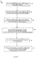
- FIGS. 4A and 4B illustrate a flowchart 400 that further describes the operation of the IF demodulator according to embodiments of the invention.
- FIG. 1A illustrates a conventional television receiver 100 A including an RF tuner 102 , a National Television Standards Committee (NTSC) (or Phase Alternation Line (PAL); or Systeme Electronique Couleur Avec Memoir (SECAM)) surface acoustic wave (SAW) filter 150 , an IF SAW filter 104 , an analog IF demodulator 152 , two analog-to-digital (A/D) converters 108 , 156 , a BTSC Decoder 118 , a Video Decoder (VDEC) 116 , and a digital signal processing core 158 .
- Multiple SAW filters 104 , 150 are needed to pre-process the plurality of signals that exist in today's television signals.
- an NTSC signal requires a NTSC SAW filter 150 to pre-process the NTSC signal, and an analog NTSC IF demodulator 152 .
- a 6 MHz SAW 104 is typically used to pre-process a digital television signal.
- a separate A/D converters are required for each.
- the analog video and digital TV signals can be processed with the same A/D converter. After the signals are digitized, they are decoded by the BTSC decoder 118 for the audio signal and the VDEC 116 for the video signal.
- the digital TV signal is processed in the down stream core 158 .
- the term ‘digital video signal’ refers to a digitized version of an analog video signal.
- FIG. 1B illustrates a television receiver 100 B implementing the present invention.
- Receiver 100 B includes an RF tuner 102 , an IF filter 104 (e.g. SAW filter), and a IF processor/demodulator 117 .
- the IF processor 117 can be configured on a single semiconductor substrate, as indicated by the chip boundary line 124 .
- the tuner 102 receives an RF input signal 101 having a plurality of channels, for example, TV channels that are spaced 6 MHz apart.
- the RF tuner 102 selects and down-converts a desired channel to an IF signal that is output from the tuner 102 .
- the IF signal can be at a frequency of 36 MHz, 44 MHz, or some other IF frequency.
- the SAW filter 104 receives the IF signal from the tuner 104 and filters the IF signal to remove any remaining unwanted channels.
- the tuner 102 can be implemented on a single substrate, as further described in “Digital IF Demodulator For Video Applications”, Application No. 09/739,349, filed on Dec. 15, 2000, which is incorporated herein by reference.
- the IF processor 117 receives the IF signal from the SAW filter 104 , and demodulates the IF signal, to produce a digital video signal 120 and a digital audio signal 122 , that carry for example TV programming or other information.
- the IF processor 117 includes a 2:1 multiplexer, an A/D converter 108 , an IF demodulator 110 , a QAM receiver 112 , a 2:1 multiplexer 114 , a video decoder 116 , and a BTSC decoder 118 .
- the IF processor 117 can be configured on a single substrate, such as for example a CMOS substrate.
- the 2:1 multiplexer 106 in the IF processor 117 multiplexes the IF signal from the SAW filter 106 with any baseband video signal that may be present to produce an analog IF input signal 107 that is sent to the A/D converter 108 .
- the A/D converter 108 digitizes the output of the 2:1 multiplexer 106 .
- the IF demodulator 110 receives the digitized output from the A/D converter 108 , and down-converts the A/D converter 108 output to produce a digital video signal 113 and a digital audio signal 111 .
- the digital audio signal 111 can be a BTSC compatible digital audio signal
- the digital video signal 113 can be a composite video broadcasting signal (CVBS).
- the BTSC decoder 118 receives the digital audio output 111 from the IF demodulator 110 and generates a decoded audio output 122 .
- the 2:1 multiplexer 114 receives the digital video output 113 from the IF demodulator 110 and multiplexes it with the output from the A/D converter 108 .
- a video decoder 116 decodes the output of the 2:1 multiplexer to produce the video signal 120 .
- the IF processor 117 can also include a QAM receiver 112 to process an output of the A/D converter 108 that includes QAM data.
- the IF demodulator 110 and the QAM receiver 112 use common circuit elements.
- IF demodulator 110 processes both an NTSC analog video signal (or a PAL signal or a SECAM signal), along with a digital television signal (e.g., a QAM television signal).
- a digital television signal e.g., a QAM television signal.
- the present invention thus eliminates the need for a separate NTSC SAW filter 150 (FIG. 1A), the NTSC IF demodulator 152 , and the additional A/D converter 156 that are shown in FIG. 1A.
- the signal path before the chip boundary 124 is unified, thus simplifying the tuner output and filtering requirements.
- FIG. 2 further illustrates the IF demodulator 110 that receives the analog IF input signal 107 and generates a digital audio signal 250 and a digital video signal 252 that is ready for baseband decoding by the decoders 116 and 118 .
- the IF demodulator 110 includes a programmable gain amplifier (PGA) 204 , the A/D converter 108 , an AGC 210 , a tuner interface 212 , a first complex mixer 206 , a second complex mixer 208 , lowpass filters 232 and 236 , a nyquist filter 234 , filters 220 and 222 , FM demodulator 224 , a group delay filter 242 , an audio trap 246 , a DC level adjust 248 , a loop filter 238 , and a low pass filter 240 .
- the A/D converter 108 can be implemented internal or external to the IF demodulator 110 .
- the PGA 204 receives the analog IF input signal 107 and variably amplifies the analog input signal 107 according to an automatic gain control (AGC) circuit 210 .
- the A/D converter 108 receives the output of the PGA 204 and digitizes the output of the PGA 204 to generate a digital signal 205 .
- the AGC 210 examines the amplitude of the digital signal 205 to generate a control signal that controls the PGA 204 .
- the PGA 204 , the A/D converter 108 , and the AGC 210 form an AGC loop that is configured to use the full dynamic range of the A/D converter 108 .
- the A/D converter 108 is configured to sample the output of the PGA 204 so as to down-convert the output of the PGA 204 to second, and lower, IF signal.
- the analog IF picture carrier at 45.75 MHz includes a picture carrier that is recovered by the loop filter 238 .
- the A/D converter 108 is configured to sample the output of the PGA 204 to produce a digital output signal 205 , where the picture carrier is down-converted to 8.25 MHz.
- the A/D converter 108 is configured to sub-sample the output of the PGA 204 so as the effect the down-conversion.
- the complex digital mixer 206 mixes the digital signal 205 with the output of a direct digital frequency synthesizer (DDFS) 228 to down-convert the digital signal 205 to baseband to produce an IQ baseband output.
- the direct digital frequency synthesizer 228 provides a quadrature local oscillator output for the complex mixer 206 .
- the complex digital mixer 206 includes a first multiplier 226 and a second multiplier 230 that are driven in quadrature by the output of the DDFS 228 .
- the frequency of the DDFS is selected so that the picture carrier is down-converted to DC.
- the output of the multiplier 226 can be referred to as the in-phase (I) baseband component, and the output of the multiplier 230 can be referred to as the quadrature (Q) baseband component.
- the quadrature component is filtered by a lowpass filter 240 and a loop filter 238 , where the output of the loop filter 238 controls the frequency of the DDFS 228 .
- the complex mixer 206 , the low pass filter 240 , the loop filter 238 , and the DDFS 228 form a carrier recovery loop 239 (similar to a phase lock loop) that recovers the picture carrier.
- the carrier recovery loop 239 including the loop filter 238 are configured so that the picture carrier at the output of the complex mixer 206 is down-converted to 0 Hz, or DC. More specifically, the output of the loop filter 238 can be viewed as an error signal that corrects the frequency of the DDFS 228 so that the picture carrier in the analog signal 107 is down-converted to DC at the output of the complex mixer 206 .
- the lowpass filter 232 filters the in-phase baseband output of the multiplier 226 .
- the lowpass filter 236 filters the quadrature baseband output of the multiplier 230 .
- the lowpass I and Q baseband signals from the filters 232 and 234 are then sent to the Nyquist filter 234 .
- the Nyquist filter 234 combines the I and Q outputs from the filters 232 and 234 and performs Nyquist shaping that was traditionally done by the SAW filter at the IF frequency, to produce a baseband signal 241 .
- the group delay filter 242 provides for group delay compensations of the baseband signal 241 .
- the audio trap filter 246 removes the audio signal from the baseband signal, leaving only a video signal that is gain adjusted by the gain adjust 248 , to produce a digital video signal 252 .
- the order of the group delay filter 242 and the audio trap filter 246 can be swapped.
- the gain adjust 248 adjusts both the gain by scaling the signal by some multiplication factor, and adjusts the DC level by adding a DC value to the signal.
- the digital video signal 252 is compatible with CVBS decoding, which includes luminance and chrominance separation.
- the second complex mixer 208 receives the output of the first complex mixer 206 to perform audio signal recovery.
- the carrier recovery loop 239 is configured so that the picture carrier is down-converted to DC.
- the audio carrier occurs at 4.5 MHz for NTSC. Therefore, the second complex mixer 208 mixes the audio carrier at 4.5 MHz down to 0 Hz or DC.
- the DDFS 216 is configured so that the audio carrier at 4.5 MHz is down-converted to DC.
- the DDFS 216 can be tuned to the 4.5 MHz so that the audio carrier at the output of the first complex mixer 206 is down-converted directly to DC by the multipliers 214 and 218 , producing an I Q baseband signal at the output of the complex mixer 206 .
- the complex mixer 208 generates an IQ baseband signal that is filtered and decimated by the filters 220 and 222 to remove unwanted signals, including the video signal.
- the FM demodulator 224 receives the complex audio baseband signal and demodulates it to produce digital audio output signal 250 that can be BTSC compatible, or can be mono.
- FIG. 3 further illustrates the frequency spectrum of a 6 MHz TV channel 300 .
- the TV channel 300 has a picture carrier 302 at DC (or 0 Hz), and a sound carrier 304 that is offset from the picture carrier 302 by 4.5 MHz. Further details of the TV channel 300 are also included including the picture signal envelope having an upper sideband 306 and a vestigal sideband 308 .
- the I signal 310 , Q signal 312 , and the color carrier 314 are also shown for completeness.
- the audio recovery shown is an open loop system where the DDFS 216 generates a fixed frequency that is near the location of the audio carrier at the output of the first complex mixer.
- a frequency offset between the output of the DDFS 216 and the audio carrier at the output of the first complex mixer shows up as a DC offset at the output of the FM demodulator, which can be removed using a DC compensation block.
- the various filters (e.g. Nyquist filter 234 ) in the digital IF demodulator 110 are digital filters that can be implemented using fixed coefficients or programmable coefficients.
- the filters can be implemented with digital signal processors, which add flexibility to design of the demodulator.
- the digital IF demodulator 110 includes a video recovery circuit and an audio recovery circuit.
- the video recovery circuit includes: the complex mixer 206 , the carrier recovery loop 239 , the lowpass filters 232 , 236 , the Nyquist filter 234 , the group delay filter 242 , the audio trap filter 246 , and the gain/DC adjust 248 , so as to generate the digital video output 252 .
- the audio recovery circuit receives the baseband output of the video recovery circuit (e.g complex mixer 206 output) and recovers the digital audio output using the complex mixer 208 , the filter/decimators 220 , 222 , and the FM demodulator 224 .
- FIG. 4 illustrates a flowchart 400 that further describes the operation of the IF demodulator 110 .
- an analog IF signal is received having a video component and an audio component.
- the analog IF signal can be a TV signal or channel that is down-converted by a TV tuner, such as the tuner 102 .
- An exemplary TV channel is shown in FIG. 3.
- step 404 the analog IF signal is digitized to create a digital IF signal having the video component and the audio component.
- the A/D converter 108 digitizes the analog IF input 107 .
- a first local oscillator signal is generated so that it can be used for down-conversion of the digital IF signal.
- the DDFS 228 generates a quadrature local oscillator signal for the complex mixer 206 .
- the frequency of the first local oscillator is determined so that the picture carrier in the video component of the digital IF signal is down-converted to DC.
- step 408 the digital IF signal is then down-converted to baseband using the first local oscillator signal to generate a baseband signal having a video component and an audio component.
- the complex mixer 206 down-converts the output of the A/D converter 108 using the quadrature local oscillator signal.
- a picture carrier is recovered from the video component of the baseband signal.
- the carrier recovery loop 239 recovers the picture carrier from the baseband output of the complex mixer 206 .
- step 412 the frequency of the first local oscillator signal is adjusted, or tuned, so that the picture carrier is down-converted to DC during step 408 .
- the carrier recovery loop 239 adjusts the frequency of the first local oscillator signal generated by the DDFS 228 so that the picture carrier in the output of the complex mixer 206 is down-converted to DC.
- step 414 the video component of the baseband signal is recovered from the baseband signal generated in step 408 .
- the digital video signal 252 is generated by combining and filtering the baseband output of the complex mixer 206 , including Nyquist filtering by the Nyquist filter 234 .
- a second local oscillator signal is generated having a frequency that is selected so that the audio carrier in the baseband signal is down-converted to approximately DC.
- the second local oscillator signal is relatively fixed compared to the first local oscillator signal since the audio carrier is relatively fixed relative to the picture carrier at DC.
- the DDFS 216 generates a quadrature local oscillator signal having a relatively fixed frequency (e.g. 4.5 MHz) for the complex mixer 208 .
- step 418 the audio component in the baseband signal (of step 408 ) is down-converted using the second local oscillator signal in order to recover the audio component in the baseband signal.
- the complex mixer 206 down-converts the output of the A/D converter 108 using the quadrature local oscillator signal from the DDFS 216 .
- step 420 the audio component is filtered and decimated prior to FM demodulation in step 422 .
- the output of the complex mixer 208 is filtered and FM demodulated to generate the digital audio signal 250 .
Abstract
Description
- This application is a Continuation-In-Part of U.S. Non-Provisional Application entitled “Digital IF Demodulator for Video Applications,” Ser. No. 09/739,349, filed Dec. 15, 2000, which is incorporated by reference herein in its entirety; and this application also claims the benefit of U.S. Provisional Patent Application No. 60/401,043, filed on Aug. 6, 2002, which is incorporated by reference herein in its entirety.
- 1. Field of the Invention
- The present invention is related to a digital IF demodulator, and more specifically to a digital IF demodulator for processing television signals.
- 2. Background Art
- Various analog IF demodulators are used to process television signals.
- These analog approaches require very accurate filter implementations that often require expensive and time consuming tuning of individual units. To properly recover the video, the shape of the Nyquist filter in the receiver needs to be defined accurately, and the tuner needs to accurately center the picture carrier exactly in the middle of the Nyquist slope of the IF filter, which requires high precision phase lock loops in the tuner. Conventionally, this required separate preprocessing filters for NTSC analog television signals and digital television signals, as well as a separate IF demodulator for the NTSC analog signal. Thus, what is needed is a digital IF demodulator that lessens the filtering requirements on the RF tuner.
- It is also desirable to integrate the IF demodulator onto a single low cost silicon substrate fabricated with the low cost Complementary Metal Oxide Semiconductor (CMOS) process. Such integration reduces part count, cost, and size. Complete integration into a single, low cost substrate has been difficult to achieve because the limitations of the designed circuitry often call for external components. Such external circuitry typically requires components having large values of capacitance and inductance that do not facilitate integration into a single substrate.
- Thus, what is needed is a digital IF demodulator that may be completely integrated onto a single silicon substrate. Such a demodulator would minimize or eliminate external circuitry, and allow efficient and economical integration and fabrication on a single silicon substrate.
- The present invention includes a digital IF demodulator that receives and demodulates an analog IF input signal to produce a digital audio signal and a digital video signal. In embodiments, the analog IF input signal is a television signal or channel that has been down-converted from RF. The digital IF demodulator includes an A/D converter, a first digital complex mixer, a second digital complex mixer, and various digital filters. The A/D converter receives the analog input signal and converts it to digital. The first digital complex mixer receives the output of the A/D converter and down-converts the output of the A/D converter to baseband. Additionally, the picture carrier is recovered from the output of the first digital complex mixer, and fed back to a direct digital synthesizer to control the tuning accuracy of the first digital complex mixer. More specifically, a feedback loop is configured so that the picture carrier is down-converted to DC so as to control the tuning accuracy of the first digital complex mixer. The complex output of the first complex mixer is further processed using Nyquist filtering and other filtering to recover the digital video signal. Such filtering may be accomplished using digital signal processing techniques. The digital audio signal is recovered by further processing the output of the first digital complex mixer.
- When the picture carrier is down-converted to DC, the audio signal is offset from DC by approximately 4.5 Mhz (or by some other amount such as 5.5 MHz, 6.0 MHz, or 6.5 MHz depending on the standard used). A second complex mixer down-converts the output of the first digital complex mixer so that the audio signal at 4.5 MHz is down-converted to baseband. After filtering and demodulation, the digital audio signal is recovered.
- The present invention is described with reference to the accompanying drawings. In the drawings, like reference numbers indicate identical or functionally similar elements. Additionally, the left-most digit(s) of a reference number identifies the drawing in which the reference number first appears.
- FIG. 1A illustrates a conventional television receiver having an RF tuner, a National Television Standards Committee (NTSC) Surface Acoustic Wave (SAW) Filter, an IF SAW filter, an analog IF demodulator, two Analog-to-Digital Converters, a BTSC decoder a Video Decoder (VDEC) and a Digital Signal Processing Core.
- FIG. 1B illustrates a television receiver having an RF tuner, IF SAW filter, and a digital IF demodulator.
- FIG. 2 further illustrates the digital IF demodulator according to embodiments of the present invention.
- FIG. 3 illustrates the frequency spectrum of a TV channel with the picture carrier at 0 Hz (DC), and the sound carrier frequency shifted off DC by 4.5 MHz.
- FIGS. 4A and 4B illustrate a
flowchart 400 that further describes the operation of the IF demodulator according to embodiments of the invention. - FIG. 1A illustrates a conventional television receiver 100A including an
RF tuner 102, a National Television Standards Committee (NTSC) (or Phase Alternation Line (PAL); or Systeme Electronique Couleur Avec Memoir (SECAM)) surface acoustic wave (SAW)filter 150, an IFSAW filter 104, ananalog IF demodulator 152, two analog-to-digital (A/D)converters BTSC Decoder 118, a Video Decoder (VDEC) 116, and a digitalsignal processing core 158.Multiple SAW filters NTSC SAW filter 150 to pre-process the NTSC signal, and an analogNTSC IF demodulator 152. A 6 MHz SAW 104 is typically used to pre-process a digital television signal. In order to process both the analog video and analog audio, a separate A/D converters are required for each. The analog video and digital TV signals can be processed with the same A/D converter. After the signals are digitized, they are decoded by theBTSC decoder 118 for the audio signal and the VDEC 116 for the video signal. The digital TV signal is processed in the downstream core 158. Hereinafter, the term ‘digital video signal’ refers to a digitized version of an analog video signal. - FIG. 1B illustrates a
television receiver 100B implementing the present invention.Receiver 100B includes anRF tuner 102, an IF filter 104 (e.g. SAW filter), and a IF processor/demodulator 117. The IFprocessor 117 can be configured on a single semiconductor substrate, as indicated by thechip boundary line 124. Thetuner 102 receives anRF input signal 101 having a plurality of channels, for example, TV channels that are spaced 6 MHz apart. TheRF tuner 102 selects and down-converts a desired channel to an IF signal that is output from thetuner 102. For example, the IF signal can be at a frequency of 36 MHz, 44 MHz, or some other IF frequency. TheSAW filter 104 receives the IF signal from thetuner 104 and filters the IF signal to remove any remaining unwanted channels. Thetuner 102 can be implemented on a single substrate, as further described in “Digital IF Demodulator For Video Applications”, Application No. 09/739,349, filed on Dec. 15, 2000, which is incorporated herein by reference. - The
IF processor 117 receives the IF signal from theSAW filter 104, and demodulates the IF signal, to produce adigital video signal 120 and adigital audio signal 122, that carry for example TV programming or other information. TheIF processor 117 includes a 2:1 multiplexer, an A/D converter 108, an IFdemodulator 110, aQAM receiver 112, a 2:1multiplexer 114, avideo decoder 116, and aBTSC decoder 118. As indicated from thechip boundary 124, theIF processor 117 can be configured on a single substrate, such as for example a CMOS substrate. - The 2:1
multiplexer 106 in theIF processor 117 multiplexes the IF signal from theSAW filter 106 with any baseband video signal that may be present to produce an analog IF input signal 107 that is sent to the A/D converter 108. The A/D converter 108 digitizes the output of the 2:1multiplexer 106. The IF demodulator 110 receives the digitized output from the A/D converter 108, and down-converts the A/D converter 108 output to produce adigital video signal 113 and a digital audio signal 111. The digital audio signal 111 can be a BTSC compatible digital audio signal, and thedigital video signal 113 can be a composite video broadcasting signal (CVBS). TheBTSC decoder 118 receives the digital audio output 111 from theIF demodulator 110 and generates a decodedaudio output 122. The 2:1multiplexer 114 receives thedigital video output 113 from theIF demodulator 110 and multiplexes it with the output from the A/D converter 108. Avideo decoder 116 decodes the output of the 2:1 multiplexer to produce thevideo signal 120. - The
IF processor 117 can also include aQAM receiver 112 to process an output of the A/D converter 108 that includes QAM data. In embodiments, theIF demodulator 110 and theQAM receiver 112 use common circuit elements. - IF
demodulator 110 processes both an NTSC analog video signal (or a PAL signal or a SECAM signal), along with a digital television signal (e.g., a QAM television signal). Such flexibility simplifies the front end receiver requirements by unifying the signal path prior to thedemodulator 110, thus reducing both cost and part count. The present invention thus eliminates the need for a separate NTSC SAW filter 150 (FIG. 1A), the NTSC IFdemodulator 152, and the additional A/D converter 156 that are shown in FIG. 1A. The signal path before thechip boundary 124 is unified, thus simplifying the tuner output and filtering requirements. - FIG. 2 further illustrates the IF demodulator 110 that receives the analog IF input signal 107 and generates a
digital audio signal 250 and adigital video signal 252 that is ready for baseband decoding by thedecoders D converter 108, an AGC 210, a tuner interface 212, a firstcomplex mixer 206, a secondcomplex mixer 208,lowpass filters nyquist filter 234,filters 220 and 222, FM demodulator 224, agroup delay filter 242, anaudio trap 246, a DC level adjust 248, aloop filter 238, and alow pass filter 240. Note that the A/D converter 108 can be implemented internal or external to theIF demodulator 110. - The
PGA 204 receives the analog IF input signal 107 and variably amplifies the analog input signal 107 according to an automatic gain control (AGC) circuit 210. The A/D converter 108 receives the output of thePGA 204 and digitizes the output of thePGA 204 to generate adigital signal 205. The AGC 210 examines the amplitude of thedigital signal 205 to generate a control signal that controls thePGA 204. As such, thePGA 204, the A/D converter 108, and the AGC 210 form an AGC loop that is configured to use the full dynamic range of the A/D converter 108. - The A/
D converter 108 is configured to sample the output of thePGA 204 so as to down-convert the output of thePGA 204 to second, and lower, IF signal. - For example, the analog IF picture carrier at 45.75 MHz includes a picture carrier that is recovered by the
loop filter 238. In one embodiment, the A/D converter 108 is configured to sample the output of thePGA 204 to produce adigital output signal 205, where the picture carrier is down-converted to 8.25 MHz. In one embodiment, the A/D converter 108 is configured to sub-sample the output of thePGA 204 so as the effect the down-conversion. - The complex
digital mixer 206 mixes thedigital signal 205 with the output of a direct digital frequency synthesizer (DDFS) 228 to down-convert thedigital signal 205 to baseband to produce an IQ baseband output. The directdigital frequency synthesizer 228 provides a quadrature local oscillator output for thecomplex mixer 206. The complexdigital mixer 206 includes a first multiplier 226 and asecond multiplier 230 that are driven in quadrature by the output of theDDFS 228. The frequency of the DDFS is selected so that the picture carrier is down-converted to DC. The output of the multiplier 226 can be referred to as the in-phase (I) baseband component, and the output of themultiplier 230 can be referred to as the quadrature (Q) baseband component. The quadrature component is filtered by alowpass filter 240 and aloop filter 238, where the output of theloop filter 238 controls the frequency of theDDFS 228. - The
complex mixer 206, thelow pass filter 240, theloop filter 238, and theDDFS 228 form a carrier recovery loop 239 (similar to a phase lock loop) that recovers the picture carrier. In one embodiment, thecarrier recovery loop 239 including theloop filter 238 are configured so that the picture carrier at the output of thecomplex mixer 206 is down-converted to 0 Hz, or DC. More specifically, the output of theloop filter 238 can be viewed as an error signal that corrects the frequency of theDDFS 228 so that the picture carrier in the analog signal 107 is down-converted to DC at the output of thecomplex mixer 206. - The
lowpass filter 232 filters the in-phase baseband output of the multiplier 226. Likewise, thelowpass filter 236 filters the quadrature baseband output of themultiplier 230. The lowpass I and Q baseband signals from thefilters Nyquist filter 234. TheNyquist filter 234 combines the I and Q outputs from thefilters baseband signal 241. Thegroup delay filter 242 provides for group delay compensations of thebaseband signal 241. Theaudio trap filter 246 removes the audio signal from the baseband signal, leaving only a video signal that is gain adjusted by the gain adjust 248, to produce adigital video signal 252. - The order of the
group delay filter 242 and theaudio trap filter 246 can be swapped. The gain adjust 248 adjusts both the gain by scaling the signal by some multiplication factor, and adjusts the DC level by adding a DC value to the signal. In embodiments, thedigital video signal 252 is compatible with CVBS decoding, which includes luminance and chrominance separation. - The second
complex mixer 208 receives the output of the firstcomplex mixer 206 to perform audio signal recovery. As discussed above, thecarrier recovery loop 239 is configured so that the picture carrier is down-converted to DC. When the picture carrier is at DC, the audio carrier occurs at 4.5 MHz for NTSC. Therefore, the secondcomplex mixer 208 mixes the audio carrier at 4.5 MHz down to 0 Hz or DC. More specifically, theDDFS 216 is configured so that the audio carrier at 4.5 MHz is down-converted to DC. For example, theDDFS 216 can be tuned to the 4.5 MHz so that the audio carrier at the output of the firstcomplex mixer 206 is down-converted directly to DC by themultipliers complex mixer 206. Thecomplex mixer 208 generates an IQ baseband signal that is filtered and decimated by thefilters 220 and 222 to remove unwanted signals, including the video signal. The FM demodulator 224 receives the complex audio baseband signal and demodulates it to produce digitalaudio output signal 250 that can be BTSC compatible, or can be mono. - As discussed above, the audio carrier is offset from the picture carrier by 4.5 MHz for NTSC. Other frequency offsets could be possible depending on the standard used. For example, the audio carrier could be offset by 5.5 MHz, 6.0 MHz, and/or 6.5 MHz, or by some other amount. FIG. 3 further illustrates the frequency spectrum of a 6
MHz TV channel 300. TheTV channel 300 has apicture carrier 302 at DC (or 0 Hz), and asound carrier 304 that is offset from thepicture carrier 302 by 4.5 MHz. Further details of theTV channel 300 are also included including the picture signal envelope having an upper sideband 306 and avestigal sideband 308. The I signal 310, Q signal 312, and thecolor carrier 314 are also shown for completeness. - The audio recovery shown is an open loop system where the
DDFS 216 generates a fixed frequency that is near the location of the audio carrier at the output of the first complex mixer. A frequency offset between the output of theDDFS 216 and the audio carrier at the output of the first complex mixer shows up as a DC offset at the output of the FM demodulator, which can be removed using a DC compensation block. - The various filters (e.g. Nyquist filter 234) in the digital IF
demodulator 110 are digital filters that can be implemented using fixed coefficients or programmable coefficients. For example, the filters can be implemented with digital signal processors, which add flexibility to design of the demodulator. - Based on the discussion above, the digital IF
demodulator 110 includes a video recovery circuit and an audio recovery circuit. The video recovery circuit includes: thecomplex mixer 206, thecarrier recovery loop 239, the lowpass filters 232, 236, theNyquist filter 234, thegroup delay filter 242, theaudio trap filter 246, and the gain/DC adjust 248, so as to generate thedigital video output 252. The audio recovery circuit receives the baseband output of the video recovery circuit (e.gcomplex mixer 206 output) and recovers the digital audio output using thecomplex mixer 208, the filter/decimators 220,222, and theFM demodulator 224. - FIG. 4 illustrates a
flowchart 400 that further describes the operation of theIF demodulator 110. Instep 402, an analog IF signal is received having a video component and an audio component. The analog IF signal can be a TV signal or channel that is down-converted by a TV tuner, such as thetuner 102. An exemplary TV channel is shown in FIG. 3. - In
step 404, the analog IF signal is digitized to create a digital IF signal having the video component and the audio component. For example, the A/D converter 108 digitizes the analog IF input 107. - In
step 406, a first local oscillator signal is generated so that it can be used for down-conversion of the digital IF signal. For example, theDDFS 228 generates a quadrature local oscillator signal for thecomplex mixer 206. As discussed below instep 412, the frequency of the first local oscillator is determined so that the picture carrier in the video component of the digital IF signal is down-converted to DC. - In
step 408, the digital IF signal is then down-converted to baseband using the first local oscillator signal to generate a baseband signal having a video component and an audio component. For example, thecomplex mixer 206 down-converts the output of the A/D converter 108 using the quadrature local oscillator signal. - In
step 410, a picture carrier is recovered from the video component of the baseband signal. For example, thecarrier recovery loop 239 recovers the picture carrier from the baseband output of thecomplex mixer 206. - In
step 412, the frequency of the first local oscillator signal is adjusted, or tuned, so that the picture carrier is down-converted to DC duringstep 408. For example, thecarrier recovery loop 239 adjusts the frequency of the first local oscillator signal generated by theDDFS 228 so that the picture carrier in the output of thecomplex mixer 206 is down-converted to DC. - In step 414, the video component of the baseband signal is recovered from the baseband signal generated in
step 408. For example, thedigital video signal 252 is generated by combining and filtering the baseband output of thecomplex mixer 206, including Nyquist filtering by theNyquist filter 234. - As discussed above, when the picture carrier is down-converted to DC, then the audio carrier is offset from DC by a frequency offset, for example 4.5 MHz. In
step 416, a second local oscillator signal is generated having a frequency that is selected so that the audio carrier in the baseband signal is down-converted to approximately DC. The second local oscillator signal is relatively fixed compared to the first local oscillator signal since the audio carrier is relatively fixed relative to the picture carrier at DC. For example, theDDFS 216 generates a quadrature local oscillator signal having a relatively fixed frequency (e.g. 4.5 MHz) for thecomplex mixer 208. - In
step 418, the audio component in the baseband signal (of step 408) is down-converted using the second local oscillator signal in order to recover the audio component in the baseband signal. For example, thecomplex mixer 206 down-converts the output of the A/D converter 108 using the quadrature local oscillator signal from theDDFS 216. - In step 420, the audio component is filtered and decimated prior to FM demodulation in
step 422. For example, the output of thecomplex mixer 208 is filtered and FM demodulated to generate thedigital audio signal 250. - Example embodiments of the methods, systems, and components of the present invention have been described herein. As noted elsewhere, these example embodiments have been described for illustrative purposes only, and are not limiting. Other embodiments are possible and are covered by the invention. Such other embodiments will be apparent to persons skilled in the relevant art(s) based on the teachings contained herein. Thus, the breadth and scope of the present invention should not be limited by any of the above-described exemplary embodiments, but should be defined only in accordance with the following claims and their equivalents.
Claims (39)
Priority Applications (8)
| Application Number | Priority Date | Filing Date | Title |
|---|---|---|---|
| US10/448,062 US7239357B2 (en) | 2000-12-15 | 2003-05-30 | Digital IF demodulator with carrier recovery |
| US10/776,991 US7352411B2 (en) | 2000-12-15 | 2004-02-12 | Digital IF demodulator |
| US10/791,686 US7489362B2 (en) | 2003-03-04 | 2004-03-03 | Television functionality on a chip |
| EP04005181A EP1501284A3 (en) | 2003-03-04 | 2004-03-04 | Apparatus, system and methods for providing television functionality on a chip |
| US11/197,735 US7477326B2 (en) | 2000-12-15 | 2005-08-02 | HDTV chip with a single IF strip for handling analog and digital reception |
| US12/076,849 US7834937B2 (en) | 2000-12-15 | 2008-03-24 | Digital IF demodulator |
| US12/367,425 US7961255B2 (en) | 2003-03-04 | 2009-02-06 | Television functionality on a chip |
| US13/160,461 US8854545B2 (en) | 2003-03-04 | 2011-06-14 | Television functionality on a chip |
Applications Claiming Priority (3)
| Application Number | Priority Date | Filing Date | Title |
|---|---|---|---|
| US09/739,349 US7106388B2 (en) | 1999-12-15 | 2000-12-15 | Digital IF demodulator for video applications |
| US40104302P | 2002-08-06 | 2002-08-06 | |
| US10/448,062 US7239357B2 (en) | 2000-12-15 | 2003-05-30 | Digital IF demodulator with carrier recovery |
Related Parent Applications (3)
| Application Number | Title | Priority Date | Filing Date |
|---|---|---|---|
| US09/739,349 Continuation-In-Part US7106388B2 (en) | 1999-12-15 | 2000-12-15 | Digital IF demodulator for video applications |
| US10/629,781 Continuation-In-Part US7102689B2 (en) | 2003-03-04 | 2003-07-30 | Systems and methods for decoding teletext messages |
| US10641295 Continuation-In-Part | 2013-08-15 |
Related Child Applications (6)
| Application Number | Title | Priority Date | Filing Date |
|---|---|---|---|
| US10/629,781 Continuation-In-Part US7102689B2 (en) | 2003-03-04 | 2003-07-30 | Systems and methods for decoding teletext messages |
| US10/641,160 Continuation-In-Part US7688387B2 (en) | 2003-03-04 | 2003-08-15 | 2-D combing in a video decoder |
| US10/641,034 Continuation-In-Part US7409339B2 (en) | 2003-03-04 | 2003-08-15 | Methods and systems for sample rate conversion |
| US10/776,991 Continuation-In-Part US7352411B2 (en) | 2000-12-15 | 2004-02-12 | Digital IF demodulator |
| US10/791,686 Continuation-In-Part US7489362B2 (en) | 2003-03-04 | 2004-03-03 | Television functionality on a chip |
| US11/197,735 Continuation-In-Part US7477326B2 (en) | 2000-12-15 | 2005-08-02 | HDTV chip with a single IF strip for handling analog and digital reception |
Publications (2)
| Publication Number | Publication Date |
|---|---|
| US20030197810A1 true US20030197810A1 (en) | 2003-10-23 |
| US7239357B2 US7239357B2 (en) | 2007-07-03 |
Family
ID=33425064
Family Applications (1)
| Application Number | Title | Priority Date | Filing Date |
|---|---|---|---|
| US10/448,062 Expired - Fee Related US7239357B2 (en) | 2000-12-15 | 2003-05-30 | Digital IF demodulator with carrier recovery |
Country Status (1)
| Country | Link |
|---|---|
| US (1) | US7239357B2 (en) |
Cited By (21)
| Publication number | Priority date | Publication date | Assignee | Title |
|---|---|---|---|---|
| US20030132455A1 (en) * | 2001-10-16 | 2003-07-17 | Kimitake Utsunomiya | Methods and apparatus for implementing a receiver on a monolithic integrated circuit |
| US20030202618A1 (en) * | 2002-04-29 | 2003-10-30 | Broadcom Corporation A, California Corporation | Radio receiver having direct DC offset compensation |
| US20030223017A1 (en) * | 2002-05-28 | 2003-12-04 | Kimitake Utsunomiya | Quadratic nyquist slope filter |
| US20040095513A1 (en) * | 2002-06-05 | 2004-05-20 | Takatsugu Kamata | Quadratic video demodulation with baseband nyquist filter |
| US20040109092A1 (en) * | 2001-04-16 | 2004-06-10 | Ivonete Markman | Gain control for a high definition television demodulator |
| US20050036074A1 (en) * | 2003-08-15 | 2005-02-17 | Broadcom Corporation | Method and system for a digital interface for TV stereo audio decoding |
| US20050039218A1 (en) * | 2003-08-14 | 2005-02-17 | Broadcom Corporation | Integrated circuit BTSC encoder |
| US20050143039A1 (en) * | 2002-05-29 | 2005-06-30 | Takatsugu Kamata | Image rejection quadratic filter |
| US20050190013A1 (en) * | 2002-06-05 | 2005-09-01 | Kimitake Utsunomiya | Frequency discrete LC filter bank |
| US20050264376A1 (en) * | 2003-07-18 | 2005-12-01 | Takatsugu Kamata | Methods and apparatus for an improved discrete LC filter |
| EP1635560A2 (en) | 2004-09-13 | 2006-03-15 | ATI Technologies Inc. | World wide analog television signal receiver |
| US20060210088A1 (en) * | 2004-03-19 | 2006-09-21 | Mediatek Inc. | Decording apparatus and decording method for multiple audio standards |
| US20070083279A1 (en) * | 2004-06-17 | 2007-04-12 | Niigata Seimitsu Co., Ltd. | Modulation output device |
| US20070140328A1 (en) * | 2005-12-16 | 2007-06-21 | Takahiro Sato | Complex coefficient transversal filter and complex frequency converter |
| WO2007145645A1 (en) * | 2006-06-13 | 2007-12-21 | Montage Technology Group, Ltd. | On-chip supply regulators |
| CN100454990C (en) * | 2004-04-05 | 2009-01-21 | 联发科技股份有限公司 | Decoder and decoding method for specifications of multiple audio signal |
| US20100009673A1 (en) * | 2002-04-29 | 2010-01-14 | Broadcom Corporation | Method and system for frequency feedback adjustment in digital receivers |
| US7961255B2 (en) | 2003-03-04 | 2011-06-14 | Broadcom Corporation | Television functionality on a chip |
| EP2107804B1 (en) * | 2008-03-31 | 2012-10-31 | Sony Corporation | Analog TV broadcast signal receiving apparatus and analog TV broadcast signal demodulating apparatus |
| TWI495357B (en) * | 2011-07-19 | 2015-08-01 | Mediatek Inc | Audio processing device and audio systems using the same |
| CN111868557A (en) * | 2018-01-17 | 2020-10-30 | 罗伯特·博世有限公司 | Method and device for evaluating ultrasound signals, ultrasound measuring system and operating device |
Families Citing this family (14)
| Publication number | Priority date | Publication date | Assignee | Title |
|---|---|---|---|---|
| US7352411B2 (en) | 2000-12-15 | 2008-04-01 | Broadcom Corporation | Digital IF demodulator |
| US7425995B2 (en) * | 2003-02-28 | 2008-09-16 | Silicon Laboratories, Inc. | Tuner using a direct digital frequency synthesizer, television receiver using such a tuner, and method therefor |
| US7447493B2 (en) * | 2003-02-28 | 2008-11-04 | Silicon Laboratories, Inc. | Tuner suitable for integration and method for tuning a radio frequency signal |
| US7477325B2 (en) * | 2004-03-29 | 2009-01-13 | Ati Technologies, Inc. | Audio/video separator |
| US7599010B2 (en) * | 2004-05-06 | 2009-10-06 | Realtek Semiconductor Corp. | TV receiver and analog TV signal processing method |
| US7406137B2 (en) * | 2004-08-02 | 2008-07-29 | Realtek Semiconductor Corp. | Carrier recovery system and method thereof |
| US8160526B2 (en) * | 2004-08-13 | 2012-04-17 | Thomson Licensing | Filter configuration for a receiver of multiple broadcast standard signals |
| US20060090179A1 (en) * | 2004-10-26 | 2006-04-27 | Ya-Ling Hsu | System and method for embedding supplemental information into a digital stream of a work of content |
| US7446631B2 (en) * | 2005-03-11 | 2008-11-04 | Rf Stream Corporation | Radio frequency inductive-capacitive filter circuit topology |
| US20060217095A1 (en) * | 2005-03-11 | 2006-09-28 | Takatsuga Kamata | Wideband tuning circuit |
| US8477248B2 (en) * | 2007-07-09 | 2013-07-02 | Sigmatel, Inc. | System and method of demodulating audio signals |
| US9282274B2 (en) * | 2009-06-22 | 2016-03-08 | Entropic Communications, Llc | System and method for reducing intra-channel interference |
| WO2011063361A1 (en) * | 2009-11-20 | 2011-05-26 | Maxlinear, Inc. | Integrated if saw filter in baseband digital design for analog tv (or hybrid) tuner |
| US9160390B2 (en) * | 2011-10-07 | 2015-10-13 | Maxlinear, Inc. | Method and system for impairment shifting |
Citations (9)
| Publication number | Priority date | Publication date | Assignee | Title |
|---|---|---|---|---|
| US5031233A (en) * | 1989-07-11 | 1991-07-09 | At&E Corporation | Single chip radio receiver with one off-chip filter |
| US5715012A (en) * | 1996-03-13 | 1998-02-03 | Samsung Electronics Co., Ltd. | Radio receivers for receiving both VSB and QAM digital HDTV signals |
| US5737035A (en) * | 1995-04-21 | 1998-04-07 | Microtune, Inc. | Highly integrated television tuner on a single microcircuit |
| US6005640A (en) * | 1996-09-27 | 1999-12-21 | Sarnoff Corporation | Multiple modulation format television signal receiver system |
| US6147713A (en) * | 1998-03-09 | 2000-11-14 | General Instrument Corporation | Digital signal processor for multistandard television reception |
| US6233295B1 (en) * | 1998-08-26 | 2001-05-15 | Thomson Licensing S.A. | Segment sync recovery network for an HDTV receiver |
| US6445726B1 (en) * | 1999-04-30 | 2002-09-03 | Texas Instruments Incorporated | Direct conversion radio receiver using combined down-converting and energy spreading mixing signal |
| US6476878B1 (en) * | 1998-10-21 | 2002-11-05 | Scientific-Atlanta, Inc. | Method and apparatus for audio signal processing |
| US6738098B1 (en) * | 1998-09-30 | 2004-05-18 | Thomson Licensing S.A. | Video amplifier with integrated DC level shifting |
-
2003
- 2003-05-30 US US10/448,062 patent/US7239357B2/en not_active Expired - Fee Related
Patent Citations (9)
| Publication number | Priority date | Publication date | Assignee | Title |
|---|---|---|---|---|
| US5031233A (en) * | 1989-07-11 | 1991-07-09 | At&E Corporation | Single chip radio receiver with one off-chip filter |
| US5737035A (en) * | 1995-04-21 | 1998-04-07 | Microtune, Inc. | Highly integrated television tuner on a single microcircuit |
| US5715012A (en) * | 1996-03-13 | 1998-02-03 | Samsung Electronics Co., Ltd. | Radio receivers for receiving both VSB and QAM digital HDTV signals |
| US6005640A (en) * | 1996-09-27 | 1999-12-21 | Sarnoff Corporation | Multiple modulation format television signal receiver system |
| US6147713A (en) * | 1998-03-09 | 2000-11-14 | General Instrument Corporation | Digital signal processor for multistandard television reception |
| US6233295B1 (en) * | 1998-08-26 | 2001-05-15 | Thomson Licensing S.A. | Segment sync recovery network for an HDTV receiver |
| US6738098B1 (en) * | 1998-09-30 | 2004-05-18 | Thomson Licensing S.A. | Video amplifier with integrated DC level shifting |
| US6476878B1 (en) * | 1998-10-21 | 2002-11-05 | Scientific-Atlanta, Inc. | Method and apparatus for audio signal processing |
| US6445726B1 (en) * | 1999-04-30 | 2002-09-03 | Texas Instruments Incorporated | Direct conversion radio receiver using combined down-converting and energy spreading mixing signal |
Cited By (37)
| Publication number | Priority date | Publication date | Assignee | Title |
|---|---|---|---|---|
| US20040109092A1 (en) * | 2001-04-16 | 2004-06-10 | Ivonete Markman | Gain control for a high definition television demodulator |
| US7167215B2 (en) * | 2001-04-16 | 2007-01-23 | Thomson Licensing | Gain control for a high definition television demodulator |
| US7327406B2 (en) | 2001-10-16 | 2008-02-05 | Rfstream Corporation | Methods and apparatus for implementing a receiver on a monolithic integrated circuit |
| US20030132455A1 (en) * | 2001-10-16 | 2003-07-17 | Kimitake Utsunomiya | Methods and apparatus for implementing a receiver on a monolithic integrated circuit |
| US20100009673A1 (en) * | 2002-04-29 | 2010-01-14 | Broadcom Corporation | Method and system for frequency feedback adjustment in digital receivers |
| US8050647B2 (en) * | 2002-04-29 | 2011-11-01 | Broadcom Corporation | Method and system for frequency feedback adjustment in digital receivers |
| US7079595B2 (en) * | 2002-04-29 | 2006-07-18 | Broadcom Corporation | Radio receiver having direct DC offset compensation |
| US20030202618A1 (en) * | 2002-04-29 | 2003-10-30 | Broadcom Corporation A, California Corporation | Radio receiver having direct DC offset compensation |
| US7199844B2 (en) * | 2002-05-28 | 2007-04-03 | Rfstream Corporation | Quadratic nyquist slope filter |
| US20030223017A1 (en) * | 2002-05-28 | 2003-12-04 | Kimitake Utsunomiya | Quadratic nyquist slope filter |
| US20050143039A1 (en) * | 2002-05-29 | 2005-06-30 | Takatsugu Kamata | Image rejection quadratic filter |
| US7116961B2 (en) | 2002-05-29 | 2006-10-03 | Rfstream Corporation | Image rejection quadratic filter |
| US20050190013A1 (en) * | 2002-06-05 | 2005-09-01 | Kimitake Utsunomiya | Frequency discrete LC filter bank |
| US20040095513A1 (en) * | 2002-06-05 | 2004-05-20 | Takatsugu Kamata | Quadratic video demodulation with baseband nyquist filter |
| US7102465B2 (en) | 2002-06-05 | 2006-09-05 | Rfstream Corporation | Frequency discrete LC filter bank |
| US8854545B2 (en) | 2003-03-04 | 2014-10-07 | Broadcom Corporation | Television functionality on a chip |
| US7961255B2 (en) | 2003-03-04 | 2011-06-14 | Broadcom Corporation | Television functionality on a chip |
| US20050264376A1 (en) * | 2003-07-18 | 2005-12-01 | Takatsugu Kamata | Methods and apparatus for an improved discrete LC filter |
| US7183880B2 (en) | 2003-07-18 | 2007-02-27 | Rfstream Corporation | Discrete inductor bank and LC filter |
| US7088202B2 (en) | 2003-07-18 | 2006-08-08 | Rfstream Corporation | Methods and apparatus for an improved discrete LC filter |
| US20050039218A1 (en) * | 2003-08-14 | 2005-02-17 | Broadcom Corporation | Integrated circuit BTSC encoder |
| US7557862B2 (en) * | 2003-08-14 | 2009-07-07 | Broadcom Corporation | Integrated circuit BTSC encoder |
| US20050036074A1 (en) * | 2003-08-15 | 2005-02-17 | Broadcom Corporation | Method and system for a digital interface for TV stereo audio decoding |
| US20060210088A1 (en) * | 2004-03-19 | 2006-09-21 | Mediatek Inc. | Decording apparatus and decording method for multiple audio standards |
| US7853021B2 (en) | 2004-03-19 | 2010-12-14 | Mediatek Inc. | Decoding apparatus and decoding method for multiple audio standards |
| CN100454990C (en) * | 2004-04-05 | 2009-01-21 | 联发科技股份有限公司 | Decoder and decoding method for specifications of multiple audio signal |
| US20070083279A1 (en) * | 2004-06-17 | 2007-04-12 | Niigata Seimitsu Co., Ltd. | Modulation output device |
| US7496419B2 (en) * | 2004-06-17 | 2009-02-24 | Niigata Seimitsu Co., Ltd. | Modulation output device |
| EP1635560A3 (en) * | 2004-09-13 | 2007-11-21 | ATI Technologies Inc. | World wide analog television signal receiver |
| EP1635560A2 (en) | 2004-09-13 | 2006-03-15 | ATI Technologies Inc. | World wide analog television signal receiver |
| US7912152B2 (en) * | 2005-12-16 | 2011-03-22 | Samsung Electronics Co., Ltd. | Complex coefficient transversal filter and complex frequency converter |
| US20070140328A1 (en) * | 2005-12-16 | 2007-06-21 | Takahiro Sato | Complex coefficient transversal filter and complex frequency converter |
| US7366926B2 (en) | 2006-06-13 | 2008-04-29 | Montage Technology Group Limited | On-chip supply regulators |
| WO2007145645A1 (en) * | 2006-06-13 | 2007-12-21 | Montage Technology Group, Ltd. | On-chip supply regulators |
| EP2107804B1 (en) * | 2008-03-31 | 2012-10-31 | Sony Corporation | Analog TV broadcast signal receiving apparatus and analog TV broadcast signal demodulating apparatus |
| TWI495357B (en) * | 2011-07-19 | 2015-08-01 | Mediatek Inc | Audio processing device and audio systems using the same |
| CN111868557A (en) * | 2018-01-17 | 2020-10-30 | 罗伯特·博世有限公司 | Method and device for evaluating ultrasound signals, ultrasound measuring system and operating device |
Also Published As
| Publication number | Publication date |
|---|---|
| US7239357B2 (en) | 2007-07-03 |
Similar Documents
| Publication | Publication Date | Title |
|---|---|---|
| US7239357B2 (en) | Digital IF demodulator with carrier recovery | |
| US7834937B2 (en) | Digital IF demodulator | |
| AU747600B2 (en) | Digital signal processor for multistandard television reception | |
| US7075585B2 (en) | Broadband receiver having a multistandard channel filter | |
| US7265792B2 (en) | Television receiver for digital and analog television signals | |
| EP1635560A2 (en) | World wide analog television signal receiver | |
| US20080062334A1 (en) | Apparatus and Method for Restoring DC Spectrum for Analog Television Reception Using Direct Conversion Tuners | |
| US9077936B2 (en) | Integrated IF SAW filter in baseband digital design for analog TV (or hybrid) tuner | |
| US8264617B2 (en) | Analog TV broadcast signal receiving apparatus and analog TV broadcast signal demodulating apparatus | |
| EP1747668B1 (en) | Apparatus and method for processing a pilot signal | |
| EP1706994A1 (en) | Broadband receiver having a multistandard channel filter | |
| US7570110B2 (en) | Arrangement for demodulating a vestigal sideband signal | |
| EP1395048A1 (en) | Analog television signal receiving method and device | |
| JP2005535161A (en) | Secondary video demodulation by baseband Nyquist filter | |
| KR100195710B1 (en) | A demodlation for vsb, qam and ntsc signals | |
| KR0124595B1 (en) | Recover apparatus of digital carrier in hdtv | |
| Yanqing et al. | A design of front-end compatible with PAL & DVB-C | |
| MXPA00008840A (en) | Digital signal processor for multistandard television reception | |
| WO2009118669A2 (en) | Method and apparatus for processing an analog intermediate frequency television signal | |
| JP2003250099A (en) | Receiver | |
| JPH09149410A (en) | Base band signal processing circuit for satellite broadcasting receiving and satellite broadcasting receiver |
Legal Events
| Date | Code | Title | Description |
|---|---|---|---|
| AS | Assignment |
Owner name: BROADCOM CORPORATION, CALIFORNIA Free format text: ASSIGNMENT OF ASSIGNORS INTEREST;ASSIGNOR:JAFFE, STEVEN T.;REEL/FRAME:014129/0677 Effective date: 20030527 |
|
| FPAY | Fee payment |
Year of fee payment: 4 |
|
| REMI | Maintenance fee reminder mailed | ||
| LAPS | Lapse for failure to pay maintenance fees | ||
| STCH | Information on status: patent discontinuation |
Free format text: PATENT EXPIRED DUE TO NONPAYMENT OF MAINTENANCE FEES UNDER 37 CFR 1.362 |
|
| FP | Lapsed due to failure to pay maintenance fee |
Effective date: 20150703 |
|
| AS | Assignment |
Owner name: BANK OF AMERICA, N.A., AS COLLATERAL AGENT, NORTH CAROLINA Free format text: PATENT SECURITY AGREEMENT;ASSIGNOR:BROADCOM CORPORATION;REEL/FRAME:037806/0001 Effective date: 20160201 Owner name: BANK OF AMERICA, N.A., AS COLLATERAL AGENT, NORTH Free format text: PATENT SECURITY AGREEMENT;ASSIGNOR:BROADCOM CORPORATION;REEL/FRAME:037806/0001 Effective date: 20160201 |
|
| AS | Assignment |
Owner name: AVAGO TECHNOLOGIES GENERAL IP (SINGAPORE) PTE. LTD., SINGAPORE Free format text: ASSIGNMENT OF ASSIGNORS INTEREST;ASSIGNOR:BROADCOM CORPORATION;REEL/FRAME:041706/0001 Effective date: 20170120 Owner name: AVAGO TECHNOLOGIES GENERAL IP (SINGAPORE) PTE. LTD Free format text: ASSIGNMENT OF ASSIGNORS INTEREST;ASSIGNOR:BROADCOM CORPORATION;REEL/FRAME:041706/0001 Effective date: 20170120 |
|
| AS | Assignment |
Owner name: BROADCOM CORPORATION, CALIFORNIA Free format text: TERMINATION AND RELEASE OF SECURITY INTEREST IN PATENTS;ASSIGNOR:BANK OF AMERICA, N.A., AS COLLATERAL AGENT;REEL/FRAME:041712/0001 Effective date: 20170119 |