US20030207679A1 - Integrated low power channel select filter having high dynamic range and bandwidth - Google Patents
Integrated low power channel select filter having high dynamic range and bandwidth Download PDFInfo
- Publication number
- US20030207679A1 US20030207679A1 US10/138,848 US13884802A US2003207679A1 US 20030207679 A1 US20030207679 A1 US 20030207679A1 US 13884802 A US13884802 A US 13884802A US 2003207679 A1 US2003207679 A1 US 2003207679A1
- Authority
- US
- United States
- Prior art keywords
- filter
- capacitor
- transconductor
- biquad
- replica
- Prior art date
- Legal status (The legal status is an assumption and is not a legal conclusion. Google has not performed a legal analysis and makes no representation as to the accuracy of the status listed.)
- Granted
Links
Images


Classifications
-
- H—ELECTRICITY
- H03—ELECTRONIC CIRCUITRY
- H03H—IMPEDANCE NETWORKS, e.g. RESONANT CIRCUITS; RESONATORS
- H03H11/00—Networks using active elements
- H03H11/02—Multiple-port networks
- H03H11/04—Frequency selective two-port networks
- H03H11/0422—Frequency selective two-port networks using transconductance amplifiers, e.g. gmC filters
- H03H11/0472—Current or voltage controlled filters
-
- H—ELECTRICITY
- H03—ELECTRONIC CIRCUITRY
- H03H—IMPEDANCE NETWORKS, e.g. RESONANT CIRCUITS; RESONATORS
- H03H11/00—Networks using active elements
- H03H11/02—Multiple-port networks
- H03H11/04—Frequency selective two-port networks
- H03H11/0422—Frequency selective two-port networks using transconductance amplifiers, e.g. gmC filters
- H03H11/0433—Two integrator loop filters
-
- H—ELECTRICITY
- H03—ELECTRONIC CIRCUITRY
- H03H—IMPEDANCE NETWORKS, e.g. RESONANT CIRCUITS; RESONATORS
- H03H11/00—Networks using active elements
- H03H11/02—Multiple-port networks
- H03H11/04—Frequency selective two-port networks
- H03H11/0422—Frequency selective two-port networks using transconductance amplifiers, e.g. gmC filters
- H03H11/0461—Current mode filters
-
- H—ELECTRICITY
- H03—ELECTRONIC CIRCUITRY
- H03H—IMPEDANCE NETWORKS, e.g. RESONANT CIRCUITS; RESONATORS
- H03H11/00—Networks using active elements
- H03H11/02—Multiple-port networks
- H03H11/04—Frequency selective two-port networks
- H03H2011/0483—Frequency selective two-port networks using operational transresistance amplifiers [OTRA]
-
- H—ELECTRICITY
- H03—ELECTRONIC CIRCUITRY
- H03H—IMPEDANCE NETWORKS, e.g. RESONANT CIRCUITS; RESONATORS
- H03H2210/00—Indexing scheme relating to details of tunable filters
- H03H2210/01—Tuned parameter of filter characteristics
- H03H2210/012—Centre frequency; Cut-off frequency
-
- H—ELECTRICITY
- H03—ELECTRONIC CIRCUITRY
- H03H—IMPEDANCE NETWORKS, e.g. RESONANT CIRCUITS; RESONATORS
- H03H2210/00—Indexing scheme relating to details of tunable filters
- H03H2210/02—Variable filter component
- H03H2210/021—Amplifier, e.g. transconductance amplifier
-
- H—ELECTRICITY
- H03—ELECTRONIC CIRCUITRY
- H03H—IMPEDANCE NETWORKS, e.g. RESONANT CIRCUITS; RESONATORS
- H03H2210/00—Indexing scheme relating to details of tunable filters
- H03H2210/02—Variable filter component
- H03H2210/025—Capacitor
-
- H—ELECTRICITY
- H03—ELECTRONIC CIRCUITRY
- H03H—IMPEDANCE NETWORKS, e.g. RESONANT CIRCUITS; RESONATORS
- H03H2210/00—Indexing scheme relating to details of tunable filters
- H03H2210/02—Variable filter component
- H03H2210/028—Resistor
-
- H—ELECTRICITY
- H03—ELECTRONIC CIRCUITRY
- H03H—IMPEDANCE NETWORKS, e.g. RESONANT CIRCUITS; RESONATORS
- H03H2210/00—Indexing scheme relating to details of tunable filters
- H03H2210/03—Type of tuning
- H03H2210/036—Stepwise
Definitions
- the present invention relates generally to the field of electronic circuits, and more particularly to a programmable channel select filter having high dynamic range and bandwidth.
- CMOS process technology Due to its compatibility with high levels of integration, CMOS process technology has proven to be a viable candidate for a low-cost radio solution.
- the choice of a radio architecture is of critical importance in achieving a low-power, low-cost design.
- Radio architectures that require no external filtering at IF emerge as the most likely choice for simultaneously meeting the constraints of power and cost. Because there is no filtering prior to the baseband portion of such a receiver, all contiguous channels get downconverted to baseband. For this reason, the baseband channel select filter must be able to handle a large dynamic range (i.e., 60 dB at the input to the filter to pass all IEEE 802.11a blocker specifications) at bandwidths on the order of 10 MHz. In an integrated implementation, the filter frequency response must be stable with respect to variations in temperature and the manufacturing process, an additional constraint which, when combined with the dynamic range and bandwidth requirements, makes the baseband channel select filter one of the most challenging blocks in the design of an integrated direct conversion receiver.
- the present invention is an integrated channel select filter, having high dynamic range and bandwidth, particularly suited for modem wireless device applications such as IEEE 802.11a/b/g, and other similar wireless protocols.
- the present invention provides a filter comprising at least one transconductor-capacitor (gm-C) filter having an adjustable capacitance, a replica transconductor-capacitor (gm-C) filter having an adjustable capacitance similar to the at least one transconductor-capacitor (gm-C) filter, a clock device coupled to an input of the replica transconductor-capacitor (gm-C) filter, a phase detector coupled to an output of the replica transconductor-capacitor (gm-C) filter and configured to detect a phase shift in an output signal of the replica transconductor-capacitor (gm-C) filter, wherein an amount of phase shift detected by the phase detector is utilized to adjust the capacitance in the at least one transconductor-
- the present invention may further include a transresistance amplifier having an adjustable resistance, connected to an output of at least one transconductor-capacitor (gm-C) filter.
- the operation of the filter circuit may be controlled by a state machine, connected to output a control signal to the at least one transconductor-capacitor (gm-C) filter and the replica transconductor-capacitor (gm-C) filter, in order to adjust the adjustable capacitance.
- the present invention may include at least one transconductor-capacitor (gm-C) filter having an adjustable capacitance and a programmable gain, a replica transconductor-capacitor (gm-C) filter having an adjustable capacitance similar to the at least one transconductor-capacitor (gm-C) filter, a transresistance amplifier, having an adjustable resistance, connected to an output of the at least one transconductor-capacitor (gm-C) filter, a clock device coupled to an input of the replica transconductor-capacitor (gm-C) filter, and a phase detector coupled to an output of the replica transconductor-capacitor (gm-C) filter and configured to detect a phase shift in a signal output by the replica transconductor-capacitor (gm-C) filter.
- gm-C transconductor-capacitor
- An amount of phase shift detected by the phase detector is utilized to adjust the capacitance in the at least one transconductor-capacitor (gm-C) filter and the replica transconductor-capacitor (gm-C) filter, in order to tune a cut-off frequency of the filter circuit. Additionally, a gain is set by adjusting the programmable gain the at least one transconductor-capacitor (gm-C) filter and the adjustable resistance in the transresistance amplifier.
- the present invention includes a method of filtering an input signal, the method comprising filtering the input signal with at least one transconductor-capacitor (gm-C) filter, wherein the operation of the at least one transconductor-capacitor (gm-C) is automatically controlled.
- gm-C transconductor-capacitor
- the method of automatic control comprises inputting a clock signal into a replica transconductor-capacitor (gm-C) filter, detecting a phase shift in an output signal of the replica transconductor-capacitor (gm-C) filter, and adjusting a capacitance in the at least one transconductor-capacitor (gm-C) and the replica transconductor-capacitor (gm-C) filter, based upon the detected phase shift.
- the method may further include amplifying the output signal of the at least one transconductor-capacitor (gm-C) filter with a transresistance amplifier.
- the present invention includes a method of filtering an input signal, the method comprising filtering the input signal with a low Q biquad filter, filtering an output of the low Q biquad with a high Q biquad filter, and amplifying an output of the high Q biquad filter with a transresistance amplifier.
- the biquad filters are adjusted to automatically tune a cut-off frequency of the filter.
- the method of adjusting comprises inputting a clock signal into a replica biquad filter, detecting a phase shift in an output signal of the replica biquad filter, and adjusting a capacitance in the low Q biquad filter, the high Q biquad filter and the replica biquad filter, based upon the detected phase shift.
- FIG. 1 is a block diagram of a channel select filter according to an embodiment of the present invention
- FIG. 2 is a circuit diagram of a digitally controlled capacitor array according to an embodiment of the present invention.
- FIG. 3 is a circuit diagram of a transresistance amplifier with a digitally controlled resistor network according to an embodiment of the present invention
- FIG. 4A is a circuit diagram of a gm-C biquad topology according to an embodiment of the present invention.
- FIG. 4B is a circuit diagram of an alternate gm-C biquad topology according to an embodiment of the present invention.
- FIG. 5 is a circuit diagram of a transistor based fixed-gm transconductor according to an embodiment of the present invention.
- FIG. 6 is a circuit diagram of a transistor based programmable-gm transconductor unit cell according to an embodiment of the present invention.
- FIG. 7A is a block circuit diagram of a replica tuning circuit according to an embodiment of the present invention.
- FIG. 7B is a timing diagram of the replica tuning circuit illustrated in FIG. 7A.
- FIG. 8 is a state diagram of a capacitor selection state machine according to an embodiment of the present invention.
- the present invention is an integrated channel select filter, having high dynamic range and bandwidth, particularly suited for modern wireless device applications such as IEEE 802.11a/b/g, and other similar wireless protocols.
- the present invention is especially suited to operate in a “turbo mode” system, in which data is transmitted at twice the speed of the normal 802.11a transmission.
- a protocol having eight contiguous channels, which are each intended to be used by separate users.
- turbo mode two of the channels are utilized to communicate with a single user, thereby doubling the data rate.
- implementing a turbo mode under 802.11a protocol would increase the data rates from a standard 54 Mbits/sec to 108 Mbits/sec.
- the baseband bandwidth of such a turbo mode system is 17.5 MHz.
- the present invention utilizes a current-mode transconductor-capacitor (gm-C) architecture, tuned by means of digitally-controlled capacitor arrays.
- gm-C current-mode transconductor-capacitor
- FIG. 1 a block diagram of a channel select filter 100 according to an embodiment of the present invention is illustrated.
- the present invention is illustrated with two biquad filters in the main signal path, and a replica biquad filter.
- the present invention may be implemented utilizing one or more transconductor-capacitor (gm-C) filters, of which biquad filters are a subset, in the main signal path, and a transconductor-capacitor (gm-C) filter in the replica filter path, without departing from the scope of the present invention.
- the present invention preferably incorporates a transresistance amplifier, but the teachings of the present invention are not limited to circuit configurations having a transresistance amplifier in the signal path.
- the filter 100 includes a three stage circuit arrangement comprising a low Q biquad filter 102 , a high Q biquad filter 104 , and a transresistance amplifier 106 .
- a “biquad filter” is an electronic circuit that realizes a biqradratic transfer function, as is known in the art.
- the low Q biquad 102 takes an input signal 101 and feeds the high Q biquad 104 , which in turn feeds the transresistance amplifier 106 . This provides a filtered output signal 107 .
- the low Q and high Q biquads each take a current signal in, and output a current signal.
- the transresistance amplifier 106 takes in a current and outputs a voltage signal 107 .
- Each of the biquads 102 , 104 are digitally tuned.
- a separate replica biquad tuning circuit (control circuit), includes a clock signal 108 , a replica biquad 110 , a phase detector 120 , and a state machine 130 .
- the tuning circuit provides a binary value 132 that tunes each of the biquads 102 , 104 , 110 in order to implement a desired cut-off frequency of the filter 100 .
- the state machine 130 provides a digital signal 132 that selects a capacitor setting of a capacitor array in the biquads, which tunes the filter accordingly.
- the digital signal 132 from the state machine is based upon the output of the replica biquad 110 and phase detector 120 .
- the replica biquad 100 is a scaled down version of the high Q biquad 104 .
- the replica biquad 110 is tuned to have a ⁇ 3 dB cut-off frequency of 8 MHz.
- One of the characteristics of a biquad circuit is that when it is driven at its cut off frequency, it has exactly 90 degrees of phase shift between its input and its output. Thus, if the phase shift of the replica biquad 110 is detected, and forced to be 90° by using a feedback control scheme, the biquad filter will be at its cut-off frequency.
- the phase detector 120 detects the 90° phase shift, or any variance from the 90° phase shift, and provides the result to the state machine 130 .
- the state machine 130 then drives the other stages ( 102 and 104 ) along with the replica biquad 110 , until the phase shift is exactly 90°.
- an 8 MHz signal 108 is fed into the replica biquad 110 .
- the initial cut-off frequency will generally not be correct (i.e. the phase shift is either too high or too low).
- the phase detector 120 detects the non-90° condition, and outputs a correction signal to the state machine 130 .
- the state machine 130 updates the settings in the replica biquad 110 in order to obtain the preset cut-off frequency.
- the state machine 130 inputs the same information that tuned the replica biquad into the main filter stages ( 102 and 104 ).
- this process automatically sets the cut-off frequency of the main filter, based upon the operating condition of the replica biquad 110 .
- FIG. 2 is a circuit diagram of a digitally controlled capacitor array 200 according to an embodiment of the present invention.
- the capacitor array 200 is fitted at the nodes of each of the low and high Q biquads 102 , 104 and at the replica biquad 110 .
- the capacitor array 200 is used to tune each of the biquads in parallel using the same digital input values.
- the capacitor array 200 includes a series of capacitive cells between the out+ and out ⁇ terminals of the capacitor array 200 .
- Each unit cell 230 has an amount of capacitance that is applied between the out+ and out ⁇ terminals based on a digital input.
- Each cell has one or more switches that connect the cell capacitance between the out+ and out ⁇ terminals.
- cell b 0 , 230 has a capacitance C 0 that is applied between out+ and out ⁇ when a voltage is applied to terminal b 0 .
- the next cell has a 2C 0 capacitance value that is applied between out+ and out ⁇ when a voltage is applied to terminal b 1 .
- Each cell has twice the capacitance of a previous cell, resulting in a series of digital inputs that define an amount of capacitance that is then applied to the biquad filters. Note that all the circuits described herein are fully differential, and thus the capacitor array 200 is illustrated as a differential array.
- the filter transfer function of the channel select filter 100 is a fourth-order Butterworth lowpass, with a ⁇ 3 dB cut-off frequency which is selectable to either 11 MHz (in standard mode) or 22 MHz (in turbo mode).
- the four filter poles are constructed by cascading two biquad (two-pole) filter sections. Each biquad section contains 18 dB of programmable gain in 6 dB steps which, when combined with a third current-to-voltage conversion stage 106 having 5 dB of programmable gain in 1 dB steps, results in 41 dB of total baseband programmable gain range in 1 dB steps.
- the units of the transresistance amplifier gain is in units of Ohms, rather than dB, because the gain is actually the value of the feedback resistor.
- the value of the resistor is converted to dB using the 20 log function used for converting to dB.
- the programmable gain in the biquad stages is implemented through digitally switched current mirrors (FIG. 6), whereas the current-to-voltage stage consists of an op amp transresistance stage with a digitally-controlled resistor network, of which a single-ended version is shown in FIG. 3.
- FIG. 3 is a circuit diagram of a transresistance amplifier 106 with a digitally controlled resistor network according to an embodiment of the present invention.
- An operational amplifier (op-amp) 310 has a series of feedback resistors R 1 . . . R 6 . Each resistor has a corresponding switch that is set by application of a voltage to a corresponding terminal (b 0 . . . b5). Thus, different sets of resistors can be shorted-out to change the properties of the transresistance amplifier 106 . With proper sizing of the resistors, the gain can be adjusted in 1 dB increments.
- FIG. 4A is a circuit diagram of a first gm-C biquad topology according to an embodiment of the present invention.
- FIG. 4B is a circuit diagram of a second gm-C biquad topology according to an alternative embodiment of the present invention. Functionally, the two circuits are equivalent.
- a set of gm stages (gm 1 , gm 2 , gm 3 , and gm 4 ), are shown as trapezoidal blocks. Each gm stage is a circuit block which has an input voltage applied to the longer side of the trapezoid, and a current output on the shorter side.
- a voltage is applied to the left side of the block and a current is output on the right side of the block.
- the output of the block is equal to the gain coefficient of the gm stage (gm 1 ), multiplied by the input voltage or:
- Iout 1 gm 1 ⁇ Vgm 1
- the next stage, gm 3 is negative (i.e. ⁇ gm 3 ) and also the input and output terminals of the block are effectively directly connected. If the voltage is increased (on the left side), the current is pulled down, thus acting like a resistor. The difference is that the effective resistance would be the inverse of gm because gm is in units inverse to resistance (i.e. 1/ ⁇ ).
- Each of the biquad implementations illustrated in FIG. 4 has four gm blocks and two capacitors (C 1 and C 2 ).
- the transfer function of either circuit is shown below. These equations then reduce to specific parts, such as a gain and a cut-off frequency.
- ⁇ c gm 1 ⁇ gm 2 C 1 ⁇ C 2 ( EQ ⁇ ⁇ 3 )
- Q gm 1 ⁇ gm 2 gm 3 ⁇ C 2 C 1 ( EQ ⁇ ⁇ 4 )
- the present implementation adjusts gm 4 since gm 4 is the only parameter which controls gain without affecting either the cutoff frequency or Q. Note that gm 4 is absent in both EQ 3 and EQ 4, above.
- the capacitors C 1 and C 2 are implemented as binary weighted capacitor arrays in parallel, similar to that illustrated in FIG. 2.
- a digital code output by the state machine 130 is sent to terminals b 0 . . . b 4 to set a specific capacitance value.
- the fixed-gm transconductors (gm 1 , gm 2 , gm 3 ) may be implemented as illustrated by the transistor level diagram of FIG. 5.
- the programmable gm-transconductance block (gm 4 ) may be implemented as a parallel connection of eight unit cells, one of which is shown in FIG. 6.
- the gain setting of gm 4 is dictated by how many of the eight unit cells are “on”.
- the four possible settings are 1, 2, 4 or 8, corresponding to 0 dB, 6 dB, 12 dB and 18 dB of gain, relative to the transconductance of a single unit cell. Note that, as illustrated in FIG. 6, when a transconductor unit cell is “off”, the NMOS currents are switched to the positive power supply rail, rather than shut off. Applying the same DC bias in all of the NMOS transistors in each unit cell ensures that the parasitic capacitance contributed by the input of gm 4 remains independent of the gain setting.
- the choice between the two biquad topologies described above is determined by considering signal scaling at the internal node. In order to maximize the dynamic range, the signal power at all four signal nodes of the filter should be kept within reasonable limits.
- the present invention uses the topology of FIG. 4(A) for the first, low Q biquad 102 , and the topology of FIG. 4(B) for the second, high Q biquad 104 . From standard filter theory, in order to achieve a four-pole Butterworth response, the Q of these two biquads is 0.541 and 1.307, respectively.
- One advantage of the present current-mode topology is that linearity is preserved even in the presence of a nonlinear transconductor. Individually, the transconductors do not have particularly linear voltage-to-current characteristics. However, in the context of a current-in/current-out topology, the nonlinearity of the first current-to-voltage conversion is compensated by the non-linearity of the corresponding voltage-to-current conversion. More precisely, the current-mode biquad filter acts like a cascoded current mirror in the passband, and cascoded current mirrors have very good linearity.
- FIG. 7A is a block diagram of a replica biquad tuning circuit according to an embodiment of the present invention.
- the replica tuning circuit includes the replica biquad filter 110 , the phase detector 120 , and the state machine 130 .
- the phase detector 120 is shown in greater detail and includes a pre-amplifier 700 , a comparator 710 , an input capacitor pair C OS , and a pair of phase signals ⁇ 1 and ⁇ 2.
- the pre-amplifier 700 has AC coupling on its input.
- Two switches 701 , 702 are connected across the pre-amplifier 700 , and are controlled by the phase signal ⁇ 1, which is generated by the state machine 130 .
- the polarity of the pre-amplifier 700 is illustrated in FIG. 7(A).
- the negative output is connected to the positive input via one switch 701 , and the positive output is connected to the negative input via the other switch 702 .
- FIG. 7B is a timing diagram of the replica tuning circuit illustrated in FIG. 7A.
- the first signal represents an 8 MHz clock, which is preferably implemented as a square wave with 50% duty cycle, and serves as the input to the replica biquad filter.
- the second signal represents the output of the replica filter when its phase shift is exactly 90 degrees at 8 MHz. Note that the output is not only phase-shifted, but the harmonics of the square wave are filtered as well, resulting in a more sinusoidal waveform.
- the third signal represents the offset sampling phase; specifically, switches 701 and 702 are closed when the ⁇ 1 waveform is high, and open when the ⁇ 1 waveform is low.
- the fourth signal represents the comparator strobe phase; specifically, the comparator is strobed on the rising edge of ⁇ 2.
- the numbers 0 through 7 and labeled ‘count’ refer to the ‘count’ variable in the state diagram (FIG. 8). These count increments are identified in the timing diagram in order to explain the operation of the state diagram in FIG. 8.
- the switched-capacitor pre-amplifier of the phase detector 120 serves two functions: (1) it provides about 12 dB of gain to overcome the DC offset of the comparator; and (2) switched-capacitor operation cancels the DC offset present at the output of the replica biquad, plus a portion of the input-referred offset of the comparator itself. To understand this DC-offset cancellation scheme more clearly, consider the operation of the phase detector when the replica biquad output contains a DC offset.
- V in ⁇ ( replica ) ⁇ cos ⁇ ( 2 ⁇ ⁇ ⁇ ⁇ f ⁇ ⁇ t )
- V ( C OS ) sin( ⁇ )+ V DC (EQ 6)
- the state machine 130 is clocked at 32 MHz, and generates the 8 MHz replica biquad filter input square wave, as well as the clock phases ⁇ 1 (the sample phase) and ⁇ 2 (the compare phase). Note that all of the transitions of the 8 MHz clock and of both the sample and compare phases occur on rising edges of the 32 MHz clock (the first eight of these rising edges are drawn as dotted lines in the figure); this alignment facilitates design of the logic in the state machine, since positive-edge-triggered synchronous logic can generate these three clocks with very good phase accuracy.
- FIG. 8 is a state diagram of a capacitor selection state machine 130 according to an embodiment of the present invention.
- Each state illustrated includes pseudo code, which is an example programming structure for implementing each of the illustrated states.
- the pseudo code for each state is not intended to be a compilable or executable portion of code, but as an example programming structure that provides a non-limiting implementation of a process or method consistent with the present invention.
- the present invention is implemented in a packet based system such as an 802.11a/b/g system. If a system is packet-based, it receives packets periodically, which tend to be on the order of 1 ms long. The receiver is turned on and off with each received packet, and therefore the receiver is turned on with a certain frequency. The present invention tunes the capacitors each time the receiver is turned “on.” Once the filter calibration procedure converges, it holds the correct capacitor settings to tune the filter to the selected cut-off frequency. The held settings are correct, accounting for thermal drift or other variances, for at least one millisecond.
- the filter determines the right settings by determining when there is a transition from a series of “up” requests to a “down” request, or vice versa. That is, if there are a series of up adjustments, and then a down, the filter must be on the transition point between up and down, and it picks the higher state. This type of selection makes the calibration more repeatable. The starting point for the next calibration cycle is just above the same position of the last calibration.
- the calibration can be performed once every millisecond.
- the actual timing of the calibrations may be highly dependent on what kind of traffic the network is experiencing.
- a packet is about 1 ms long and the frequency that the packets are being received is unimportant, since the filter does this calibration at the beginning of each received packet (e.g., each request to receive), and the filter maintains that calibration for the duration of the receive packet.
- the behavior of the state machine can be summarized as follows.
- the state machine begins operation immediately after the receiver is turned on. At this point, the state machine waits a programmable duration period wait_I 810 in order for the power-on transients to settle.
- the state machine enters a loop 820 / 830 in which it performs the offset-sampling and phase comparison operation described with respect to the timing diagram of FIG. 7B.
- the state machine adjusts the capacitor settings, either incrementing the capacitance if the phase is less than 90°, or decrementing it if the phase is greater than 90°.
- the state machine produces a programmable number of comparator strobes (maxstrobes).
- the comparator is oscillating between its two possible states.
- the state machine picks the higher of the two capacitor settings which straddle the transition between up and down, then shuts down the replica filter circuit 840 , and holds the final capacitor setting for the duration of the receive packet 850 .
- the time duration occupied by the capacitor selection is programmable through the parameter maxstrobes. With a careful selection of parameters, the algorithm occupies a maximum of 2 ⁇ sec, and typically takes less than 0.5 ⁇ sec. In either case, the calibration procedure converges to a final capacitance setting before data is expected to be received. Furthermore, since a typical receive packet is on the order of 1 ms long, the average power dissipation of the replica tuning circuit is effectively zero.
- the baseband filter architecture of the present invention contains several innovations over previous implementations.
- the integrated approach possesses four distinct advantages: (1) cost advantages associated with the high level of integration; (2) with careful chip layout, the on-chip components can be expected to match each other better than off-chip components, resulting in better I-Q amplitude and phase matching performance; (3) better cut-off frequency control; and (4) routing signals off-chip is an inconvenience due to increased pin count (for instance, previous passive filter implementations require 12 or more additional I/O pins) and the associated degradation of signal integrity.
- the tuning system chosen for this design possesses several advantages over previous implementations of integrated filters.
- the digital capacitor selection approach does not perturb the signal path; in fact, it does not even dissipate any power.
- the capacitor-tuning approach does not suffer changes in linearity performance across the tuning range.
- the present invention is preferably implemented in a direct conversion receiver, however, the processes and technologies discussed herein may be applied to other receiver types.
- specific terminology is employed for the sake of clarity.
- the present invention is not intended to be limited to the specific terminology so selected, and it is to be understood that each specific element includes all technical equivalents which operate in a similar manner.
- any other equivalent device such as a analog or other variable capacitor, or other device having an equivalent function or capability, whether or not listed herein, may be substituted therewith.
- the inventors recognize that newly developed technologies not now known may also be substituted for the described parts and still not depart from the scope of the present invention. All other described items, including, but not limited to transconductance blocks (gms), op-amps, state machines, clocks, transistors and other electrical components, etc should also be consider in light of any and all available equivalents.
- Portions of the present invention may be conveniently implemented using a conventional general purpose or a specialized digital computer or microprocessor programmed according to the teachings of the present disclosure, as will be apparent to those skilled in the computer art.
Abstract
Description
- 1. Field of the Invention
- The present invention relates generally to the field of electronic circuits, and more particularly to a programmable channel select filter having high dynamic range and bandwidth.
- 2. Description of the Related Art
- With the increased ubiquity of wireless communication devices in offices and homes, one of the most difficult challenges continues to be the design of a cost-effective, power-efficient analog transceiver. Due to its compatibility with high levels of integration, CMOS process technology has proven to be a viable candidate for a low-cost radio solution. The choice of a radio architecture, however, is of critical importance in achieving a low-power, low-cost design.
- Radio architectures that require no external filtering at IF emerge as the most likely choice for simultaneously meeting the constraints of power and cost. Because there is no filtering prior to the baseband portion of such a receiver, all contiguous channels get downconverted to baseband. For this reason, the baseband channel select filter must be able to handle a large dynamic range (i.e., 60 dB at the input to the filter to pass all IEEE 802.11a blocker specifications) at bandwidths on the order of 10 MHz. In an integrated implementation, the filter frequency response must be stable with respect to variations in temperature and the manufacturing process, an additional constraint which, when combined with the dynamic range and bandwidth requirements, makes the baseband channel select filter one of the most challenging blocks in the design of an integrated direct conversion receiver.
- In general, the present invention is an integrated channel select filter, having high dynamic range and bandwidth, particularly suited for modem wireless device applications such as IEEE 802.11a/b/g, and other similar wireless protocols. In one embodiment, the present invention provides a filter comprising at least one transconductor-capacitor (gm-C) filter having an adjustable capacitance, a replica transconductor-capacitor (gm-C) filter having an adjustable capacitance similar to the at least one transconductor-capacitor (gm-C) filter, a clock device coupled to an input of the replica transconductor-capacitor (gm-C) filter, a phase detector coupled to an output of the replica transconductor-capacitor (gm-C) filter and configured to detect a phase shift in an output signal of the replica transconductor-capacitor (gm-C) filter, wherein an amount of phase shift detected by the phase detector is utilized to adjust the capacitance in the at least one transconductor-capacitor (gm-C) filter, and the replica transconductor-capacitor (gm-C) filter, in order to tune a cut-off frequency of the filter circuit.
- The present invention may further include a transresistance amplifier having an adjustable resistance, connected to an output of at least one transconductor-capacitor (gm-C) filter. The operation of the filter circuit may be controlled by a state machine, connected to output a control signal to the at least one transconductor-capacitor (gm-C) filter and the replica transconductor-capacitor (gm-C) filter, in order to adjust the adjustable capacitance.
- In another embodiment, the present invention may include at least one transconductor-capacitor (gm-C) filter having an adjustable capacitance and a programmable gain, a replica transconductor-capacitor (gm-C) filter having an adjustable capacitance similar to the at least one transconductor-capacitor (gm-C) filter, a transresistance amplifier, having an adjustable resistance, connected to an output of the at least one transconductor-capacitor (gm-C) filter, a clock device coupled to an input of the replica transconductor-capacitor (gm-C) filter, and a phase detector coupled to an output of the replica transconductor-capacitor (gm-C) filter and configured to detect a phase shift in a signal output by the replica transconductor-capacitor (gm-C) filter. An amount of phase shift detected by the phase detector is utilized to adjust the capacitance in the at least one transconductor-capacitor (gm-C) filter and the replica transconductor-capacitor (gm-C) filter, in order to tune a cut-off frequency of the filter circuit. Additionally, a gain is set by adjusting the programmable gain the at least one transconductor-capacitor (gm-C) filter and the adjustable resistance in the transresistance amplifier.
- The present invention includes a method of filtering an input signal, the method comprising filtering the input signal with at least one transconductor-capacitor (gm-C) filter, wherein the operation of the at least one transconductor-capacitor (gm-C) is automatically controlled. The method of automatic control comprises inputting a clock signal into a replica transconductor-capacitor (gm-C) filter, detecting a phase shift in an output signal of the replica transconductor-capacitor (gm-C) filter, and adjusting a capacitance in the at least one transconductor-capacitor (gm-C) and the replica transconductor-capacitor (gm-C) filter, based upon the detected phase shift. The method may further include amplifying the output signal of the at least one transconductor-capacitor (gm-C) filter with a transresistance amplifier.
- In one specific embodiment, the present invention includes a method of filtering an input signal, the method comprising filtering the input signal with a low Q biquad filter, filtering an output of the low Q biquad with a high Q biquad filter, and amplifying an output of the high Q biquad filter with a transresistance amplifier. The biquad filters are adjusted to automatically tune a cut-off frequency of the filter. The method of adjusting comprises inputting a clock signal into a replica biquad filter, detecting a phase shift in an output signal of the replica biquad filter, and adjusting a capacitance in the low Q biquad filter, the high Q biquad filter and the replica biquad filter, based upon the detected phase shift.
- The present invention will be readily understood by the following detailed description in conjunction with the accompanying drawings, wherein like reference numerals designate like structural elements, and in which:
- FIG. 1 is a block diagram of a channel select filter according to an embodiment of the present invention;
- FIG. 2 is a circuit diagram of a digitally controlled capacitor array according to an embodiment of the present invention;
- FIG. 3 is a circuit diagram of a transresistance amplifier with a digitally controlled resistor network according to an embodiment of the present invention;
- FIG. 4A is a circuit diagram of a gm-C biquad topology according to an embodiment of the present invention;
- FIG. 4B is a circuit diagram of an alternate gm-C biquad topology according to an embodiment of the present invention;
- FIG. 5 is a circuit diagram of a transistor based fixed-gm transconductor according to an embodiment of the present invention;
- FIG. 6 is a circuit diagram of a transistor based programmable-gm transconductor unit cell according to an embodiment of the present invention;
- FIG. 7A is a block circuit diagram of a replica tuning circuit according to an embodiment of the present invention;
- FIG. 7B is a timing diagram of the replica tuning circuit illustrated in FIG. 7A; and
- FIG. 8 is a state diagram of a capacitor selection state machine according to an embodiment of the present invention.
- The following description is provided to enable any person skilled in the art to make and use the invention and sets forth the best modes contemplated by the inventor for carrying out the invention. Various modifications, however, will remain readily apparent to those skilled in the art. Any and all such modifications, equivalents and alternatives are intended to fall within the spirit and scope of the present invention.
- In general, the present invention is an integrated channel select filter, having high dynamic range and bandwidth, particularly suited for modern wireless device applications such as IEEE 802.11a/b/g, and other similar wireless protocols. The present invention is especially suited to operate in a “turbo mode” system, in which data is transmitted at twice the speed of the normal 802.11a transmission. Consider, for example, a protocol having eight contiguous channels, which are each intended to be used by separate users. In turbo mode, two of the channels are utilized to communicate with a single user, thereby doubling the data rate. Thus, implementing a turbo mode under 802.11a protocol would increase the data rates from a standard 54 Mbits/sec to 108 Mbits/sec. The baseband bandwidth of such a turbo mode system is 17.5 MHz.
- To address the issues of dynamic range and bandwidth in a channel select filter, provide tunability, and other improvements, the present invention utilizes a current-mode transconductor-capacitor (gm-C) architecture, tuned by means of digitally-controlled capacitor arrays. Referring to FIG. 1, a block diagram of a channel
select filter 100 according to an embodiment of the present invention is illustrated. In this particular embodiment, the present invention is illustrated with two biquad filters in the main signal path, and a replica biquad filter. However, the present invention may be implemented utilizing one or more transconductor-capacitor (gm-C) filters, of which biquad filters are a subset, in the main signal path, and a transconductor-capacitor (gm-C) filter in the replica filter path, without departing from the scope of the present invention. Additionally, the present invention preferably incorporates a transresistance amplifier, but the teachings of the present invention are not limited to circuit configurations having a transresistance amplifier in the signal path. - In one particular embodiment, the
filter 100 includes a three stage circuit arrangement comprising a lowQ biquad filter 102, a highQ biquad filter 104, and atransresistance amplifier 106. A “biquad filter” is an electronic circuit that realizes a biqradratic transfer function, as is known in the art. Thelow Q biquad 102 takes aninput signal 101 and feeds thehigh Q biquad 104, which in turn feeds thetransresistance amplifier 106. This provides a filteredoutput signal 107. The low Q and high Q biquads each take a current signal in, and output a current signal. Thetransresistance amplifier 106 takes in a current and outputs avoltage signal 107. Each of thebiquads clock signal 108, areplica biquad 110, aphase detector 120, and astate machine 130. The tuning circuit provides abinary value 132 that tunes each of thebiquads filter 100. More particularly, thestate machine 130 provides adigital signal 132 that selects a capacitor setting of a capacitor array in the biquads, which tunes the filter accordingly. - The
digital signal 132 from the state machine is based upon the output of thereplica biquad 110 andphase detector 120. In order to save power and die area, thereplica biquad 100 is a scaled down version of thehigh Q biquad 104. The replica biquad 110 is tuned to have a −3 dB cut-off frequency of 8 MHz. One of the characteristics of a biquad circuit is that when it is driven at its cut off frequency, it has exactly 90 degrees of phase shift between its input and its output. Thus, if the phase shift of thereplica biquad 110 is detected, and forced to be 90° by using a feedback control scheme, the biquad filter will be at its cut-off frequency. If the same feedback input is used to drive the actual signal path filters (i.e., the high and low Q biquads), then their frequency responses are adjusted in accordance with the adjustment applied to thereplica biquad 110. In further detail, thephase detector 120 detects the 90° phase shift, or any variance from the 90° phase shift, and provides the result to thestate machine 130. Thestate machine 130 then drives the other stages (102 and 104) along with thereplica biquad 110, until the phase shift is exactly 90°. - For example, to obtain a preset cut-off frequency, an 8
MHz signal 108 is fed into thereplica biquad 110. The initial cut-off frequency will generally not be correct (i.e. the phase shift is either too high or too low). Thephase detector 120 detects the non-90° condition, and outputs a correction signal to thestate machine 130. Thestate machine 130 updates the settings in thereplica biquad 110 in order to obtain the preset cut-off frequency. Once the cut-off frequency is established, thestate machine 130 inputs the same information that tuned the replica biquad into the main filter stages (102 and 104). Thus, this process automatically sets the cut-off frequency of the main filter, based upon the operating condition of thereplica biquad 110. - FIG. 2 is a circuit diagram of a digitally controlled capacitor array 200 according to an embodiment of the present invention. The capacitor array 200 is fitted at the nodes of each of the low and high Q biquads 102, 104 and at the
replica biquad 110. The capacitor array 200 is used to tune each of the biquads in parallel using the same digital input values. The capacitor array 200 includes a series of capacitive cells between the out+ and out− terminals of the capacitor array 200. Eachunit cell 230 has an amount of capacitance that is applied between the out+ and out− terminals based on a digital input. Each cell has one or more switches that connect the cell capacitance between the out+ and out− terminals. For example cell b0, 230 has a capacitance C0 that is applied between out+ and out− when a voltage is applied to terminal b0. The next cell has a 2C0 capacitance value that is applied between out+ and out− when a voltage is applied to terminal b1. Each cell has twice the capacitance of a previous cell, resulting in a series of digital inputs that define an amount of capacitance that is then applied to the biquad filters. Note that all the circuits described herein are fully differential, and thus the capacitor array 200 is illustrated as a differential array. - The filter transfer function of the channel
select filter 100 is a fourth-order Butterworth lowpass, with a −3 dB cut-off frequency which is selectable to either 11 MHz (in standard mode) or 22 MHz (in turbo mode). The four filter poles are constructed by cascading two biquad (two-pole) filter sections. Each biquad section contains 18 dB of programmable gain in 6 dB steps which, when combined with a third current-to-voltage conversion stage 106 having 5 dB of programmable gain in 1 dB steps, results in 41 dB of total baseband programmable gain range in 1 dB steps. Specifically, the minimum gain is 1 kΩ (since the input to the filter is a current, and the output a voltage), and the maximum gain is 1 kΩ+41 dB=112.2 kΩ. The units of the transresistance amplifier gain is in units of Ohms, rather than dB, because the gain is actually the value of the feedback resistor. The value of the resistor is converted to dB using the 20 log function used for converting to dB. - The programmable gain in the biquad stages is implemented through digitally switched current mirrors (FIG. 6), whereas the current-to-voltage stage consists of an op amp transresistance stage with a digitally-controlled resistor network, of which a single-ended version is shown in FIG. 3.
- FIG. 3 is a circuit diagram of a
transresistance amplifier 106 with a digitally controlled resistor network according to an embodiment of the present invention. An operational amplifier (op-amp) 310 has a series of feedback resistors R1 . . . R6. Each resistor has a corresponding switch that is set by application of a voltage to a corresponding terminal (b0 . . . b5). Thus, different sets of resistors can be shorted-out to change the properties of thetransresistance amplifier 106. With proper sizing of the resistors, the gain can be adjusted in 1 dB increments. - FIG. 4A is a circuit diagram of a first gm-C biquad topology according to an embodiment of the present invention. FIG. 4B is a circuit diagram of a second gm-C biquad topology according to an alternative embodiment of the present invention. Functionally, the two circuits are equivalent. A set of gm stages (gm 1, gm2, gm3, and gm4), are shown as trapezoidal blocks. Each gm stage is a circuit block which has an input voltage applied to the longer side of the trapezoid, and a current output on the shorter side. For example, on the gm1 block, a voltage is applied to the left side of the block and a current is output on the right side of the block. The output of the block is equal to the gain coefficient of the gm stage (gm1), multiplied by the input voltage or:
- Iout1=gm1×Vgm1
- The next stage, gm 3, is negative (i.e. −gm3) and also the input and output terminals of the block are effectively directly connected. If the voltage is increased (on the left side), the current is pulled down, thus acting like a resistor. The difference is that the effective resistance would be the inverse of gm because gm is in units inverse to resistance (i.e. 1/Ω).
- Each of the biquad implementations illustrated in FIG. 4 has four gm blocks and two capacitors (C 1 and C2). The transfer function of either circuit is shown below. These equations then reduce to specific parts, such as a gain and a cut-off frequency.
- The transfer function of either circuit is:
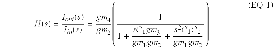
- From this equation, the three independent biquad parameters of DC gain, −3 dB cutoff frequency ω c, and quality factor Q can be inferred:

- To achieve programmable DC gain the present implementation adjusts gm 4 since gm4 is the only parameter which controls gain without affecting either the cutoff frequency or Q. Note that gm4 is absent in both EQ 3 and EQ 4, above. The capacitors C1 and C2 are implemented as binary weighted capacitor arrays in parallel, similar to that illustrated in FIG. 2. A digital code output by the
state machine 130 is sent to terminals b0 . . . b4 to set a specific capacitance value. - The fixed-gm transconductors (gm 1, gm2, gm3) may be implemented as illustrated by the transistor level diagram of FIG. 5. The programmable gm-transconductance block (gm4) may be implemented as a parallel connection of eight unit cells, one of which is shown in FIG. 6.
- The gain setting of gm 4 is dictated by how many of the eight unit cells are “on”. The four possible settings are 1, 2, 4 or 8, corresponding to 0 dB, 6 dB, 12 dB and 18 dB of gain, relative to the transconductance of a single unit cell. Note that, as illustrated in FIG. 6, when a transconductor unit cell is “off”, the NMOS currents are switched to the positive power supply rail, rather than shut off. Applying the same DC bias in all of the NMOS transistors in each unit cell ensures that the parasitic capacitance contributed by the input of gm4 remains independent of the gain setting.
- The choice between the two biquad topologies described above is determined by considering signal scaling at the internal node. In order to maximize the dynamic range, the signal power at all four signal nodes of the filter should be kept within reasonable limits. Preferably, the present invention uses the topology of FIG. 4(A) for the first,
low Q biquad 102, and the topology of FIG. 4(B) for the second,high Q biquad 104. From standard filter theory, in order to achieve a four-pole Butterworth response, the Q of these two biquads is 0.541 and 1.307, respectively. - One advantage of the present current-mode topology is that linearity is preserved even in the presence of a nonlinear transconductor. Individually, the transconductors do not have particularly linear voltage-to-current characteristics. However, in the context of a current-in/current-out topology, the nonlinearity of the first current-to-voltage conversion is compensated by the non-linearity of the corresponding voltage-to-current conversion. More precisely, the current-mode biquad filter acts like a cascoded current mirror in the passband, and cascoded current mirrors have very good linearity.
- FIG. 7A is a block diagram of a replica biquad tuning circuit according to an embodiment of the present invention. The replica tuning circuit includes the
replica biquad filter 110, thephase detector 120, and thestate machine 130. Thephase detector 120 is shown in greater detail and includes apre-amplifier 700, acomparator 710, an input capacitor pair COS, and a pair of phase signals φ1 and φ2. Thepre-amplifier 700 has AC coupling on its input. Twoswitches 701, 702 are connected across thepre-amplifier 700, and are controlled by the phase signal φ1, which is generated by thestate machine 130. The polarity of thepre-amplifier 700 is illustrated in FIG. 7(A). The negative output is connected to the positive input via oneswitch 701, and the positive output is connected to the negative input via the other switch 702. - FIG. 7B is a timing diagram of the replica tuning circuit illustrated in FIG. 7A. The first signal represents an 8 MHz clock, which is preferably implemented as a square wave with 50% duty cycle, and serves as the input to the replica biquad filter. The second signal represents the output of the replica filter when its phase shift is exactly 90 degrees at 8 MHz. Note that the output is not only phase-shifted, but the harmonics of the square wave are filtered as well, resulting in a more sinusoidal waveform. The third signal represents the offset sampling phase; specifically, switches 701 and 702 are closed when the φ1 waveform is high, and open when the φ1 waveform is low. Finally, the fourth signal represents the comparator strobe phase; specifically, the comparator is strobed on the rising edge of φ2. The
numbers 0 through 7 and labeled ‘count’ refer to the ‘count’ variable in the state diagram (FIG. 8). These count increments are identified in the timing diagram in order to explain the operation of the state diagram in FIG. 8. - The switched-capacitor pre-amplifier of the
phase detector 120 serves two functions: (1) it provides about 12 dB of gain to overcome the DC offset of the comparator; and (2) switched-capacitor operation cancels the DC offset present at the output of the replica biquad, plus a portion of the input-referred offset of the comparator itself. To understand this DC-offset cancellation scheme more clearly, consider the operation of the phase detector when the replica biquad output contains a DC offset. First, note that the input and output of the replica biquad can be expressed:
- where the signal sizes at input and output are normalized to unit amplitude, f is the reference frequency (8 MHz), φ is the phase deviation from an ideal 90° (π/2) and V DC is the DC offset. During the sample phase φ1, the pre-amplifier inputs and outputs are shorted together and the voltage on the offset storage capacitors COS track the output of the replica biquad. If the falling edge of φ1 is assigned to time t=0, then the voltage stored on the capacitors at t=0 (when the sampling switches are opened) is:
- V(C OS)=sin(−φ)+V DC (EQ 6)
- Subsequently, the input to the pre-amplifier will equal the replica output minus V(C OS), or

- from which it can be seen that the DC offset is effectively cancelled. Finally, at the rising edge of the compare phase φ2, the signal has advanced 180 degrees, so the pre-amplifier input at the instant of strobing the comparator is:

- Note that this technique not only cancels the DC offset, but yields an additional gain of 2 in front of the preamp, which offers further immunity to comparator offsets. Circuit simulations indicate that without this DC offset cancellation approach, the accumulated DC offsets in the circuit are enough to cause at least 1 LSB of uncertainty in the capacitor setting. The DC offset cancellation approach described above solves this problem. In summary, as illustrated in the circuit and timing diagrams, the entire process makes the comparator sensitive to the phase difference from 90°, without being sensitive to the DC offset.
- The
state machine 130 is clocked at 32 MHz, and generates the 8 MHz replica biquad filter input square wave, as well as the clock phases φ1 (the sample phase) and φ2 (the compare phase). Note that all of the transitions of the 8 MHz clock and of both the sample and compare phases occur on rising edges of the 32 MHz clock (the first eight of these rising edges are drawn as dotted lines in the figure); this alignment facilitates design of the logic in the state machine, since positive-edge-triggered synchronous logic can generate these three clocks with very good phase accuracy. - FIG. 8 is a state diagram of a capacitor
selection state machine 130 according to an embodiment of the present invention. Each state illustrated includes pseudo code, which is an example programming structure for implementing each of the illustrated states. As an example programming structure, the pseudo code for each state is not intended to be a compilable or executable portion of code, but as an example programming structure that provides a non-limiting implementation of a process or method consistent with the present invention. - Preferably, the present invention is implemented in a packet based system such as an 802.11a/b/g system. If a system is packet-based, it receives packets periodically, which tend to be on the order of 1 ms long. The receiver is turned on and off with each received packet, and therefore the receiver is turned on with a certain frequency. The present invention tunes the capacitors each time the receiver is turned “on.” Once the filter calibration procedure converges, it holds the correct capacitor settings to tune the filter to the selected cut-off frequency. The held settings are correct, accounting for thermal drift or other variances, for at least one millisecond.
- When the receiver is restarted, the filter determines the right settings by determining when there is a transition from a series of “up” requests to a “down” request, or vice versa. That is, if there are a series of up adjustments, and then a down, the filter must be on the transition point between up and down, and it picks the higher state. This type of selection makes the calibration more repeatable. The starting point for the next calibration cycle is just above the same position of the last calibration.
- Thus, the calibration can be performed once every millisecond. The actual timing of the calibrations, however, may be highly dependent on what kind of traffic the network is experiencing. In a typical case, a packet is about 1 ms long and the frequency that the packets are being received is unimportant, since the filter does this calibration at the beginning of each received packet (e.g., each request to receive), and the filter maintains that calibration for the duration of the receive packet.
- The behavior of the state machine can be summarized as follows. The state machine begins operation immediately after the receiver is turned on. At this point, the state machine waits a programmable
duration period wait_I 810 in order for the power-on transients to settle. Next, the state machine enters aloop 820/830 in which it performs the offset-sampling and phase comparison operation described with respect to the timing diagram of FIG. 7B. At each comparator decision, the state machine adjusts the capacitor settings, either incrementing the capacitance if the phase is less than 90°, or decrementing it if the phase is greater than 90°. The state machine produces a programmable number of comparator strobes (maxstrobes). At this point, it is assumed that the point of 90° phase shift has been found, and the comparator is oscillating between its two possible states. The state machine then picks the higher of the two capacitor settings which straddle the transition between up and down, then shuts down thereplica filter circuit 840, and holds the final capacitor setting for the duration of the receivepacket 850. The time duration occupied by the capacitor selection is programmable through the parameter maxstrobes. With a careful selection of parameters, the algorithm occupies a maximum of 2 μsec, and typically takes less than 0.5 μsec. In either case, the calibration procedure converges to a final capacitance setting before data is expected to be received. Furthermore, since a typical receive packet is on the order of 1 ms long, the average power dissipation of the replica tuning circuit is effectively zero. - As described herein, the baseband filter architecture of the present invention contains several innovations over previous implementations. Compared to an off-chip passive filter, the integrated approach possesses four distinct advantages: (1) cost advantages associated with the high level of integration; (2) with careful chip layout, the on-chip components can be expected to match each other better than off-chip components, resulting in better I-Q amplitude and phase matching performance; (3) better cut-off frequency control; and (4) routing signals off-chip is an inconvenience due to increased pin count (for instance, previous passive filter implementations require 12 or more additional I/O pins) and the associated degradation of signal integrity. The tuning system chosen for this design possesses several advantages over previous implementations of integrated filters. Compared to continuous-time tuned filters (for example, PLL-based), in the interval while signals are being received the digital capacitor selection approach does not perturb the signal path; in fact, it does not even dissipate any power. Compared to approaches which tune the gm's in a gm-C filter, the capacitor-tuning approach does not suffer changes in linearity performance across the tuning range.
- The present invention is preferably implemented in a direct conversion receiver, however, the processes and technologies discussed herein may be applied to other receiver types. In describing preferred embodiments of the present invention illustrated in the drawings, specific terminology is employed for the sake of clarity. However, the present invention is not intended to be limited to the specific terminology so selected, and it is to be understood that each specific element includes all technical equivalents which operate in a similar manner. For example, when describing a digitally controlled capacitor array, any other equivalent device, such as a analog or other variable capacitor, or other device having an equivalent function or capability, whether or not listed herein, may be substituted therewith. Furthermore, the inventors recognize that newly developed technologies not now known may also be substituted for the described parts and still not depart from the scope of the present invention. All other described items, including, but not limited to transconductance blocks (gms), op-amps, state machines, clocks, transistors and other electrical components, etc should also be consider in light of any and all available equivalents.
- Portions of the present invention may be conveniently implemented using a conventional general purpose or a specialized digital computer or microprocessor programmed according to the teachings of the present disclosure, as will be apparent to those skilled in the computer art.
- Appropriate software coding can readily be prepared by skilled programmers based on the teachings of the present disclosure, as will be apparent to those skilled in the software art. The invention may also be implemented by the preparation of application specific integrated circuits or by interconnecting an appropriate network of conventional component circuits, as will be readily apparent to those skilled in the art based on the present disclosure.
- Included in the programming (software) of the general/specialized computer or microprocessor are software modules for implementing the teachings of the present invention, including, but not limited to, recognizing packet receptions, tuning capacitors and other electrical components, recognizing phase shifts, etc.
- Those skilled in the art will appreciate that various adaptations and modifications of the just-described preferred embodiments can be configured without departing from the scope and spirit of the invention. Therefore, it is to be understood that, within the scope of the appended claims, the invention may be practiced other than as specifically described herein.
Claims (21)
Priority Applications (4)
| Application Number | Priority Date | Filing Date | Title |
|---|---|---|---|
| US10/138,848 US7051063B2 (en) | 2002-05-03 | 2002-05-03 | Integrated low power channel select filter having high dynamic range and bandwidth |
| AU2003234450A AU2003234450A1 (en) | 2002-05-03 | 2003-05-02 | An integrated low power channel select filter having high dynamic range and bandwidth |
| TW092112135A TWI283106B (en) | 2002-05-03 | 2003-05-02 | An integrated low power channel select filter having high dynamic range and bandwidth |
| PCT/US2003/013782 WO2003094348A1 (en) | 2002-05-03 | 2003-05-02 | An integrated low power channel select filter having high dynamic range and bandwidth |
Applications Claiming Priority (1)
| Application Number | Priority Date | Filing Date | Title |
|---|---|---|---|
| US10/138,848 US7051063B2 (en) | 2002-05-03 | 2002-05-03 | Integrated low power channel select filter having high dynamic range and bandwidth |
Publications (2)
| Publication Number | Publication Date |
|---|---|
| US20030207679A1 true US20030207679A1 (en) | 2003-11-06 |
| US7051063B2 US7051063B2 (en) | 2006-05-23 |
Family
ID=29269434
Family Applications (1)
| Application Number | Title | Priority Date | Filing Date |
|---|---|---|---|
| US10/138,848 Expired - Fee Related US7051063B2 (en) | 2002-05-03 | 2002-05-03 | Integrated low power channel select filter having high dynamic range and bandwidth |
Country Status (4)
| Country | Link |
|---|---|
| US (1) | US7051063B2 (en) |
| AU (1) | AU2003234450A1 (en) |
| TW (1) | TWI283106B (en) |
| WO (1) | WO2003094348A1 (en) |
Cited By (14)
| Publication number | Priority date | Publication date | Assignee | Title |
|---|---|---|---|---|
| US20040120421A1 (en) * | 2002-12-18 | 2004-06-24 | Filipovic Daniel F. | Supporting multiple wireless protocols in a wireless device |
| US20040209591A1 (en) * | 2003-04-21 | 2004-10-21 | Quorum Systems, Inc. | Reconfigurable baseband filter |
| US20060079299A1 (en) * | 2004-10-07 | 2006-04-13 | Speed Tech Corp. | Sliding structure for a mobile device |
| US20080218255A1 (en) * | 2004-12-13 | 2008-09-11 | Matsushita Electric Industrial Co., Ltd. | Filter Characteristic Adjusting Apparatus and Filter Characteristic Adjusting Method |
| US20080246458A1 (en) * | 2007-04-06 | 2008-10-09 | Analog Devices, Inc. | Digital compensation tuning for switching power supply control |
| US7769799B2 (en) | 2005-05-13 | 2010-08-03 | Atmel Corporation | Discrete-time analog, digitally programmable filter and method |
| US20100323651A1 (en) * | 2009-06-23 | 2010-12-23 | Qualcomm Incorporated | Tunable adaptive filter with variable gain trans-conductance stage |
| EP2675080A1 (en) * | 2012-06-15 | 2013-12-18 | Imec | A phased-array receiver for mm-wave applications |
| US20140180052A1 (en) * | 2011-06-20 | 2014-06-26 | The Regents Of The University Of California | Neural recording system |
| US8872580B2 (en) | 2012-07-16 | 2014-10-28 | King Fahd University Of Petroleum And Minerals | Reconfigurable high-order integrated circuit filters |
| US20140330102A1 (en) * | 2013-05-03 | 2014-11-06 | The Florida International University Board Of Trustees | Low noise analog electronic circuit design for recording peripheral nerve activity |
| US20150312835A1 (en) * | 2014-04-28 | 2015-10-29 | Aruba Networks, Inc. | Distributed radio management |
| US10267896B1 (en) * | 2014-08-21 | 2019-04-23 | National Technology & Engineering Solutions Of Sandia, Llc | Variable bandwidth filter |
| WO2022146640A1 (en) * | 2020-12-29 | 2022-07-07 | Qualcomm Incorporated | Complementary current-mode biquad with high linearity |
Families Citing this family (8)
| Publication number | Priority date | Publication date | Assignee | Title |
|---|---|---|---|---|
| JP3308508B2 (en) * | 1999-06-15 | 2002-07-29 | 松下電器産業株式会社 | Ladder type filter, analog equalizer and signal regeneration system |
| JP2005328272A (en) * | 2004-05-13 | 2005-11-24 | Nec Electronics Corp | Pll circuit and frequency setting circuit using the same |
| DE102004030229A1 (en) * | 2004-06-23 | 2006-01-19 | Infineon Technologies Ag | Radio-pollutable data carrier |
| US7924068B2 (en) * | 2005-11-29 | 2011-04-12 | Nec Corporation | Automatic adjustment circuit, and filter circuit |
| US20100066442A1 (en) * | 2008-09-15 | 2010-03-18 | Fenghao Mu | Method and Apparatus for Tunable Current-Mode Filtering |
| US8452253B2 (en) | 2010-07-20 | 2013-05-28 | Broadcom Corporation | Compact low-power receiver including transimpedance amplifier, digitally controlled interface circuit, and low pass filter |
| JP2013219569A (en) * | 2012-04-10 | 2013-10-24 | Seiko Epson Corp | Transconductance adjustment circuit, circuit device, and electronic apparatus |
| US9160309B2 (en) | 2013-12-11 | 2015-10-13 | Qualcomm Incorporated | Area efficient baseband filter |
Citations (6)
| Publication number | Priority date | Publication date | Assignee | Title |
|---|---|---|---|---|
| US5072298A (en) * | 1989-09-28 | 1991-12-10 | Kabushiki Kaisha Toshiba | Auto-tuning circuit for an active filter used in video signal processing |
| US5245565A (en) * | 1991-07-31 | 1993-09-14 | International Microelectronic Products | Digitally programmable linear phase filter having phase equalization |
| US6097244A (en) * | 1998-12-17 | 2000-08-01 | Centillium Communications, Inc. | Highly-linear continuous-time filter for a 3-volt supply with PLL-controlled resistor and digitally-controlled capacitor |
| US20020011896A1 (en) * | 2000-07-12 | 2002-01-31 | Akio Yokoyama | Automatic filter tuning control system |
| US6417737B1 (en) * | 1999-10-21 | 2002-07-09 | Broadcom Corporation | Adaptive radio transceiver with low noise amplification |
| US6738601B1 (en) * | 1999-10-21 | 2004-05-18 | Broadcom Corporation | Adaptive radio transceiver with floating MOSFET capacitors |
-
2002
- 2002-05-03 US US10/138,848 patent/US7051063B2/en not_active Expired - Fee Related
-
2003
- 2003-05-02 TW TW092112135A patent/TWI283106B/en not_active IP Right Cessation
- 2003-05-02 WO PCT/US2003/013782 patent/WO2003094348A1/en not_active Application Discontinuation
- 2003-05-02 AU AU2003234450A patent/AU2003234450A1/en not_active Abandoned
Patent Citations (9)
| Publication number | Priority date | Publication date | Assignee | Title |
|---|---|---|---|---|
| US5072298A (en) * | 1989-09-28 | 1991-12-10 | Kabushiki Kaisha Toshiba | Auto-tuning circuit for an active filter used in video signal processing |
| US5245565A (en) * | 1991-07-31 | 1993-09-14 | International Microelectronic Products | Digitally programmable linear phase filter having phase equalization |
| US5325317A (en) * | 1991-07-31 | 1994-06-28 | International Microelectronic Products | Digitally programmable linear phase filter having phase equalization |
| US5463349A (en) * | 1991-07-31 | 1995-10-31 | Imp, Inc. | Programmable operation transconductance amplifier |
| US6097244A (en) * | 1998-12-17 | 2000-08-01 | Centillium Communications, Inc. | Highly-linear continuous-time filter for a 3-volt supply with PLL-controlled resistor and digitally-controlled capacitor |
| US6417737B1 (en) * | 1999-10-21 | 2002-07-09 | Broadcom Corporation | Adaptive radio transceiver with low noise amplification |
| US20030067359A1 (en) * | 1999-10-21 | 2003-04-10 | Broadcom Corporation | Adaptive radio transceiver with a local oscillator |
| US6738601B1 (en) * | 1999-10-21 | 2004-05-18 | Broadcom Corporation | Adaptive radio transceiver with floating MOSFET capacitors |
| US20020011896A1 (en) * | 2000-07-12 | 2002-01-31 | Akio Yokoyama | Automatic filter tuning control system |
Cited By (24)
| Publication number | Priority date | Publication date | Assignee | Title |
|---|---|---|---|---|
| US20040120421A1 (en) * | 2002-12-18 | 2004-06-24 | Filipovic Daniel F. | Supporting multiple wireless protocols in a wireless device |
| US7106816B2 (en) * | 2002-12-18 | 2006-09-12 | Qualcomm Incorporated | Supporting multiple wireless protocols in a wireless device |
| US20040209591A1 (en) * | 2003-04-21 | 2004-10-21 | Quorum Systems, Inc. | Reconfigurable baseband filter |
| US7676211B2 (en) * | 2003-04-21 | 2010-03-09 | Spreadtrum Communications Inc. | Reconfigurable baseband filter |
| US20060079299A1 (en) * | 2004-10-07 | 2006-04-13 | Speed Tech Corp. | Sliding structure for a mobile device |
| US20080218255A1 (en) * | 2004-12-13 | 2008-09-11 | Matsushita Electric Industrial Co., Ltd. | Filter Characteristic Adjusting Apparatus and Filter Characteristic Adjusting Method |
| US7688059B2 (en) * | 2004-12-13 | 2010-03-30 | Panasonic Corporation | Filter characteristic adjusting apparatus and filter characteristic adjusting method |
| US7769799B2 (en) | 2005-05-13 | 2010-08-03 | Atmel Corporation | Discrete-time analog, digitally programmable filter and method |
| US20080246458A1 (en) * | 2007-04-06 | 2008-10-09 | Analog Devices, Inc. | Digital compensation tuning for switching power supply control |
| US7876083B2 (en) * | 2007-04-06 | 2011-01-25 | Semiconductor Components Industries, L.L.C. | Digital compensation tuning for switching power supply control |
| US20100323651A1 (en) * | 2009-06-23 | 2010-12-23 | Qualcomm Incorporated | Tunable adaptive filter with variable gain trans-conductance stage |
| US9602079B2 (en) * | 2009-06-23 | 2017-03-21 | Qualcomm Incorporated | Tunable adaptive filter with variable gain trans-conductance stage |
| US20140180052A1 (en) * | 2011-06-20 | 2014-06-26 | The Regents Of The University Of California | Neural recording system |
| US9538928B2 (en) * | 2011-06-20 | 2017-01-10 | The Regents Of The University Of California | Neural recording system |
| US9020457B2 (en) | 2012-06-15 | 2015-04-28 | Imec | Phased-array receiver for mm-wave applications |
| EP2675080A1 (en) * | 2012-06-15 | 2013-12-18 | Imec | A phased-array receiver for mm-wave applications |
| US8872580B2 (en) | 2012-07-16 | 2014-10-28 | King Fahd University Of Petroleum And Minerals | Reconfigurable high-order integrated circuit filters |
| US8896371B2 (en) | 2012-07-16 | 2014-11-25 | King Fahd University Of Petroleum And Minerals | Reconfigurable high-order integrated circuit filters |
| US20140330102A1 (en) * | 2013-05-03 | 2014-11-06 | The Florida International University Board Of Trustees | Low noise analog electronic circuit design for recording peripheral nerve activity |
| US9662025B2 (en) * | 2013-05-03 | 2017-05-30 | The Florida International University Board Of Trustees | Low noise analog electronic circuit design for recording peripheral nerve activity |
| US20150312835A1 (en) * | 2014-04-28 | 2015-10-29 | Aruba Networks, Inc. | Distributed radio management |
| US9565627B2 (en) * | 2014-04-28 | 2017-02-07 | Aruba Networks, Inc. | Distributed radio management |
| US10267896B1 (en) * | 2014-08-21 | 2019-04-23 | National Technology & Engineering Solutions Of Sandia, Llc | Variable bandwidth filter |
| WO2022146640A1 (en) * | 2020-12-29 | 2022-07-07 | Qualcomm Incorporated | Complementary current-mode biquad with high linearity |
Also Published As
| Publication number | Publication date |
|---|---|
| TWI283106B (en) | 2007-06-21 |
| WO2003094348A1 (en) | 2003-11-13 |
| US7051063B2 (en) | 2006-05-23 |
| AU2003234450A1 (en) | 2003-11-17 |
| TW200401501A (en) | 2004-01-16 |
Similar Documents
| Publication | Publication Date | Title |
|---|---|---|
| US7051063B2 (en) | Integrated low power channel select filter having high dynamic range and bandwidth | |
| Giannini et al. | Flexible baseband analog circuits for software-defined radio front-ends | |
| US6417737B1 (en) | Adaptive radio transceiver with low noise amplification | |
| US6920311B2 (en) | Adaptive radio transceiver with floating MOSFET capacitors | |
| US7860454B2 (en) | Adaptive radio transceiver with a power amplifier | |
| US7863972B2 (en) | Self-calibration of continuous-time filters and systems comprising such filters | |
| US20050181754A1 (en) | Adaptive radio transceiver with calibration | |
| US6885181B1 (en) | Calibration circuit | |
| US7064557B2 (en) | Calibration circuit and method for filter bandwidth which is parasitic capacitance sensitive or insensitive | |
| US6891436B2 (en) | Transconductance varying circuit of transconductor circuit, varying bandwidth filter circuit using the same and digital tuning circuit of transconductor-capacitor filter | |
| EP0732807B1 (en) | Controllable filter arrangement | |
| KR100399166B1 (en) | Adjustable resistance device with control circuit | |
| US20040169532A1 (en) | Device for controlling a frequency response by scaling an impedance | |
| D'Amico et al. | A 1.2 V-21dBm OIP3 4/sup th/-order active-g/sub m/-RC reconfigurable (UMTS/WLAN) filter with on-chip tuning designed with an automatic tool | |
| EP1629594A1 (en) | Improvements in or relating to transconductor circuits | |
| US6873205B1 (en) | Active continuous-time filter with increased dynamic range in the presence of blocker signals | |
| WO2008010331A1 (en) | Output conductance automatic regulation circuit of differential current output type circuit and filter circuit | |
| WO2002035756A2 (en) | Active continuous-time filter with increased dynamic range in the presence of blocker signals | |
| Giannini et al. | Implementations of Flexible Filters for Sdr Front End |
Legal Events
| Date | Code | Title | Description |
|---|---|---|---|
| AS | Assignment |
Owner name: ATHEROS COMMUNICATIONS, INC., CALIFORNIA Free format text: ASSIGNMENT OF ASSIGNORS INTEREST;ASSIGNORS:KACZYNSKI, BRIAN;MEHTA, SRENIK;REEL/FRAME:012880/0010 Effective date: 20020501 |
|
| FEPP | Fee payment procedure |
Free format text: PAT HOLDER NO LONGER CLAIMS SMALL ENTITY STATUS, ENTITY STATUS SET TO UNDISCOUNTED (ORIGINAL EVENT CODE: STOL); ENTITY STATUS OF PATENT OWNER: LARGE ENTITY |
|
| FPAY | Fee payment |
Year of fee payment: 4 |
|
| AS | Assignment |
Owner name: QUALCOMM ATHEROS, INC., CALIFORNIA Free format text: MERGER;ASSIGNOR:ATHEROS COMMUNICATIONS, INC.;REEL/FRAME:026599/0360 Effective date: 20110105 |
|
| AS | Assignment |
Owner name: QUALCOMM INCORPORATED, CALIFORNIA Free format text: ASSIGNMENT OF ASSIGNORS INTEREST;ASSIGNOR:QUALCOMM ATHEROS, INC.;REEL/FRAME:029328/0052 Effective date: 20121022 |
|
| FPAY | Fee payment |
Year of fee payment: 8 |
|
| FEPP | Fee payment procedure |
Free format text: PAYOR NUMBER ASSIGNED (ORIGINAL EVENT CODE: ASPN); ENTITY STATUS OF PATENT OWNER: LARGE ENTITY Free format text: PAYER NUMBER DE-ASSIGNED (ORIGINAL EVENT CODE: RMPN); ENTITY STATUS OF PATENT OWNER: LARGE ENTITY |
|
| FEPP | Fee payment procedure |
Free format text: MAINTENANCE FEE REMINDER MAILED (ORIGINAL EVENT CODE: REM.) |
|
| LAPS | Lapse for failure to pay maintenance fees |
Free format text: PATENT EXPIRED FOR FAILURE TO PAY MAINTENANCE FEES (ORIGINAL EVENT CODE: EXP.) |
|
| STCH | Information on status: patent discontinuation |
Free format text: PATENT EXPIRED DUE TO NONPAYMENT OF MAINTENANCE FEES UNDER 37 CFR 1.362 |
|
| FP | Lapsed due to failure to pay maintenance fee |
Effective date: 20180523 |