US20040150737A1 - Solid state imager arrangements - Google Patents
Solid state imager arrangements Download PDFInfo
- Publication number
- US20040150737A1 US20040150737A1 US10/734,597 US73459703A US2004150737A1 US 20040150737 A1 US20040150737 A1 US 20040150737A1 US 73459703 A US73459703 A US 73459703A US 2004150737 A1 US2004150737 A1 US 2004150737A1
- Authority
- US
- United States
- Prior art keywords
- register
- multiplication
- charge
- arrangement
- signal charge
- Prior art date
- Legal status (The legal status is an assumption and is not a legal conclusion. Google has not performed a legal analysis and makes no representation as to the accuracy of the status listed.)
- Granted
Links
- 239000007787 solid Substances 0.000 title claims abstract description 6
- 238000012546 transfer Methods 0.000 claims description 27
- 230000004888 barrier function Effects 0.000 claims description 22
- 238000001514 detection method Methods 0.000 description 8
- 238000005036 potential barrier Methods 0.000 description 6
- 238000000034 method Methods 0.000 description 4
- 238000012545 processing Methods 0.000 description 4
- 230000005855 radiation Effects 0.000 description 3
- 230000008901 benefit Effects 0.000 description 2
- 238000004891 communication Methods 0.000 description 2
- 238000005286 illumination Methods 0.000 description 2
- 230000010354 integration Effects 0.000 description 2
- 238000012986 modification Methods 0.000 description 2
- 230000004048 modification Effects 0.000 description 2
- 229910021420 polycrystalline silicon Inorganic materials 0.000 description 2
- 229920005591 polysilicon Polymers 0.000 description 2
- 230000008569 process Effects 0.000 description 2
- 230000009467 reduction Effects 0.000 description 2
- 230000004044 response Effects 0.000 description 2
- 230000003321 amplification Effects 0.000 description 1
- 238000013459 approach Methods 0.000 description 1
- 239000000969 carrier Substances 0.000 description 1
- 238000001444 catalytic combustion detection Methods 0.000 description 1
- 239000002800 charge carrier Substances 0.000 description 1
- 238000006243 chemical reaction Methods 0.000 description 1
- 230000005574 cross-species transmission Effects 0.000 description 1
- 230000003111 delayed effect Effects 0.000 description 1
- 230000001419 dependent effect Effects 0.000 description 1
- 230000001771 impaired effect Effects 0.000 description 1
- 239000007943 implant Substances 0.000 description 1
- 238000001208 nuclear magnetic resonance pulse sequence Methods 0.000 description 1
- 238000003199 nucleic acid amplification method Methods 0.000 description 1
- 238000005192 partition Methods 0.000 description 1
- 238000000819 phase cycle Methods 0.000 description 1
- 230000002250 progressing effect Effects 0.000 description 1
- 238000005215 recombination Methods 0.000 description 1
- 230000006798 recombination Effects 0.000 description 1
- 230000035945 sensitivity Effects 0.000 description 1
- 229910052710 silicon Inorganic materials 0.000 description 1
- 239000010703 silicon Substances 0.000 description 1
- 230000001360 synchronised effect Effects 0.000 description 1
- 230000007704 transition Effects 0.000 description 1
Images


Classifications
-
- H—ELECTRICITY
- H01—ELECTRIC ELEMENTS
- H01L—SEMICONDUCTOR DEVICES NOT COVERED BY CLASS H10
- H01L29/00—Semiconductor devices adapted for rectifying, amplifying, oscillating or switching, or capacitors or resistors with at least one potential-jump barrier or surface barrier, e.g. PN junction depletion layer or carrier concentration layer; Details of semiconductor bodies or of electrodes thereof ; Multistep manufacturing processes therefor
- H01L29/66—Types of semiconductor device ; Multistep manufacturing processes therefor
- H01L29/68—Types of semiconductor device ; Multistep manufacturing processes therefor controllable by only the electric current supplied, or only the electric potential applied, to an electrode which does not carry the current to be rectified, amplified or switched
- H01L29/76—Unipolar devices, e.g. field effect transistors
- H01L29/762—Charge transfer devices
- H01L29/765—Charge-coupled devices
- H01L29/768—Charge-coupled devices with field effect produced by an insulated gate
- H01L29/76816—Output structures
-
- H—ELECTRICITY
- H01—ELECTRIC ELEMENTS
- H01L—SEMICONDUCTOR DEVICES NOT COVERED BY CLASS H10
- H01L27/00—Devices consisting of a plurality of semiconductor or other solid-state components formed in or on a common substrate
- H01L27/14—Devices consisting of a plurality of semiconductor or other solid-state components formed in or on a common substrate including semiconductor components sensitive to infrared radiation, light, electromagnetic radiation of shorter wavelength or corpuscular radiation and specially adapted either for the conversion of the energy of such radiation into electrical energy or for the control of electrical energy by such radiation
- H01L27/144—Devices controlled by radiation
- H01L27/146—Imager structures
- H01L27/148—Charge coupled imagers
- H01L27/14806—Structural or functional details thereof
Definitions
- This invention relates to solid-state imager arrangements and more particularly to arrangements in which signal charge multiplication is implemented.
- signal charge representative of incident radiation is accumulated in an array of pixels over an image area. Following an integration period, signal charge is transferred to an output register by applying appropriate clocking or drive pulses to control electrodes. The signal charge is then read out from the output register and applied to a charge detection circuit to produce a voltage, which is representative of the amount of signal charge.
- CCD charge coupled device
- GB-A-2323471 discloses a CCD imager arrangement in which signal charge multiplication is obtained by providing a separate multiplication register following the output register. Charge is transferred through high field regions in elements of the multiplication register, thus accelerating the signal charge carriers and generating additional carriers through impact ionisation. As carrier multiplication occurs outside the conventional CCD structure itself, both the operation of the multiplication register and the CCD imager may be optimised without compromising the performance of one for the sake of the other.
- the present invention seeks to provide an improved solid-state imager arrangement.
- a solid state imager arrangement comprising: an image area, an output register which receives signal charge from the image area, a separate multiplication register into which signal charge from the output register is transferred, means for obtaining signal charge multiplication by transferring the charge through a sufficiently high field in elements of the multiplication register, and an additional register into which excess signal charge is transferred.
- the invention is particularly suitable for arrangements in which the solid-state imager is a CCD imager but it may be applicable to other types of solid-state device in which packets of signal charge are transferred into an output register.
- the excess signal charge is that charge originating from the image area, which does not pass entirely through the charge multiplication register.
- a drain region may be included which accepts charge exceeding a threshold value to avoid saturation.
- the present invention has realised that although the previously proposed structure offers good performance, it is possible to enhance it still further.
- the inclusion of an additional register to accept excess charge means that in circumstances where the well capacities of the multiplication register are likely to be exceeded, some of the signal charge originating from the image area is diverted away from the multiplication part of the arrangement. Instead, this excess signal charge is transferred to the additional register, which is a structure also capable of holding charge packets, which may be controllably moved through the additional register. The remaining charge, which passes through each multiplication stage, may then be recombined with the excess charge from the additional register.
- the signal charge packet may be reconstituted by appropriate synchronised clocking of the two register outputs to transfer corresponding charge packets from the multiplication and additional registers to a single charge detection circuit simultaneously.
- the combining step is conveniently carried out before any further processing of the signal charge is carried out but it could be implemented at a later stage in the processing sequence, for example after charge has been converted at separate charge detection circuits or following conversion into video output. It may not always be necessary to synchronise the multiplication and additional register readouts providing provision is made for combining the signal from charge packets originating from the same pixel.
- the dynamic range may be increased in comparison with the previous arrangement.
- charge is lost to preserve image resolution at high illumination levels.
- the additional register acts as an overflow to store the excess signal charge, which can then be usefully added back to the multiplied charge instead of being discarded. This gives the capability for the same imager arrangement to be used for both low light conditions and daylight conditions. It also permits dark and bright images in a scene to be detected simultaneously without loss of resolution in the high intensity regions.
- the dynamic range capability of a CCD is often described by the ratio of the saturation signal to the read noise.
- the transfer curve is linear and saturation is determined by the charge handling capability of the output circuit or of the elements of the multiplication register which is typically only a few times greater than that of the pixel. Since gain implemented by the multiplication register may be 200 times or greater, the saturation signal may represent less than 1% of the well capacity of the pixel. By employing the invention, however, the whole range of pixel well capacity may be used, giving the consequent increase in dynamic range.
- the transfer of excess signal charge into the additional register may be accomplished by passive means or by active means, such as a gate electrode structure to which control signals are applied.
- the signal charge from the output register is applied to the multiplication register.
- the charge is increased as it is clocked through the multiplication register and undergoes signal multiplication.
- the additional register is located adjacent the multiplication register, separated therefrom by a potential barrier. Excess charge from the multiplication register flows over the barrier and into a corresponding element of the additional register.
- the signal charge from the two registers may be detected on separate amplifiers or combined and detected on a single output as the sum of the two register outputs.
- the multiplication register has a peak capacity N electrons and a gain of G
- the response is linear with a slope of G up to N/G input electrons and then logarithmic to N input electrons.
- all elements of the multiplication register will be full, so gain contribution to the output signal will be fixed and the response will consequently, again, be linear with a slope of 1.
- the dynamic range is effectively extended by a factor of approximately G, but the additional capacity required is only increased by the logarithm of G.
- the excess signal charge may be transferred to the additional register via one or more elements of the multiplication register as described above.
- excess charge is separated from the remainder of the signal charge before the remainder is applied to the multiplication register.
- signal charge may be detected or sampled either before application of the charge packet to the multiplication register or via one or more elements of the multiplication register. Subsequent transfer of the excess signal charge to the additional register may then be carried out depending on the magnitude of signal charge detected. For example, if it is determined that the signal charge in the first element of multiplication register would lead to saturation in the final element of the multiplication register, following amplification as the charge is transferred through the multiplication register, an amount of signal charge suitable to prevent saturation from occurring may be diverted as excess charge to the additional register. In another embodiment, a fixed percentage of the signal charge may always be diverted to the additional register as excess charge, but this may lead to some reduction in the amount of multiplication, which could otherwise be achieved.
- the excess signal charge may simply be that which exceeds a threshold level at some stage in the transfer of the signal charge through the multiplication register.
- the threshold level may be fixed or may be variable to take into account changes in the scene being viewed by the arrangement and/or ambient conditions.
- the arrangement may be such that each element of the multiplication register corresponds to and is in communication with an element in the additional register, with transfer of excess charge being possible from each element in the multiplication register.
- such transfer may only be possible from certain of the elements of the multiplication register, for example from alternate elements or from elements towards the output end of the multiplication register.
- the additional register is located physically close to the multiplication register so as to permit direct transfer of charge between the two via the intervening structure.
- they could be remotely located with respect to one another with charge being transferred via intervening circuitry and clocking techniques.
- the invention is most applicable to an arrangement in which a single multiplication and a single additional register are included.
- a multiplication register may be associated with a plurality of additional registers, which may be arranged in parallel or in a cascade arrangement.
- a plurality of multiplication registers, each with its own additional register or registers may be included in an arrangement to accept signal charge from a single output register.
- FIG. 1 schematically shows a CCD imager arrangement in accordance with the invention
- FIGS. 2 to 4 shows other arrangements in accordance with the invention.
- FIG. 5 shows an element of the multiplication register of FIGS. 1 to 4 ;
- FIG. 6 shows the well potential of the elements of FIG. 5;
- FIG. 7 shows the well potential of the barrier element of FIG. 1;
- FIG. 8 shows a clocking element as may be used with the arrangement of FIGS. 1 to 4 and the well potential at three time intervals;
- FIG. 9 shows the physical register and barrier implant structure of FIGS. 1 to 4 ;
- FIG. 10 shows the physical register and clocked element structure of the clocking element of FIG. 8.
- the embodiments of the invention all involve the use of a multiplication register for multiplying signal charge from a solid-state imager and an additional register arranged to receive excess charge.
- the purpose of the arrangement is to provide a greater dynamic range by providing gain to small levels of charge (low light levels) whilst avoiding providing too much gain to higher levels of charge (high light levels).
- Charge is divided between the multiplication register and the additional register in two ways. First, as described later in relation to FIG. 1, excess charge transfers from each element of the multiplication register to corresponding elements of the additional register. This transfer can be by overspill over a potential barrier (FIG. 7) or by clocked elements (FIG. 8). Second, as described later in relation to FIGS. 2 and 3, excess charge is transferred to the additional register prior to applying charge to the multiplication register.
- the first and second methods of dividing the charge may be used together or separately. The preferred embodiment uses both charge division before the multiplication register and transfer from the multiplication register to the additional register, although these will be described separately for clarity.
- the embodiments start from the premise that, for the portion of the signal from the imager that has, say, greater than 20,000 electrons, no benefit accrues from multiplication.
- This size of signal can be detected efficiently with a conventional charge detection circuit.
- By diversion of excess charge from the gain register into a parallel, non-gain, register only a small proportion of the charge (that which cannot be efficiently detected without gain) is subject to gain.
- the total charge in the gain and the non-gain registers will not be much greater than for a system with no gain, and so the two charge streams may be recombined, since the total is within the range of a single charge detection circuit with a sensitivity only slightly less than would be required with no gain register.
- the streams of charge in the gain (multiplication) and non-gain (additional) registers can be recombined prior to detection.
- the gain register includes a high voltage clock, which is responsible for significant power dissipation when applied to the capacitance of the gain register. Keeping this register small gives useful reduction in power dissipation.
- a CCD imager 1 includes an image area 2 , a store section 3 and an output or readout register 4 .
- the output register 4 is extended linearly to provide a multiplication register 5 , the output of which is connected to a charge detection circuit 6 .
- An additional register 7 having the same number of elements as the multiplication register 5 is located physically adjacent to the multiplication register 5 , an implanted barrier region 8 , shown schematically, being located between the two registers 5 and 7 .
- incident radiation is converted at the image area 2 into signal charge representative of the intensity of radiation, which impinges on the pixel array making up the image area 2 .
- drive pulses are applied to control electrodes 9 to transfer charge accumulated at the pixels of the image area 2 to the store section 3 .
- drive signals are also applied to control electrodes 10 at the store section to cause charge to be transferred row by row towards the output register 4 .
- Multiplication of charge is implemented at each element of the multiplication register 5 .
- High amplitude drive pulses at the rate at which charge is clocked through the output register 4 , are applied to control electrodes 12 to both transfer signal charge from one element to the next adjacent element in the direction shown by the arrow and also to increase the level of signal charge by an amount determined by the amplitude of the drive pulses.
- the output of the multiplication register 5 is applied to the charge detector 6 , this being a multiplied version of the signal charge collected in the output register 4 .
- signal charge multiplication is increased and each signal charge packet stored in the output register 4 undergoes identical multiplication process as each travels through all the elements of the multiplication register 5 .
- signal charge multiplication is controlled by the level of one or more dc potentials applied to the register.
- the potential is variable via control electrodes and/or is non-uniform. If the charge applied to the first element of the multiplication register 5 is reasonably small, so that at the final element 5 the well capacity would only be exceeded by a relatively small amount, transfer via the barrier between the two registers only occurs between elements at the ends of the registers where the charge has undergone the most multiplication, for example, over the last two or three elements. Where a larger signal charge appears at the first element of the multiplication register 5 , then transfer of the excess charge to the additional register 7 occurs over a greater length of the two registers, transfer being possible between each element of the multiplication register 5 and a corresponding element of the additional register 7 .
- the two registers 5 and 7 are clocked in synchronism so that the charge appearing at the final element of the two registers originated with the same packet of signal charge from a common pixel of the image area 2 .
- the outputs of the two registers are then combined at combiner 13 prior to being applied to the charge detector 6 .
- the registers are clocked in synchronism with line timing of a television signal.
- the elements of the multiplication and/or additional registers may have the same charge capacity, or elements nearer the end or ends may have larger charge capacity.
- a control gate structure is disposed between the multiplication register 5 and additional register 7 to control the transfer of excess charge to the latter by applying suitable control pulses.
- a combination of the two approaches may be used.
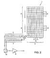
- FIG. 2 illustrates another embodiment of the invention in which a processing circuit is located between the output register 4 and the multiplication register 5 .
- a detector circuit 14 detects the amount of charge for an element from the output register 4 and causes a fixed percentage of that charge to be diverted to the additional register 7 .
- the arrangement is similar to that shown in FIG. 1.
- the charge from the multiplication register and that from the additional register is recombined prior to being applied to charge detector 6 .
- recombination is carried out at a later stage in the processing of the output signal.
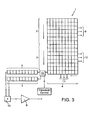
- a threshold circuit 15 replaces the detector circuit 14 and acts on applied signal charge to divert charge exceeding a threshold level to the additional register 7 .
- the threshold level can be fixed or variable. For example, it may be arranged to automatically track changes in ambient temperature or other parameters, or it could be controllably adjustable.
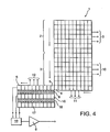
- a device similar to that of FIG. 1 also includes an implanted barrier 8 between a multiplication register 5 and additional register means for carrying excess charge.
- the register means includes two additional registers 16 and 17 also having an implanted barrier 18 between them. Excess charge from additional register 16 is thus transferred to additional register 17 , and outputs of the three registers are recombined at combiner 19 .
- This arrangement may be advantageous where signal charge multiplication is carried out in the first additional register 16 as well as in the multiplication register 5 .
- several additional registers may be arranged in communication with a respective different set of the elements of the multiplication register.
- FIGS. 1 - 4 illustrate the application of the invention to a CCD imager of the Frame Transfer architecture but it is equally applicable to all other architectures e.g. Interline Transfer and Linear imagers.
- each element in the multiplication register comprises a base 20 of p-type silicon, an n-type layer 22 and a dielectric layer 24 . (this describes an n-channel CCD. In principle, the multiplication structures described could also be applied to a p-channel CCD)
- each element On the dielectric layer, each element has four electrodes shown as normal clocked electrodes R ⁇ 1 26 and R ⁇ 3 28 , a DC electrode R ⁇ DC 30 and a high voltage electrode R ⁇ 2 HV 32 .
- the element provides gain by clocking voltages at the electrodes such that a relatively high voltage at electrode R ⁇ 2 HV 32 causes multiplication of charge.
- the clocking of the electrodes is shown further in FIG. 6.
- the element of the multiplication register is made up of four phases although other configurations could be possible.
- R ⁇ 1 and R ⁇ 3 are clocked as normal readout register phases.
- R ⁇ DC is a DC phase that separates R ⁇ 1 from R ⁇ 2 HV.
- R ⁇ 2 HV the multiplication phase, is a clocked phase but using a much greater amplitude than R ⁇ 1 and R ⁇ 3 .
- On the high to low transition of R ⁇ 1 signal originally under R ⁇ 1 will drift to R ⁇ 2 HV.
- the potential on R ⁇ 2 HV is set high enough so that the fields experienced by the electron signal will cause multiplication to take place.
- the total amplified signal can then be transferred to R ⁇ 3 by switching R ⁇ 2 HV low and R ⁇ 3 high.
- the process is repeated through all the gain elements in the multiplication register.
- FIG. 1 One element of the multiplication register 5 , barrier region 8 and additional register 7 are shown. As can be seen, the electrons that have been subject to multiplication collect in R ⁇ 3 well of the multiplication elements 5 . A barrier potential 8 between the multiplication elements and the overspill additional register 7 ensures that electrons do not transfer until the charge in each multiplication element reaches the barrier level, at which point excess charge spills over into wells of the additional register 7 as shown by the arrow.
- the preferred embodiment of the invention is a CCD imager as shown and described in relation to FIGS. 1 to 4 , but modified to include a clocking region in addition to the barrier region 8 .
- the clocking region comprises a group of elements, one such group being shown in FIG. 8.
- Each clocking element is arranged between one element of the multiplication register and one element of the additional register.
- the final electrode of each multiplication element is R ⁇ 3 M and this is separated into two regions by a potential barrier. Charge is transferred into the main region from the previous electrode of the multiplication register. On progressing through successive elements of the multiplication register, charge is increased until the charge in one of the wells under electrode R ⁇ 3 M is sufficient to spill over into the smaller region.
- the clocking element then proceeds through a three-phase cycle.
- the embodiment thus does not gather charge on the opposite side of the barrier potential from R ⁇ 3 M, but moves charge away to R ⁇ 1 C and R ⁇ 2 C from where it is transferred to the additional register. By doing so, the extension of dynamic range is not impaired by the limited capacity of the overspill register with a low potential barrier as in the arrangement of FIG. 7.
- the various regions of the multiplication and overspill register structure may in principle have separate clock connections.
- the Multiplication register these may be designated R ⁇ 1 M, R ⁇ DC, R ⁇ 2 HV, and R ⁇ 3 M (using the suffix M to denote “m”ultiplication and to distinguish from other registers).
- the Overspill register they may be designated R ⁇ 1 O, R ⁇ 2 O and R ⁇ 3 O (using the suffix 0 to denote “o”verspill).
- R ⁇ 1 C, R ⁇ 2 C and R ⁇ 3 C using the suffix C to denote “c”lock).
- R ⁇ 3 C is not shown in FIGS. 8 - 10 but it may exist in a practical application of the invention.
- Separate clock pulses may be applied to all of these connections and variety of clocking schemes devised which would give correct operation of the structures. However there are clear advantages to be obtained both in layout topology and operational simplicity if a number of these clock connections are commoned together.
- R ⁇ 1 M and R ⁇ 1 O may be joined to form a single R ⁇ 1 ; R ⁇ 3 M and R ⁇ 3 O may be joined to form a single R ⁇ 3 .
- the same clock pulse sequence and timing as would be required for a simple multiplication register without overspill may then be used to operate the device with the addition of a single extra clock phase R ⁇ 2 O (typically designated R ⁇ 2 ) which completes a normal 3-phase group of clocks with R ⁇ 1 and R ⁇ 3 .
- These 3 clock phases R ⁇ 1 , R ⁇ 2 and R ⁇ 3 may also be joined to the corresponding clock connections for the standard readout register of the CCD (designated 11 in FIG. 1).
- R ⁇ 1 M, R ⁇ 1 O and R ⁇ 1 C may be joined to form a single R ⁇ 1 ;
- These clocks may also be commoned with those of the standard readout register as before.
- the resulting structure has the same set of connections as the basic structure and will operate with the same set of clock pulses (timing and amplitude).
- the charge, which is clocked to the overspill register is effectively delayed by one element from its associated signal in the multiplication register and allowance must be made for this in recombining the signal e.g. by including an extra element between the multiplication register and the output amplifier.
- the clock connections may be commoned in a number of different ways depending on the layout topology of the CCD e.g. the way in which the multiplication register is folded to minimise device area. As indicated in the figures a single polysilicon electrode may cross 2 or 3 regions to common the clock connection directly.
- polysilicon electrodes for different regions may connect to separate low-resistance bus lines (as is standard for CCDs) and these bus lines may join on chip or be connected to separate bond pads with the connection made externally.
- bus lines as is standard for CCDs
- R ⁇ DC and R ⁇ 2 HV additional connections
Abstract
Description
- This application is a continuation-in-part of application Ser. No. 10/622,109, filed Jul. 18, 2003, which is a continuation of International Application No. PCT/GB02/00138, filed Jul. 14, 2002, and claiming priority to British Application GB 0101301.0 filed Jan. 18, 2001, to which the present application also claims priority. The disclosures of the foregoing applications, together with the disclosures of each and every U.S. and foreign patent and patent application mentioned below are incorporated herein by reference in their entirety.
- This invention relates to solid-state imager arrangements and more particularly to arrangements in which signal charge multiplication is implemented.
- In a typical charge coupled device (CCD) imager, signal charge representative of incident radiation is accumulated in an array of pixels over an image area. Following an integration period, signal charge is transferred to an output register by applying appropriate clocking or drive pulses to control electrodes. The signal charge is then read out from the output register and applied to a charge detection circuit to produce a voltage, which is representative of the amount of signal charge.
- Our previously published patent application, GB-A-2323471 discloses a CCD imager arrangement in which signal charge multiplication is obtained by providing a separate multiplication register following the output register. Charge is transferred through high field regions in elements of the multiplication register, thus accelerating the signal charge carriers and generating additional carriers through impact ionisation. As carrier multiplication occurs outside the conventional CCD structure itself, both the operation of the multiplication register and the CCD imager may be optimised without compromising the performance of one for the sake of the other.
- The present invention seeks to provide an improved solid-state imager arrangement.
- According to the present invention, there is provided a solid state imager arrangement comprising: an image area, an output register which receives signal charge from the image area, a separate multiplication register into which signal charge from the output register is transferred, means for obtaining signal charge multiplication by transferring the charge through a sufficiently high field in elements of the multiplication register, and an additional register into which excess signal charge is transferred.
- The invention is particularly suitable for arrangements in which the solid-state imager is a CCD imager but it may be applicable to other types of solid-state device in which packets of signal charge are transferred into an output register.
- The excess signal charge is that charge originating from the image area, which does not pass entirely through the charge multiplication register. In the previously proposed arrangement, in parts of a scene of high illumination there is a risk that the well capacities in the multiplication register can be exceeded, leading to saturation and loss of image resolution. Thus, a drain region may be included which accepts charge exceeding a threshold value to avoid saturation.
- The present invention has realised that although the previously proposed structure offers good performance, it is possible to enhance it still further. The inclusion of an additional register to accept excess charge means that in circumstances where the well capacities of the multiplication register are likely to be exceeded, some of the signal charge originating from the image area is diverted away from the multiplication part of the arrangement. Instead, this excess signal charge is transferred to the additional register, which is a structure also capable of holding charge packets, which may be controllably moved through the additional register. The remaining charge, which passes through each multiplication stage, may then be recombined with the excess charge from the additional register. For example, the signal charge packet may be reconstituted by appropriate synchronised clocking of the two register outputs to transfer corresponding charge packets from the multiplication and additional registers to a single charge detection circuit simultaneously. The combining step is conveniently carried out before any further processing of the signal charge is carried out but it could be implemented at a later stage in the processing sequence, for example after charge has been converted at separate charge detection circuits or following conversion into video output. It may not always be necessary to synchronise the multiplication and additional register readouts providing provision is made for combining the signal from charge packets originating from the same pixel.
- By using the invention, the dynamic range may be increased in comparison with the previous arrangement. In the previous arrangement, charge is lost to preserve image resolution at high illumination levels. With the present invention, the additional register acts as an overflow to store the excess signal charge, which can then be usefully added back to the multiplied charge instead of being discarded. This gives the capability for the same imager arrangement to be used for both low light conditions and daylight conditions. It also permits dark and bright images in a scene to be detected simultaneously without loss of resolution in the high intensity regions.
- The dynamic range capability of a CCD is often described by the ratio of the saturation signal to the read noise. In the previous device employing a multiplication register, the transfer curve is linear and saturation is determined by the charge handling capability of the output circuit or of the elements of the multiplication register which is typically only a few times greater than that of the pixel. Since gain implemented by the multiplication register may be 200 times or greater, the saturation signal may represent less than 1% of the well capacity of the pixel. By employing the invention, however, the whole range of pixel well capacity may be used, giving the consequent increase in dynamic range.
- The transfer of excess signal charge into the additional register may be accomplished by passive means or by active means, such as a gate electrode structure to which control signals are applied.
- There are several ways in which excess charge may be separated from the remaining charge, which is transferred through each element of the multiplication register. In one embodiment, the signal charge from the output register is applied to the multiplication register. The charge is increased as it is clocked through the multiplication register and undergoes signal multiplication. The additional register is located adjacent the multiplication register, separated therefrom by a potential barrier. Excess charge from the multiplication register flows over the barrier and into a corresponding element of the additional register. The signal charge from the two registers may be detected on separate amplifiers or combined and detected on a single output as the sum of the two register outputs.
- If the multiplication register has a peak capacity N electrons and a gain of G, the response is linear with a slope of G up to N/G input electrons and then logarithmic to N input electrons. For signal inputs of N electrons or greater, all elements of the multiplication register will be full, so gain contribution to the output signal will be fixed and the response will consequently, again, be linear with a slope of 1. Thus, the dynamic range is effectively extended by a factor of approximately G, but the additional capacity required is only increased by the logarithm of G.
- The excess signal charge may be transferred to the additional register via one or more elements of the multiplication register as described above. In another embodiment, excess charge is separated from the remainder of the signal charge before the remainder is applied to the multiplication register. For example, signal charge may be detected or sampled either before application of the charge packet to the multiplication register or via one or more elements of the multiplication register. Subsequent transfer of the excess signal charge to the additional register may then be carried out depending on the magnitude of signal charge detected. For example, if it is determined that the signal charge in the first element of multiplication register would lead to saturation in the final element of the multiplication register, following amplification as the charge is transferred through the multiplication register, an amount of signal charge suitable to prevent saturation from occurring may be diverted as excess charge to the additional register. In another embodiment, a fixed percentage of the signal charge may always be diverted to the additional register as excess charge, but this may lead to some reduction in the amount of multiplication, which could otherwise be achieved.
- The excess signal charge may simply be that which exceeds a threshold level at some stage in the transfer of the signal charge through the multiplication register. The threshold level may be fixed or may be variable to take into account changes in the scene being viewed by the arrangement and/or ambient conditions.
- The arrangement may be such that each element of the multiplication register corresponds to and is in communication with an element in the additional register, with transfer of excess charge being possible from each element in the multiplication register. In another arrangement, such transfer may only be possible from certain of the elements of the multiplication register, for example from alternate elements or from elements towards the output end of the multiplication register.
- In a preferred embodiment, the additional register is located physically close to the multiplication register so as to permit direct transfer of charge between the two via the intervening structure. However, they could be remotely located with respect to one another with charge being transferred via intervening circuitry and clocking techniques.
- The invention is most applicable to an arrangement in which a single multiplication and a single additional register are included. However, in some embodiments, a multiplication register may be associated with a plurality of additional registers, which may be arranged in parallel or in a cascade arrangement. Also, a plurality of multiplication registers, each with its own additional register or registers may be included in an arrangement to accept signal charge from a single output register. These architectures however are somewhat complicated and it is not apparent that the complexity would be offset by improved performance.
- Some ways in which the invention may be performed are now described by way of example with reference to the accompanying drawings, in which:
- FIG. 1: schematically shows a CCD imager arrangement in accordance with the invention;
- FIGS. 2 to 4: shows other arrangements in accordance with the invention.
- FIG. 5: shows an element of the multiplication register of FIGS. 1 to 4;
- FIG. 6: shows the well potential of the elements of FIG. 5;
- FIG. 7: shows the well potential of the barrier element of FIG. 1;
- FIG. 8: shows a clocking element as may be used with the arrangement of FIGS. 1 to 4 and the well potential at three time intervals;
- FIG. 9: shows the physical register and barrier implant structure of FIGS. 1 to 4; and
- FIG. 10: shows the physical register and clocked element structure of the clocking element of FIG. 8.
- The embodiments of the invention all involve the use of a multiplication register for multiplying signal charge from a solid-state imager and an additional register arranged to receive excess charge. The purpose of the arrangement is to provide a greater dynamic range by providing gain to small levels of charge (low light levels) whilst avoiding providing too much gain to higher levels of charge (high light levels).
- Charge is divided between the multiplication register and the additional register in two ways. First, as described later in relation to FIG. 1, excess charge transfers from each element of the multiplication register to corresponding elements of the additional register. This transfer can be by overspill over a potential barrier (FIG. 7) or by clocked elements (FIG. 8). Second, as described later in relation to FIGS. 2 and 3, excess charge is transferred to the additional register prior to applying charge to the multiplication register. The first and second methods of dividing the charge may be used together or separately. The preferred embodiment uses both charge division before the multiplication register and transfer from the multiplication register to the additional register, although these will be described separately for clarity.
- The embodiments start from the premise that, for the portion of the signal from the imager that has, say, greater than 20,000 electrons, no benefit accrues from multiplication. This size of signal can be detected efficiently with a conventional charge detection circuit. By diversion of excess charge from the gain register into a parallel, non-gain, register, only a small proportion of the charge (that which cannot be efficiently detected without gain) is subject to gain. The total charge in the gain and the non-gain registers will not be much greater than for a system with no gain, and so the two charge streams may be recombined, since the total is within the range of a single charge detection circuit with a sensitivity only slightly less than would be required with no gain register. As described later, therefore, the streams of charge in the gain (multiplication) and non-gain (additional) registers can be recombined prior to detection.
- The option still exists to detect the two charge streams on different charge detection circuits, but little or nothing is gained in performance at the expense of greater complexity.
- Charge partition between the multiplication and additional registers takes place before the charge multiplication. In addition, as gain is applied and the amount of charge in the gain register increases, the excess is continually diverted to the parallel, non-gain register along the whole length of the gain register. In this way, the gain register only ever needs to handle a small amount of charge so, rather than increasing in width, the width is small and remains small.
- The gain register includes a high voltage clock, which is responsible for significant power dissipation when applied to the capacitance of the gain register. Keeping this register small gives useful reduction in power dissipation.
- In order to maintain a very low charge level in the gain register the storage area is small and the potential barrier separating the gain register and overspill register is also low. With a non-clocked barrier presenting this low potential barrier (FIG. 7), it is only possible to hold a large amount of charge in the overspill register by giving that register a large storage area. This large storage area increases capacitance and hence increases the power dissipated during clocking. The clocked overspill (FIG. 8) effectively makes the barrier directional, so charge cannot flow from the overspill to multiplication register and the storage area can, therefore, be more moderate.
- With reference to FIG. 1, a
CCD imager 1 includes animage area 2, astore section 3 and an output orreadout register 4. theoutput register 4 is extended linearly to provide amultiplication register 5, the output of which is connected to acharge detection circuit 6. Anadditional register 7 having the same number of elements as themultiplication register 5 is located physically adjacent to themultiplication register 5, an implantedbarrier region 8, shown schematically, being located between the tworegisters - During operation of the device, incident radiation is converted at the
image area 2 into signal charge representative of the intensity of radiation, which impinges on the pixel array making up theimage area 2. Following an integration period during which image acquisition occurs, drive pulses are applied to controlelectrodes 9 to transfer charge accumulated at the pixels of theimage area 2 to thestore section 3. Simultaneously, drive signals are also applied to controlelectrodes 10 at the store section to cause charge to be transferred row by row towards theoutput register 4. - When a row of signal charge has been transferred to the
output register 4, appropriate drive pulses are applied toelectrodes 11 to sequentially transfer the signal charge from the elements of theoutput register 4 to those of themultiplication register 5, which is of similar architecture to the output register. - Multiplication of charge is implemented at each element of the
multiplication register 5. High amplitude drive pulses, at the rate at which charge is clocked through theoutput register 4, are applied to controlelectrodes 12 to both transfer signal charge from one element to the next adjacent element in the direction shown by the arrow and also to increase the level of signal charge by an amount determined by the amplitude of the drive pulses. As each packet of charge is transferred through the multiplication register from one element to the next, the signal charge increases. The output of themultiplication register 5 is applied to thecharge detector 6, this being a multiplied version of the signal charge collected in theoutput register 4. At each stage of themultiplication register 5, the signal charge is increased and each signal charge packet stored in theoutput register 4 undergoes identical multiplication process as each travels through all the elements of themultiplication register 5. In another embodiment, signal charge multiplication is controlled by the level of one or more dc potentials applied to the register. - The above description of the operation of the arrangement shown in FIG. 1 is carried out when the signal charge collected at the
image area 2 is relatively small and thus saturation does not occur during transfer through themultiplication register 5, the well capacity of the final element or elements of theregister 5 being sufficient to accommodate the multiplied charge packets. However, in the event that the charge collected increases beyond the well capacity of the elements of theregister 5, some of the charge is transferred from the elements of themultiplication register 5 via the implanted barrier into corresponding elements of theadditional register 7. The amount of excess charge transferred to theadditional register 7 is dependent on the barrier potential. In this embodiment, the barrier potential is fixed and is uniform along the length of the multiplication andadditional registers multiplication register 5 is reasonably small, so that at thefinal element 5 the well capacity would only be exceeded by a relatively small amount, transfer via the barrier between the two registers only occurs between elements at the ends of the registers where the charge has undergone the most multiplication, for example, over the last two or three elements. Where a larger signal charge appears at the first element of themultiplication register 5, then transfer of the excess charge to theadditional register 7 occurs over a greater length of the two registers, transfer being possible between each element of themultiplication register 5 and a corresponding element of theadditional register 7. The tworegisters image area 2. The outputs of the two registers are then combined atcombiner 13 prior to being applied to thecharge detector 6. In one embodiment, the registers are clocked in synchronism with line timing of a television signal. - The elements of the multiplication and/or additional registers may have the same charge capacity, or elements nearer the end or ends may have larger charge capacity.
- In another embodiment (described later in relation to FIG. 8), a control gate structure is disposed between the
multiplication register 5 andadditional register 7 to control the transfer of excess charge to the latter by applying suitable control pulses. A combination of the two approaches may be used. - FIG. 2 illustrates another embodiment of the invention in which a processing circuit is located between the
output register 4 and themultiplication register 5. Adetector circuit 14 detects the amount of charge for an element from theoutput register 4 and causes a fixed percentage of that charge to be diverted to theadditional register 7. In other respects, the arrangement is similar to that shown in FIG. 1. However, in this type of device, it is not necessary to arrange for theadditional register 7 to be in physical proximity to themultiplication register 5 as there is no direct connection between the two for transfer of excess charge to theadditional register 7. - In the devices of FIGS. 1 and 2, the charge from the multiplication register and that from the additional register is recombined prior to being applied to
charge detector 6. In other arrangements, recombination is carried out at a later stage in the processing of the output signal. Also, it may be desirable in some applications to add a multiplication capability to theadditional register 7, which performs in a similar way to that of themultiplication register 5. - With reference to FIG. 3, in another embodiment similar to that shown in FIG. 2, a
threshold circuit 15 replaces thedetector circuit 14 and acts on applied signal charge to divert charge exceeding a threshold level to theadditional register 7. The threshold level can be fixed or variable. For example, it may be arranged to automatically track changes in ambient temperature or other parameters, or it could be controllably adjustable. - With reference to FIG. 4, a device similar to that of FIG. 1 also includes an implanted
barrier 8 between amultiplication register 5 and additional register means for carrying excess charge. However the register means includes twoadditional registers barrier 18 between them. Excess charge fromadditional register 16 is thus transferred toadditional register 17, and outputs of the three registers are recombined atcombiner 19. This arrangement may be advantageous where signal charge multiplication is carried out in the firstadditional register 16 as well as in themultiplication register 5. In other architectures (not shown), several additional registers may be arranged in communication with a respective different set of the elements of the multiplication register. - FIGS. 1-4 illustrate the application of the invention to a CCD imager of the Frame Transfer architecture but it is equally applicable to all other architectures e.g. Interline Transfer and Linear imagers.
- A schematic cross section of each element in the multiplication register is shown in FIG. 5. The element comprises a
base 20 of p-type silicon, an n-type layer 22 and adielectric layer 24. (this describes an n-channel CCD. In principle, the multiplication structures described could also be applied to a p-channel CCD) On the dielectric layer, each element has four electrodes shown as normal clocked electrodes Rφ1 26 andRφ3 28, aDC electrode RφDC 30 and a highvoltage electrode Rφ2HV 32. The element provides gain by clocking voltages at the electrodes such that a relatively high voltage atelectrode Rφ2HV 32 causes multiplication of charge. The clocking of the electrodes is shown further in FIG. 6. - The element of the multiplication register is made up of four phases although other configurations could be possible. Rφ 1 and Rφ3 are clocked as normal readout register phases. RφDC is a DC phase that separates Rφ1 from Rφ2HV. Rφ2HV, the multiplication phase, is a clocked phase but using a much greater amplitude than Rφ1 and Rφ3. On the high to low transition of Rφ1, signal originally under Rφ1 will drift to Rφ2HV. The potential on Rφ2HV is set high enough so that the fields experienced by the electron signal will cause multiplication to take place. Once the signal electrons and the electrons created by the impact ionisation are collected under Rφ2HV the total amplified signal can then be transferred to Rφ3 by switching Rφ2HV low and Rφ3 high. The process is repeated through all the gain elements in the multiplication register. As an example, the device could have 591 gain elements. If the impact ionisation increases the signal by 1% at each element, the combined gain of the register of the CCD65 will be 1.01591=358.
- As shown, charge is increased in each element by application of voltage at Rφ 2HV, which causes impact electrons to form. It is noted, for the avoidance of doubt that the voltages shown are clocked and so vary in amplitude. The voltages are shown at a given instant.
- The elements of the multiplication register in the arrangement of FIGS. 1 to 4 described are arranged adjacent corresponding elements of the additional register with a
barrier region 8 between them as previously described, and this barrier is shown in more detail in FIG. 7. - One element of the
multiplication register 5,barrier region 8 andadditional register 7 are shown. As can be seen, the electrons that have been subject to multiplication collect in Rφ3 well of themultiplication elements 5. Abarrier potential 8 between the multiplication elements and the overspilladditional register 7 ensures that electrons do not transfer until the charge in each multiplication element reaches the barrier level, at which point excess charge spills over into wells of theadditional register 7 as shown by the arrow. - As previously noted, the preferred embodiment of the invention is a CCD imager as shown and described in relation to FIGS. 1 to 4, but modified to include a clocking region in addition to the
barrier region 8. The clocking region comprises a group of elements, one such group being shown in FIG. 8. Each clocking element is arranged between one element of the multiplication register and one element of the additional register. The final electrode of each multiplication element is Rφ3M and this is separated into two regions by a potential barrier. Charge is transferred into the main region from the previous electrode of the multiplication register. On progressing through successive elements of the multiplication register, charge is increased until the charge in one of the wells under electrode Rφ3M is sufficient to spill over into the smaller region. The clocking element then proceeds through a three-phase cycle. - In the first phase, as shown diagrammatically in FIG. 8(A), potentials at Rφ 1C and Rφ2C are low (that is the voltage applied is low so the well is shallow) so that electrons passing the barrier are trapped. At the second phase, FIG. 8(B), the potential at Rφ1C goes high and at Rφ3M goes low causing electrons to transfer to the well under Rφ1C. In the third phase FIG. 8(C) the potential at electrode Rφ1C goes low and at Rφ2C goes high transferring charge to the well at Rφ2C. Lastly in FIG. 8(D) the potential at electrode Rφ2C goes low and at Rφ3O goes high transferring charge to the well at Rφ3O in the overspill register.
- The embodiment thus does not gather charge on the opposite side of the barrier potential from Rφ 3M, but moves charge away to Rφ1C and Rφ2C from where it is transferred to the additional register. By doing so, the extension of dynamic range is not impaired by the limited capacity of the overspill register with a low potential barrier as in the arrangement of FIG. 7.
- The clocking connections for multiplication and additional registers and the clocking elements between them will now be described.
- The various regions of the multiplication and overspill register structure may in principle have separate clock connections. For the Multiplication register these may be designated Rφ 1M, RφDC, Rφ2HV, and Rφ3M (using the suffix M to denote “m”ultiplication and to distinguish from other registers). For the Overspill register they may be designated Rφ1O, Rφ2O and Rφ3O (using the suffix 0 to denote “o”verspill). For the additional clocking region between the two registers they may be designated Rφ1C, Rφ2C and Rφ3C (using the suffix C to denote “c”lock). Rφ3C is not shown in FIGS. 8-10 but it may exist in a practical application of the invention. Separate clock pulses may be applied to all of these connections and variety of clocking schemes devised which would give correct operation of the structures. However there are clear advantages to be obtained both in layout topology and operational simplicity if a number of these clock connections are commoned together.
- In the case of the unclocked transfer of charge from the multiplication to the overspill register, as shown in FIG. 9, Rφ 1M and Rφ1O may be joined to form a single Rφ1; Rφ3M and Rφ3O may be joined to form a single Rφ3. The same clock pulse sequence and timing as would be required for a simple multiplication register without overspill may then be used to operate the device with the addition of a single extra clock phase Rφ2O (typically designated Rφ2) which completes a normal 3-phase group of clocks with Rφ1 and Rφ3. These 3 clock phases Rφ1, Rφ2 and Rφ3 may also be joined to the corresponding clock connections for the standard readout register of the CCD (designated 11 in FIG. 1).
- In the case of a clocked overspill structure a similar set of connections may be made. Rφ 1M, Rφ1O and Rφ1C may be joined to form a single Rφ1; Rφ2O and Rφ2C joined to form Rφ2 and Rφ3M, Rφ3O and Rφ3C joined to form Rφ3. These clocks may also be commoned with those of the standard readout register as before. The resulting structure has the same set of connections as the basic structure and will operate with the same set of clock pulses (timing and amplitude). It must be noted however that the charge, which is clocked to the overspill register, is effectively delayed by one element from its associated signal in the multiplication register and allowance must be made for this in recombining the signal e.g. by including an extra element between the multiplication register and the output amplifier. The clock connections may be commoned in a number of different ways depending on the layout topology of the CCD e.g. the way in which the multiplication register is folded to minimise device area. As indicated in the figures a single polysilicon electrode may cross 2 or 3 regions to common the clock connection directly. Alternatively (also as indicated) polysilicon electrodes for different regions may connect to separate low-resistance bus lines (as is standard for CCDs) and these bus lines may join on chip or be connected to separate bond pads with the connection made externally. In practical implementations of CCD image sensors we have made these common connections which means that only two additional connections (RφDC and Rφ2HV) to those required for a standard CCD allow operation of any device with a multiplication register and either (or no) overspill register structure.
- The invention has been described in detail with respect to referred embodiments, and it will now be apparent from the foregoing to those skilled in the art, that changes and modifications may be made without departing from the invention in its broader aspects, and the invention, therefore, as defined in the appended claims, is intended to cover all such changes and modifications that fall within the true spirit of the invention.
Claims (25)
Priority Applications (1)
| Application Number | Priority Date | Filing Date | Title |
|---|---|---|---|
| US10/734,597 US7420605B2 (en) | 2001-01-18 | 2003-12-15 | Solid state imager arrangements |
Applications Claiming Priority (5)
| Application Number | Priority Date | Filing Date | Title |
|---|---|---|---|
| GB0101301.0 | 2001-01-18 | ||
| GB0101301A GB2371403B (en) | 2001-01-18 | 2001-01-18 | Solid state imager arrangements |
| PCT/GB2002/000138 WO2002058157A2 (en) | 2001-01-18 | 2002-01-14 | Solid state imager arrangements |
| US62210903A | 2003-07-18 | 2003-07-18 | |
| US10/734,597 US7420605B2 (en) | 2001-01-18 | 2003-12-15 | Solid state imager arrangements |
Related Parent Applications (1)
| Application Number | Title | Priority Date | Filing Date |
|---|---|---|---|
| US62210903A Continuation-In-Part | 2001-01-18 | 2003-07-18 |
Publications (2)
| Publication Number | Publication Date |
|---|---|
| US20040150737A1 true US20040150737A1 (en) | 2004-08-05 |
| US7420605B2 US7420605B2 (en) | 2008-09-02 |
Family
ID=32827014
Family Applications (1)
| Application Number | Title | Priority Date | Filing Date |
|---|---|---|---|
| US10/734,597 Active 2024-06-05 US7420605B2 (en) | 2001-01-18 | 2003-12-15 | Solid state imager arrangements |
Country Status (1)
| Country | Link |
|---|---|
| US (1) | US7420605B2 (en) |
Cited By (11)
| Publication number | Priority date | Publication date | Assignee | Title |
|---|---|---|---|---|
| US20060055802A1 (en) * | 2004-09-10 | 2006-03-16 | Eastman Kodak Company | Image sensor with charge multiplication |
| EP1708271A1 (en) * | 2005-03-31 | 2006-10-04 | E2V Technologies (UK) Limited | CCD device with charge multiplication register |
| US20070146521A1 (en) * | 2005-10-24 | 2007-06-28 | E2V Technologies (Uk) Limited | Gain measurement structure |
| US20070214200A1 (en) * | 2006-02-14 | 2007-09-13 | E2V Technologies (Uk) Limited | Gain calibration in EMCCD cameras |
| US20070291149A1 (en) * | 2004-10-07 | 2007-12-20 | Yasushi Kondo | Image Sensor, and Image Pickup Apparatus Using Same, and Manufacturing Method for Manufacturing Image Sensor |
| US20080068479A1 (en) * | 2006-09-15 | 2008-03-20 | Fujifilm Corporation | Solid-state imaging device improving S/N ratio of signals obtained by electron multiplication and a method of driving the same |
| US20090231456A1 (en) * | 2007-09-07 | 2009-09-17 | E2V Technologies (Uk) Lmited | Determining the multiplication of emccd sensor |
| EP2249390A1 (en) * | 2009-01-30 | 2010-11-10 | Hamamatsu Photonics K.K. | Solid-state imaging device |
| US20110254989A1 (en) * | 2009-01-30 | 2011-10-20 | Hamamatsu Photonics K.K. | Solid-state imaging device |
| US20110273603A1 (en) * | 2009-01-30 | 2011-11-10 | Hamamatsu Photonics K.K. | Solid-state imaging device |
| EP2393282A1 (en) * | 2009-01-30 | 2011-12-07 | Hamamatsu Photonics K.K. | Solid-state imaging device |
Families Citing this family (18)
| Publication number | Priority date | Publication date | Assignee | Title |
|---|---|---|---|---|
| US20050248676A1 (en) * | 2004-05-08 | 2005-11-10 | Mark Christenson | High-speed frame transfer of sub-frame area |
| GB0501149D0 (en) * | 2005-01-20 | 2005-02-23 | Andor Technology Plc | Automatic calibration of electron multiplying CCds |
| JP2008244738A (en) * | 2007-03-27 | 2008-10-09 | Fujifilm Corp | Imaging device and drive control method for the imaging element |
| JP5335459B2 (en) * | 2009-01-30 | 2013-11-06 | 浜松ホトニクス株式会社 | Solid-state image sensor with built-in electron multiplication function |
| JP5237843B2 (en) * | 2009-01-30 | 2013-07-17 | 浜松ホトニクス株式会社 | Solid-state imaging device |
| JP5243983B2 (en) * | 2009-01-30 | 2013-07-24 | 浜松ホトニクス株式会社 | Solid-state image sensor with built-in electron multiplication function |
| JP5243984B2 (en) * | 2009-01-30 | 2013-07-24 | 浜松ホトニクス株式会社 | Solid-state image sensor with built-in electron multiplication function |
| JP5403369B2 (en) * | 2010-03-31 | 2014-01-29 | ソニー株式会社 | Solid-state imaging device, driving method, and electronic apparatus |
| US8773564B2 (en) * | 2010-12-14 | 2014-07-08 | Truesense Imaging, Inc. | Image sensor with charge multiplication |
| US8493492B2 (en) * | 2010-12-14 | 2013-07-23 | Truesense Imaging, Inc. | Method of producing an image with pixel signals produced by an image sensor that includes multiple output channels |
| US8479374B2 (en) | 2010-12-14 | 2013-07-09 | Truesense Imaging, Inc. | Method of producing an image sensor having multiple output channels |
| US8493491B2 (en) * | 2010-12-14 | 2013-07-23 | Truesense Imaging, Inc. | Methods for processing an image captured by an image sensor having multiple output channels |
| US8553126B2 (en) | 2010-12-14 | 2013-10-08 | Truesense Imaging, Inc. | Image sensor with charge multiplication |
| US8643758B2 (en) * | 2010-12-20 | 2014-02-04 | Omnivision Technologies, Inc. | Method for processing an image captured by an image sensor having a charge multiplication output channel and a charge sensing output channel |
| US8601674B2 (en) * | 2010-12-20 | 2013-12-10 | Omnivision Technologies, Inc. | Method for producing an image sensor with charge multiplication output channel and charge sensing output channel |
| US8411189B2 (en) | 2011-05-25 | 2013-04-02 | Truesense Imaging, Inc. | Multi-purpose architecture for CCD image sensors |
| US8773563B2 (en) | 2011-05-25 | 2014-07-08 | Truesense Imaging, Inc. | Multi-purpose architecture for CCD image sensors |
| US8800130B2 (en) | 2011-05-25 | 2014-08-12 | Truesense Imaging, Inc. | Methods for producing image sensors having multi-purpose architecture |
Citations (8)
| Publication number | Priority date | Publication date | Assignee | Title |
|---|---|---|---|---|
| US5337340A (en) * | 1991-07-11 | 1994-08-09 | Texas Instruments Incorporated | Charge multiplying detector (CMD) suitable for small pixel CCD image sensors |
| US5867215A (en) * | 1995-04-11 | 1999-02-02 | Eastman Kodak Company | Image sensor having multiple storage wells per pixel |
| US5990953A (en) * | 1995-12-15 | 1999-11-23 | Nec Corporation | Solid state imaging device having overflow drain region provided in parallel to CCD shift register |
| US20020093288A1 (en) * | 1998-12-22 | 2002-07-18 | Spencer Simon H. | Imaging apparatus |
| US6444968B1 (en) * | 1997-03-22 | 2002-09-03 | Eev Ltd | CCD imager with separate charge multiplication elements |
| US20020126213A1 (en) * | 2001-03-12 | 2002-09-12 | Jaroslav Hynecek | High dynamic range charge readout system |
| US20020191093A1 (en) * | 2001-06-04 | 2002-12-19 | Jaroslav Hynecek | Charge multiplier with logarithmic dynamic range compression implemented in charge domain |
| US20030035057A1 (en) * | 2001-08-20 | 2003-02-20 | Fuji Photo Film Co., Ltd | Charge multiplying solid-state electronic image sensing device and method of controlling same |
Family Cites Families (5)
| Publication number | Priority date | Publication date | Assignee | Title |
|---|---|---|---|---|
| JPH03252163A (en) * | 1990-02-28 | 1991-11-11 | Mitsubishi Electric Corp | Ccd image sensor |
| AU1995092A (en) | 1991-05-10 | 1992-12-30 | Q-Dot. Inc. | High-speed peristaltic ccd imager with gaas fet output |
| GB2289981A (en) | 1994-06-01 | 1995-12-06 | Simage Oy | Imaging devices systems and methods |
| JP5026641B2 (en) | 2000-04-28 | 2012-09-12 | テキサス インスツルメンツ インコーポレイテッド | Solid-state image sensor |
| JP2002325720A (en) * | 2001-04-27 | 2002-11-12 | Fuji Photo Film Co Ltd | Endoscope |
-
2003
- 2003-12-15 US US10/734,597 patent/US7420605B2/en active Active
Patent Citations (8)
| Publication number | Priority date | Publication date | Assignee | Title |
|---|---|---|---|---|
| US5337340A (en) * | 1991-07-11 | 1994-08-09 | Texas Instruments Incorporated | Charge multiplying detector (CMD) suitable for small pixel CCD image sensors |
| US5867215A (en) * | 1995-04-11 | 1999-02-02 | Eastman Kodak Company | Image sensor having multiple storage wells per pixel |
| US5990953A (en) * | 1995-12-15 | 1999-11-23 | Nec Corporation | Solid state imaging device having overflow drain region provided in parallel to CCD shift register |
| US6444968B1 (en) * | 1997-03-22 | 2002-09-03 | Eev Ltd | CCD imager with separate charge multiplication elements |
| US20020093288A1 (en) * | 1998-12-22 | 2002-07-18 | Spencer Simon H. | Imaging apparatus |
| US20020126213A1 (en) * | 2001-03-12 | 2002-09-12 | Jaroslav Hynecek | High dynamic range charge readout system |
| US20020191093A1 (en) * | 2001-06-04 | 2002-12-19 | Jaroslav Hynecek | Charge multiplier with logarithmic dynamic range compression implemented in charge domain |
| US20030035057A1 (en) * | 2001-08-20 | 2003-02-20 | Fuji Photo Film Co., Ltd | Charge multiplying solid-state electronic image sensing device and method of controlling same |
Cited By (29)
| Publication number | Priority date | Publication date | Assignee | Title |
|---|---|---|---|---|
| US7847845B2 (en) | 2004-09-10 | 2010-12-07 | Eastman Kodak Company | Image sensor with charge multiplication |
| US20060055802A1 (en) * | 2004-09-10 | 2006-03-16 | Eastman Kodak Company | Image sensor with charge multiplication |
| US7522205B2 (en) | 2004-09-10 | 2009-04-21 | Eastman Kodak Company | Image sensor with charge multiplication |
| US20090180018A1 (en) * | 2004-09-10 | 2009-07-16 | Eastman Kodak Company | Image sensor with charge multiplication |
| US7728899B2 (en) * | 2004-10-07 | 2010-06-01 | Shimadzu Corporation | Image sensor, and image pickup apparatus using same, and manufacturing method for manufacturing image sensor |
| US20070291149A1 (en) * | 2004-10-07 | 2007-12-20 | Yasushi Kondo | Image Sensor, and Image Pickup Apparatus Using Same, and Manufacturing Method for Manufacturing Image Sensor |
| EP1708271A1 (en) * | 2005-03-31 | 2006-10-04 | E2V Technologies (UK) Limited | CCD device with charge multiplication register |
| WO2006103446A1 (en) * | 2005-03-31 | 2006-10-05 | E2V Technologies (Uk) Limited | Ccd device with charge multiplication register |
| US20070146521A1 (en) * | 2005-10-24 | 2007-06-28 | E2V Technologies (Uk) Limited | Gain measurement structure |
| US8004579B2 (en) * | 2005-10-24 | 2011-08-23 | E2V Technologies (Uk) Limited | Gain measurement structure |
| US20070214200A1 (en) * | 2006-02-14 | 2007-09-13 | E2V Technologies (Uk) Limited | Gain calibration in EMCCD cameras |
| US7807952B2 (en) * | 2006-02-14 | 2010-10-05 | E2V Technologies (Uk) Limited | Gain calibration in EMCCD cameras |
| US7777797B2 (en) * | 2006-09-15 | 2010-08-17 | Fujifilm Corporation | Solid-state imaging device improving S/N ratio of signals obtained by electron multiplication and a method of driving the same |
| US20080068479A1 (en) * | 2006-09-15 | 2008-03-20 | Fujifilm Corporation | Solid-state imaging device improving S/N ratio of signals obtained by electron multiplication and a method of driving the same |
| US20090231456A1 (en) * | 2007-09-07 | 2009-09-17 | E2V Technologies (Uk) Lmited | Determining the multiplication of emccd sensor |
| US8054363B2 (en) * | 2007-09-07 | 2011-11-08 | E2V Technologies (Uk) Limited | Determining the multiplication of EMCCD sensor |
| US20110273603A1 (en) * | 2009-01-30 | 2011-11-10 | Hamamatsu Photonics K.K. | Solid-state imaging device |
| US20110254989A1 (en) * | 2009-01-30 | 2011-10-20 | Hamamatsu Photonics K.K. | Solid-state imaging device |
| US20110024606A1 (en) * | 2009-01-30 | 2011-02-03 | Hamamatsu Photonics K.K. | Solid-state imaging device |
| EP2249390A1 (en) * | 2009-01-30 | 2010-11-10 | Hamamatsu Photonics K.K. | Solid-state imaging device |
| EP2393282A1 (en) * | 2009-01-30 | 2011-12-07 | Hamamatsu Photonics K.K. | Solid-state imaging device |
| US20110298958A1 (en) * | 2009-01-30 | 2011-12-08 | Hamamatsu Photonics K.K. | Solid-state imaging device |
| EP2249390A4 (en) * | 2009-01-30 | 2012-03-07 | Hamamatsu Photonics Kk | Solid-state imaging device |
| EP2393282A4 (en) * | 2009-01-30 | 2012-09-19 | Hamamatsu Photonics Kk | Solid-state imaging device |
| US8520111B2 (en) * | 2009-01-30 | 2013-08-27 | Hamamatsu Photonics K.K. | Solid-state imaging device including a plurality of units each having a corner register |
| US8552352B2 (en) | 2009-01-30 | 2013-10-08 | Hamamatsu Photonics K.K. | Solid-state imaging device including corner register |
| US8599296B2 (en) * | 2009-01-30 | 2013-12-03 | Hamamatsu Photonics K.K. | Charge multiplying solid-state imaging device |
| TWI558209B (en) * | 2009-01-30 | 2016-11-11 | Hamamatsu Photonics Kk | Solid-state imaging device |
| US9609247B2 (en) * | 2009-01-30 | 2017-03-28 | Hamamatsu Photonics K.K. | Solid-state imaging device performing feed-forward control of multiplication factor of multiplication register to match dynamic range of the device with the intensity distribution of incident light |
Also Published As
| Publication number | Publication date |
|---|---|
| US7420605B2 (en) | 2008-09-02 |
Similar Documents
| Publication | Publication Date | Title |
|---|---|---|
| US7420605B2 (en) | Solid state imager arrangements | |
| JP3862850B2 (en) | CCD imager | |
| US7910874B2 (en) | Method of amplifying charge in an imager | |
| JP3275579B2 (en) | Image sensor | |
| JP3647390B2 (en) | Charge transfer device, solid-state imaging device, and imaging system | |
| US5060245A (en) | Interline transfer CCD image sensing apparatus | |
| US7265397B1 (en) | CCD imager constructed with CMOS fabrication techniques and back illuminated imager with improved light capture | |
| CA2435108C (en) | Solid state imager arrangements | |
| US5250824A (en) | Ultra low-noise charge coupled device | |
| JPH04290081A (en) | Solid-state image pickup device | |
| US20020126213A1 (en) | High dynamic range charge readout system | |
| US5748232A (en) | Image sensor and driving method for the same | |
| JPH01154678A (en) | Solid-state image pickup device | |
| US5504527A (en) | Image sensor with improved charge transfer inefficiency characteristics | |
| JP2000152090A (en) | Solid-state image pickup device | |
| JPH08306908A (en) | Charge detecting element | |
| EP1763220A1 (en) | Solid-state charge sensor with high sensitivity and improved dynamic range | |
| JP3139465B2 (en) | Solid-state imaging device | |
| JPH04117082A (en) | Method for driving solid-state image pickup element | |
| JP2000050169A (en) | Solid-state image pickup device and its driving method | |
| Kovac | Charge-transfer readout and white-video-defect suppression in XY image sensors | |
| Caldwell et al. | CHARGE TRANSFER DEVICE (CTD) IMAGERS | |
| JPH0621428A (en) | Solid-state image pick-up element | |
| JPH02264579A (en) | Driving method for solid-state image pickup element | |
| JPH10214961A (en) | Electric-charge detector and electric-charge transfer device loaded with it as well as solid-state image sensing device |
Legal Events
| Date | Code | Title | Description |
|---|---|---|---|
| AS | Assignment |
Owner name: E2V TECHNOLOGIES LIMITED, UNITED KINGDOM Free format text: ASSIGNMENT OF ASSIGNORS INTEREST;ASSIGNORS:POOL, PETER JAMES;BELL, RAYMOND THOMAS;REEL/FRAME:015252/0686 Effective date: 20040119 |
|
| AS | Assignment |
Owner name: E2V TECHNOLOGIES (UK) LIMITED, UNITED KINGDOM Free format text: CHANGE OF NAME;ASSIGNOR:E2V TECHNOLOGIES LIMITED;REEL/FRAME:015931/0309 Effective date: 20040629 |
|
| STCF | Information on status: patent grant |
Free format text: PATENTED CASE |
|
| FEPP | Fee payment procedure |
Free format text: PAYOR NUMBER ASSIGNED (ORIGINAL EVENT CODE: ASPN); ENTITY STATUS OF PATENT OWNER: LARGE ENTITY |
|
| FPAY | Fee payment |
Year of fee payment: 4 |
|
| FPAY | Fee payment |
Year of fee payment: 8 |
|
| AS | Assignment |
Owner name: TELEDYNE E2V (UK) LIMITED, CALIFORNIA Free format text: CHANGE OF NAME;ASSIGNOR:E2V TECHNOLOGIES (UK) LIMITED;REEL/FRAME:043277/0908 Effective date: 20170329 |
|
| AS | Assignment |
Owner name: TELEDYNE UK LIMITED, CALIFORNIA Free format text: CHANGE OF NAME;ASSIGNOR:TELEDYNE E2V (UK) LIMITED;REEL/FRAME:051461/0294 Effective date: 20191230 |
|
| MAFP | Maintenance fee payment |
Free format text: PAYMENT OF MAINTENANCE FEE, 12TH YEAR, LARGE ENTITY (ORIGINAL EVENT CODE: M1553); ENTITY STATUS OF PATENT OWNER: LARGE ENTITY Year of fee payment: 12 |