US4261035A - Broadband high level data link communication line adapter - Google Patents
Broadband high level data link communication line adapter Download PDFInfo
- Publication number
- US4261035A US4261035A US06/079,961 US7996179A US4261035A US 4261035 A US4261035 A US 4261035A US 7996179 A US7996179 A US 7996179A US 4261035 A US4261035 A US 4261035A
- Authority
- US
- United States
- Prior art keywords
- data
- control
- bit
- character
- characters
- Prior art date
- Legal status (The legal status is an assumption and is not a legal conclusion. Google has not performed a legal analysis and makes no representation as to the accuracy of the status listed.)
- Expired - Lifetime
Links
Images


Classifications
-
- H—ELECTRICITY
- H04—ELECTRIC COMMUNICATION TECHNIQUE
- H04L—TRANSMISSION OF DIGITAL INFORMATION, e.g. TELEGRAPHIC COMMUNICATION
- H04L1/00—Arrangements for detecting or preventing errors in the information received
- H04L1/004—Arrangements for detecting or preventing errors in the information received by using forward error control
- H04L1/0056—Systems characterized by the type of code used
- H04L1/0057—Block codes
-
- G—PHYSICS
- G06—COMPUTING; CALCULATING OR COUNTING
- G06F—ELECTRIC DIGITAL DATA PROCESSING
- G06F13/00—Interconnection of, or transfer of information or other signals between, memories, input/output devices or central processing units
- G06F13/10—Program control for peripheral devices
- G06F13/12—Program control for peripheral devices using hardware independent of the central processor, e.g. channel or peripheral processor
- G06F13/124—Program control for peripheral devices using hardware independent of the central processor, e.g. channel or peripheral processor where hardware is a sequential transfer control unit, e.g. microprocessor, peripheral processor or state-machine
- G06F13/128—Program control for peripheral devices using hardware independent of the central processor, e.g. channel or peripheral processor where hardware is a sequential transfer control unit, e.g. microprocessor, peripheral processor or state-machine for dedicated transfers to a network
-
- G—PHYSICS
- G06—COMPUTING; CALCULATING OR COUNTING
- G06F—ELECTRIC DIGITAL DATA PROCESSING
- G06F13/00—Interconnection of, or transfer of information or other signals between, memories, input/output devices or central processing units
- G06F13/38—Information transfer, e.g. on bus
- G06F13/382—Information transfer, e.g. on bus using universal interface adapter
- G06F13/385—Information transfer, e.g. on bus using universal interface adapter for adaptation of a particular data processing system to different peripheral devices
Definitions
- This invention pertains to communication channel controllers in a computer system and, more particularly, to a communication line adapter for electrically interfacing a data processing system, or a communication processor thereof, with a broadband high level data link communication channel.
- Hardware adapters have been used in the communications field to accommodate the transfer of information between a communication transmission line and a data processing system. Changes in communication protocol have placed great demands on the adapters. Such demands have been met by increasing the amount of hardware, thereby increasing manufacturing costs and physical size.
- Hardware adapters have required two separate systems, one for receive operations and one for transmit operations. It also is recognized that messages may be varying lengths and may be comprised of data bytes of varying bit sizes. Hardware has provided a highly limited flexibility at high cost and space sacrifice. The potential for cost expansion of hardware functionality is low.
- This invention is directed to an improved hardware/firmware communication line control system for accommodating the concurrent bidirectional transfer of data messages to and from a broadband, high level data link communication channel.
- Another object is to provide an improved hardware/firmware communication line control system for accommodating data messages at high data transfer rates in the message format of a bit-oriented HDLC.
- Still a further object is to provide an improved hardware/firmware communication line adapter for accommodating messages in the bit-oriented HDLC format and which provides increased data processing capacity to reduce the processing load of the main communication processor to thereby increase the throughput of the system.
- Another object is provide an improved hardward/firmware communication line adapter which has the capability of monitoring the address field, link control field, text control byte, logical control field, text field, and frame check sequence field in transferred messages.
- Yet another object is to provide an improved hardward/firmware communication line adapter which is capable of monitoring, switching, and controlling variable byte size messages.
- Still another object is to provide an improved hardware/firmware communication line adapter which is capable of generating CRC checks during both transmit and receive operations and of forwarding an appropriate check character with messages that it handles.
- unique hardware/firmware controls are embodied in a hardware/firmware communication line adapter for receiving transmit and receive control words from the communications processor at the start of a data transfer operation and for performing appropriate firmware-controlled processing operations on the data stream to effectuate CRC checking, byte size control, extended and variable field format control, partial last byte control, and block transfer control with respect to transmitted and received data.
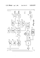
- FIGS. 1-12 represent twelve sheets of LBDs (logic block diagrams) providing detailed circuit schematics of the broadband high-level data link communication line adapter (BHCLA) of the invention.
- BHCLA broadband high-level data link communication line adapter
- FIGS. 1 through 12 is divided into two halves (e.g., FIG. 1a and FIG. 1b) which, arranged in side-by-side fashion with the "a" half on the left, depict one LBD sheet.
- FIG. 1 illustrates the multiline communication processor (MLCP) and data communication equipment (DCE) interface connectors for the BHCLA.
- FIG. 2 generally depicts the LCP address and control decode logic.
- FIG. 3 represents the system and test clock control logic.
- FIG. 4 depicts the MLCP input multiplexer and test multiplexer logic.
- FIG. MLCP multiline communication processor
- DCE data communication equipment
- FIG. 5 illustrates the DCE receivers and driver circuits.
- FIG. 6 shows the transmit FIFO memory and control logic.
- FIG. 7 illustrates the transmit address counter and control memory logic.
- FIG. 8 shows the transmit microprocessor and instruction control logic.
- FIG. 9 illustrates the receive address counter and control memory logic.
- FIG. 10 illustrates the receive microprocessor and associated logic.
- FIG. 11 depicts the receive instruction control logic, and
- FIG. 12 shows the receive FIFO memory and control logic.
- FIG. 13 is a functional block diagram of a system within which the invention may operate.
- FIGS. 14a and 14b when arranged side-by-side with FIG. 14a at the top, provide a schematic block diagram illustrating the BHCLA of the invention.
- FIGS. 15a-15g illustrate the format of various control and status words used with the system of the invention.
- FIG. 15h illustrates the HDLC frame format used for messages handled by the system.
- FIG. 16a is a schematic block diagram of the 4-bit transmit microprocessor used in the system of the invention.
- FIG. 16b shows the receive microprocessor circuit employed in the system, illustrating the manner in which two of the 4-bit microprocessors shown in FIG. 16a are cascaded to provide an 8-bit microprocessor for handling received data.
- FIG. 17a is a block diagram illustrating the basic functions performed by the transmit microprogram set forth in detail in Appendix A.
- FIG. 17b is a block diagram illustrating the basic functions performed by the receive microprogram illustrated in detail in Appendix B.
- FIGS. 18a, 18b, and 18c represent a signal source table wherein every signal employed in the system of the invention is alphabetically listed along with a designation of the circuit element from which the signal emanates.
- Appendix A is a microprogram instruction listing, including applicable instruction and parameter definition information, for the transmit control firmware employed with the communication line adapter of the invention.
- Appendix B is a microprogram instruction listing, including applicable instruction and parameter definition information, for the receive control firmware used with the communication line adapter of the invention.
- FIG. 13 illustrates in functional block diagram form a computer system having a multiline communications processor MLCP 10 in electrical communication with a central processor unit CPU 11 and a main memory unit MEM 12 by way of a common communication bus hereinafter referred to "megabus" 13.
- the megabus 13 provides an information path between any two units in the system.
- the paths are asynchronous in design, thereby enabling units of various speeds to operate efficiently.
- the bus accommodates information transfers including communication requests, control commands, status signals and data transfers between main memory unit 12 and MLCP 10.
- Any system unit requiring communication with any other system unit issues a bus cycle request.
- the bus cycle is granted, the requesting unit becomes the master and the addressed unit becomes the slave.
- Some bus interchanges require a response cycle as well as a request cycle.
- the master unit may identify itself to a slave unit and indicate that a response is required.
- the slave assumes the role of master and initiates a transfer to the requesting unit.
- the CPU 11 has the lowest priority
- the MLCP 10 has the next to the lowest priority
- the memory unit 12 has the highest priority.
- the MLCP 10 further communicates with a broadband high level data link control communication line adapter BHCLA 14 and other communication line adapters 15.
- the BHCLA 14 in turn may be directly connected to data processing equipment such as a CPU, or to any type of data terminal equipment DTE.
- the BHCLA may be connected by way of a local data communications equipment unit DCE 16 and a communications cable 17 to a remote DCE 18 within the data communication network DCN.
- the remote DCE 18 in turn may be connected to remote DTE 19.
- the DCEs have a capacity to both modulate and demodulate binary information streams, and thus may either receive or transmit information.
- the BHCLA 14 may be made compatible with any DCE interface type conforming to the well-known EIA RS-232-C, MIL 18-C or EIA RS-XYZ, CCITT V.35 or BELL 301 or 303 type data sets.
- the preferred embodiment of the invention as described hereinafter is compatible with the BELL 301 or 303 type interface units.
- the BHCLA of the present invention is shown in the schematic block diagram of FIGS. 14a and 14b and in the detailed schematic logic block diagrams of FIGS. 1-12.
- the BHCLA includes a pair of interface connectors 21 and 100 which are coupled, respectively, to the MLCP 10 and to the local DCE 16 (FIG. 13).
- FIG. 14a depicts the transmit circuits of the BHCLA and
- FIG. 14b shows the receive circuits.
- the MLCP exercises control over the system through a set of MLCP address decode and control logic circuits 48 which receive from the MLCP address signals ADDR, control signals CONT, a strobe signal STRB, a master clear signal MCLR, and clock signals SYSCLK and TCLK via interface connector 21. In response to these signals, the logic circuits 48 output a variety of control and timing signals to the remaining circuits of the transmit and receive system to effectate necessary timing and control functions.
- the transmit circuits include a transmit control word register 24 and a transmit extended control word register 22. These registers receive 8-bit and 4-bit control words, respectively, from the MLCP.
- the format of the transmit extended control word is shown in FIG. 15a and the two formats for the transmit control word are shown in FIGS. 15b (start of frame format) and FIG. 15c (end of frame format).
- a transmit FIFO (first-in first-out) buffer memory 26 operates to temporarily store control word data and message data received from the MLCP.
- the operation of the FIFO memory circuits is such that received 8-bit data and control bytes ripple from the input to the output in a rapid fashion such that a queue of data and control bytes is formed. These bytes are transferred via multiplexer 28 to the transmit microprocessor 34 and from there are shifted in bit-serial fashion onto the communication channel via DCE interface connector 100. Control of this operation is effected by control firmware stored in control memory 32.
- An address counter 30 and instruction execution control circuit 36 control the execution of the firmware to carry out appropriate transmit control operations in accordance with the invention.
- the transmitted bit-serial data stream is channeled to connector 100 by a data bit synchronization circuit 40 and a DCE driver circuit 42.
- a transmit clock signal obtained from the DCE is received by receiver circuit 42 and supplied to data bit sync circuit 40 for synchronizing the data stream to the communication channel.
- a cyclic redundancy check (CRC) generator 38 monitors the bit stream and provides CRC check data to the microprocessor 34 for error correction purposes.
- Control information is also provided to the communication channel via the DCE control word register 50, secondary storage register 52, and a 4-bit DCE driver circuits 54.
- An interrupt control circuit 46 operates to feed an interrupt signal TCRIZZ the the MLCP through connector 21 to provide appropriate interrupt and response commands thereto.
- Test mode logic circuits 5 are also provided in the system but do not form an essential function of the present invention and thus are not described further herein.
- the receive circuits of the BHCLA shown in FIG. 14b include DCE receivers 76, 78 and 90 for receiving from the DCE via connector 100 receive clock signals, receive data bit signals, and a 4-bit receive status signal.
- Data bits are transmitted from receiver 78 to data bit sync circuit 74 and from there are transferred to the receive microprocessor 66.
- the latter operates under the control of receiver firmware stored in control memory 70 to assemble the data bits into parallel bytes, to perform CRC error checking via the operation of CRC generator 80 and to perform a variety of additional monitoring, formatting, and controlling functions in accordance with the present invention.
- a receive address counter 68 and instruction execution control circuit 72 operate to provide necessary firmware execution control.
- the MLCP provides control information via a receive control word which is stored in the receive control word register 62 and applied to microprocessor 66 through a multiplexer 64.
- a receive interrupt control circuit 58 operates to provide interrupt and response commands from the receiver circuits to the MCP via interface connector 21.
- Assembled receive data bytes are transferred from microprocessor 66 to a FIFO memory buffer circuit 88 and are thence channeled into the receive FIFO memory circuits 84.
- the latter like the transmit FIFO memory 26, includes a section for message data and a section for status data.
- the FIFO memory 84 also operates to ripple received bytes to the output in rapid fashion to automatically provide a queue of bytes for transfer through multiplexer 82 to the MLCP in the form of LADAT signals on the 8-bit output line 83.
- Multiplexer 82 also operates to enable the MLCP to read the device ID when it first responds to a receiver interrupt command and to read the receive status signal provided by the DCE through receivers 90.
- adapter ready and underrun control signals generated by control circuit 86 are also provided to the MLCP via multiplexer 82.
- a receiver resynchronization circuit 60 operates on command of either the transmit or receive firmware to automatically resync the receiver circuits to the communication channel in anticipation of a data receive operation. This function preconditions the receiver circuits such that the MLCP does not have to respond as quickly to a receive interrupt command.
- the MLCP initializes the system by activating decode logic 48 at the start of a transmit operation.
- the MLCP selects a particular adapter and sets up appropriate registers via the address and control lines coupled to decode logic 48.
- Device ID information is transmitted to the MLCP via multiplexer 82 at the outset to signal the identify of the responding adapter.
- the MLCP transfers DCE control bits to the DCE via DCE control word register 50 to provide an appropriate response to the DCE. Thereafter, the MLCP reads the DCE status through receivers 90 and multiplexer 82 to determine that the DCE is ready to receive transmitted data.
- the MLCP loads control word registers 22 and 24 and then begins transferring data and control bytes to the FIFO memory 26.
- the MLCP continues to load the FIFO memory with transmit data until the memory is full, as indicated by the transmit adapter ready signal TAR generated by circuit 86.
- interrupt control 46 signals the MLCP to cease supplying transmit data.
- the transmit microprogram in control memory 32 operates the transmit circuits to take data and control bytes from the output of FIFO memory 26 and to transmit them to the communication channel.
- the program transmits flag or abort bit sequences as specified by the TIFM bit stored in register 22 (FIG. 15a).
- the program transfers bytes from the FIFO memory into the microprocessor 34 and causes the data to be shifted out of the microprocessor a bit at a time onto the communication channel through the bit sync circuit 40 and driver 44.
- a new set of data and control characters is shifted into the microprocessor from the FIFO memory.
- a transmit byte size counter located in the microprocessor random access memory (RAM) is reloaded with a byte size code developed from the TBS bits in the transmit control word (FIG. 15b) to enable the microprocessor to control the byte size in accordance with the TBS code.
- the program When the program detects a TEOF bit of 1 in the control byte transferred from the FIFO memory (FIG. 15c), it initiates the end of frame transmit sequence.
- the next character transmitted to the channel is known to be the last character of the text field of the frame.
- the first 8-bit half of the CRC check character is transferred from CRC generator 38, complemented and transmitted to the channel. Thereafter the second 8-bit half of the CRC check character is transmitted to complete the FCS field.
- Interrupt control circuit 46 is set to generate an interrupt to the MLCP and the control word registers 22 and 24 are reset.
- the MLCP reads the DCE status through multiplexer 82 and examines the TU bit in the DCE status word (FIG. 15g) to determine if an underrun condition occurred. If TU is reset, no underrun is indicated.
- the MLCP loads a receive control word (FIG. 15d) into register 62 and a resync command issues from decode logic 48 to trigger resync circuit 60 for initializing the receiver hardware. This clears out the FIFO memory circuits and prepares the system for a receive cycle.
- a data bit at receiver 78 is copied into a bit buffer circuit in data bit sync logic 74.
- the receive firmware shifts the data bit into the microprocessor and checks for the presence of a flag sequence 01111110.
- the program looks for the first subsequent non-flag character, which is determined to be the first character of the received message frame.
- the system presets the CRC generator 80 to the all-one state to prepare it for generating the CRC check character and enters a shift register microprogram control sub-routine to being assembling receive characters.
- the receive program enters a data transfer sub-routine whereupon an assembled character is loaded in parallel into the FIFO buffer 88.
- the program then transfers the character into the data section of the FIFO memory 84, resets buffer 88 and loads an all-zero status character from buffer 88 into the status section of the FIFO memory 84.
- Reentry of the shift register microprogram sub-routine assembles the next received character and thereafter reiteration of the data transfer control subroutine loads the character into buffer 88 and thence into the FIFO memory 84 along with an all-zero status byte.
- the program shifts to the flush control subroutine whereupon the last received character is right justified and tested for the partial byte condition.
- the program generates the status word associated with the last character and extracts the byte size and partial byte size information from it to determine the presence of the partial byte condition.
- the accumulated CRC check character is read from the CRC generator 80 eight bits at a time and a remainder check is performed. If the value of the CRC remainder is incorrect, the RFCSE bit of the receive status word is set along with the REOF bit to indicate the FCS error condition and to indicate that the end of the frame has been reached.
- the program then completes the frame sequence by transferring the FCS (as two 8-bit bytes) received from the DCE to the FIFO memory (if the receive control word so specifies).
- a FIFO full indication is present, an overrun condition is indicated.
- the BHCLA processes the rest of the frame, discarding the remaining characters.
- a receive status word is loaded into the FIFO memory including RO and REOF bits in the set state to indicate the overrun and end of frame conditions.
- the receive interrupt control 58 is set to generate an interrupt command to the MLCP.
- the MLCP responds through decode control circuits 48 by reading the receive status and data words through multiplexer 82. Each such read operation shifts the FIFO memory to make the next status and data characters available.
- the MLCP next reads the DCE status via receiver 90 and inspects the output of control circuit 86. If the latter presents an RAR bit in the set state, the MLCP reads another pair of data and status characters from the FIFO memory 84. The MLCP continues with this cycle as long as the RAR bit remains true.
- the MLCP When the REOF bit in the receive status word is set indicating an end of frame condition, the MLCP knows that the last character of the text field of the frame is at the FIFO output. The MLCP reads the last character along with the last status character and inspects the latter to determine if an overrun condition exists or if a frame abort or FCS error condition was detected. Also, the status character is inspected to determine the presence of a partial last byte and the appropriate last byte size. The MLCP then concludes the frame sequence by reading the FCS check character (as two 8-bit bytes) from the FIFO output (if so specified).
- FIGS. 1-12 The logic block diagrams of FIGS. 1-12 are not described herein in exhaustive element-by-element detail in an effort to avoid unnecessarily lengthening and complicating the specification.
- the elements shown in FIGS. 1-12 are referenced to the more general hardware schematic of FIG. 14 through the below-listed cross-reference table setting forth the circuit elements shown in FIG. 14 and giving the corresponding hardware elements illustrated in FIGS. 1-12.
- element reference codes such as, for example, "01B01" and "08B04" are employed to designate the circuit elements.
- the last two digits of such five-digit codes indicate the figure in which the element appears.
- FIG. 14 general schematic diagram is referened to the detailed FIG. 1-12 schematics as follows:
- FIGS. 1-12 where not specifically illustrated by means of a connecting line or lines, are disclosed by the use of signal identifiers such as "CNTRL1-00" as shown at the pin 01 input to connector 01B01 of FIG. 1a.
- the source of this signal, as well as all other signals, can be readily determined by reference to the signal source table provided in FIGS. 18a-18c.
- the signal CNTRL1-00 emanates from element 01B01 (see column 1, line 14 of FIG. 18a).
- FIGS. 1-12 illustrate known, standard integrated circuit logic chips available from commercial IC suppliers.
- the individual part identification code is provided on each element shown.
- JK flip-flop 07D02 (FIG. 2b) is a standard 74LS112 integrated circuit chip.
- Microprocessors 01B08, 01C110 and 07C10 are similar parts 2901 available from Advanced Micro-Devices (A.M.D.).
- the PROMs shown in FIGS. 7b and 9b are available as part Nos. 82S137 from the Signetics Corporation.
- each of the sheets be separated and arranged in side-by-side fashion such that the "a" and "b" halves of each figure can be viewed simultaneously to permit more convenient reference thereto.
- the first micro-program to be described is the transmit program set forth in Appendix A.
- a first column beginning with a $ mark indicates the start of an instruction.
- the INIT001 following the $ is an address tag.
- the address tag is used as a reference in branch instructions.
- the next column which in this case is "MMP" is the instruction itself.
- the third column is reserved for the operand fields of the instruction. In this case, there are five operands beginning with 0# and ending with QR.
- the fourth column beginning with a backslash () mark is the comments field for the instruction
- the fifth, sixth and seventh columns refer to the hexadecimal address of the instruction in the PROM (Programmable Read Only Memory) in the preferred embodiment disclosed herein.
- the sixth and seventh columns refer to the contents in hexadecimal at the indicated address.
- the transmit firmware thus is seen to be 24 -bits wide. More particularly, the contents at hexadecimal address 070000 would be as follows: 0000 followed by 0111 followed by 0000 followed by 0000 followed by 0000 followed by 0000. These correspond to bits specified as bits 00 thru 23, respectively.
- the first instruction MMP (line 19000) is preceded by the word "MICRO". This identifies the instruction as a microinstruction.
- the MMP instruction is an acronym meaning "modify microprocessor"; the MMP instruction effects a change in either the contents of the RAM of the microprocessor used in a transmit operation, or a change in the Q register of the microprocessor.
- the microprocessor used during a transmit operation is a 4-bit microprocessor as shown in FIG. 16a.
- a receive operation two 4-bit microprocessors are cascaded to form an 8-bit microprocessor as shown in FIG. 16b.
- a TAMN instruction is indicated which is an acronym for "test and modify next". The function of this instruction is to test and modify a next sequentially occurring microinstruction. In operation this test instruction performs a test on a function specified by a test field operand, and based upon the results of that test, a next sequentially occurring microinstruction is either executed or ignored.
- an instruction SC refers to a subcommand. This command sets, resets or loads, as indicated by the SC operand field, indicated flip-flops in the hardware of the present invention.
- the instruction BR refers to a branch instruction for branching from a current address to an indicated address to an address specified in the BRADDR operand field.
- the instruction BRSC refers to a branch and subcommand instruction which combines the functions of the SC and the BR instructions.
- the instruction UDSCR refers to the updating of a data set control register.
- the instruction effects the writing of an MLCP signal into a register of the BHCLA.
- the instruction RCRCR refers to a reset of the cyclic redundancy check register.
- the instruction effects the loading of the transmit CRC register with all logic ones.
- the instruction UCRCR indicates an update of the CRC register.
- the next transmit data bit is applied to the CRC register.
- the instruction RER refers to a reading of an external register (i.e., a register external to the microprocessor). Information which has been received from the MLCP thereby is read into the microprocessor.
- the instruction ZERO is merely a tool to set all unused locations in the firmware program to all logic zeroes.
- the WTFLD or word type field distinguishes one instruction from the other for the benefit of the hardware.
- the BR and the BRSC instructions are the same.
- the instruction sets beginning with the MMP instruction through the RER instruction differ as seen by the word type fields.
- the MMP instruction has an operand field (WTFLD/0) indicating that the word type field is set to all logic zeroes.
- the instruction TAMN indicates that the three-bit word type field is set to a 001.
- the word type field is set to a 010.
- the word type field for the instruction RER is set to a 111.
- the word type field is defined at line #2400 of Appendix A wherein it is seen that the field begins with bit 16 and is a 3-bit field. More particularly, bits 16, 17 and 18 of any location in the PROM refers to the word type field. Referring to the LBD of FIG. 8, the decoder 09B08 decodes the bits 16, 17 and 18 to indicate one of the eight instruction types. That is, instructions 0 through 7.
- each of the instructions has two lines of operand fields.
- the first line of operand fields refers to fields which are specified when each instruction is written.
- the second line of operand fields indicates permanently defined operand fields that are not specified where the instruction is written.
- the word type field occurs in the second line of operand fields, and thus is a field which is permanently established and not altered by the program.
- a second operand field in the second line of operand fields is the ISCFLD field which occurs in the case of instructions SC, BR and BRSC.
- the ISCFLD field is an acronym referring to an inhibit of a subcommand.
- This one bit field is a logic zero in the case of a SC or a BRSC instruction which enables the execution of the subcommand. In the BR instruction only, however, the one-bit ISC field is at a logic one level which inhibits the subcommand instruction. Referring to line #2600, it is seen that the ISC field is defined to occur at bit 12 of locations occurring in the PROM.
- the IFWFLD field is an inhibit file write field used in the BR and the BRSC instructions. In each of the instructions, this 2-bit field is set to a logic zero. Referring to the line 2700 of the micro-program, it is seen that the IFWFLD field is a 2-bit field beginning with bit 0. The two bits of the IFWFLD are applied to the microprocessor 01B08 of FIG. 8. More particularly, the bits are applied to pins 6 and 7 of the microprocessor. A logic zero occurring at pins 5, 6 and 7 of the microprocessor 01B08 prohibits the writing of information into the RAM of the microprocessor.
- the KFLD field is a constant field which is used both as an invariable field in the second line of operand fields for the instruction RER, and as a variable field in many of the other instructions such as the MMP instruction.
- the K field provides means for supplying a constant value to the system in order to provide constants for logic or arithmetic functions. Referring to line #2500 of Appendix A, it is seen that the constant field is a 4-bit field beginning with bit 20.
- the K field is in an all logic 1 state.
- the transmit micro-program resides in the six PROMs 01C07, 04C07, 07C07, 10C07, 07D07, 10D07 shown in FIG. 7.
- the mnemonics TUCM00 through TUCM23 refer to the twenty-four outputs of the control memory PROMs 10C07, 07C07, 04C07, 01C07, 10D07, and 07D07.
- the first field to be discussed is the KFLD field, which is referred to as the constant field. This field is used to allow the program to introduce a constant or a mask into the operation. As indicated at location 2500, the KFLD field occurs between bits 20 and 23.
- the four-bit constant field is reflected in the circuit of FIG. 8 by the signals TUCM20, 21, 22, and 23. The signals are reflected in the output of the PROM 07D07.
- the KFLD signals are applied through the wired AND tri-state nodes 07A08, 05A08, 03A08, and 01A08 of FIG. 8 to the data inputs of the microprocessor 01B08.
- the KFLD field is used by the following instructions: MMP, TAMN, SC, UDSCR, RCRCR, UCRCR.
- the FAFLD and FBFLD fields are used to address the internal 64-bit RAM of the microprocessor 01B08.
- the internal RAM is compressed of 16 four-bit words.
- the internal RAM of the microprocessor has two output ports, identified as the A and B output ports as shown in FIG. 16a. In order to address the internal RAM, therefore, two address fields are required. Hence, the FA field and the FB field are identified.
- the FA field and FB field are applied respectively to the A address and B address inputs to the RAM and control the A and B output ports. Referring to lines 3300 through 4900 of the micro-program, it is seen that the FAFLD and FBFLD fields are each four-bit fields.
- the FAFLD field occurs inclusively between bits 12 and 15 while the FBFLD field occurs inclusively between bits 8 and 11.
- the FAFLD field is used with the following instructions: MMP, PAMN, UDSCR, RCRCR, UCRCR.
- the FBFLD field is used with the MMP instruction, USC instruction, the UDSCR instruction, the RCRCR instruction, the UCRCR instruction, and the RAR instruction.
- the OPFLD field is the operation code field referenced at line 5400 of the micro-program.
- the OP field occurs in two different fields, bits 2 through 7, and bit 19.
- the bits in the operation code field specify the arithmetic or logic function to be performed by the microprocessor.
- the logical functions which may be performed by the microprocessor are defined between lines 5600 and 8500 of Appendix A.
- the arithmetic functions are defined between lines 8800 and 12700. Referring to the logic functions, for example line 5900, the logical function A0RB indicates that the data occurring in the input RAM of the microprocessor addressed by the address inputs is logically ORed with the data occurring at the location addressed by the B address inputs of the microprocessor.
- the C indicates that the 062 is an octal value.
- the octal value is applied to bits 2 through 7 and bit 19 as indicated on line 5400.
- the logical functions to be performed are described in the comment field occurring in the third column of the logical functions of the OPFLD field. Such comments also occur in the third column of the arithmetic functions of lines 8800 through 12700.
- D refers to the data on the data input lines of the microprocessor 01B08 of FIG. 8
- Q refers to data stored in the internal Q register of the microprocessor.
- the logic function AND refers to a logical AND
- NOT refers to a logic inversion
- XOR refers to a logic exclusive OR
- XNOR refers to a logical exclusive NOR
- ALUZ indicates that the internal ALU of the microprocessor is forced to an all zero output.
- the P indicates a + or an addition operation
- M indicates a - or a subtraction operation
- 1C indicates a 1's complement
- 2C indicates a 2's complement.
- the function QM1 indicates that a 1 is subtracted from the contents of the Q register of the microprocessor.
- the OPFLD signals occur at the outputs of PROMs 10C07, 07C07, and 10D07 (FIG. 7). These signals are the TUCM02 through TUCM07 signals, and the TUCM19 signal. These signals are applied to the instruction bit inputs 0 through 5 of the microprocessor 01B08, and to the carry-in input CN of the microprocessor.
- the OPFLD field is used in execution of all instructions except the BR, BRSC and 0 instructions.
- the FDFLD field is referred to as the file destination field. Referring to lines 13200 through 13700, it is seen that the FDFLD field is a two-bit field beginning at bit 0.
- the FDFLD fields specifies where the output of the ALU of the microprocessor is stored, and whether a shift is to occur before the data is stored.
- a QR instruction indicates that the data is stored in the Q register of the microprocessor without shift.
- the FR instruction indicates that the ALU output is stored in the internal RAM address specified by the B RAM address input lines of the microprocessor.
- the instruction SRQF indicates that the Q registers shall be shifted right and then stored back in itself, and the output of the ALU is loaded into the internal RAM after being right shifted.
- the SLQF instruction indicates that the information stored in the Q register of the microprocessor is shifted left one bit and then stored in the Q register, and that the ALU output is shifted left one bit and stored into the internal RAM.
- the signal TQRQZZ at the S1 output of the microprocessor refers to the rightmost bit of the Q register.
- the S1 output is connected to the S4 input or leftmost input of the internal RAM of the microprocessor (FIG. 16a).
- the S1 output is applied to the S4 input to the microprocessor, and in a shift left instruction, the S4 output is applied to the S1 input.
- the S1 and S4 terminals are bidirectional pins.
- an eight-bit shift register has been formed by connecting the four-bit Q register with a four-bit location in the internal RAM.
- the output of AND gate 03D08 is applied to the S2 input of the microprocessor.
- a cyclic redundancy check character from the CRC generator 03C08 is shifted into the microprocessor.
- the two bits comprising the FDFLD field correspond to the signals TUCM00 and TUCM01 at the outputs of PROM 10C07 of FIG. 7. These signals are applied to instruction bits 7 and 8 of the microprocessor 01B08.
- This FD FLD field is used by each of the instructions except the BR, BRSC and the 0 instructions.
- the TSTFLD field refers to a test field used only by the TAMN instruction.
- the first column identifies seven hardware functions which may be tested by the TAMN instruction.
- the test field is comprised of four bits, bits 8 through 11 as indicated at line 14400.
- the four-bits correspond to the TUCM08 through TUCM11 signals at the output of the PROM 04C07 (FIG. 7).
- the signals TUCM09 through 11 are applied to the select inputs of the multiplexer 10A08 of FIG. 8.
- the hardware function TRDY is indicated by the occurrence of all logic zeros on the TUCM signals 8 through 11.
- the hardware function indicating that the next transmit bit is ready is tested. If it is found that the bit is not ready, then the next sequential instruction will be executed. If it is found that the next transmit bit is ready, however, the next sequential instruction is treated as a NO OP.
- the hardware function TFMNE is tested when an octal three occurs on the TUCM lines 8 through 11. More particularly, if the transmit FIFO memory is empty, the next sequential instruction is executed. If the transmit FIFO memory is not empty, however, the next sequential instruction is treated as a NO OP.
- the TSTFLD field is used only with the TAMN instruction.
- the SCFLD field refers to the subcommand field used only by the SC instruction of line 19400 of the program.
- the SCFLD field is defined at lines 15900 through 17000 of Appendix A.
- the field is a three-bit field beginning with bit 13, and specifies one of 8 different functions.
- the signals TUCM13 through TUCM15 of the subcommand field appear at the outputs of PROMs 01C07 of FIG. 7, and are applied to the select inputs of the decoder 09C08 of FIG. 8.
- lines 15900 through 17000 of the program it is seen that the occurrence of a hexadecimal 0 on the TUCM13-15 lines indicates the occurrence of a reset transmit bit ready function.
- the occurrence of a hexadecimal one on the TUCM13-15 lines indicates a write transmit bit buffer signal as indicated by the comment field at column three.
- the TUCM signals 13-15 applied to the decoder 09C08 result in one of the outputs of the decoder being lowered to a logic zero level. This occurs during execution of either an SC or a BRSC instruction as identified by the instruction dictionary at lines 18800 through 20800. Note that the SCFLD field is used during the SC, and the BRSC instructions.
- the XRFLD field refers to the external register field which is used only during the execution of the RER instruction as indicated at line 20600 of Appendix A. Referring to line 17700 through 17800, it is indicated that the transfer or XRFLD field specifies one of five different registers to be copied into the microprocessor 01B08 via the data input lines to the micro-processor.
- the XRFLD bit field is specified by the bits 12 through 15 indicated by the TUCM12 through TUCM15 lines at the output of PROM 01C07.
- the TUCM12 signal is applied to the selector inputs of multiplexers 02C06 and 06C06 of FIG. 6.
- the TUCM13-15 signals are applied respectively to AND gates 05D08, 06D08 and 07D08 (FIG. 8).
- the BRADDR field used only by the BR and the BRSC instructions as indicated at lines 19600 and 19800 of the instruction dictionary of the Appendix A, refers to a location to which a branch shall be made. Referring to line 1700 of the program, it is seen that the branch address of BRADDR field is a ten-bit field beginning with bit 2. Referring to FIG. 7, the BRADDR field is characterized by the TUCM02 through TUCM11 signals at the outputs of PROMs 10C07, 07C07 and 04C07. These signals in turn are applied to the four-bit up counters 01A07, 04A07 and 07A07 to address the six PROMs of the program control memory of FIG. 7.
- the format of the receive micro-program is similar to that of the transmit micro-program, and thus only differences between the programs which may be encountered by one of ordinary skill in the art shall be addressed.
- the receive firmware is stored in the PROMs illustrated in FIG. 9, more particularly PROMs 01C09, 04C09, 07C09, 10C09, 04D09, 07D09, and 10D09. It is noted that in the case of the receive firmware, there are seven PROMs as compared to the six PROMs used for the transmit firmware. The additional PROM is required because the receive control word is a 28-bit word rather than a 24-bit word as in the case of the transmit control word.
- the receiver uses two four-bit microprocessors cascaded as shown in FIGS.
- the additional PROM used by the receiver corresponds to the additional four-bits required by the KFLD field used by the receiver.
- the two microprocessors used by the receiver are the microprocessors 01C10 and 07C10 of FIG. 10.
- the receive micro-program is set forth in Appendix B and commences at line 21100 therein.
- the instruction dictionary is located at lines 17500 through 19300 of Appendix B, and the operand fields are defined between locations 1700 and 17000.
- each of the operand fields correspond on a one-to-one basis to the RUCM signals of the receiver.
- the KFLD field defined at line 2500 of Appendix B indicates that the K field is eight bits in length beginning with bit 20 of the receive program control memory. These bits correspond to the signals RUCM 20 through RUCM 27 appearing at the outputs of PROMS 07D09 and 04D09 (FIG. 9).
- RUCM signals are applied through the logic AND nodes 01B10 through 08B10 (FIG. 10) to the data inputs of the microprocessors 01C10 and 07C10. More particularly, the signals RUCM20 through RUCM23 are applied through the logic AND nodes to the data inputs of the microprocessor 01C10, while the signals RUCM24 through RUCM27 are applied to the data inputs of the microprocessor 07C10.
- the FAFLD and FBFLD field signals defined at lines 3300 through 4900 of Appendix B are applied to each of the microprocessors 01C10 and 07C10.
- the FAFLD field signals are applied to the A RAM address inputs of both microprocessors, and the FBFLD field signals are applies to the B RAM address inputs of the microprocessors.
- the OPFLD field signals and the FDFLD signals area applied to each of the microprocessors. More particularly, the OPFLD buit signals corresponding to signals RUCM02 through RUCM07 are applied to the instruction bits 0 through 5 of the microprocessor 01C10, and to the instruction bits 0 through 5 of the microprocessor 07C10.
- the bit 19 of the OPFLD field corresponding to the RUCM 19 signal is applies to the carry-in input CN of the microprocessor 07C10 only.
- the carry-in input of the microprocessor 01C10 is connected to the carry-out output of the microprocessor 07C10.
- the bits 0 and 1 of the FDFLD field are applied to the instruction bits 7 and 8 of each of the microprocessors.
- the TSTFLD field bits and the SCFLD field bits defined at lines 14400 through 17000 of Appendix B will be described subsequently during the description of the operation of the system in connection with FIGS. 1-12.
- the TSTFLD bits 8 through 11 correspond to the RUCM08 through RUCM11 signals applied to the B RAM address inputs of the micro-processor 01C10 and 07C10, and the SCFLD field bits 13 through 15 correspond to the RUCM signals 13 through 15 applied to the A RAM address inputs of the microprocessors.
- the signals RUCM 13-15 are applied to the inputs of a decoder 08C11 (FIG. 11).
- the hardware functions specified by the TSTFLD field are described in the comments field of the third column of Appendix B.
- the SCFLD field may specify one of eight numbers as indicated by the second column. The effect of such a number being applied by the RUCM lines 13-15 is indicated by the commentary field in the third column, where the mnemonic RCX refers to a receiver.
- a further difference between the receive and transmit firmware is indicated in the FDFLD field of the receive program. That is, the SRQF and SLQF instructions are applied differently in the receive microprocessors 01C10 and 07C10. For example, during the execution of the SRQF instruction, the rightmost bit of the Q register of the microprocessor is supplied to the S2 port connected to the leftmost bit of the Q register of the microprocessors 07C10. In addition, the rightmost bit of the internal RAM of the microprocessor 01C10 is applied through the S3 port of the microprocessor to the S4 port of microprocessor 07C10 leading to the leftmost bit of the internal RAM of the microprocessor 07C10.
- a 16-bit shift register thereby is formed comprised of an eight-bit Q register and an 8-bit RAM which is operable for both the left shift and right shift operations.
- a receive data bit is received from the DCE at the S2 port of the microprocessor 01C10 which is shifted into the leftmost bit of the Q register of the micro-processor 01C10.
- the output of NAND gate 04D11 of (FIG. 11) is applied through a logic AND tri-state node 12D10 to the S3 port of the microprocessor 07C10 which is connected to the rightmost bit position of the internal RAM of the microprocessor 07C10. It is thus seen that during a right shift, the S1 and S3 ports of the microprocessor 01C10 are applied to the S2 and S4 ports, respectively of microprocessor 07C10. During the left shift, the S2 and S4 ports of the microprocessor 07C10 are applied respectively to the S1 and S3 ports of the microprocessor 01C10. The S4 port of the microprocessor 01C10 and the S1 port of the microprocessor 07C10 likewise are bidirectional.
- System initialization begins when a master clear signal is received from the MLCP at pin 24 of the connector 01B01 (FIG. 1). The signal thereafter is applied through the inverter 10A02 (FIG. 2) and NOR gates 09B02 and 10B02 to reset registers and flip-flops within the BHCLA.
- the counters 01A07, 04A07, and 07A07 are reset to an all-zero state.
- the counters comprise a ten-bit counter providing address inputs to the transmit control memory comprising PROMS 01C07, 04C07, 07C07, 10C07, 07D07, and 10D07.
- the transmit firmware thereby is initialized and advanced to lines 22300 and 22400 (Appendix A).
- a 238 nanosecond system clock signal is received from the MLCP at pin 18 of the connector 01B01 and applied to inputs of the OR gates 04D03 (FIG. 3).
- the output of the gate 04D03 is applied through the inverter 04C03 throughout the system.
- the system clock is applied to the clock inputs of the counters 01A07, 04A07, and 07A07.
- the counters normally are incremented to address sequential locations in the transmit program control memory.
- TUCM bits 16, 17 and 18 at the output of the PROM 10D07 specify which of eight instruction types are being executed.
- the bits are applied to the decoder 09B08 (FIG. 8) to force a logic zero on one of eight output lines of the decoder.
- the bit 3 output of the decoder 09B08 transitions to a logic zero which is applied to the load inputs of the transmit program counters of FIG. 7.
- the ten-bit branch address specified by signals TUCM02 through TUCM11 thereupon are loaded into the transmit program counters. Referring to line 24500 of the transmit micro-program of Appendix A, it is seen that the microprocessor branches from location hex 010 to location hex 022 rather than to the next sequential instruction indicated by hex 011.
- the transmit program remains in a single program loop as indicated by lines 23100 through 23400 until the MLCP provides initialization information in addition to the master clear signal.
- the master clear signal from the MLCP further is applied to the reset inputs of the counters 01A09, 04A09 and 07A09 (FIG. 9) to reset the counters.
- the counters comprise the receiver program counters for addressing the receiver program control memory comprising PROMs 01C09, 04C09, 07C09, 10C09, 04D09, 07D09, and 10D09.
- the program counters thereupon are set to point to line 21900 of the receive micro-program (Appendix B).
- the RUCM bits 16, 17 and 18 at the output of the PROM 10D09 specify the instruction type being executed. These bits are applied to the decoder 06A11 (FIG. 11) to force one of eight outputs of the decoder to a logic zero level.
- bit 3 output of the decoder is forced to a logic zero level.
- the counters of 01A09, 04A09 and 07A09 thereupon are loaded with the bits indicated by the signals RUCM02 through RUCM11 pointing to a next address in the receiver program control memory. An address other than the next sequential address thereby is provided during a branch type instruction.
- an example branch instruction is shown. From the last three columns, it is seen that a branch is made from the hex location 009 to the hex location 012 rather than the next sequential location 00A.
- the receiver After receiving the master clear signal from the MLCP, the receiver remains in a program loop as indicated at lines 21600 through 21800 until further initialization information is received.
- the MLCP next determines the type of BHCLA to which it is connected. Since the MLCP is connected to a plurality of units other than the BHCLA, the MLCP must supply a particular address to the BHCLA. For example, the ADDRS1 through ADDRS3 signals are applied by the MLCP to the pins 4 through 6 of the connector 01B01.
- the ADDRS3 signal must be a logic zero to address either the transmit address decoder or the receiver address decoder.
- the transmit address decoder is the decoder 01A02 (FIG. 2), while the receiver address decoder is the decoder 04A02.
- the ADDRS2 signal must be at a logic one level and the ADDRS1 signal must be at a logic zero level to address the transmit address decoder. If the ADDRS2 signal is at a logic one and the ADDRS1+10 signal is at a logic 0, however, the receiver address decoder is addressed.
- the MLCP next supplies the control signals indicated by the signals CNTRL1 through CNTRL3 applied respectively to the pins 1 through 3 of the connector 01B01 to indicate the type of function to be performed by the BHCLA. Basically, these control signals indicate which registers are to be loaded or unloaded.
- the control signals are applied to the decoders 01A02 and 04A02. During an MLCP operation, therefore, an output of one of the two decoders transitions to a logic zero level. Since a plurality of devices are connected to the MLCP, the MLCP first must determine what type of device is connected at this address. A logic one on each of the control lines causes the bit 7 output of the decoder to go to a logic zero state. This may occur on either the transmit or the receive decoder.
- OR gate 01D02 When the logic zero occurs at the bit 7 output of either of the two decoders, it is applied to the OR gate 01D02 causing the output of the OR gate to transition to a logic zero state.
- the output of OR gate 02D02 thereupon also transitions to a logic zero level.
- the output of gate 01D02 is applied to the select inputs of the multiplexers 01B04 and 04B04.
- the select input When the select input is at a logic zero, the multiplexers are selected to their "0" inputs.
- the "0" inputs of the multiplexer 01B04 are at a logic one level.
- the four-bit input to the multiplexer 04B04 would be a logic 0110. For other devices, different codes would be wired into the multiplexers to identify the device.
- the output of the gate 02D02 of FIG. 2 is applied to the output enable (F) inputs to the multiplexers 01B04 and 04B04.
- the output enable input of the multiplexer is at a logic zero level
- the aforedescribed codes are applied through the multiplexers to the LADAT0 through LADAT7 lines (line adapter data) through the wired logic and tri-state nodes 01D04 through 08D04 to the connector 01C01 of FIG. 1.
- the signals thereby are supplies to the MLCP to identify the device being addressed.
- the MLCP thereby determines the type of device being addressed, and then may proceed with the initialization process.
- the MLCP next loads the DCE control word register comprised of four-bit registers 08A04 and 11A04.
- the address and control lines of the transmit address and receiver address decoders of (FIG. 2) thereby are set up as described above.
- the bit 5 output of the decoder is transitioned to a logic zero level.
- the output of NOR gate 03B02 is transitioned to a logic 1 level which is applied to the AND gate 03C02.
- the MLCP further supplies a strobe through the pin 25 of connector 01B01 of FIG. 1 and inverter 08A02 to a second input of the AND gate 03C02.
- the output of the AND gate thereupon transitions to a logic zero state which is applied to the clock input of registers 08A04 and 11A04.
- the MLCP supplies DCE control data (FIG. 15f) through pins 17, 18 and 20-25 of connector 01C01 to the data inputs of the registers 08A04 and 11A04. Upon the registers being clocked, the data is loaded into the registers.
- the micro-program as indicated, for example, at Appendix A line 23100 by a UDSCR instruction, clocks register 08B04 to load the contents of the register 08A04.
- the UDSCR instruction causes the bit 4 output of the decoder 09B08 (FIG. 8) to transition to a logic zero. This logic zero is applied to one input of the AND gate 07B04.
- the output of this gate which is responsive to the system clock is applied to the clock input of the register 08B04.
- the output of the register 08B04 supplies control signals to the DCE, the local DCE.
- Such signals are applied to the drivers 01C05, 02C05, 06C05, and 08C05 (FIG. 5), and the outputs of such drivers are applied through the logic elements of FIG. 5 and through the connector 02D01 to the local DCE.
- status information (FIG. 15g) from the local DCE is read by the MCLP through the BHCLA.
- the bit 2 output of either the transmit address decoder 01A02 or the receiver address decoder 04A02 may be transitioned to a logic zero level.
- Such signals are applied to the OR gate 03D02 the output of which transitions to a logic zero to force the output of gate 02D02 to a logic zero.
- the select inputs to the multiplexers 01B04 and 04B04 are at a logic one level to select the multiplexers to their one inputs.
- DCE status information is supplied by the local DCE to the connector 02D01, and through the connector is applied to the DIPS (dual in-line packages) 03A05 through 08A05 (FIG. 5).
- the DCE status information includes the DCERIZ, DCEDSR, DCECTS and DCECDZ signals which are applied through the connector 02D01 to the EIA RS-232-C receiver 01A05, a 24-K pull-up resistor 02A05, and BELL 301 and 303 type interface receivers 06A05 through 08A05, respectively.
- the output of receiver 01A05 is applied through the inverter 01B05 to one input of the multiplexer 01B04 (FIG. 4).
- the outputs of the BELL type receivers 06A05 through 08A05 are applied to the remaining three level one inputs of the multiplexer 01B04.
- the level one inputs to the multiplexer are applied to the line adapter data lines 0-3 which are relayed back to the MLCP as before described.
- the MLCP thereupon examines the DCE status information to determine the operational status of the local DCE. Depending upon the current status of the local DCE, the MLCP initiates transmit and receive operations.
- a transmit operation is initiated when the output of AND gate 12A06 (FIG. 6) transitions to a logic one level.
- the input registers of each of the FIFO memory circuits 01B06, 03B06, 05B06, and 07B06 are empty.
- the output of AND gate 12A06 is applied to an input of AND gate 11C06, thereby causing the output of the gate to transition to a logic one state.
- bit 1 of the DCE control register 08A04 which stores the RTS bit fothe DCE control word (FIG. 15f), must be at the logic 1 level, and that the clear to send signal (FIG.
- the MLCP issues the address and control signals, as before described, to the transmit address decoder 01A02.
- the bit 2 output of the decoder transitions to a logic zero state. It is to be understood that during this period the bit 2 output of the receiver address decoder 04A02 remains in the logic one state, as do all other outputs of address decoders 01A02 and 04A02.
- the output of gate 11C06 also is applied to one input of the gate 03A04.
- the bit 2 output of the decoder 04A02 is at a logic one level which is applied to a second input of the gate.
- the output of the gate 03A04 transitions to a logic zero level which is applied through the inverter 05A04 to a one level input of state 1 of the multiplexer 04B04. Since a device ID is not being read by the MLCP during this time period, the select input to the multiplexer 04B04 is at a logic one level to select the multiplexer to its level one inputs.
- stage one output of multiplexer 04B04 thus is at a logic one level which is applied through the wired AND tri-state node 05D04 to pin 5 of the connector 01C01.
- the MLCP is thereby notified that the input registers of the FIFOs of FIG. 6 are ready to receive transmit control and data information.
- the MLCP thereupon loads the transmit extended control word (FIG. 15a) into the register (FIG. 6). More particularly, the MLCP applies this control data information by way of pins 22-25 of the connector 01C01 of FIG. 1 to the inputs of register 06A06. In addition, the MLCP applies address and control line information to the decoder 01A02 which transitions the bit 1 output of the decoder to a logic zero state and enables the inputs of the register 06A06. The MLCP further applies a strobe by way of pin 25 of the connector 01B01 to the clock input of the register 06A06 to load the register with the control data. It is to be noted that the information in the register 06A06 is used in the transmit operation as further described below.
- the MLCP next supplies address and control information to the decoder 01A02 to transition the bit 0 output of the decoder to a logic zero state which is gated through the AND gate 06B02 by a strobe from the MLCP.
- the MLCP places additional transmit control information on data lines leading to the inputs of the register 01A06.
- the logic zero output of the gate 06B02 is applied to the clock input of the register 01A06 to load the register with a transmit control word (FIG. 15b).
- the outputs of the register 01A06 are applied to the inputs of the FIFOs 01B06 and 03B06.
- the FIFOs 01B06, 03B06, 05B06, and 07B06 form a FIFO transmit buffer which is 16 bits wide and 64 bits deep.
- the FIFOs 01B06 and 03B06 contain transmit control information, while the FIFOs 05B06 and 07B06 contain transmit data.
- the FIFOs 05B06 and 07B06 contain transmit data.
- the loading of the register 01A06 as described above is referred to as the loading of the transmit control word register.
- the operation under which the MLCP loads the register 06A06 is referred to as the loading of the extended control word register.
- the operation regarding the reading of DCE status information (FIG. 15g) is henceforth referred as the status read operation.
- the status read information occurs when the MLCP causes the select input to multiplexers 01B04 and 04B04 to be at a logic one level, and the output enable input of the multiplexers to be at a logic zero level.
- the four DCE status bit signals applied to the level one inputs of the multiplexer 01B04 are applied through the multiplexer to the MLCP by way of the tri-state nodes 01D04 through 04D04.
- the level 1 inputs to the multiplexer 04B04 are applied through the tri-state nodes 05D04 through 08D04 to the MLCP.
- the output of inverter 05A04 is used in both transmit and receive operations, and shall be further described below.
- the next two level one inputs to the multiplexer 04B04 are always at a logic zero state.
- the last level one input to the multiplexer 04B04 is applied by the Q output of the JK flip-flop 06A04, and is used during transmit operations as shall be further described below.
- the loading of a first data character from the MLCP will now be described.
- the MLCP supplies data to the CP data lines leading to the inputs of the FIFOs 05B06 and 07B06.
- the MLCP applies address and control signals to the decoder 01A02 to transition the bit 6 output of the decoder to a logic zero state which is applied through a NAND gate 01B02 to cause the output of inverter 01C02 to transition to a logic zero state.
- the output of gate 01B02 further is applied to the load inputs of the transmit FIFO buffer of FIG. 6, thereby loading transmit data into the FIFOs 05B06 and 07B06.
- the control information previously loaded by the MLCP into the register 01A06 is loaded into the FIFOs 01B06 and 03B06.
- a transmit control word is loaded into the transmit FIFO buffer each time a transmit data word is loaded into the buffer. Since the transmit control word also is stored in the register 01A06, the register need not be refreshed unless the MLCP requires a different control word for a different data word. That is, more than one data word may be used in conjunction with the same control word. Typically, the control word would not be changed until a last character of a transmit data message had been received. In this event, the bit 3 output of the register 01A06 would be set to a logic one level.
- inverter 01C02 (FIG. 2) further is applied to the set input of D-type flip-flop 13A06.
- the set condition of the flip-flop is sensed by the transmit micro-program to indicate that transmit and control information currently is stored in the transmit FIFO buffer. This sensing is accomplished by the TFMNE version of the TAMN instruction as indicated at line 62100 of Appendix A.
- the flip-flop 13A06 is reset by the RSTFMCB version of the SC instruction as exemplified at line 62200 of the transmit program. It is to be noted that when a subcommand is mentioned, it may in fact be combined with the branch instruction as in the case of the BRSC instruction of line 62200.
- the MLCP thence continues to load the data characters into the transmit FIFO buffer of FIG. 6.
- the MLCP is able to load new data into the FIFOs only when the input registers of the FIFOs are empty.
- the MLCP thus repeats the above-described status read operation and then loads a data character.
- the condition of the FIFO input registers being empty is identified by the bit 0 output of the multiplexer 04B04, i.e., the TAR/RAR bit 4 FIG. 15g. That is, if the output is at a logic one level, the FIFO input registers are empty. If it is at logic zero level, however, the MLCP enters a WAIT state awaiting a time when the input registers to the FIFOs will be empty.
- the MLCP enters a WAIT state during a status read operation during which the bit 2 output of the decoder 01A02 is at a logic zero state which is applied to the AND gate 06B02.
- the MLCP sets the control line at pin 20 of the connector 01B01 to a logic zero state which is applied to a second input to the gate 04B02.
- the output of the gate thereby transitions to a logic zero state which is applied through the gate 12C06 to reset the JK flipflop 11D06.
- the output of AND gate 12D06 thereby is forced to a logic one state to inhibit interrupts to the MLCP.
- the MLCP thus enters a WAIT state.
- the transmit firmware program is removing transmit operation words from the transmit FIFO buffer, thereby freeing the input registers of the FIFOs.
- the input register empty output of the FIFOs transitions to a logic one which causes the output of AND 12A06 to transition to a logic one level which is applied through gate 11C06 to cause the flip-flop 11D06 to enter into a set condition.
- the output of gate 12D06 thus transitions to a logic zero level to interrupt the MLCP.
- the MLCP thereby is notified that a next data character may be loaded into the transmit FIFO buffer.
- the MLCP initiates a load control word register operation during which the register 01A06 is loaded with an end-of-frame transmit control word (FIG. 15c) causing the bit 3 output of the register to transition to a logic one state.
- the MLCP then initiates a transmit FIFO buffer load operation in which the end-of-frame control word stored in the register 01A06 is loaded into the FIFOs 01B06 and 03B06, and the last data character of the transmit data message is loaded into the FIFOs 05B06 and 07B06.
- the logic one signal at the bit 3 output of register 01A06 is sensed by the transmit firmware to indicate a last data character being loaded into the transmit FIFO buffer.
- the bit 3 output of register 01A06 is applied as before described through the gate 11C06 to the flip-flop 11D06 to inhibit further interrupts to the MLCP.
- the transmit FIFO buffer of FIG. 6 isolates the operation of the MLCP from that of the transmit control logic.
- the operation of the transmit control logic will now be described. Upon concluding the description of the transmit control logic, a description is given of a final status read by the MLCP to determine whether a message frame was successfully provided to the local DCE.
- the transmit firmware resides in the transmit program control memory comprising the six PROMs 01C07, 04C07, 07C07, 10C07, 07D07, and 10D07 (FIG. 7).
- the PROMs are addressed by the transmit program counter comprising counters 01A07, 04A07 and 07A07.
- the transmit program counter is incremented sequentially by the system clock.
- the transmit program counter may be loaded by information pointing to an address other than a next sequential address within the program.
- the microinstruction control logic comprises the D-type flip-flop 09A08 (FIG. 8), the multiplexer 10A08, the decoder 09B08, and the decoder 09C08.
- the decoder 09B08 the instruction decoder
- the bit 0 through 7 outputs of the decoder correspond to the octal number represented by the three bits in the WTFLD field of the transmit firmware program. Referring by way of example to the locations 19000 through 20800 of the transmit program, more particularly, line 20200 and 20300, it is seen that the three bits of the WTFLD field indicate an octal 5.
- the bit 5 output of the decoder transitions to a logic zero level while the remaining outputs of the decoder 09B08 remain in a logic one level.
- the decoder 09B08 is enabled by the flip-flop 09A08 which is normally in the -- set condition.
- the Q output 8pin 06) of the flip-flop thus is at a logic zero state.
- the flip-flip 09A08 may be reset as a result of the execution of a TAMN instruction. In this event, the -- Q output of the flip-flop 09A08 transitions to a logic one state disabling the decoder 09B08.
- the outputs of the decoder 09B08 all remain in a logic one state.
- the bit 1 output of the decoder 09B08 transitions to a logic zero state which is applied to the enable input of the multiplexer 10A08.
- the bit 1 output of decoder 09B08 is at a logic one level.
- the D1 output of the multiplexer (pin 06) thus is at a logic one level which causes the flip-flop 09A08 to remain in a set condition.
- the Q output of the flip-flop thus is at a logic zero level and the next occurring firmware instruction is executed in the normal manner.
- the enable input to the multiplexer 10A08 is at a logic zero level.
- the multiplexer input selected by the select inputs to the multiplexer 10A08 may cause the D1 output of the multiplexer to transition to a logic zero level.
- the logic zero state causes the flip-flop 09A08 to be reset.
- the Q output of the flip-flop thereupon transitions to a logic one level to cause the next instruction in the transmit firmware program to be ignored.
- the decoder 09C08 is a subcommand decoder which generates subcommands.
- the bit 2 output (pin 13) of the decoder 09B08 transitions to a logic zero level.
- the bit 3 output of the decoder transitions to a logic zero level.
- the bit two and bit 3 outputs of the decoder are applied to the gate 11C08, the output of which is applied to one enable input of the decoder 09C08.
- the output of the gate 11C08 transitions to a logic zero level. If the bit 3 output of the PROM 01C07 (FIG.
- the decoder 09C08 is at a logic zero level also, one of 8 outputs of the decoder 09C08 transitions to a logic zero level as indicated by the three inputs to the decoder.
- the three inputs to the decoder 09C08 correspond with the three bits comprising the SCFLD field of the transmit firmware program as defined at lines 15900 through 17000.
- an octal code of three is applied to the input of the decoder 09C08, and the bit 8 of the decoder transitions to a logic zero level.
- the transmit microprocessor consists basically of three parts, namely a 16 word by 4-bit RAM, a Q register and an arithmetic and logical unit (ALU).
- the RAM is used for the temporary storage of transmit data, transmit control information and transmit status.
- the Q register is used for the temporary storage of miscellaneous control information. Arithmetic and logical operations are performed by the ALU.
- a left/right shifter including registers 120 and 122 is also provided so that the results of the ALU operations may be shifted either left or right before being stored back into the RAM or in the Q register.
- the microprocessor is able to execute a number of different instruction types as determined by the data from the PROMS of FIG. 7 as applied to the nine instruction input lines of the microprocessor.
- Eight address lines from the transmit control program memory PROMS (FIG. 7) are applied to the A RAM address lines and the B RAM address lines of the microprocessor (FIG. 8) to specify the A and B port address of the RAM.
- Data into the processor is supplied from any of the following six sources: control memory 07D07, register 06A06, and the four FIFO memories 0B06, 03B06, 05B06, and 07B06 by means of the two selectors (multiplexers) 02C06 and 06C06. The process for reading data in each of these sources is further described below. It is noted that the data are provided to the micro-processor by means of the four wired AND circuits 01A08 through 07A08.
- the microprocessor 01B08 has two outputs in addition to the shift outputs which were described above. The first of these outputs is data output bit 1 which is connected to flip-flop 02C08. The second output is the transmit ALU equals 0 output which is applied to the "6" input of multiplexer 10A08 and the inverter 13A08. The output of inverter 13A08 is applied to the "7" inputs of MUX 10A08.
- This connection to the multiplexer 10A08 which is the instruction TAMN multiplexer, provide a means for the microprogram to test the results of any operation within the microprocessor 01B08.
- An example of the ALUEZ version of the TAMN instruction is shown at line 35900 of Appendix A.
- the contents of RAM location E are logically ANDed with the program supplied hexadecimal constant 1. If the result of this operation is 0, then the branch instruction at line 36000 will be executed. If the result of the operation is not a 0, then the branch instruction at 36000 is ignored and the next meaningful instruction would be the MMP instruction at line 36100.
- An example of the ALUEZ version of the TAMN instruction is shown at line 36500.
- the contents of RAM location 4 are subtracted from the data on the data input lines to the microprocessor 01B08 which in this case is a constant of value hexadecimal C. If the result of this operation is a non-zero value, the instruction at line 36600 will be executed in the normal manner. If the result of the operation does equal 0, however, the instruction at line 36600 will be ignored and the next instruction that will be executed will be the instruction on line 36800.
- the transmit microprogram is responsible for sending data on a bit-by-bit basis to the local DCE.
- the first type of data is the flag or abort sequences which are transmitted between frames, which are also known as interframe time fill.
- a flag sequence is defined as a 0 bit followed by six 1 bits, followed by a 0 bit, i.e. a hexadecimal 7E.
- An abort sequence is defined as seven or more 1 bits, i.e. a hexadecimal FF.
- the second type of data is the start of frame flag, which is automatically generated by the transmit microprogram before sending the first data character of each frame.
- the third type of data is the data characters of the frame all of which are provided by the MLCP via FIFOs 05B06 and 07B06.
- the fourth type of data is the FCS data, which is generated by the transmit program by using the CRC register 03C08. This error-checking sequence is calculated using each data bit of the frame provided by the MLCP and is transmitted at the end of the frame after the last character provided by the MLCP has been transmitted.
- the fifth type of data is the closing or end-of-frame flag that is automatically generated by the transmit program and sent after the FCS has been transmitted.
- the sixth type of data that is sent is the abort sequence which is automatically generated and sent by the transmit program whenever an underrun situation occurs.
- a new transmit data bit is sent to the local DCE at each transmit bit boundary, i.e. at each positive-going edge of the transmit clock from the local DCE, in the following manner.
- the transmit clock is received from the local DCE at pin 02 of connector 02D01 (FIG. 1).
- This signal is applied to input receiver 03A05.
- the output of this receiver is applied to the input of receiver 03B05.
- the output of receiver 03B05 is applied to the input of multiplexer 11C04 (FIG. 4). More particularly, it is applied to the zero input of circuit 1 of this multiplexer.
- the output (pin 04) of circuit 1 of this multiplexer is applied to flip-flops 01D08 and 02D08.
- next transmit data bit is thereby shifted from flip-flop 02C08 as described below, and that the Q output (pin 09) of this flip-flop is applied to the data input of flip-flop 02D08, it is seen that the next transmit data bit is thereby shifted from flip-flop 02C08 into flip-flop 02D08 on the positive-going edge of the transmit clock signal.
- the Q output of 02D08 is applied to the input of driver 04C05 (FIG. 5).
- the output of this driver is connected to zener diode 04D05 and the output of the zener diode is connected to pin 6 of connector 02D01.
- the transmit data is provided to the local DCE.
- the transmit clock signal is also applied to the clock input of flip-flop 01D08. Since a pull-up resistor, which is a logic one level, is applied to the data input of this flip-flop, the Q output (pin 09) of this flip-flop goes to the logic one state with each positive-going transition of the transmit clock.
- This set condition of 01D08 is used to indicate to the transmit program that the previous transmit data bit has been shifted out of flip-flop 02C08 and into flip-flop 02D08, and therefore that it is time for the transmit program to load the next transmit data bit into flip-flop 02C08.
- the transmit program monitors flip-flop 01D08 by means of the TRDY version of the TAMN instruction as shown, for example, at line 29900 of the transmit program (Appendix A).
- the transmit microprogram Upon the detection of the set condition of the ready flip-flop 01D08, the transmit microprogram resets this flip-flop by means of the RSTRDY version of the SC or BRSC instruction as shown for example at line 30300. After resetting the transmit ready flip-flop in this manner, the transmit program provides the next bit of transmit data to flip-flop 02C08 as discussed below.
- a new transmit data bit must be loaded into flip-flop 02C08. This is accomplished by means of the WRTBB version of the SC instruction such as shown, for example, at line 35600 of the transmit program.
- the next transmit data bit which is stored in the rightmost bit position of RAM location E, is applied to data out bit 1 of the microprocessor 01B08. This bit is in turn applied to the data input of data flip-flop 02C08.
- This particular SC instruction causes the one output of decoder 09C08 to transition to the logic zero state and then back to the logic one state.
- This signal is applied to the clock input of the transmit bit buffer flip-flop 02C08, and causes the next transmit data bit to be stored in this flip-flop upon execution of this instruction.
- This operation whereby a new transmit data bit is loaded into flip-flop 02C08 is hereafter referred to as the loading of the transmit bit buffer.
- the transmit microprogram While waiting for the MLCP to provide transmit data for the frame, the transmit microprogram generates and sends fill characters of either flag or abort sequences. This is done one bit at a time by loading the appropriate data bit into flip-flop 02C08 at each bit boundary as explained above. Whether flags or aborts are sent is determined by the MLCP, and is explained further below.
- each byte is controlled by a 4-byte counter stored within one of the 60 RAM locations of the transmit microprocessor 01B08.
- This counter is initially loaded to a count of eight by an MMP instruction which copies the constant field bits of the control memory 07D07 (FIG. 7) through the wired AND circuits 01A08 through 07 08 to the data inputs of the microprocessor. See line 52800, for example, of the Appendix A transmit microprogram.
- this counter is decremented by one (e.g. line 50900), and tested by the ALUEZ version of the TAMN instruction to see if a value of zero has been reached indicating that a transmit byte boundary has occurred (e.g. line 51000).
- the occurrence of the all-zero condition is hereafter referred to as a transmit byte boundary.
- the microprogram must generate and store the next flag or abort fill character, which will be shifted into the transmit bit buffer flip-flop 02C08 on the next 8 subsequent bit times. Whether a flag or an abort is to be generated is specified by bit 3 of the 4-bit extended transmit control word stored in register 06A06. The contents of this register are read into the transmit microprocessor 01B08 by means of the TXCW version of the RER instruction (e.g. line 65600). When an RER instruction is executed, the seven outputs of decoder 09B08 transition to the logic zero level which is applied to one input of gate 05D08.
- the output of PROM 01C07 which is applied to gate 05D08 is also at the logic zero level.
- the output of gate 05D08 is attached to the output enable inputs F of register 06A06.
- the resulting logic zero level of this signal enables the output of register 06A06.
- These outputs are attached to the four wired AND functions 01A08 through 07A08 which in turn connect to the data input port of the microprocessor 01B08. In this manner, the control word previously provided by the MLCP is loaded into the transmit microprocessor for further use.
- the TIFM bit (bit 3-FIG. 15a) is examined to determine whether a flag or an abort sequence is to be generated.
- the bit is tested by the TAMN instruction (e.g. line 65700).
- a flag or an abort is then generated as shown in line 65900 through 66600, and stored in a location of the microprocessor internal RAM.
- the flag or abort sequence thus generated is sent out bit-by-bit on the succeeding bit boundaries (e.g. line 50800).
- the register of the RAM is shifted right one bit position as exemplified by lines 51600 through 51800 of the transmit program.
- the transmit program checks to see if the previous interrupt has been completed. This is accomplished by means of the TCRI version of the TAMN instruction as exemplified at line 60900 of Appendix A. This instruction provides a means for testing the transmit interrupt flip-flop 11D06 (FIG. 6). If the previous interrupt has in fact been completed, then the instruction following this TAMN instruction will be executed (e.g., line 61000). If the previous interrupt has not been completed, then the following instructions would be ignored and the second-following instruction will be executed instead (e.g. line 61100).
- the MLCP has loaded a 1 bit into bit position three (pin 09) of register 01A06 which, after being inverted by gate 04A06, becomes a logic zero at the input to gate 11C06 of FIG. 6 and hence holds the output of this gate at the logic zero state thus preventing the interrupt flip-flop 11D06 from setting.
- the transmit program finds that the previous interrupt has been completed, the transmit program executes the RSTFMCB version of the SC instruction (e.g. line 61900). Execution of this intruction causes the bit 5 output of decoder 09B08 to transition to the logic zero level. This signal is applied to the reset input of the above-mentioned register 01A06 and resets the entire register to the logic 0 state.
- the transmit program tests the transmit FIFO buffer memory to see if control information for data for a frame has been provided.
- the full outputs of each of the four FIFOs 01B06 through 07B06 are at the logic one level and are applied to gate 11A06.
- the output of this gate is at the logic one level when the output register of the FIFO has data in it. This is tested by the transmit program by means of the TFMOR version of the TAMN instruction (e.g., line 53900 of Appendix A). If the output register is not ready, an additional flag or abort sequence is generated and transmitted as discussed above.
- the microprogram When the transmit FIFO memory of FIG. 6 is found to have data available, the microprogram reads the control information and transmit data into the internal RAM of the transmit microprocessor. Since the data path of the transmit control logic is only 4 bits wide, the loading of the 16-bit transmit data and control information requires four separate instructions. Four versions of the RER instruction are used, namely, the TCWL, TCWR, TDL, and TDR versions (e.g., lines 58400 through 58700 of the transmit program).
- the control word that is when either a TCWL or TCWR instruction is being executed
- the output of gate 06D08 is connected to the output enable input of MUX 02C06 of FIG. 6, is at the logic zero level, thus enabling data from either FIFO 01B06 or 03B06 to be loaded into the transmit microprocessor 01B08 via the four wired AND circuits 01A08, 03A08, 05A08, and 07A08.
- the select input to MUX 02C06 is at the logic zero level, thus selecting the bit zero inputs which are connected to the left-half of the control word, namely FIFO 01B06.
- the select input to MUX 02C06 is at the logic one level, thus enabling the bit 1 inputs, which are attached to the FIFO 03B06.
- the output of gate 07D08 which is attached to selector 06C06, is at the logic zero level, thus transferring the data in either FIFO 05B06 or 07B06 to the transmit microprocessor.
- the select input to MUX 06C06 is at the logic zero state, thus selecting the bit 0 inputs which are attached to FIFO 05B06.
- the select input to MUX 06C06 is at the logic one level, and the bit 1 inputs from FIFO 07B06 are enabled.
- an output strobe must be issued to the transmit FIFO in order to reset the output registers, and allow the next data and control words to advance into the output registers. This is accomplished by means of the RSTFMOR version of the SC instruction, (e.g., line 58800).
- the "2" output of decoder 09B08 and the "6" output of decoder 09C08 both transition to the logic zero state thus setting flip-flop 09D08.
- the Q output (pin 05) of this flip-flop which is applied to the four transmit FIFOs buffers, transitions to the logic one level and resets the output registers of the four FIFOs. This flip-flop will be reset as soon as another instruction is executed. After this operation, new transmit data and control information can advance to the output registers of the FIFOs.
- the transmit program uses the TAMN instruction to examine the control word associated with each transmit data character.
- the TEOF bit (bit 3-FIG. 15c) is the end-of-frame control bit, and is always found reset until the MLCP has provided the last character of the frame.
- Other bits in the control word are used to specify the format of the frame.
- the parameters that are specified include whether or not the frame (FIG. 15h) contains an extended address field, an extended control field, a logical control field, or a test control byte.
- three bits specify the byte-size of the test field portion of the frame.
- the transmit control program After the transmit control program has detected the presence of the first character of a frame, it generates and transmits an opening flag sequence before transmitting this first character. It also initializes the transmit CRC of the SC instruction (e.g., line 59400 of the Appendix A). Execution of this instruction causes the bit 7 output of decoder 09C08 which is attached to the set input of CRC generator 03C08, to transition to the logic zero state which presets the CRC generator to the all-ones condition.
- the transmit CRC of the SC instruction e.g., line 59400 of the Appendix A
- each bit between the opening and closing flag is applied to the CRC register by means of the UDSCR instruction (e.g, line 36600).
- UDSCR instruction e.g, line 36600
- output 5 of decoder 09B08 remains at the logic one level but output 6 (pin 09) transitions to the logic zero level.
- These signals are applied through gate 07B08 to gate 07C08 and to the enable input of the CRC generator.
- the system clock input to gate 07C08 causes a logic one to occur on its output which is applied to the clock input of the CRC generator. Noting that the output of the data bit buffer flip-flop 02C08 is attached to the data input of the CRC generator, and because the enable input is at the logic one state as mentioned above, the clock input causes the new transmit data bit to be shifted into the CRC generator.
- the transmit program monitors the data stream as it is sent to the local DCE, and generates and inserts a zero data bit any time a string of five contiguous one bits occurs, as required by the HDLC protocol. Refer to lines 35900 through 36100 and 36700 through 37500 of the Appendix A program.
- the transmit program After the transmit program has finished sending the opening flag of the frame, it sends the first data character that was obtained from the transmit FIFO as described above. After this first data character has been transmitted, the program again checks the FIFO output register by means of the TFMOR version of the TAMN instruction to determine if another character is available. Assuming that it is, the program then reads the control word and the data character into the RAM of the transmit microprocessor as described above. Assuming that bit 3 (TEOF) of the control word, the end-of-frame indicator bit, is not set, the transmit program sends out a second character in the same manner as described above. This process is then repeated for each character of the frame.
- TFMOR version of the TAMN instruction the program again checks the FIFO output register by means of the TFMOR version of the TAMN instruction to determine if another character is available. Assuming that it is, the program then reads the control word and the data character into the RAM of the transmit microprocessor as described above. Assuming that bit 3 (
- the program executes a STUNDRN version of the SC instruction which causes the transmit underrun flip-flop 06A04 (FIG. 4) to enter the set condition, (e.g., line 129600). Later, when the MLCP reads the final status at end of frame, it will be notified of the underrun condition by means of the TUNDRN signal applied to the fourth bit of multiplexer 04B04 by flip-flop 06A04. Meanwhile, the transmit control program generates a single abort sequence and transmits it bit by bit to the local DCE.
- a frame thus aborted notifies the remote DTE of the error condition at the sending DTE.
- the transmit program continues to generate and send flag sequences while waiting for an end-of-frame condition to occur and for all previous interrupts to the MLCP to be completed.
- This feature of the BHCLA of sending one abort sequence only, then followed by flag sequences is an important function because it properly aborts the message but does not place the transmit line in the vital state. Note that this is performed entirely by the BHCLA transmit logic without requiring any interaction from the already overloaded MLCP.
- Each character of the frame is taken from the FIFO by the transmit program and serially shifted bit by bit to the local DCE as described above.
- Each character is monitored as required, primarily for purposes of byte-size control of the text field portion of the message. For example, if the frame contains a test control byte TCB (FIG. 15h), then the program will monitor the frame first through the address field bytes, and then through the control field bytes. Then upon receipt of the test control byte, the byte-size information is extracted from this byte and stored within a location of the microprocessor RAM.
- TCB test control byte
- the program then monitors the logical control field LCF, if applicable, and then, upon receipt of the first text control byte of the frame, switches byte sizes from 8-bits (which applies to the address, control, test control byte, and logical control field portions of the frame) to the byte-size specified by the test control byte. This procedure is repeated as long as the end of frame indicator bit of the control word is found to be in the reset condition.
- the MLCP can specify further format changes through use of the transmit control word (FIG. 15b).
- the TCFX bit (bit 0) of the control word when in the set (1) state, indicates the presence in the frame of an extended control field.
- the TAFX bit (bit 1) when set, indicates the presence of an extended address field.
- the TTCB bit (bit 2) when set, indicates the presence in the frame of a text control byte TCB (FIG. 15h) and the TLCF bit (bit 7), when set, indicates the presence of the logical control field LCF.
- the TBS bits (bits 4, 5, and 6) specify the byte size of the text field portion of the frame.
- the TEOF (bit 3) is normally reset and is set to denote the last character of the frame.
- the MLCP can specify a "bit stream mode" of operation by entering the code 011 in the TBS control word bit positions.
- This mode of operation provides for the transmission of data from, say, one computer memory to another computer memory, where the data does not follow any particular character structure (e.g., as during a program or memory dump). In this situation it is desirous to send the eight-bit data bytes high-order, or rightmost bit first.
- bit stream mode is specified, either directly by the MLCP through the transmit control word, or indirectly by the contents of the text control byte in the data stream itself, the transmit control program "flips" each character before transmitting it to the local DCE. This is done by the instructions shown at lines 88600-91600 of the Appendix A microprogram listing.
- a further feature of significance involving the use of MCLP-supplied control words lies in the use of the TBFM bit in the extended control word (FIG. 15a).
- the program sends an opening flag and then begins transmission of the frame. This is not always desirable because now the MLCP must continue to supply characters at a rapid rate to keep pace with the high speed transmission line or suffer the occurrence of an underrun error.
- the MLCP sets the TBFM bit in the extruded control word stored in register 06A06
- transmit program senses this condition and sends flag sequences but does not remove and send any actual data from the FIFO.
- This mode of operation continues as long as the TBFM bit is set.
- the MLCP can then load up to sixty-four characters into the FIFO buffer at a pace suited to its prevailing situation. That is, when the MLCP has other operations to perform and is not solely dedicated to the BHCLA, it may load the transmit FIFO as a low-priority function without having to be concerned about underrun. Conversely, when the MLCP can accommodate the high data transfer rate, it resets the TBFM bit to allow the program to start transmission of the frame immediately.
- the last data character of the message is present.
- the first step in ending a frame is the transmission of the last data character.
- the transmission of this character is similar to the transmission of all previous characters except that this byte may be a partial byte as indicated by the TPLB control bit and the character size of this byte may be any size from one bit through 8 bits as determined by TLBS bits 4, 5, and 6 of the end-of-fram control word.
- the next step at end-of-frame is the transmission of the 16-bit CRC sequence which was calculated for the frame, and now is residing within the CRC generator 03C08.
- the first 8 CRC bits are read into the microprocessor one bit at a time, complemented, stored in the internal RAM of the microprocessor, and then shifted out one bit at a time to the local DCE in the same manner as the other transmit data characters. This process is then repeated for the remaining eight bits of the CRC register.
- the actual reading of the CRC register into the transmit microprocessor is accomplished by means of the RCRCR instruction as shown at lines 114200 through 115000 of the Appendix A transmit program.
- This instruction is similar to the UCRCR instruction previously described except that in this case the bit 5 output of decoder 09B08, which is applied to the enable input of the CRC generator 03C08, transitions to the logic 0 state, which allows the calculated CRC sequence to be shifted out instead of causing a new calculation to be performed.
- a closing flag sequence is generated, stored and shifted out one bit at a time by the transmit control program. Then a final interrupt is generated to the MLCP as described below.
- the paragraph above describes the normal end-of-frame operation.
- the transmit control logic provides for a number of variations and additions to this normal procedure. These variations are selected by the MLCP and specified to the transmit control logic by means of the transmit control word associated with the last transmit data character, FIG. 15c. That is, after the program has read the last data character and associated control word from the transmit FIFO buffer memory, it examines these bits to see if a special operation is required. First, the TNFCS control bit specifies whether or not the calculated CRC sequence should be sent. That is, the user may wish to generate his own checking sequence, in which case it can be provided to the transmit control logic as part of the transmit data stream.
- the user may wish to end the frame with an abort sequence instead of with a flag sequence in order to provide the frame abort procedure. This is effected when the TA bit is set to the 1 state.
- a method is provided such so that the receive logic may be issued a resynchronization command from the transmitter as soon as the transmitter completes transmission of the frame. This is effected when the TRR control bit is set to the 1 state. This allows the user to resynchronize the receiver as soon as the transmitter has completed the transmission of the frame in anticipation of a message being sent back to the receiver from the remote DTE transmitter. This receiver resynchronization is accomplished by means of the SRCRSYN version of the SC instruction as shown for example at line 118900 of the Appendix A transmit program.
- the transmit program At the end of the frame the transmit program generates an interrupt to the MLCP. This is accomplished by means of the STCRI version of the SC instruction (e.g., line 132700). Execution of this instruction causes the bit 3 output of decoder 09C08, which is applied to the set input of flip-flop 11D06, to transition to the logic 0 level momentarily, and thus to put this flip-flop in the set condition and hence generate a transmit interrupt as previously described. Note that the interrupt is generated, that is, flip-flop 11D06 is set, even if not all of the inputs to gate 11C06 are at the logic one level. More particularly, even if clear-to-send from the local DCE has gone to the off condition, the interrupt will still be generated. In response to this interrupt, the MLCP reads the DCE status in the manner previously described.
- the MLCP examines the bit 4 output (pin 12) of multiplexer 04B04 which is applied through wired AND node 08D04 to pin 9 of connector 01C01, which reflects the condition of the underrun flip-flop 06A04 at this time in order to determine whether the frame was transmitted properly or if an underrun error condition occured. Now the MLCP performs a transmit WAIT operation which causes the output of gate 12C06, which is attached to both the interrupt flip-flop 11D06 and to the underrun flip-flop 06A04, to transition to the logic zero state and thus reset these two flip-flops. This then removes the interrupt condition from the MLCP.
- the transmit control program is now in the interframe condition again. As has been previously discussed, in this condition, flags or abort sequences are transmitted while waiting for the MLCP to provide the first data character of a new frame.
- An interrupt is normally generated to the MLCP at each byte boundary. If the MLCP wishes to terminate transmit operations rather than to send another frame, these interrupts generated at each byte interval may be used as a timer. More particularly, the MLCP would wait for three such interrupts, for example, before resetting the request to send control line to the local DCE. This would insure that the message just transmitted was completely received by the receiver at the remote DTE.
- the receive operation beings when the MLCP loads a receive control word (FIG. 15d) into registers 01A10 and 05A10 (FIG. 10). This pair of registers is hereafter referred to as the receive control word register.
- the MLCP In loading this register the MLCP first puts the applicable control information on the eight CPDAT lines. The MLCP then sets up the six address and control lines to the receive address decoder 04A02 to cause the bit 1 output thereof, which is applied to an enable input of the receive control word register, to transition to the logic zero level. The MLCP next issues a strobe signal which is applied to the clock inputs of the receive control word register and thereby loads the control information on the input data lines into the control word register.
- the MLCP now initializes the receive control logic by performing what is defined as a receive resynchronization operation.
- the MLCP sets up the six address and control lines to the receiver address decoder 04A02 to cause the bit 4 output, which is applied to gate 07B02, to transition to the logic zero level.
- the output of this gate is applied to an input of gate 07C02.
- the MLCP then issues a strobe signal which is applied to a second input of gate 07C02 and causes a positive going pulse to occur on the output of that gate. That signal is in turn applied to flip-flop 07D02 and causes it to set.
- the output of this flip-flop is sensed by the receive control logic as described below.
- This resychronization operation can be performed at any time, and it can also be performed in a similar manner by the MLCP through the transmit address decoder 01A02.
- This control logic consists basically of four parts, namely the program address counter, the program control memory, the instruction execution logic, and the microprocessor pair.
- the receive program address counters comprise counter register 01A09, 04A09, and 07A09, and their operation has been previously described.
- the receive control memory comprises PROMs 01C09, 04C09, 07C09, 10C09, 04D09, 07D09, and 10D09, and their functionality has also been described previously.
- the instruction execution logic comprises the basic instruction decoder 06A11 (FIG. 11), the subcommand generator decoder 08C11, and the test and modify next (TAMN) multiplexer 09A11, and flip-flop 08A11. Each of these functions has been partially described previously.
- the eight bit receive microprocessor circuitry which comprises four-bit microprocessor 01C10 and four-bit microprocessor 07C10, have likewise been previously described. More particularly, first the transmit microprocessor was described, and then the receive microprocessor was described with reference to its similarities and differences to the transmit microprocessor.
- An eight-bit data byte is provided to the eight data input lines of the microprocessor pair via the wired-AND nodes 01B10 through 08B10 from the receive control word registers 01A10 and 05A10 during AR instructions, and from PROMs 04D09 and 07D09 during all other instructions.
- the eight data output lines of the receive microprocessor paid are applied to the receive FIFO memory buffer 04A12, where receive data and receive status bytes are temporarily stored before being loaded into the appropriate portion of the receive FIFO memories of FIG. 12a.
- the high order bit of microprocessor 01C10 that is, data bit 0, is also applied to the data input pin of the receive CRC generator circuit 04C11.
- the ALU operation result output from each of the two four-bit microprocessors is wired-ANDed at node 06D10 and are then applied to the TAMN multiplexer 09A11. This signal is also applied to the inverter gate 13A11, whose output is applied to another input of the TAMN multiplexer.
- the receive control program monitors the receive resynchronization flip-flop 07D02 (FIG. 2), which may be set by either the MLCP directly or by the transmit control program as described above, to see if a resynchronization command has been received. Testing of this flip-flop is accomplished by means of the RCRSYN version of the TAMN instruction, such as exemplified at line 27800 of Appendix B. If the flip-flop is reset, the branch at line 27900 is ignored, and the program continues on to the instruction at line 28200. If set however, the branch at 27900 is executed, and the program continues at line 30000. Here the necessary internal initialization for synchronization is performed, and an RSRCRSYN subcommand instruction is executed to reset the resynchronization flip-flop (e.g., see line 31700 of Appendix B).
- flip-flop 02C11 the next receive data bit mentioned above is thus loaded into this flip-flop.
- this flip-flop is set to indicate the presence of a new receive data bit in flip-flop 02C11.
- the program senses this condition by means of the RRDY version of the test instruction as shown at Appendix B line 26700.
- the program resets this flip-flop by means of the RSRRDY subcommand instruction at line 27100.
- the subcommand instruction may be combined with the branch instruction to form a BRSC instruction as shown at this line 271001.
- the receive control program next shifts the data bit into the microprocessor. This is accomplished by the SRQF version of the MMP instruction (line 37000).
- the input to inverter 03B11 is at a logic zero level and hence the output, which is applied to AND gate 03C11, is at a logic one.
- the other input to gate 03C11 is also at a logic one at this time, and the output, which is applied to gate 02D11, is at a logic one.
- the output of flip-flop 02C11, which is coupled to the other input of gate 02D11, is now enabled throught this gate and applied to the left shift input of the Q register of microprocessor 01C10 (FIGS. 10b and 16b).
- the current data bit is shifted into the Q register of the receive microprocessor pair. More particularly, the right shift operation is performed because the bit three output of PROM 10C09 at pin 1 is at a logic one level, and the bit two output at PROM pin 12 is at a logic zero level, the right shift operation is executed. In this manner each new receive data bit is shifted into the receive microprocessor. This is hereafter referred to as an input next receive data bit operation.
- each data bit is shifted into the microprocessor as described above.
- Each new bit is stored along with the previous seven bits in a location within the internal RAM of the microprocessor.
- These eight bits are examined each bit time to see if they comprise a flag sequence, 01111110 (Appendix B line 39900). Detection of a flag sequence indicates that character synchronization has been achieved.
- This flag sequence and any additional flag sequences are discarded by the receive program while searching for the first non-flag, non-abort (11111111) character. The first such character found is the first character of a frame.
- the control program reads the receive control word registers 01A10 and 05A10 at various times to determine the format of the frame as specified by the MLCP. This inputting is accomplished by the RER instruction (e.g., line 73900). Execution of this instruction causes the bit 7 output of instruction decoder 06A11 to transition to the logic zero level. This signal is applied to an input of inverter 09B11, whose output is supplied to PROMs 04D09 and 07D09. The resulting logic level 1 at the enable inputs of these PROMs forces their outputs to the high impedance state. Note that during the execution of all other instructions, the outputs of these PROMs, which contain the constant field of the instruction, are enabled.
- the bit 7 output of decoder 06A11 which is at the logic zero state, is also applied to the output enable inputs of receive control word registers 01A10 and 05A10.
- the receive control word is thus enabled through wired-ANDed nodes 01B10 through 08B10 to the input data ports of the receive microprocessors. It is noted that the control word registers are inhibited during all other instructions.
- This control information obtained by the RER instruction above is examined (as required) by the TAMN instruction to determine the format of the frame (e.g., line 74000).
- the control information provided by the MLCP for processing by the receive control program specifies the format of the frame and includes information regarding the address field (RAFX bit), control field (RCFX bit), logical control field (RLCF bit), text control byte (RTCB bit) and byte size (RBS bits) for the text field portion of the frame (FIG. 15d).
- the receive program processes each frame as indicated by these control bits, in a manner similar to the transmit operation heretofore described. Also an additional control bit RFCSIE allows for the inputting of the received FCS sequence rather than the more normal case where the CRC is checked entirely by the BHCLA. Additional information regarding all of this is provided below.
- the BHCLA provides for error checking of each message via a CRC mechanism.
- This logic comprises CRC circuit 04C11 and circuits 06B11, 07B11, 06C11, and 04D11 (FIG. 11).
- the PSRFCSR subcommand is executed to initialize the CRC generator 04C11 to the all-ones state. (e.g., Appendix B line 69500). Execution of this subcommand causes the bit 7 output of subcommand decoder 08C11, which is applied to the set input of the CRC generator 04C11, to momentarily transition to the logic zero level thus setting all of the CRC generator bits.
- an FUCSR instruction is executed to load the new bit into the CRC generator (e.g., line 38600).
- the data bit to be applied to the CRC generator is enabled to output bit 0 on pin 39 of microprocessor 01C10 which is then applied to the data input pin of the CRC generator.
- the bit 6 output of instruction decoder 06A11 transitions to the logic zero level, and is applied through gate 06B11 to gate 06C11 to pass the next system clock pulse through gate 06C11 to the clock input of the CRC generator. Since the bit 5 output of the instruction decoder which is applied to the output enable input of the CRC generator is at a logic one level during this instruction, the CRC generator is updated, rather than shifted out.
- receive data bits are shifted further into the internal RAM of the microprocessor as described above. Because frames of less than thirty-two bits are illegal or invalid frames, the extra shifting, storage, and delay is required in order to allow the program to completely discard any such short frames without transferring any data or status information to the MLCP.
- Four of the eight-bit RAM locations are combined to form a logical thirty-two bit shift register, and are shifted as shown at lines 37600 through 38400. Any zero data bits inserted by the remote transmitter for transparency purposes (as specified by the HDLC protocol) are stripped from the message by the receive control logic program.
- the receiver FIFO memory comprises four sixteen word by four bits per word FIFO circuits 01B12 through 08B12, which are cascaded to form a sixty-four word by sixteen bits per word FIFO memory.
- FIFOs 01B12 and 03B12 are used to store receive status information and FIFOs 06B12 and 08B12 are used to store received data.
- Information is copied into each FIFO pair from the register 04A12 whose eight outputs are applied to the data inputs of the two FIFO pairs (FIG. 12a).
- This FIFO memory buffer register 04A12 is in turn loaded directly from the eight bit receive microprocessor.
- the first character of the message is loaded into the receive FIFO memory in the following manner.
- First the receive program must test the FIFOs to see if their input registers are empty.
- the ready condition of the input register of each FIFO is signified by a logic one on its empty output.
- the empty outputs of each of the four FIFOs 01B12, 03B12, 06B12, and 08B12 are combined at AND gate 12B12.
- the output of this gate thus goes to the logic one level when the FIFOs are available.
- This signal, and hence the availability of the FIFOs, is tested by the RFMIR version of the test instruction (e.g., Appendix B line 77600).
- data and status information loaded by the receive control program into the input of the FIFO memory are normally removed periodically from the bottom of the FIFO by the MLCP, and hence the input registers are normally empty.
- the control program waits until end of frame occurs and the input registers are empty, and then loads a status word, with a bit set to indicate the overrun condition, into the status portion of the FIFO. Another bit in this status word is set to indicate the end of frame situation, and the third bit is set if the frame was aborted, as described below.
- the MLCP will thus be informed of the overrun error, i.e., the missing data condition. No attempt is made to transfer additional receive data for the current frame to the MLCP, because any such data would be meaningless and would only increase the processing load on the already overburdened MLCP.
- the program After the program has determined that the input registers of the FIFO are available, it proceeds to load the receive data character and associated status word into the FIFO memory. This is a two-step process for both the status word and the data. That is, first the status or data is loaded into the register 04A12 (hereinafter referred to as the receive FIFO memory buffer), and then it is copied into the appropriate pair of FIFOs.
- the receive FIFO memory buffer hereinafter referred to as the receive FIFO memory buffer
- the status word associated with each data character has a value of all logic zeros. This is generated by means of the RSRFMB subcommand instruction (e.g., line 165100). When this instruction is executed, the bit 4 output of subcommand decoder 08C11, which is applied to the reset input of the receive FIFO memory buffer, transitions to the logic zero level which resets this register to the all logic zero state.
- This all zero status word is now transferred to the status FIFOs 01B12 and 03B12 by means of the WRRFMS subcommand instruction (e.g., line 165200).
- the bit 2 output of subcommand decoder 08C11 which is applied to the set input of flip-flop 08D11, transitions to the logic zero level which places this flip-flop in the set condition thereby transitioning the Q output (pin 05) to the logic one level.
- the CK input to this flip-flop is at the logic one level causing the Q output to transition back to the logic zero level upon application of the next system clock.
- This logic zero to logic one to logic zero sequence of the Q output of flop 08D11 which is applied to the load inputs of status FIFOs 01B12 and 03B12, causes the all zero status condition previously loaded into the register 04A12 to be transferred into the status portion of the FIFO.
- the received data character is now transferred from the internal RAM of the receive microprocessor first to the FIFO buffer and then to the data portion of the FIFO memory.
- the transfer to the buffer is accomplished by the WRRFMBD subcommand instruction (e.g., line 165500).
- the assembled received character is enabled onto the eight data output ports of the receive microprocessor pair 01C10 and 07C10, which are in turn applied to the data input of the eight bit receive FIFO memory buffer 04A12.
- the bit 5 output of the subcommand decoder 08C11 which is applied to one input of gate 10D11, transitions first to the logic zero level and then back to the logic one level, that is, a negative-going pulse is generated.
- This pulse applied to gate 10D11 causes its output, which is applied to the clock (i.e., load) input of the FIFO memory buffer, to execute similar transitions which load the data character into the FIFO memory buffer.
- the received data character thus loaded into the FIFO buffer is now transferred to the receive data FIFOs 06B12 and 08B12 by means of the WRRFMD version of the subcommand instruction (e.g., line 165600).
- Execution of this instruction causes the bit 3 output of subcommand decoder 08C11, which is connected to flip-flop 09D11, to transition to the logic zero state and to put this flip-flop in the set state whereby the Q output transitions to the logic one level.
- the CK input to this flip-flop is at the logic one level causing the Q output to transition back to the logic zero level upon application of the next system clock.
- This sequence of transitions of the Q output which is applied to the load inputs of receive data FIFOs 06B12 and 08B12, causes the received data character previously stored in register 04A12 to be transferred into the data portion of the receive FIFO.
- each data bit received from the local DCE is shifted into the microprocessor, applied to the CRC register, combined with other bits and assembled into characters, processed as required, and loaded into the FIFO along with the all zero status word. All zero data bits inserted for transparency by the remote transmitter are stripped by the program (see, for example, Appendix B lines 34000 through 35100 and 41000 through 41400).
- the frame is processed under control of the receive control word (FIG. 15d) loaded by the MLCP into registers 01A10 and 05A10 (FIG. 10) to determine the size of each data character in a manner similar to the transmit description previously given (since transmit and receive messages have the same format).
- the receive control word (FIG. 15d) loaded by the MLCP into registers 01A10 and 05A10 (FIG. 10) to determine the size of each data character in a manner similar to the transmit description previously given (since transmit and receive messages have the same format).
- the RCFX bit 0 in the set condition specifies a extended control field format
- the set state of the RAFX bit 1 specifies the extended address field format
- the set condition of RTCB bit 2 indicates the presence of a text control byte
- the set condition of RCLF bit 7 indicates the presence of a logical control field
- RBS bits 4, 5, and 6 indicate the byte size of the text field bytes
- RFCSIE bit 3 specifies whether or not the received FCS should be input at the end of the message as is discussed further below.
- the above bit references are with respect to microprocessor signals RUPID0 through RUPID7, and may be translated back to registers 01A10 and 05A10, if desired.
- bits also refer to the CPDAT 0 through CPDAT 7 bits, the data bits from the MLCP on connector 01C01 (FIG. 1). Received data characters of less than eight bits are justified within the RAM of the microprocessor by the receive control program before being loaded into the FIFO for transfer to the MLCP (lines 156300 through 158500). It the bit stream mode (as described above for the transmit operation) is in effect, each character is "flipped" before being loaded into the FIFO (lines 160000 through 163900). This procedure continues until an end of frame condition occurs as described below.
- the end of a frame is specified by one of two unique bit patterns in the data stream. More particularly, a string of seven continuous one bits indicates an aborted frame, whereas the 01111110 sequence specifies the end of a normal or non-aborted frame.
- the receive control program examines each data bit, in conjunction with previously received data bits, in search of the above described sequences (see, for example, Appendix B lines 39800 through 40400). It is noted that either sequence may occur at any time, not only on a character boundary.
- the receive program performs a series of ending operations and generates a non-zero status word containing information about the frame just received, and loads the status byte into the status FIFOs as described below.
- this condition is reported to the MLCP by means of a special bit RA, reserved to indicate the abort condition, in the receive status word (FIG. 15e).
- the receive program also sets an end of frame bit REOF and stores this completed status byte in the RAM of the receive microprocessor. Similarly, if overrun (heretofore described) had occurred during the frame, the bit RO reserved to indicate this error condition is set. The receive program completes this operation by transferring the receive status word to the status portion of the FIFO (as described below).
- an idol link state exists. That is, receipt of 15 contiguous one bits indicates the idol state. This condition is reported to the MCLP via a status transfer operation similar to the one described just above in which the abort bit RA is set, but the end of frame bit REOF is reset. It is to be understood that any time a status byte is loaded into the status portion of the FIFO, a data character, even if it is a dummy character, is also supplied to the data portion of the FIFO in order to completely fill one entire sixteen-bit FIFO location.
- Frames are normally ended by a flag sequence as described above (FIG. 15h).
- the sixteen bits preceding this flag sequence are the FCS error checking bits, which are stored within the RAM of the receive microprocessor for possible future use as described below.
- the bits just preceding the FCS bits comprise the last data character of the frame. Detection of the end of frame flag sequence by the receive control program initiates a series of operations including the processing of the last data character, the checking of the CRC residue, the generation of an end of frame status word, and optionally the transfer of the received FCS sequence to the MLCP.
- the last byte of the frame is processed by the control program as follows. First the number of bits of this character received when the closing flag was detected are counted, and this count is compared with the byte size now in effect to determine whether the last character was a full byte or only a partial byte.
- One eight-bit location of the microrpocessors RAM is used to temporarily store the ending receive status word for each frame. Bit position 7 of this word (RPLB bit-FIG. 15e.) is set by the receive control program to indicate a partial last byte or left in the reset state to indicate a full byte (lines 132900 through 133200).
- the program also generates and loads a unique value into the RLBS bit positions of this status byte to indicate the number of bits in this last character (program lines 133400 through 1391900).
- the receive control program then performs the following steps, all of which are similar to procedures heretofore described. If the last byte contains less than eight bits, it is right-justified within the microprocessor RAM (lines 194200 through 196300). If bit stream mode is in effect, the character is "flipped" (lines 204100 through 208000). Finally, this last byte is loaded into the FIFO memory (lines 232900 and 233000).
- the receive control program now completes the end of frame status word, the generation of which was started above, and loads it into the FIFO as follows. It is to be noted that the cases of the aborted frame and overrun condition, which were discussed previously, do not apply here and hence the associated status bits RA and RO are left in the reset state.
- the program sets the end of frame indicator bit REOF. The only remaining status bit, the FCS error indicator RFCSE, is updated as discussed below.
- the receive control program reads the CRC residue from the CRC generator 04C11 where the calculation has been occurring. This is accomplished by means of a series of sixteen RFCSR instructions (program lines 186600 through 190300 and 192200 through 192900). The execution of each RFCSR instruction shifts one bit of the accumulated CRC sequence from the CRC generator into the receive microprocessor.
- the output of the CRC generator is applied to one input of inverting AND gate 04D11.
- the output of this gate is applied through wired-AND node 12D10 to the rightmost bit of register logically located within RAM of the receive microprocessor.
- the bit 5 output of instruction decoder 06A11 which is applied to inverter 07B11, goes to the logic zero level.
- the output of inverter 07B11 which attaches to the gate 04D11 mentioned above, transitions to the logic one level to transfer the data from the output of the CRC generator to the microprocessor as described above.
- the shift control inputs of the receive microprocessor (instruction input bits 6, 7, and 8), specify a left-shift operation to input the bit.
- bit 5 output of instruction decoder 06A11 transitions to the logic zero level.
- the output of this gate goes to the logic one level enabling the next system clock to be applied through this gate to the clock input of the CRC generator to shift out the next CRC bit. Since the bit 6 output of the instruction decoder 06A11, which is applied to the enable input of the CRC generator, is at the logic one level, the CRC generator performs a shift/out operation instead of a CRC update operation.
- the CRC residue having been shifted into the microprocessor, is now examined by the receive control program to determine if an error-free frame has been received. It is noted that the residue is read into the microprocessor and checked eight bits at a time, rather than in its entirety in one operation. The actual residue for a good frame is F0B8 hexadecimal. But since the residue was first inverted by gate 04D11, and then shifted into the microprocessor from right to left instead of from left to right, the value for an error free frame as seen within the microprocessor is E2F0 hexadecimal.
- the FCS error indicator bit RFCSE in the status word described above is set by the program if this value is not detected, and left reset if it is (program lines 190400 through 190700 and 193000 through 193300).
- the receive control program has now completed the generation of the end of frame status word.
- the program now transfers this status byte to the status FIFOs 01B12 and 03B12 (FIG. 12) via a two-step process using the receive FIFO buffer 04A12 (program lines 232600 and 232700).
- First the WRRFMBS subcommand is executed to transfer the status word from the RAM of the receive microprocessor to the receive FIFO buffer 04A12. More particularly, when this instruction is executed, the status word located in RAM location 5 (where it was just assembled) is enabled onto the output data lines of the microprocessor, which are applied to the data inputs of the FIFO buffer.
- the bit 5 output of the subcommand decoder 08C11 which is applied to gate 10D11, transitions to the logic zero level during this instruction, and then returns to the logic one level at the end of the instruction.
- the output of this gate which is attached to FIFO buffer 04A12, also transitions similarly to load the status word into the FIFO buffer.
- the WRRFMS subcommand is executed (as previously described) to transfer the status word from the FIFO buffer 04A12 into the status FIFOs 01B12 and 03B12.
- the MLCP sets the RFCSIE bit (bit 4) of receive control word register 01A10.
- the control program examines this bit when it begins end of frame processing (program line 187100). If found set, the above described checking of the CRC residue in the CRC register 04C11 is not performed. Instead, the received sixteen bit FCS sequence, which has been stored in the RAM of the microprocessor by the control program, is then loaded into the data portion of the FIFO one 8-bit byte at a time in two separate operations (program lines 211500 through 212500, 213400 through 214400, and 232900 through 233000).
- the availability of the input registers of the FIFO is always checked by the RFMIR test instruction before any attempt is made to load data and status into the FIFO memory. If these registers are not available at the beginning of a frame or during a frame, an underrun situation exists as previously described.
- the receive control program waits, if required to, until the FIFO becomes available, and then supplies the final data character and end of frame status (and FSC bytes, if required) to the FIFO. In this manner, a frame, once received by the receive program, will not be overrun and destroyed by any following frames.
- the receive FIFO memory effectively isolates this control functionality from the MLCP interrupt functionality. That is, data and status loaded into the input of the FIFO memory as described above, ripple their way to the output of the FIFO, cause the generation of an interrupt to the MLCP, and are then removed by the MLCP for processing therein. This interreaction with the MLCP is described below.
- the FULL output signal of each receive FIFO 01B12, 03B12, 06B12, and 08B12 goes to the logic one level to indicate that the output of this particular four bit slice of the total sixteen-bit data/status word is ready.
- the output ready signal from each of the four FIFOs is applied to an input of AND gate 11B12. The output of this gate goes to the logic one level whenever a complete sixteen-bit data/status word is available to be transferred to the MLCP.
- this signal which is applied to the CJ input of flip-flop 11C12 is at a logic one level, it causes this flip-flop to go to the set state upon application of the next system clock.
- the Q output of this flip-flop which is attached to an input of gate 11D12, is at the logic one state, it causes the output of gate 11D12, which is applied to pin 9 of connector 01B01, to transition to the logic zero level.
- the logic zero state of this signal serves as an interrupt signal to the MLCP to notify it that receive data and status are ready for transfer.
- the change of the signal on pin 9 of connector 01B01 from a logic one to a logic zero indicates to the MLCP that status and data is available in the receive FIFO.
- the MLCP responds to this interrupt by first reading the receive status word and then the receive data character from the appropriate sections of the receive FIFO memory as described below. First it is noted that the eight data outputs of the status FIFOs 01B12 and 03B12 are applied to the "1" data inputs of the multiplexer 02C12 and 06C12, and that the eight data outputs of the receive data FIFOs 06B12 and 08B12 are applied to the "zero" data inputs of those multiplexers.
- the receive data inputs are selected by the multiplexer, and when the select input is at the logic one level, the status inputs are selected.
- the eight outputs of these multiplexers are applied to the eight wired-AND nodes 01D04 through 08D04 (FIG. 4), and from there to pins 1 through 6, 8 and 9 of connector 01C01, the pins through which the MLCP receives data and status information from the MLCP.
- the outputs of the aforementioned multiplexers are normally in the high impedance state, but when the MLCP reads receive data or receive status from the receive FIFOs, the "F" input pin, which is the output enable pin, transitions to the logic zero level allowing information from the selected FIFO outputs to be transferred to the MLCP.
- the MLCP reads receive status by applying address and control signals to the receive address decoder 04A02. This causes the bit zero output to transition to the logic zero level, while the bit 6 output remains at the logic one level. Since the bit zero output is applied to gate 04D02, its output, which is applied to the output enable input of multiplexers 02C12 and 06C12, also transitions to the logic zero level thus activating these multiplexers. Since the select input to these multiplexers, which is attached to the bit 6 output of decoder 04A02, is at the logic one level, the outputs of the status FIFOs 01B12 and 03B12 are selected and status information is provided to the MLCP.
- the MLCP next reads the received data character in a manner similar to that described above except that the address and control lines to the receive address decoder cause the bit 6 output to transition to the logic zero level and the bit zero output to remain at the logic one level. Since the bit 6 output is also applied to gate 04D02 in the same manner as the bit zero output was above, the 02C12 and 06C12 multiplexers are activated. But since the select input to these multiplexers is at the logic zero level, the outputs of the FIFOs 06B12 and 08B12 are selected and received data is provided to the MLCP. The bit 6 output of decoder 04A02 is also applied to gate 02B02.
- the MLCP has thus responded to the first receive interrupt by transferring the receive status and data.
- the all-zero value of the status indicates that the associated data character was a valid character, that end of frame did not occur, and that no overrun or abort condition occurred.
- the MLCP now applies address and control signals to receive address decoder 04A02 to force the bit 2 output to the zero level.
- the MLCP now performs one of the two operations described below.
- First the MLCP may transition the pin 20 signal of connector 01B01 to the logic zero level. Noting that this signal and the bit 2 output of 04A02 above are both applied to the inputs of gate 05B02, the output of this gate, which is applied to an input of gate 13B12, transitions to the logic zero level.
- the MLCP has thus entered the WAIT state.
- this flip-flop Since the output of the gate 11B12 is applied to the CJ input of the interrupt flip-flop 11C12, this flip-flop will be set again by the occurrence of the system clock as soon as data is available at the output of the FIFO as described above. This will again interrupt the MLCP to cause a repeat of the above read status and data operation.
- the MLCP may perform a DCE status read operation similar to the one described previously for the transmit operation. It is to be noted that the bit 2 output of decoder 04A02 is at the logic zero level, whereas the other outputs of decoders 01A02 and 04A02, in particular the bit 2 output of 01A02, are at the logic one level.
- the bit two output of 04A02 is applied to an input of gate 03D02.
- the logic zero output of 03D02 is applied to an input of gate 02D02.
- the logic zero output of 02D02 is applied to the output enable input of multiplexer 04B04, an enables the output of inverter 05A04 to pin 5 of connector 01C01.
- both inputs of gate 01D02 which are supplied by decoders 01A02 and 04A02, are at the logic one level thus causing its output, which is applied to the select input of multiplexer 04B04 to be at the logic one level.
- This selects the signals at its "one" inputs (rather than at its "zero” outputs) which includes the output of inverter 05A04.
- the two inputs to selector 03A04 are such that the output ready signal from gate 11B12, which is also applied to selector 03A04 is enabled through 03A04 to inverter 05A04 and thence onto the MLCP.
- the MLCP tests this bit to determine if another character and associated status words are available at the outputs of the FIFO.
- the MLCP repeats the receive status and data transfer described above. If not, the MLCP performs the operation described above which resets the interrupt flip-flop and thereby enters the WAIT state.
- the BHCLA will interrupt the MLCP when the FIFO output becomes ready again.
- the MLCP continues to repeat the above specified operations. Each time an interrupt is received for the FIFO ready indicator of the DCE status word is found set, the MLCP first reads the received status word, examines it, then inputs the receive data character. More particularly, the MLCP examines the end of frame indicator bit REOF (bit 3) of the receive status word. This bit remains reset until the last characater of the frame is presented. At this time, the MLCP examines the receive status word in more detail to determine if the frame was aborted or if overrun occurred, and if not as is the normal case, if there was an FCS error, if there was a partial last byte, and how many bits are valid in the associated last byte of the message. These status bits are of course the same bits that were described above in the receive control logic description.
- the MLCP After this last interrupt for the current frame has been acknowledged, another interrupt may occur.
- the MLCP inputs the receive status word and examines it, the all zero value will indicate the start of a new frame, or, possibly, the abort bit or overrun bit may be set to indicate the idle link state or a completely missed frame overrun condition.
- additional frames are received and processed by the receive control logic, they are loaded into the FIFO memory as described above, and generate interrupts to the MLCP.
- the all zero status word indicates the presence of frame data.
- the MLCP continues to respond to interrupts by transferring status and data as long as they are forthcoming.
- the MLCP may command the receive control logic to discard all status and data in the FIFO at any time by executing the receive resynchronization procedure described at the beginning at this receiver description section. Or the MLCP may inhibit interrupts from the receive FIFOs by turning the receiver off, that is to say, by loading a logic zero into bit 6 of DCE control register 08A04/11A04 (as heretofore described). The logic zero state of this bit, which is applied to gate 11D12, inhibits further receive interrupts from occurring by holding the output of this gate at the logic one state. Transmit interrupts may be inhibited in a similar manner.
Abstract
A hardware/firmware communication line adapter for interfacing a communication processor to a broadband high level data link communication channel. Transmit and receive data and control characters received either from the processor or from a communication channel device are processed under the control of the adapter firmware to effectuate CRC checking, byte size control, extended and variable field format control, partial last byte control, and block transfer control functions on the transmitted/received data stream. First-in-first-out (FIFO) buffer memories are employed in the transmit circuits to queue a frame of transmit data and control characters at the adapter whereby the communication processor/adapter interface control is simplified. Similarly, a FIFO buffer is employed in the receive circuits to reduce the frequency of receive interrupts and to enable block transfer of received data to the processor.
Description
This invention pertains to communication channel controllers in a computer system and, more particularly, to a communication line adapter for electrically interfacing a data processing system, or a communication processor thereof, with a broadband high level data link communication channel.
Hardware adapters have been used in the communications field to accommodate the transfer of information between a communication transmission line and a data processing system. Changes in communication protocol have placed great demands on the adapters. Such demands have been met by increasing the amount of hardware, thereby increasing manufacturing costs and physical size.
The essence of communication is a concurrent bidirectional transfer of information. Hardware adapters have required two separate systems, one for receive operations and one for transmit operations. It also is recognized that messages may be varying lengths and may be comprised of data bytes of varying bit sizes. Hardware has provided a highly limited flexibility at high cost and space sacrifice. The potential for cost expansion of hardware functionality is low.
The problems associated with hardware communication adapters have been overcome partially by the advent of communication controllers comprised of hardware and some form of firmware control system. While the duplication of entire systems to accommodate both transmit and receive operations has been obviated, the amount of hardware used is still significant because of an inefficient marriage of firmware and hardware functionalities. This has resulted in somewhat of a compromise as to the information transfer rates that the system can handled.
Further, the data processing capacity of communication controllers have been relatively limited such that the accommodation of broadband communication links has been difficult, if not impossible.
This invention is directed to an improved hardware/firmware communication line control system for accommodating the concurrent bidirectional transfer of data messages to and from a broadband, high level data link communication channel.
Another object is to provide an improved hardware/firmware communication line control system for accommodating data messages at high data transfer rates in the message format of a bit-oriented HDLC.
Still a further object is to provide an improved hardware/firmware communication line adapter for accommodating messages in the bit-oriented HDLC format and which provides increased data processing capacity to reduce the processing load of the main communication processor to thereby increase the throughput of the system.
Another object is provide an improved hardward/firmware communication line adapter which has the capability of monitoring the address field, link control field, text control byte, logical control field, text field, and frame check sequence field in transferred messages.
Yet another object is to provide an improved hardward/firmware communication line adapter which is capable of monitoring, switching, and controlling variable byte size messages.
Still another object is to provide an improved hardware/firmware communication line adapter which is capable of generating CRC checks during both transmit and receive operations and of forwarding an appropriate check character with messages that it handles.
To achieve the foregoing objects and in accordance with the invention, unique hardware/firmware controls are embodied in a hardware/firmware communication line adapter for receiving transmit and receive control words from the communications processor at the start of a data transfer operation and for performing appropriate firmware-controlled processing operations on the data stream to effectuate CRC checking, byte size control, extended and variable field format control, partial last byte control, and block transfer control with respect to transmitted and received data.
The accompanying drawings which are incorporated in and constitute a part of the specification, illustrate a preferred embodiment of the invention, and, together with the description, serve to explain the principles of the invention.
In the drawings:
FIGS. 1-12 represent twelve sheets of LBDs (logic block diagrams) providing detailed circuit schematics of the broadband high-level data link communication line adapter (BHCLA) of the invention. Each of the FIGS. 1 through 12 is divided into two halves (e.g., FIG. 1a and FIG. 1b) which, arranged in side-by-side fashion with the "a" half on the left, depict one LBD sheet. FIG. 1 illustrates the multiline communication processor (MLCP) and data communication equipment (DCE) interface connectors for the BHCLA. FIG. 2 generally depicts the LCP address and control decode logic. FIG. 3 represents the system and test clock control logic. FIG. 4 depicts the MLCP input multiplexer and test multiplexer logic. FIG. 5 illustrates the DCE receivers and driver circuits. FIG. 6 shows the transmit FIFO memory and control logic. FIG. 7 illustrates the transmit address counter and control memory logic. FIG. 8 shows the transmit microprocessor and instruction control logic. FIG. 9 illustrates the receive address counter and control memory logic. FIG. 10 illustrates the receive microprocessor and associated logic. FIG. 11 depicts the receive instruction control logic, and FIG. 12 shows the receive FIFO memory and control logic.
FIG. 13 is a functional block diagram of a system within which the invention may operate.
FIGS. 14a and 14b, when arranged side-by-side with FIG. 14a at the top, provide a schematic block diagram illustrating the BHCLA of the invention.
FIGS. 15a-15g illustrate the format of various control and status words used with the system of the invention.
FIG. 15h illustrates the HDLC frame format used for messages handled by the system.
FIG. 16a is a schematic block diagram of the 4-bit transmit microprocessor used in the system of the invention.
FIG. 16b shows the receive microprocessor circuit employed in the system, illustrating the manner in which two of the 4-bit microprocessors shown in FIG. 16a are cascaded to provide an 8-bit microprocessor for handling received data.
FIG. 17a is a block diagram illustrating the basic functions performed by the transmit microprogram set forth in detail in Appendix A.
FIG. 17b is a block diagram illustrating the basic functions performed by the receive microprogram illustrated in detail in Appendix B.
FIGS. 18a, 18b, and 18c represent a signal source table wherein every signal employed in the system of the invention is alphabetically listed along with a designation of the circuit element from which the signal emanates.
Appendix A is a microprogram instruction listing, including applicable instruction and parameter definition information, for the transmit control firmware employed with the communication line adapter of the invention.
Appendix B is a microprogram instruction listing, including applicable instruction and parameter definition information, for the receive control firmware used with the communication line adapter of the invention.
FIG. 13 illustrates in functional block diagram form a computer system having a multiline communications processor MLCP 10 in electrical communication with a central processor unit CPU 11 and a main memory unit MEM 12 by way of a common communication bus hereinafter referred to "megabus" 13.
The megabus 13 provides an information path between any two units in the system. The paths are asynchronous in design, thereby enabling units of various speeds to operate efficiently. The bus accommodates information transfers including communication requests, control commands, status signals and data transfers between main memory unit 12 and MLCP 10.
Any system unit requiring communication with any other system unit issues a bus cycle request. When the bus cycle is granted, the requesting unit becomes the master and the addressed unit becomes the slave. Some bus interchanges require a response cycle as well as a request cycle. By was of example, the master unit may identify itself to a slave unit and indicate that a response is required. When the required information becomes available, the slave assumes the role of master and initiates a transfer to the requesting unit. A more detailed background description of the megabus system of FIG. 13 is given in U.S. Pat. No. 3,993,981 which is assigned to the assignee of the present invention, and which is incorporated by reference herein.
In the servicing of bus cycle requests, the CPU 11 has the lowest priority, the MLCP 10 has the next to the lowest priority and the memory unit 12 has the highest priority. The MLCP 10 further communicates with a broadband high level data link control communication line adapter BHCLA 14 and other communication line adapters 15. The BHCLA 14 in turn may be directly connected to data processing equipment such as a CPU, or to any type of data terminal equipment DTE. In a remote connect mode, the BHCLA may be connected by way of a local data communications equipment unit DCE 16 and a communications cable 17 to a remote DCE 18 within the data communication network DCN. The remote DCE 18 in turn may be connected to remote DTE 19. The DCEs have a capacity to both modulate and demodulate binary information streams, and thus may either receive or transmit information.
The BHCLA 14 may be made compatible with any DCE interface type conforming to the well-known EIA RS-232-C, MIL 18-C or EIA RS-XYZ, CCITT V.35 or BELL 301 or 303 type data sets. The preferred embodiment of the invention as described hereinafter is compatible with the BELL 301 or 303 type interface units.
The MLCP 10 with which the preferred embodiment of the present invention is adapted to operate in a known type of multiline communication processor manufactured by Honeywell Information Systems Inc. and is generally described in copending patent application Ser. No. 911,635, filed June 1, 1978 and now U.S. Pat. No. 4,204,888 entitled "Hardware/Firmware Communication Line Adapter" by James C. Raymond, R. A. Lemay and R. P. Kelly. Operation of the MLCP is described in the Customer Programming Manual designated "Honeywell Series 60 (Level 6) Communications Handbook", Order No. AT 97 REV. 2, October, 1978. The BHCLA of the present invention is shown in the schematic block diagram of FIGS. 14a and 14b and in the detailed schematic logic block diagrams of FIGS. 1-12.
Referring to FIGS. 14a and 14b, the structure and operation of the line adapter of the invention is hereafter described in general. The BHCLA includes a pair of interface connectors 21 and 100 which are coupled, respectively, to the MLCP 10 and to the local DCE 16 (FIG. 13). Basically, FIG. 14a depicts the transmit circuits of the BHCLA and FIG. 14b shows the receive circuits.
The MLCP exercises control over the system through a set of MLCP address decode and control logic circuits 48 which receive from the MLCP address signals ADDR, control signals CONT, a strobe signal STRB, a master clear signal MCLR, and clock signals SYSCLK and TCLK via interface connector 21. In response to these signals, the logic circuits 48 output a variety of control and timing signals to the remaining circuits of the transmit and receive system to effectate necessary timing and control functions. The transmit circuits include a transmit control word register 24 and a transmit extended control word register 22. These registers receive 8-bit and 4-bit control words, respectively, from the MLCP. The format of the transmit extended control word is shown in FIG. 15a and the two formats for the transmit control word are shown in FIGS. 15b (start of frame format) and FIG. 15c (end of frame format).
A transmit FIFO (first-in first-out) buffer memory 26 operates to temporarily store control word data and message data received from the MLCP. The operation of the FIFO memory circuits is such that received 8-bit data and control bytes ripple from the input to the output in a rapid fashion such that a queue of data and control bytes is formed. These bytes are transferred via multiplexer 28 to the transmit microprocessor 34 and from there are shifted in bit-serial fashion onto the communication channel via DCE interface connector 100. Control of this operation is effected by control firmware stored in control memory 32. An address counter 30 and instruction execution control circuit 36 control the execution of the firmware to carry out appropriate transmit control operations in accordance with the invention. The transmitted bit-serial data stream is channeled to connector 100 by a data bit synchronization circuit 40 and a DCE driver circuit 42. A transmit clock signal obtained from the DCE is received by receiver circuit 42 and supplied to data bit sync circuit 40 for synchronizing the data stream to the communication channel. A cyclic redundancy check (CRC) generator 38 monitors the bit stream and provides CRC check data to the microprocessor 34 for error correction purposes.
Control information is also provided to the communication channel via the DCE control word register 50, secondary storage register 52, and a 4-bit DCE driver circuits 54. An interrupt control circuit 46 operates to feed an interrupt signal TCRIZZ the the MLCP through connector 21 to provide appropriate interrupt and response commands thereto. Test mode logic circuits 5 are also provided in the system but do not form an essential function of the present invention and thus are not described further herein.
The receive circuits of the BHCLA, shown in FIG. 14b include DCE receivers 76, 78 and 90 for receiving from the DCE via connector 100 receive clock signals, receive data bit signals, and a 4-bit receive status signal. Data bits are transmitted from receiver 78 to data bit sync circuit 74 and from there are transferred to the receive microprocessor 66. The latter operates under the control of receiver firmware stored in control memory 70 to assemble the data bits into parallel bytes, to perform CRC error checking via the operation of CRC generator 80 and to perform a variety of additional monitoring, formatting, and controlling functions in accordance with the present invention. A receive address counter 68 and instruction execution control circuit 72 operate to provide necessary firmware execution control.
The MLCP provides control information via a receive control word which is stored in the receive control word register 62 and applied to microprocessor 66 through a multiplexer 64. A receive interrupt control circuit 58 operates to provide interrupt and response commands from the receiver circuits to the MCP via interface connector 21.
Assembled receive data bytes are transferred from microprocessor 66 to a FIFO memory buffer circuit 88 and are thence channeled into the receive FIFO memory circuits 84. The latter, like the transmit FIFO memory 26, includes a section for message data and a section for status data. The FIFO memory 84 also operates to ripple received bytes to the output in rapid fashion to automatically provide a queue of bytes for transfer through multiplexer 82 to the MLCP in the form of LADAT signals on the 8-bit output line 83.
In general, operation of the BHCLA transmit circuits as is follows. The MLCP initializes the system by activating decode logic 48 at the start of a transmit operation. The MLCP selects a particular adapter and sets up appropriate registers via the address and control lines coupled to decode logic 48. Device ID information is transmitted to the MLCP via multiplexer 82 at the outset to signal the identify of the responding adapter. The MLCP transfers DCE control bits to the DCE via DCE control word register 50 to provide an appropriate response to the DCE. Thereafter, the MLCP reads the DCE status through receivers 90 and multiplexer 82 to determine that the DCE is ready to receive transmitted data.
Next the MLCP loads control word registers 22 and 24 and then begins transferring data and control bytes to the FIFO memory 26. The MLCP continues to load the FIFO memory with transmit data until the memory is full, as indicated by the transmit adapter ready signal TAR generated by circuit 86. When this occurs, interrupt control 46 signals the MLCP to cease supplying transmit data.
As soon as the DCE is ready to receive data, the transmit microprogram in control memory 32 operates the transmit circuits to take data and control bytes from the output of FIFO memory 26 and to transmit them to the communication channel.
During this operation, data is transmitted into the communication channel in bit-serial fashion a frame at a time in accordance with the frame format shown in FIG. 15h. The transmit firmware, operating through microprocessor 34, keeps track of the frame sequence and controls the system accordingly. At the beginning of each frame time the microprogram checks to see if valid data is present at the output of FIFO memory 26 and if it is, an initial flag sequence is transmitted and CRC generator 38 is initialized.
If valid data is not present at the output of the FIFO memory, the program transmits flag or abort bit sequences as specified by the TIFM bit stored in register 22 (FIG. 15a). When transmitting a message frame, the program transfers bytes from the FIFO memory into the microprocessor 34 and causes the data to be shifted out of the microprocessor a bit at a time onto the communication channel through the bit sync circuit 40 and driver 44. At the end of each byte interval, a new set of data and control characters is shifted into the microprocessor from the FIFO memory. A transmit byte size counter located in the microprocessor random access memory (RAM) is reloaded with a byte size code developed from the TBS bits in the transmit control word (FIG. 15b) to enable the microprocessor to control the byte size in accordance with the TBS code.
When the program detects a TEOF bit of 1 in the control byte transferred from the FIFO memory (FIG. 15c), it initiates the end of frame transmit sequence. The next character transmitted to the channel is known to be the last character of the text field of the frame. After this character has been transmitted, the first 8-bit half of the CRC check character is transferred from CRC generator 38, complemented and transmitted to the channel. Thereafter the second 8-bit half of the CRC check character is transmitted to complete the FCS field.
Next the program controls the system to transmit a closing flag sequence during the next byte interval to complete transmission of the frame. Interrupt control circuit 46 is set to generate an interrupt to the MLCP and the control word registers 22 and 24 are reset. In response to the interrupt, the MLCP reads the DCE status through multiplexer 82 and examines the TU bit in the DCE status word (FIG. 15g) to determine if an underrun condition occurred. If TU is reset, no underrun is indicated.
If during the frame transmit interval valid data bytes were not found to be available at the output of the FIFO memory, an underrun condition is declared and the microprocessor sends out an abort sequence followed by a series of flag sequences. When valid data is later detected at the FIFO output, it is discarded until the TEOF 1-bit is detected in the transmit control word, whereupon the underrun bit TU of the DCE status word is set along with interrupt control circuit 46 for generation of the interrupt command to the MLCP.
During the receive mode, the general operation of the system is as follows. The MLCP loads a receive control word (FIG. 15d) into register 62 and a resync command issues from decode logic 48 to trigger resync circuit 60 for initializing the receiver hardware. This clears out the FIFO memory circuits and prepares the system for a receive cycle.
During each negative transition of the receive clock signal at receiver 76 a data bit at receiver 78 is copied into a bit buffer circuit in data bit sync logic 74. Thereafter, the receive firmware shifts the data bit into the microprocessor and checks for the presence of a flag sequence 01111110. When the flag is detected, the program looks for the first subsequent non-flag character, which is determined to be the first character of the received message frame. At this time, the system presets the CRC generator 80 to the all-one state to prepare it for generating the CRC check character and enters a shift register microprogram control sub-routine to being assembling receive characters.
After a delay of 32 bit times, the receive program enters a data transfer sub-routine whereupon an assembled character is loaded in parallel into the FIFO buffer 88. The program then transfers the character into the data section of the FIFO memory 84, resets buffer 88 and loads an all-zero status character from buffer 88 into the status section of the FIFO memory 84.
Reentry of the shift register microprogram sub-routine assembles the next received character and thereafter reiteration of the data transfer control subroutine loads the character into buffer 88 and thence into the FIFO memory 84 along with an all-zero status byte.
This series of operations continues until a flag sequence denoting the end of the received frame is detected. The program then shifts to the flush control subroutine whereupon the last received character is right justified and tested for the partial byte condition. The program generates the status word associated with the last character and extracts the byte size and partial byte size information from it to determine the presence of the partial byte condition. Thereafter, the accumulated CRC check character is read from the CRC generator 80 eight bits at a time and a remainder check is performed. If the value of the CRC remainder is incorrect, the RFCSE bit of the receive status word is set along with the REOF bit to indicate the FCS error condition and to indicate that the end of the frame has been reached. Thereafter, the last data and status bytes are loaded into the FIFO memory 84. The program then completes the frame sequence by transferring the FCS (as two 8-bit bytes) received from the DCE to the FIFO memory (if the receive control word so specifies).
If before any received characters are loaded into the FIFO memory, a FIFO full indication is present, an overrun condition is indicated. In response to this, the BHCLA processes the rest of the frame, discarding the remaining characters. When the end of frame bit is detected, a receive status word is loaded into the FIFO memory including RO and REOF bits in the set state to indicate the overrun and end of frame conditions.
If a received frame is ended by an abort sequence (eight 1-bits) the CRC character is not inspected and the RA bit of the receive status word is set together with the REOF bit to signal the indicated situation to the MLCP.
Each time data and status characters are available at the output of FIFO memory 84, the receive interrupt control 58 is set to generate an interrupt command to the MLCP. The MLCP responds through decode control circuits 48 by reading the receive status and data words through multiplexer 82. Each such read operation shifts the FIFO memory to make the next status and data characters available. The MLCP next reads the DCE status via receiver 90 and inspects the output of control circuit 86. If the latter presents an RAR bit in the set state, the MLCP reads another pair of data and status characters from the FIFO memory 84. The MLCP continues with this cycle as long as the RAR bit remains true. When RAR shifts false, the receive interrupt control 58 is reset and the MLCP ceases reading data from the FIFO memory. Whenever another character appears at the FIFO output, RAR goes true again and interrupt control 58 generates another MLCP interrupt to resume transfer of received data and status characters to the MLCP.
When the REOF bit in the receive status word is set indicating an end of frame condition, the MLCP knows that the last character of the text field of the frame is at the FIFO output. The MLCP reads the last character along with the last status character and inspects the latter to determine if an overrun condition exists or if a frame abort or FCS error condition was detected. Also, the status character is inspected to determine the presence of a partial last byte and the appropriate last byte size. The MLCP then concludes the frame sequence by reading the FCS check character (as two 8-bit bytes) from the FIFO output (if so specified).
The logic block diagrams of FIGS. 1-12 are not described herein in exhaustive element-by-element detail in an effort to avoid unnecessarily lengthening and complicating the specification. The elements shown in FIGS. 1-12 are referenced to the more general hardware schematic of FIG. 14 through the below-listed cross-reference table setting forth the circuit elements shown in FIG. 14 and giving the corresponding hardware elements illustrated in FIGS. 1-12. In the latter figures, element reference codes such as, for example, "01B01" and "08B04" are employed to designate the circuit elements. The last two digits of such five-digit codes indicate the figure in which the element appears. Thus, all element designations ending in "01" appearin FIG. 1, those ending in "04" appear in FIG. 4, etc. Each of the blocks shown in the FIG. 14 general schematic diagram is referened to the detailed FIG. 1-12 schematics as follows:
______________________________________
CROSS-REFERENCE TABLE
               CORRESPONDING CIRCUITS
FIG. 14 CIRCUITS
               OF FIGS. 1-12
______________________________________
21             01B01, 01C01
22             06A06
24             01A06
26             01B06, 03B06,
               05B06, 07B06
28             02C06, 06C06,
               01A08-08A08
30             01A07, 04A07,
               07A07
32             01C07, 04C07,
               07C07, 10C07,
               07D07, 10D07
34             01B08
36             07B04, 09A08,
               10A08, 12A08,
               07B08, 09B08,
               03D08, 07C08,
               05D08, 06D08,
               07D08, 09C08,
               09D08, 11C08,
               12C08, 13C08,
               11A06, 13A06
38             03C08
40             02C08, 01D08,
               02D08
42             03A05, 03B05
44             04C05, 04D05,
               05D05
46             04A06, 12A06,
               10B06, 11C06,
               12C06, 11D06,
               12D06
48             01A02, 04A02,
               07A02, 08A02,
               10A02,
               01B02-10B02,
               01C02, 03C02,
               07C02, 09C02,
               01D02, 02D02,
               03D02, 04D02,
               09D02, 01B03,
               01C03, 04B03,
               04C03, 08B03,
               08C03, 08D03,
               10B03, 10C03,
               10D03, 07A04
50             08A04, 11A04
52             08B04
54             01C05, 01D05,
               02C05, 02D05,
               03D05, 06C05,
               06D05, 07D05,
               08C05, 08D05,
               09D05
56             08B01, 10C01,
               10D01, 09A02,
               11B02, 12B02,
               02A03, 02B03,
               01D03, 02D03,
               04A03, 06A03,
               06B03, 04D03,
               05D03, 11C04,
               10A05, 11A05,
               12A05, 12X07,
               12X09
58             11B12, 13B12,
               11C12, 11D12
60             07D02, 08D02
62             01A10, 05A10
64             01B10-08B10
66             01C10, 07C10
68             01A09, 04A09
               07A09
70             01C09, 04C09,
               07C09, 10C09,
               04D09, 07D09,
               10D09
72             06D10, 12D10,
               06A11, 08A11,
               09A11, 13A11,
               03B11, 06B11,
               07B11, 08B11,
               09B11, 03C11,
               02D11, 06C11,
               04D11, 08C11,
               08D11, 09D11,
               10D11, 12B12
74             12D04, 01C11,
               02C11
76             04A05, 04B05
78             05A05, 05B05
80             04C11
82             01B04, 04B04,
               01D04-08D04,
               02C12, 06C12
84             01B12, 03B12,
               06B12, 08B12
86             03A04, 05A04,
               06A04
88             04A12
90             01A05, 01B05,
               02A05, 06A05,
               06B05, 07A05,
               07B05, 08A05,
               08B05, 12C05
100            02D01
______________________________________
The interconnections between the hardware elements shown in FIGS. 1-12, where not specifically illustrated by means of a connecting line or lines, are disclosed by the use of signal identifiers such as "CNTRL1-00" as shown at the pin 01 input to connector 01B01 of FIG. 1a. The source of this signal, as well as all other signals, can be readily determined by reference to the signal source table provided in FIGS. 18a-18c. Thus, it is noted from FIG. 18a that the signal CNTRL1-00 emanates from element 01B01 (see column 1, line 14 of FIG. 18a).
The detailed logic schematics of FIGS. 1-12 illustrate known, standard integrated circuit logic chips available from commercial IC suppliers. The individual part identification code is provided on each element shown. For example, JK flip-flop 07D02 (FIG. 2b) is a standard 74LS112 integrated circuit chip. Some of the illustrated circuit elements are available only from particular suppliers. Microprocessors 01B08, 01C110 and 07C10 are similar parts 2901 available from Advanced Micro-Devices (A.M.D.). Also, the PROMs shown in FIGS. 7b and 9b are available as part Nos. 82S137 from the Signetics Corporation.
When referring to the LBDs of FIGS. 1-12, it is recommended that each of the sheets be separated and arranged in side-by-side fashion such that the "a" and "b" halves of each figure can be viewed simultaneously to permit more convenient reference thereto.
Referring to the FIGS. 1 through 12 and Appendix A, the operation of the BHCLA in response to output control functions for initialization received from the MLCP will be described.
Before beginning the description of the LBDs, a brief description of the firmware micro-programs used in the system shall be provided. The first micro-program to be described is the transmit program set forth in Appendix A.
Referring to line #22500 of Appendix A, a first column beginning with a $ mark indicates the start of an instruction. The INIT001 following the $ is an address tag. The address tag is used as a reference in branch instructions. The next column which in this case is "MMP" is the instruction itself. There are 10 basic instructions in the firmware program as defined in the dictionary section between lines #18800 and 20800 of Appendix A. Referring again to the line #22500, the third column is reserved for the operand fields of the instruction. In this case, there are five operands beginning with 0# and ending with QR. The fourth column beginning with a backslash () mark is the comments field for the instruction, and the fifth, sixth and seventh columns refer to the hexadecimal address of the instruction in the PROM (Programmable Read Only Memory) in the preferred embodiment disclosed herein. The sixth and seventh columns refer to the contents in hexadecimal at the indicated address. The transmit firmware thus is seen to be 24 -bits wide. More particularly, the contents at hexadecimal address 070000 would be as follows: 0000 followed by 0111 followed by 0000 followed by 0000 followed by 0000 followed by 0000. These correspond to bits specified as bits 00 thru 23, respectively.
Referring to the instruction dictionary beginning with line 18800, it is seen that the first instruction MMP (line 19000) is preceded by the word "MICRO". This identifies the instruction as a microinstruction. The MMP instruction is an acronym meaning "modify microprocessor"; the MMP instruction effects a change in either the contents of the RAM of the microprocessor used in a transmit operation, or a change in the Q register of the microprocessor.
It should be noted that the microprocessor used during a transmit operation is a 4-bit microprocessor as shown in FIG. 16a. In a receive operation, two 4-bit microprocessors are cascaded to form an 8-bit microprocessor as shown in FIG. 16b. At line #19200, a TAMN instruction is indicated which is an acronym for "test and modify next". The function of this instruction is to test and modify a next sequentially occurring microinstruction. In operation this test instruction performs a test on a function specified by a test field operand, and based upon the results of that test, a next sequentially occurring microinstruction is either executed or ignored.
At line #19400, an instruction SC refers to a subcommand. This command sets, resets or loads, as indicated by the SC operand field, indicated flip-flops in the hardware of the present invention.
Referring to line #19600, the instruction BR refers to a branch instruction for branching from a current address to an indicated address to an address specified in the BRADDR operand field.
Referring to line #19800, the instruction BRSC refers to a branch and subcommand instruction which combines the functions of the SC and the BR instructions.
Referring to line #20000, the instruction UDSCR refers to the updating of a data set control register. In operation, the instruction effects the writing of an MLCP signal into a register of the BHCLA.
Referring to line #20200, the instruction RCRCR refers to a reset of the cyclic redundancy check register. The instruction effects the loading of the transmit CRC register with all logic ones.
Referring to line #20400, the instruction UCRCR indicates an update of the CRC register. In operation, the next transmit data bit is applied to the CRC register.
At line #20600, the instruction RER refers to a reading of an external register (i.e., a register external to the microprocessor). Information which has been received from the MLCP thereby is read into the microprocessor.
Referring to line #20800, the instruction ZERO is merely a tool to set all unused locations in the firmware program to all logic zeroes.
The operand fields of the instruction set will now be described. In each of the operand fields of the various instructions, the WTFLD or word type field distinguishes one instruction from the other for the benefit of the hardware. For example, it is seen that as far as the hardware is concerned, the BR and the BRSC instructions are the same. The instruction sets beginning with the MMP instruction through the RER instruction differ as seen by the word type fields. For example, the MMP instruction has an operand field (WTFLD/0) indicating that the word type field is set to all logic zeroes. The instruction TAMN indicates that the three-bit word type field is set to a 001. For the instruction SC, the word type field is set to a 010. Continuing, the word type field for the instruction RER is set to a 111. The word type field is defined at line #2400 of Appendix A wherein it is seen that the field begins with bit 16 and is a 3-bit field. More particularly, bits 16, 17 and 18 of any location in the PROM refers to the word type field. Referring to the LBD of FIG. 8, the decoder 09B08 decodes the bits 16, 17 and 18 to indicate one of the eight instruction types. That is, instructions 0 through 7.
It is noted that each of the instructions has two lines of operand fields. The first line of operand fields refers to fields which are specified when each instruction is written. The second line of operand fields indicates permanently defined operand fields that are not specified where the instruction is written. It is noted that the word type field occurs in the second line of operand fields, and thus is a field which is permanently established and not altered by the program. A second operand field in the second line of operand fields, is the ISCFLD field which occurs in the case of instructions SC, BR and BRSC. The ISCFLD field is an acronym referring to an inhibit of a subcommand. This one bit field is a logic zero in the case of a SC or a BRSC instruction which enables the execution of the subcommand. In the BR instruction only, however, the one-bit ISC field is at a logic one level which inhibits the subcommand instruction. Referring to line #2600, it is seen that the ISC field is defined to occur at bit 12 of locations occurring in the PROM.
Referring to FIG. 8, it is seen that the ISC field bit TUCM13+00 is applied to a decoder 09C08 at pin 4.
The IFWFLD field is an inhibit file write field used in the BR and the BRSC instructions. In each of the instructions, this 2-bit field is set to a logic zero. Referring to the line 2700 of the micro-program, it is seen that the IFWFLD field is a 2-bit field beginning with bit 0. The two bits of the IFWFLD are applied to the microprocessor 01B08 of FIG. 8. More particularly, the bits are applied to pins 6 and 7 of the microprocessor. A logic zero occurring at pins 5, 6 and 7 of the microprocessor 01B08 prohibits the writing of information into the RAM of the microprocessor.
The KFLD field is a constant field which is used both as an invariable field in the second line of operand fields for the instruction RER, and as a variable field in many of the other instructions such as the MMP instruction. The K field provides means for supplying a constant value to the system in order to provide constants for logic or arithmetic functions. Referring to line #2500 of Appendix A, it is seen that the constant field is a 4-bit field beginning with bit 20.
In the case of the RER instruction, the K field is in an all logic 1 state.
The transmit micro-program resides in the six PROMs 01C07, 04C07, 07C07, 10C07, 07D07, 10D07 shown in FIG. 7. Referring to FIG. 7, it is noted that the mnemonics TUCM00 through TUCM23 refer to the twenty-four outputs of the control memory PROMs 10C07, 07C07, 04C07, 01C07, 10D07, and 07D07.
Referring now to the transmit instructions at lines 19000 through 20800 of Appendix A, we will now discuss the operand fields which are used as each instruction is executed.
The first field to be discussed is the KFLD field, which is referred to as the constant field. This field is used to allow the program to introduce a constant or a mask into the operation. As indicated at location 2500, the KFLD field occurs between bits 20 and 23. The four-bit constant field is reflected in the circuit of FIG. 8 by the signals TUCM20, 21, 22, and 23. The signals are reflected in the output of the PROM 07D07. The KFLD signals are applied through the wired AND tri-state nodes 07A08, 05A08, 03A08, and 01A08 of FIG. 8 to the data inputs of the microprocessor 01B08.
The KFLD field is used by the following instructions: MMP, TAMN, SC, UDSCR, RCRCR, UCRCR.
The FAFLD and FBFLD fields are used to address the internal 64-bit RAM of the microprocessor 01B08. The internal RAM is compressed of 16 four-bit words. The internal RAM of the microprocessor has two output ports, identified as the A and B output ports as shown in FIG. 16a. In order to address the internal RAM, therefore, two address fields are required. Hence, the FA field and the FB field are identified. The FA field and FB field are applied respectively to the A address and B address inputs to the RAM and control the A and B output ports. Referring to lines 3300 through 4900 of the micro-program, it is seen that the FAFLD and FBFLD fields are each four-bit fields. The FAFLD field occurs inclusively between bits 12 and 15 while the FBFLD field occurs inclusively between bits 8 and 11. Referring to the four columns associated with each of the identified fields, it is seen that at line 3600, for example, that upon a program identifier A0 being used by a progammer, the program assembler would generate a hexadecimal 0. In like manner, if a program identifier A4 is used, the program assembler would generate a hexadecimal 4 ("0100"). These hexadecimal numbers would appear in bits 12 through 15. The A field signals occur at the output of PROM 1C07 of FIG. 7, while the B field signals occur at the output of PROM 04C07. These FA and FB FLD signals are applied respectively to the ARAM address inputs and BRAM address inputs of the microprocessor 01B08 of FIG. 8.
The FAFLD field is used with the following instructions: MMP, PAMN, UDSCR, RCRCR, UCRCR. The FBFLD field is used with the MMP instruction, USC instruction, the UDSCR instruction, the RCRCR instruction, the UCRCR instruction, and the RAR instruction.
The OPFLD field is the operation code field referenced at line 5400 of the micro-program. The OP field occurs in two different fields, bits 2 through 7, and bit 19. The bits in the operation code field specify the arithmetic or logic function to be performed by the microprocessor. The logical functions which may be performed by the microprocessor are defined between lines 5600 and 8500 of Appendix A. The arithmetic functions are defined between lines 8800 and 12700. Referring to the logic functions, for example line 5900, the logical function A0RB indicates that the data occurring in the input RAM of the microprocessor addressed by the address inputs is logically ORed with the data occurring at the location addressed by the B address inputs of the microprocessor. In the second column occurring at line 5900, in the term "062C" the C indicates that the 062 is an octal value. The octal value is applied to bits 2 through 7 and bit 19 as indicated on line 5400. The logical functions to be performed are described in the comment field occurring in the third column of the logical functions of the OPFLD field. Such comments also occur in the third column of the arithmetic functions of lines 8800 through 12700.
Referring to lines 7200-8500 of the transmit program, D refers to the data on the data input lines of the microprocessor 01B08 of FIG. 8, and the Q refers to data stored in the internal Q register of the microprocessor. The logic function AND refers to a logical AND, NOT refers to a logic inversion, XOR refers to a logic exclusive OR, XNOR refers to a logical exclusive NOR, and the term "ALUZ" indicates that the internal ALU of the microprocessor is forced to an all zero output.
Referring to the arithmetic functions of the OPFLD field between locations 8800 and 12700 of the transmit program, the P indicates a + or an addition operation, M indicates a - or a subtraction operation, 1C indicates a 1's complement, and 2C indicates a 2's complement. As a further example, referring to line 11000, the function QM1 indicates that a 1 is subtracted from the contents of the Q register of the microprocessor.
The OPFLD signals occur at the outputs of PROMs 10C07, 07C07, and 10D07 (FIG. 7). These signals are the TUCM02 through TUCM07 signals, and the TUCM19 signal. These signals are applied to the instruction bit inputs 0 through 5 of the microprocessor 01B08, and to the carry-in input CN of the microprocessor.
Referring to the instruction dictionary beginning at line 18800 of Appendix A, it is seen that the OPFLD field is used in execution of all instructions except the BR, BRSC and 0 instructions.
The FDFLD field is referred to as the file destination field. Referring to lines 13200 through 13700, it is seen that the FDFLD field is a two-bit field beginning at bit 0. The FDFLD fields specifies where the output of the ALU of the microprocessor is stored, and whether a shift is to occur before the data is stored. For example, a QR instruction indicates that the data is stored in the Q register of the microprocessor without shift. The FR instruction indicates that the ALU output is stored in the internal RAM address specified by the B RAM address input lines of the microprocessor. The instruction SRQF indicates that the Q registers shall be shifted right and then stored back in itself, and the output of the ALU is loaded into the internal RAM after being right shifted. The SLQF instruction indicates that the information stored in the Q register of the microprocessor is shifted left one bit and then stored in the Q register, and that the ALU output is shifted left one bit and stored into the internal RAM.
Referring to the microprocessor 01B08 of FIG. 8, the signal TQRQZZ at the S1 output of the microprocessor refers to the rightmost bit of the Q register. The S1 output is connected to the S4 input or leftmost input of the internal RAM of the microprocessor (FIG. 16a). Thus, during an SRQF or an SLQF instruction, in a shift right instruction, the S1 output is applied to the S4 input to the microprocessor, and in a shift left instruction, the S4 output is applied to the S1 input.
It is noted that the S1 and S4 terminals are bidirectional pins. In this manner, an eight-bit shift register has been formed by connecting the four-bit Q register with a four-bit location in the internal RAM. During an SRQF instruction, the output of AND gate 03D08 is applied to the S2 input of the microprocessor. In this manner, a cyclic redundancy check character from the CRC generator 03C08 is shifted into the microprocessor. The two bits comprising the FDFLD field correspond to the signals TUCM00 and TUCM01 at the outputs of PROM 10C07 of FIG. 7. These signals are applied to instruction bits 7 and 8 of the microprocessor 01B08. This FD FLD field is used by each of the instructions except the BR, BRSC and the 0 instructions.
The TSTFLD field refers to a test field used only by the TAMN instruction. Referring to lines 14400 through 15400 of the Appendix A, the first column identifies seven hardware functions which may be tested by the TAMN instruction. The test field is comprised of four bits, bits 8 through 11 as indicated at line 14400. The four-bits correspond to the TUCM08 through TUCM11 signals at the output of the PROM 04C07 (FIG. 7). The signals TUCM09 through 11 are applied to the select inputs of the multiplexer 10A08 of FIG. 8. Referring again to lines 14400 through 15400 of the program, the hardware function TRDY is indicated by the occurrence of all logic zeros on the TUCM signals 8 through 11. The hardware function indicating that the next transmit bit is ready is tested. If it is found that the bit is not ready, then the next sequential instruction will be executed. If it is found that the next transmit bit is ready, however, the next sequential instruction is treated as a NO OP. The hardware function TFMNE is tested when an octal three occurs on the TUCM lines 8 through 11. More particularly, if the transmit FIFO memory is empty, the next sequential instruction is executed. If the transmit FIFO memory is not empty, however, the next sequential instruction is treated as a NO OP. The TSTFLD field is used only with the TAMN instruction.
The SCFLD field refers to the subcommand field used only by the SC instruction of line 19400 of the program. The SCFLD field is defined at lines 15900 through 17000 of Appendix A. The field is a three-bit field beginning with bit 13, and specifies one of 8 different functions. The signals TUCM13 through TUCM15 of the subcommand field appear at the outputs of PROMs 01C07 of FIG. 7, and are applied to the select inputs of the decoder 09C08 of FIG. 8. Referring to lines 15900 through 17000 of the program, it is seen that the occurrence of a hexadecimal 0 on the TUCM13-15 lines indicates the occurrence of a reset transmit bit ready function. The occurrence of a hexadecimal one on the TUCM13-15 lines indicates a write transmit bit buffer signal as indicated by the comment field at column three.
It is thus seen that the TUCM signals 13-15 applied to the decoder 09C08 result in one of the outputs of the decoder being lowered to a logic zero level. This occurs during execution of either an SC or a BRSC instruction as identified by the instruction dictionary at lines 18800 through 20800. Note that the SCFLD field is used during the SC, and the BRSC instructions.
The XRFLD field refers to the external register field which is used only during the execution of the RER instruction as indicated at line 20600 of Appendix A. Referring to line 17700 through 17800, it is indicated that the transfer or XRFLD field specifies one of five different registers to be copied into the microprocessor 01B08 via the data input lines to the micro-processor. The XRFLD bit field is specified by the bits 12 through 15 indicated by the TUCM12 through TUCM15 lines at the output of PROM 01C07. The TUCM12 signal is applied to the selector inputs of multiplexers 02C06 and 06C06 of FIG. 6. The TUCM13-15 signals are applied respectively to AND gates 05D08, 06D08 and 07D08 (FIG. 8).
The BRADDR field, used only by the BR and the BRSC instructions as indicated at lines 19600 and 19800 of the instruction dictionary of the Appendix A, refers to a location to which a branch shall be made. Referring to line 1700 of the program, it is seen that the branch address of BRADDR field is a ten-bit field beginning with bit 2. Referring to FIG. 7, the BRADDR field is characterized by the TUCM02 through TUCM11 signals at the outputs of PROMs 10C07, 07C07 and 04C07. These signals in turn are applied to the four-bit up counters 01A07, 04A07 and 07A07 to address the six PROMs of the program control memory of FIG. 7.
The format of the receive micro-program is similar to that of the transmit micro-program, and thus only differences between the programs which may be encountered by one of ordinary skill in the art shall be addressed. The receive firmware is stored in the PROMs illustrated in FIG. 9, more particularly PROMs 01C09, 04C09, 07C09, 10C09, 04D09, 07D09, and 10D09. It is noted that in the case of the receive firmware, there are seven PROMs as compared to the six PROMs used for the transmit firmware. The additional PROM is required because the receive control word is a 28-bit word rather than a 24-bit word as in the case of the transmit control word. The receiver uses two four-bit microprocessors cascaded as shown in FIGS. 16b and 10b to form an eight-bit data path in the receiver. The additional PROM used by the receiver corresponds to the additional four-bits required by the KFLD field used by the receiver. The two microprocessors used by the receiver are the microprocessors 01C10 and 07C10 of FIG. 10.
The receive micro-program is set forth in Appendix B and commences at line 21100 therein. The instruction dictionary is located at lines 17500 through 19300 of Appendix B, and the operand fields are defined between locations 1700 and 17000.
The bits of each of the operand fields correspond on a one-to-one basis to the RUCM signals of the receiver. For example, the KFLD field defined at line 2500 of Appendix B indicates that the K field is eight bits in length beginning with bit 20 of the receive program control memory. These bits correspond to the signals RUCM 20 through RUCM 27 appearing at the outputs of PROMS 07D09 and 04D09 (FIG. 9).
These RUCM signals are applied through the logic AND nodes 01B10 through 08B10 (FIG. 10) to the data inputs of the microprocessors 01C10 and 07C10. More particularly, the signals RUCM20 through RUCM23 are applied through the logic AND nodes to the data inputs of the microprocessor 01C10, while the signals RUCM24 through RUCM27 are applied to the data inputs of the microprocessor 07C10. The FAFLD and FBFLD field signals defined at lines 3300 through 4900 of Appendix B are applied to each of the microprocessors 01C10 and 07C10. More particularly, the FAFLD field signals are applied to the A RAM address inputs of both microprocessors, and the FBFLD field signals are applies to the B RAM address inputs of the microprocessors. The OPFLD field signals and the FDFLD signals area applied to each of the microprocessors. More particularly, the OPFLD buit signals corresponding to signals RUCM02 through RUCM07 are applied to the instruction bits 0 through 5 of the microprocessor 01C10, and to the instruction bits 0 through 5 of the microprocessor 07C10. The bit 19 of the OPFLD field corresponding to the RUCM 19 signal, however, is applies to the carry-in input CN of the microprocessor 07C10 only. The carry-in input of the microprocessor 01C10 is connected to the carry-out output of the microprocessor 07C10. The bits 0 and 1 of the FDFLD field are applied to the instruction bits 7 and 8 of each of the microprocessors.
The TSTFLD field bits and the SCFLD field bits defined at lines 14400 through 17000 of Appendix B will be described subsequently during the description of the operation of the system in connection with FIGS. 1-12. The TSTFLD bits 8 through 11 correspond to the RUCM08 through RUCM11 signals applied to the B RAM address inputs of the micro-processor 01C10 and 07C10, and the SCFLD field bits 13 through 15 correspond to the RUCM signals 13 through 15 applied to the A RAM address inputs of the microprocessors. The signals RUCM 13-15 are applied to the inputs of a decoder 08C11 (FIG. 11). The hardware functions specified by the TSTFLD field are described in the comments field of the third column of Appendix B. The SCFLD field may specify one of eight numbers as indicated by the second column. The effect of such a number being applied by the RUCM lines 13-15 is indicated by the commentary field in the third column, where the mnemonic RCX refers to a receiver.
A further difference between the receive and transmit firmware is indicated in the FDFLD field of the receive program. That is, the SRQF and SLQF instructions are applied differently in the receive microprocessors 01C10 and 07C10. For example, during the execution of the SRQF instruction, the rightmost bit of the Q register of the microprocessor is supplied to the S2 port connected to the leftmost bit of the Q register of the microprocessors 07C10. In addition, the rightmost bit of the internal RAM of the microprocessor 01C10 is applied through the S3 port of the microprocessor to the S4 port of microprocessor 07C10 leading to the leftmost bit of the internal RAM of the microprocessor 07C10.
Further, the rightmost bit of the Q register in microprocessor 07C10 is supplied through the S1 port to the S4 port of the microprocessor 01C10, which is connected to the leftmost bit of the internal RAM of the microprocessor 01C10. A 16-bit shift register thereby is formed comprised of an eight-bit Q register and an 8-bit RAM which is operable for both the left shift and right shift operations. During a right shift or SRQF operation, a receive data bit is received from the DCE at the S2 port of the microprocessor 01C10 which is shifted into the leftmost bit of the Q register of the micro-processor 01C10.
During a left shift or SLQF instruction execution, the output of NAND gate 04D11 of (FIG. 11) is applied through a logic AND tri-state node 12D10 to the S3 port of the microprocessor 07C10 which is connected to the rightmost bit position of the internal RAM of the microprocessor 07C10. It is thus seen that during a right shift, the S1 and S3 ports of the microprocessor 01C10 are applied to the S2 and S4 ports, respectively of microprocessor 07C10. During the left shift, the S2 and S4 ports of the microprocessor 07C10 are applied respectively to the S1 and S3 ports of the microprocessor 01C10. The S4 port of the microprocessor 01C10 and the S1 port of the microprocessor 07C10 likewise are bidirectional.
We will first describe the MLCP output control functions for initializing the BHCLA. System initialization begins when a master clear signal is received from the MLCP at pin 24 of the connector 01B01 (FIG. 1). The signal thereafter is applied through the inverter 10A02 (FIG. 2) and NOR gates 09B02 and 10B02 to reset registers and flip-flops within the BHCLA. In addition, the counters 01A07, 04A07, and 07A07 (FIG. 7) are reset to an all-zero state. The counters comprise a ten-bit counter providing address inputs to the transmit control memory comprising PROMS 01C07, 04C07, 07C07, 10C07, 07D07, and 10D07. The transmit firmware thereby is initialized and advanced to lines 22300 and 22400 (Appendix A).
A 238 nanosecond system clock signal is received from the MLCP at pin 18 of the connector 01B01 and applied to inputs of the OR gates 04D03 (FIG. 3). The output of the gate 04D03 is applied through the inverter 04C03 throughout the system. In particular, the system clock is applied to the clock inputs of the counters 01A07, 04A07, and 07A07. In response to the system clock, the counters normally are incremented to address sequential locations in the transmit program control memory.
It is to be understood that the transmit program remains in a single program loop as indicated by lines 23100 through 23400 until the MLCP provides initialization information in addition to the master clear signal.
The master clear signal from the MLCP further is applied to the reset inputs of the counters 01A09, 04A09 and 07A09 (FIG. 9) to reset the counters. The counters comprise the receiver program counters for addressing the receiver program control memory comprising PROMs 01C09, 04C09, 07C09, 10C09, 04D09, 07D09, and 10D09. The program counters thereupon are set to point to line 21900 of the receive micro-program (Appendix B). The RUCM bits 16, 17 and 18 at the output of the PROM 10D09 specify the instruction type being executed. These bits are applied to the decoder 06A11 (FIG. 11) to force one of eight outputs of the decoder to a logic zero level. During a BR or a BRSC instruction, the bit 3 output of the decoder is forced to a logic zero level. The counters of 01A09, 04A09 and 07A09 thereupon are loaded with the bits indicated by the signals RUCM02 through RUCM11 pointing to a next address in the receiver program control memory. An address other than the next sequential address thereby is provided during a branch type instruction.
Referring to line 22400 of the Appendix B receive program, an example branch instruction is shown. From the last three columns, it is seen that a branch is made from the hex location 009 to the hex location 012 rather than the next sequential location 00A. After receiving the master clear signal from the MLCP, the receiver remains in a program loop as indicated at lines 21600 through 21800 until further initialization information is received. The MLCP next determines the type of BHCLA to which it is connected. Since the MLCP is connected to a plurality of units other than the BHCLA, the MLCP must supply a particular address to the BHCLA. For example, the ADDRS1 through ADDRS3 signals are applied by the MLCP to the pins 4 through 6 of the connector 01B01. The ADDRS3 signal must be a logic zero to address either the transmit address decoder or the receiver address decoder. The transmit address decoder is the decoder 01A02 (FIG. 2), while the receiver address decoder is the decoder 04A02. In addition, the ADDRS2 signal must be at a logic one level and the ADDRS1 signal must be at a logic zero level to address the transmit address decoder. If the ADDRS2 signal is at a logic one and the ADDRS1+10 signal is at a logic 0, however, the receiver address decoder is addressed.
The MLCP next supplies the control signals indicated by the signals CNTRL1 through CNTRL3 applied respectively to the pins 1 through 3 of the connector 01B01 to indicate the type of function to be performed by the BHCLA. Basically, these control signals indicate which registers are to be loaded or unloaded. The control signals are applied to the decoders 01A02 and 04A02. During an MLCP operation, therefore, an output of one of the two decoders transitions to a logic zero level. Since a plurality of devices are connected to the MLCP, the MLCP first must determine what type of device is connected at this address. A logic one on each of the control lines causes the bit 7 output of the decoder to go to a logic zero state. This may occur on either the transmit or the receive decoder. When the logic zero occurs at the bit 7 output of either of the two decoders, it is applied to the OR gate 01D02 causing the output of the OR gate to transition to a logic zero state. The output of OR gate 02D02 thereupon also transitions to a logic zero level. The output of gate 01D02 is applied to the select inputs of the multiplexers 01B04 and 04B04. When the select input is at a logic zero, the multiplexers are selected to their "0" inputs. The "0" inputs of the multiplexer 01B04 are at a logic one level. The four-bit input to the multiplexer 04B04, however, would be a logic 0110. For other devices, different codes would be wired into the multiplexers to identify the device.
The output of the gate 02D02 of FIG. 2 is applied to the output enable (F) inputs to the multiplexers 01B04 and 04B04. When the output enable input of the multiplexer is at a logic zero level, the aforedescribed codes are applied through the multiplexers to the LADAT0 through LADAT7 lines (line adapter data) through the wired logic and tri-state nodes 01D04 through 08D04 to the connector 01C01 of FIG. 1. The signals thereby are supplies to the MLCP to identify the device being addressed. The MLCP thereby determines the type of device being addressed, and then may proceed with the initialization process.
The MLCP next loads the DCE control word register comprised of four-bit registers 08A04 and 11A04. The address and control lines of the transmit address and receiver address decoders of (FIG. 2) thereby are set up as described above. Depending upon which of the decoders is enabled, the bit 5 output of the decoder is transitioned to a logic zero level. In response thereto, the output of NOR gate 03B02 is transitioned to a logic 1 level which is applied to the AND gate 03C02. The MLCP further supplies a strobe through the pin 25 of connector 01B01 of FIG. 1 and inverter 08A02 to a second input of the AND gate 03C02. The output of the AND gate thereupon transitions to a logic zero state which is applied to the clock input of registers 08A04 and 11A04. The MLCP supplies DCE control data (FIG. 15f) through pins 17, 18 and 20-25 of connector 01C01 to the data inputs of the registers 08A04 and 11A04. Upon the registers being clocked, the data is loaded into the registers.
Periodically, the micro-program as indicated, for example, at Appendix A line 23100 by a UDSCR instruction, clocks register 08B04 to load the contents of the register 08A04. It is to be noted that the UDSCR instruction causes the bit 4 output of the decoder 09B08 (FIG. 8) to transition to a logic zero. This logic zero is applied to one input of the AND gate 07B04. The output of this gate which is responsive to the system clock is applied to the clock input of the register 08B04. The output of the register 08B04 supplies control signals to the DCE, the local DCE. Such signals are applied to the drivers 01C05, 02C05, 06C05, and 08C05 (FIG. 5), and the outputs of such drivers are applied through the logic elements of FIG. 5 and through the connector 02D01 to the local DCE.
To complete the initialization operation, status information (FIG. 15g) from the local DCE is read by the MCLP through the BHCLA. Under the control of the MLCP, the bit 2 output of either the transmit address decoder 01A02 or the receiver address decoder 04A02 may be transitioned to a logic zero level. Such signals are applied to the OR gate 03D02 the output of which transitions to a logic zero to force the output of gate 02D02 to a logic zero. During this time period, the select inputs to the multiplexers 01B04 and 04B04 are at a logic one level to select the multiplexers to their one inputs. DCE status information is supplied by the local DCE to the connector 02D01, and through the connector is applied to the DIPS (dual in-line packages) 03A05 through 08A05 (FIG. 5).
The DCE status information includes the DCERIZ, DCEDSR, DCECTS and DCECDZ signals which are applied through the connector 02D01 to the EIA RS-232-C receiver 01A05, a 24-K pull-up resistor 02A05, and BELL 301 and 303 type interface receivers 06A05 through 08A05, respectively. The output of receiver 01A05 is applied through the inverter 01B05 to one input of the multiplexer 01B04 (FIG. 4). The outputs of the BELL type receivers 06A05 through 08A05 are applied to the remaining three level one inputs of the multiplexer 01B04. When the output enable input of the multiplexer 01B04 transitions to a logic zero level, the level one inputs to the multiplexer are applied to the line adapter data lines 0-3 which are relayed back to the MLCP as before described. The MLCP thereupon examines the DCE status information to determine the operational status of the local DCE. Depending upon the current status of the local DCE, the MLCP initiates transmit and receive operations.
A transmit operation is initiated when the output of AND gate 12A06 (FIG. 6) transitions to a logic one level. When this occurs, the input registers of each of the FIFO memory circuits 01B06, 03B06, 05B06, and 07B06 are empty. The output of AND gate 12A06 is applied to an input of AND gate 11C06, thereby causing the output of the gate to transition to a logic one state. It is to be noted that bit 1 of the DCE control register 08A04, which stores the RTS bit fothe DCE control word (FIG. 15f), must be at the logic 1 level, and that the clear to send signal (FIG. 15g) from the DCE (at pin 25 of connector 02D01), which is also applied to bit 1 of the DCE status multiplexer 01B04, must be at the logic 1 level as applied to gate 11C06 in order to enable its output to go to the logic 1 level. The JK flip-flop 11D06 thereby is set to cause the outpt of AND gate 12D06 to transition to a logic zero state. The output of the AND gate 12D06 is applied to the pin 11 of connector 01B01, whereupon the MLCP is notified of the start of a transmit operation.
In response thereto, the MLCP issues the address and control signals, as before described, to the transmit address decoder 01A02. In response thereto, the bit 2 output of the decoder transitions to a logic zero state. It is to be understood that during this period the bit 2 output of the receiver address decoder 04A02 remains in the logic one state, as do all other outputs of address decoders 01A02 and 04A02.
The output of gate 11C06 also is applied to one input of the gate 03A04. As before stated the bit 2 output of the decoder 04A02 is at a logic one level which is applied to a second input of the gate. The output of the gate 03A04 transitions to a logic zero level which is applied through the inverter 05A04 to a one level input of state 1 of the multiplexer 04B04. Since a device ID is not being read by the MLCP during this time period, the select input to the multiplexer 04B04 is at a logic one level to select the multiplexer to its level one inputs. The stage one output of multiplexer 04B04 thus is at a logic one level which is applied through the wired AND tri-state node 05D04 to pin 5 of the connector 01C01. The MLCP is thereby notified that the input registers of the FIFOs of FIG. 6 are ready to receive transmit control and data information.
The MLCP thereupon loads the transmit extended control word (FIG. 15a) into the register (FIG. 6). More particularly, the MLCP applies this control data information by way of pins 22-25 of the connector 01C01 of FIG. 1 to the inputs of register 06A06. In addition, the MLCP applies address and control line information to the decoder 01A02 which transitions the bit 1 output of the decoder to a logic zero state and enables the inputs of the register 06A06. The MLCP further applies a strobe by way of pin 25 of the connector 01B01 to the clock input of the register 06A06 to load the register with the control data. It is to be noted that the information in the register 06A06 is used in the transmit operation as further described below. The MLCP next supplies address and control information to the decoder 01A02 to transition the bit 0 output of the decoder to a logic zero state which is gated through the AND gate 06B02 by a strobe from the MLCP. At the time of the strobe, the MLCP places additional transmit control information on data lines leading to the inputs of the register 01A06. The logic zero output of the gate 06B02 is applied to the clock input of the register 01A06 to load the register with a transmit control word (FIG. 15b). The outputs of the register 01A06 are applied to the inputs of the FIFOs 01B06 and 03B06. The FIFOs 01B06, 03B06, 05B06, and 07B06 form a FIFO transmit buffer which is 16 bits wide and 64 bits deep. The FIFOs 01B06 and 03B06 contain transmit control information, while the FIFOs 05B06 and 07B06 contain transmit data. Thus, for each data character supplied by the MLCP there is also a control character supplied by the MLCP.
In the event the bit 3 output of the register 01A06 is at a logic one level, the output is applied through the inverter 04A06 to force the output of gate 11C06 to a logic zero level. Further interrupts to the MLCP thereby are inhibited.
Henceforth, the loading of the register 01A06 as described above is referred to as the loading of the transmit control word register. The operation under which the MLCP loads the register 06A06 is referred to as the loading of the extended control word register. The operation regarding the reading of DCE status information (FIG. 15g) is henceforth referred as the status read operation.
More particularly, the status read information occurs when the MLCP causes the select input to multiplexers 01B04 and 04B04 to be at a logic one level, and the output enable input of the multiplexers to be at a logic zero level. At this time, the four DCE status bit signals applied to the level one inputs of the multiplexer 01B04 are applied through the multiplexer to the MLCP by way of the tri-state nodes 01D04 through 04D04. Concurrently, the level 1 inputs to the multiplexer 04B04 are applied through the tri-state nodes 05D04 through 08D04 to the MLCP. The output of inverter 05A04 is used in both transmit and receive operations, and shall be further described below. The next two level one inputs to the multiplexer 04B04 are always at a logic zero state. The last level one input to the multiplexer 04B04 is applied by the Q output of the JK flip-flop 06A04, and is used during transmit operations as shall be further described below.
The loading of a first data character from the MLCP will now be described. The MLCP supplies data to the CP data lines leading to the inputs of the FIFOs 05B06 and 07B06. Concurrently, the MLCP applies address and control signals to the decoder 01A02 to transition the bit 6 output of the decoder to a logic zero state which is applied through a NAND gate 01B02 to cause the output of inverter 01C02 to transition to a logic zero state.
The output of gate 01B02 further is applied to the load inputs of the transmit FIFO buffer of FIG. 6, thereby loading transmit data into the FIFOs 05B06 and 07B06. In addition, the control information previously loaded by the MLCP into the register 01A06 is loaded into the FIFOs 01B06 and 03B06. In this manner, a transmit control word is loaded into the transmit FIFO buffer each time a transmit data word is loaded into the buffer. Since the transmit control word also is stored in the register 01A06, the register need not be refreshed unless the MLCP requires a different control word for a different data word. That is, more than one data word may be used in conjunction with the same control word. Typically, the control word would not be changed until a last character of a transmit data message had been received. In this event, the bit 3 output of the register 01A06 would be set to a logic one level.
The output of inverter 01C02 (FIG. 2) further is applied to the set input of D-type flip-flop 13A06. The set condition of the flip-flop is sensed by the transmit micro-program to indicate that transmit and control information currently is stored in the transmit FIFO buffer. This sensing is accomplished by the TFMNE version of the TAMN instruction as indicated at line 62100 of Appendix A. The flip-flop 13A06 is reset by the RSTFMCB version of the SC instruction as exemplified at line 62200 of the transmit program. It is to be noted that when a subcommand is mentioned, it may in fact be combined with the branch instruction as in the case of the BRSC instruction of line 62200.
The MLCP thence continues to load the data characters into the transmit FIFO buffer of FIG. 6. The MLCP is able to load new data into the FIFOs only when the input registers of the FIFOs are empty. The MLCP thus repeats the above-described status read operation and then loads a data character. The condition of the FIFO input registers being empty is identified by the bit 0 output of the multiplexer 04B04, i.e., the TAR/RAR bit 4 FIG. 15g. That is, if the output is at a logic one level, the FIFO input registers are empty. If it is at logic zero level, however, the MLCP enters a WAIT state awaiting a time when the input registers to the FIFOs will be empty. The MLCP enters a WAIT state during a status read operation during which the bit 2 output of the decoder 01A02 is at a logic zero state which is applied to the AND gate 06B02. At this time, the MLCP sets the control line at pin 20 of the connector 01B01 to a logic zero state which is applied to a second input to the gate 04B02. The output of the gate thereby transitions to a logic zero state which is applied through the gate 12C06 to reset the JK flipflop 11D06. The output of AND gate 12D06 thereby is forced to a logic one state to inhibit interrupts to the MLCP. The MLCP thus enters a WAIT state.
During this time period, the transmit firmware program is removing transmit operation words from the transmit FIFO buffer, thereby freeing the input registers of the FIFOs. In this event, the input register empty output of the FIFOs transitions to a logic one which causes the output of AND 12A06 to transition to a logic one level which is applied through gate 11C06 to cause the flip-flop 11D06 to enter into a set condition. The output of gate 12D06 thus transitions to a logic zero level to interrupt the MLCP. The MLCP thereby is notified that a next data character may be loaded into the transmit FIFO buffer.
The above described process continues until the MLCP is ready to forward the last data character of a transmit data message. At this time, the MLCP initiates a load control word register operation during which the register 01A06 is loaded with an end-of-frame transmit control word (FIG. 15c) causing the bit 3 output of the register to transition to a logic one state. The MLCP then initiates a transmit FIFO buffer load operation in which the end-of-frame control word stored in the register 01A06 is loaded into the FIFOs 01B06 and 03B06, and the last data character of the transmit data message is loaded into the FIFOs 05B06 and 07B06. The logic one signal at the bit 3 output of register 01A06 is sensed by the transmit firmware to indicate a last data character being loaded into the transmit FIFO buffer. In addition, the bit 3 output of register 01A06 is applied as before described through the gate 11C06 to the flip-flop 11D06 to inhibit further interrupts to the MLCP.
The transmit FIFO buffer of FIG. 6 isolates the operation of the MLCP from that of the transmit control logic. The operation of the transmit control logic will now be described. Upon concluding the description of the transmit control logic, a description is given of a final status read by the MLCP to determine whether a message frame was successfully provided to the local DCE.
As before described, the transmit firmware resides in the transmit program control memory comprising the six PROMs 01C07, 04C07, 07C07, 10C07, 07D07, and 10D07 (FIG. 7). The PROMs are addressed by the transmit program counter comprising counters 01A07, 04A07 and 07A07. In normal sequence, the transmit program counter is incremented sequentially by the system clock. During the branch instruction, however, the transmit program counter may be loaded by information pointing to an address other than a next sequential address within the program.
The microinstruction control logic comprises the D-type flip-flop 09A08 (FIG. 8), the multiplexer 10A08, the decoder 09B08, and the decoder 09C08. Referring to the decoder 09B08, the instruction decoder, the bit 0 through 7 outputs of the decoder correspond to the octal number represented by the three bits in the WTFLD field of the transmit firmware program. Referring by way of example to the locations 19000 through 20800 of the transmit program, more particularly, line 20200 and 20300, it is seen that the three bits of the WTFLD field indicate an octal 5. Thus, when an RCRCR instruction is executed, the bit 5 output of the decoder transitions to a logic zero level while the remaining outputs of the decoder 09B08 remain in a logic one level. The decoder 09B08 is enabled by the flip-flop 09A08 which is normally in the -- set condition. The Q output 8pin 06) of the flip-flop thus is at a logic zero state. The flip-flip 09A08 may be reset as a result of the execution of a TAMN instruction. In this event, the -- Q output of the flip-flop 09A08 transitions to a logic one state disabling the decoder 09B08. Thus, when the instruction following a TAMN instruction is executed, the outputs of the decoder 09B08 all remain in a logic one state. When a TAMN instruction is executed, the bit 1 output of the decoder 09B08 transitions to a logic zero state which is applied to the enable input of the multiplexer 10A08. During the execution of all instructions except a TAMN instruction, the bit 1 output of decoder 09B08 is at a logic one level. The D1 output of the multiplexer (pin 06) thus is at a logic one level which causes the flip-flop 09A08 to remain in a set condition. The Q output of the flip-flop thus is at a logic zero level and the next occurring firmware instruction is executed in the normal manner.
When a TAMN instruction is executed, however, the enable input to the multiplexer 10A08 is at a logic zero level. The multiplexer input selected by the select inputs to the multiplexer 10A08 may cause the D1 output of the multiplexer to transition to a logic zero level. Upon completion to the execution of the TAMN instruction, the logic zero state causes the flip-flop 09A08 to be reset. The Q output of the flip-flop thereupon transitions to a logic one level to cause the next instruction in the transmit firmware program to be ignored.
The decoder 09C08 is a subcommand decoder which generates subcommands. When a subcommand instruction is to be executed, the bit 2 output (pin 13) of the decoder 09B08 transitions to a logic zero level. In like manner, when a branch instruction is to be executed, the bit 3 output of the decoder transitions to a logic zero level. The bit two and bit 3 outputs of the decoder are applied to the gate 11C08, the output of which is applied to one enable input of the decoder 09C08. Thus, when a subcommand or a branch instruction is executed, the output of the gate 11C08 transitions to a logic zero level. If the bit 3 output of the PROM 01C07 (FIG. 7) is at a logic zero level also, one of 8 outputs of the decoder 09C08 transitions to a logic zero level as indicated by the three inputs to the decoder. The three inputs to the decoder 09C08 correspond with the three bits comprising the SCFLD field of the transmit firmware program as defined at lines 15900 through 17000. Thus, for example, when the STCRI version of the subcommand or the branch and subcommand instruction is executed, an octal code of three is applied to the input of the decoder 09C08, and the bit 8 of the decoder transitions to a logic zero level.
As shown in FIG. 16a, the transmit microprocessor consists basically of three parts, namely a 16 word by 4-bit RAM, a Q register and an arithmetic and logical unit (ALU). The RAM is used for the temporary storage of transmit data, transmit control information and transmit status. The Q register is used for the temporary storage of miscellaneous control information. Arithmetic and logical operations are performed by the ALU. A left/right shifter including registers 120 and 122 is also provided so that the results of the ALU operations may be shifted either left or right before being stored back into the RAM or in the Q register.
As previously discussed, the microprocessor is able to execute a number of different instruction types as determined by the data from the PROMS of FIG. 7 as applied to the nine instruction input lines of the microprocessor. Eight address lines from the transmit control program memory PROMS (FIG. 7) are applied to the A RAM address lines and the B RAM address lines of the microprocessor (FIG. 8) to specify the A and B port address of the RAM. Data into the processor is supplied from any of the following six sources: control memory 07D07, register 06A06, and the four FIFO memories 0B06, 03B06, 05B06, and 07B06 by means of the two selectors (multiplexers) 02C06 and 06C06. The process for reading data in each of these sources is further described below. It is noted that the data are provided to the micro-processor by means of the four wired AND circuits 01A08 through 07A08.
The microprocessor 01B08 has two outputs in addition to the shift outputs which were described above. The first of these outputs is data output bit 1 which is connected to flip-flop 02C08. The second output is the transmit ALU equals 0 output which is applied to the "6" input of multiplexer 10A08 and the inverter 13A08. The output of inverter 13A08 is applied to the "7" inputs of MUX 10A08. This connection to the multiplexer 10A08, which is the instruction TAMN multiplexer, provide a means for the microprogram to test the results of any operation within the microprocessor 01B08. An example of the ALUEZ version of the TAMN instruction is shown at line 35900 of Appendix A. In this instruction, the contents of RAM location E are logically ANDed with the program supplied hexadecimal constant 1. If the result of this operation is 0, then the branch instruction at line 36000 will be executed. If the result of the operation is not a 0, then the branch instruction at 36000 is ignored and the next meaningful instruction would be the MMP instruction at line 36100. An example of the ALUEZ version of the TAMN instruction is shown at line 36500. In this instruction, the contents of RAM location 4 are subtracted from the data on the data input lines to the microprocessor 01B08 which in this case is a constant of value hexadecimal C. If the result of this operation is a non-zero value, the instruction at line 36600 will be executed in the normal manner. If the result of the operation does equal 0, however, the instruction at line 36600 will be ignored and the next instruction that will be executed will be the instruction on line 36800.
The transmit microprogram is responsible for sending data on a bit-by-bit basis to the local DCE. The first type of data is the flag or abort sequences which are transmitted between frames, which are also known as interframe time fill. A flag sequence is defined as a 0 bit followed by six 1 bits, followed by a 0 bit, i.e. a hexadecimal 7E. An abort sequence is defined as seven or more 1 bits, i.e. a hexadecimal FF. These flag and abort sequences are generated by the transmit microprogram as specified by the MLCP by means of control information loaded into the extended control word register 06A06 (FIG. 6).
The second type of data is the start of frame flag, which is automatically generated by the transmit microprogram before sending the first data character of each frame. The third type of data is the data characters of the frame all of which are provided by the MLCP via FIFOs 05B06 and 07B06. The fourth type of data is the FCS data, which is generated by the transmit program by using the CRC register 03C08. This error-checking sequence is calculated using each data bit of the frame provided by the MLCP and is transmitted at the end of the frame after the last character provided by the MLCP has been transmitted. The fifth type of data is the closing or end-of-frame flag that is automatically generated by the transmit program and sent after the FCS has been transmitted. The sixth type of data that is sent is the abort sequence which is automatically generated and sent by the transmit program whenever an underrun situation occurs.
A new transmit data bit is sent to the local DCE at each transmit bit boundary, i.e. at each positive-going edge of the transmit clock from the local DCE, in the following manner. The transmit clock is received from the local DCE at pin 02 of connector 02D01 (FIG. 1). This signal is applied to input receiver 03A05. The output of this receiver is applied to the input of receiver 03B05. The output of receiver 03B05 is applied to the input of multiplexer 11C04 (FIG. 4). More particularly, it is applied to the zero input of circuit 1 of this multiplexer. The output (pin 04) of circuit 1 of this multiplexer is applied to flip-flops 01D08 and 02D08. Noting that the next transmit data bit is thereby shifted from flip-flop 02C08 as described below, and that the Q output (pin 09) of this flip-flop is applied to the data input of flip-flop 02D08, it is seen that the next transmit data bit is thereby shifted from flip-flop 02C08 into flip-flop 02D08 on the positive-going edge of the transmit clock signal. The Q output of 02D08 is applied to the input of driver 04C05 (FIG. 5). The output of this driver is connected to zener diode 04D05 and the output of the zener diode is connected to pin 6 of connector 02D01. Thus, the transmit data is provided to the local DCE.
As mentioned above, the transmit clock signal is also applied to the clock input of flip-flop 01D08. Since a pull-up resistor, which is a logic one level, is applied to the data input of this flip-flop, the Q output (pin 09) of this flip-flop goes to the logic one state with each positive-going transition of the transmit clock. This set condition of 01D08 is used to indicate to the transmit program that the previous transmit data bit has been shifted out of flip-flop 02C08 and into flip-flop 02D08, and therefore that it is time for the transmit program to load the next transmit data bit into flip-flop 02C08. The transmit program monitors flip-flop 01D08 by means of the TRDY version of the TAMN instruction as shown, for example, at line 29900 of the transmit program (Appendix A). Here the set condition of flip-flop 01D08 will result in the ignoring of the branch instruction at line 30000 and instead cause execution of the instruction at 30300. Upon the detection of the set condition of the ready flip-flop 01D08, the transmit microprogram resets this flip-flop by means of the RSTRDY version of the SC or BRSC instruction as shown for example at line 30300. After resetting the transmit ready flip-flop in this manner, the transmit program provides the next bit of transmit data to flip-flop 02C08 as discussed below.
At each transmit bit time, a new transmit data bit must be loaded into flip-flop 02C08. This is accomplished by means of the WRTBB version of the SC instruction such as shown, for example, at line 35600 of the transmit program. When this instruction is executed, the next transmit data bit, which is stored in the rightmost bit position of RAM location E, is applied to data out bit 1 of the microprocessor 01B08. This bit is in turn applied to the data input of data flip-flop 02C08. This particular SC instruction causes the one output of decoder 09C08 to transition to the logic zero state and then back to the logic one state. This signal is applied to the clock input of the transmit bit buffer flip-flop 02C08, and causes the next transmit data bit to be stored in this flip-flop upon execution of this instruction. This operation whereby a new transmit data bit is loaded into flip-flop 02C08 is hereafter referred to as the loading of the transmit bit buffer.
While waiting for the MLCP to provide transmit data for the frame, the transmit microprogram generates and sends fill characters of either flag or abort sequences. This is done one bit at a time by loading the appropriate data bit into flip-flop 02C08 at each bit boundary as explained above. Whether flags or aborts are sent is determined by the MLCP, and is explained further below.
The size of each byte is controlled by a 4-byte counter stored within one of the 60 RAM locations of the transmit microprocessor 01B08. This counter is initially loaded to a count of eight by an MMP instruction which copies the constant field bits of the control memory 07D07 (FIG. 7) through the wired AND circuits 01A08 through 07 08 to the data inputs of the microprocessor. See line 52800, for example, of the Appendix A transmit microprogram. At each bit time, this counter is decremented by one (e.g. line 50900), and tested by the ALUEZ version of the TAMN instruction to see if a value of zero has been reached indicating that a transmit byte boundary has occurred (e.g. line 51000). The occurrence of the all-zero condition is hereafter referred to as a transmit byte boundary.
At each byte boundary, the microprogram must generate and store the next flag or abort fill character, which will be shifted into the transmit bit buffer flip-flop 02C08 on the next 8 subsequent bit times. Whether a flag or an abort is to be generated is specified by bit 3 of the 4-bit extended transmit control word stored in register 06A06. The contents of this register are read into the transmit microprocessor 01B08 by means of the TXCW version of the RER instruction (e.g. line 65600). When an RER instruction is executed, the seven outputs of decoder 09B08 transition to the logic zero level which is applied to one input of gate 05D08. During the TXCW version of the RER instruction, the output of PROM 01C07 which is applied to gate 05D08 is also at the logic zero level. The output of gate 05D08 is attached to the output enable inputs F of register 06A06. The resulting logic zero level of this signal enables the output of register 06A06. These outputs are attached to the four wired AND functions 01A08 through 07A08 which in turn connect to the data input port of the microprocessor 01B08. In this manner, the control word previously provided by the MLCP is loaded into the transmit microprocessor for further use. It is noted that during the execution of the RER instruction, the output of inverter 13C08, which is attached to an output enable pin 08 of PROM 07D07, is at the logic one state, which inhibits the outputs of this PROM. In other words, data from this PROM is applied to the data inputs of the transmit microprocessor at all times except during the RER instruction.
After the extended control word has been read into the microprocessor as described above, the TIFM bit (bit 3-FIG. 15a) is examined to determine whether a flag or an abort sequence is to be generated. The bit is tested by the TAMN instruction (e.g. line 65700). A flag or an abort is then generated as shown in line 65900 through 66600, and stored in a location of the microprocessor internal RAM. The flag or abort sequence thus generated is sent out bit-by-bit on the succeeding bit boundaries (e.g. line 50800). After each bit is output, the register of the RAM is shifted right one bit position as exemplified by lines 51600 through 51800 of the transmit program.
This procedure involving the generation of flag or abort sequences and then the transmission of same is repeated until the MLCP supplies transmit data for the frame as will be described below. It is noted that this general procedure described above with regard to the shifting out of data characters and to the byte-size control of these characters is the same for all data. The only significant difference that may occur in the case of certain types of data supplied by the MLCP is that in some cases the character size may be less than 8 bits. In this case, the byte-size counter within the RAM is initialized to the proper value instead of 8 at each byte boundary.
At each byte boundary, the transmit program checks to see if the previous interrupt has been completed. This is accomplished by means of the TCRI version of the TAMN instruction as exemplified at line 60900 of Appendix A. This instruction provides a means for testing the transmit interrupt flip-flop 11D06 (FIG. 6). If the previous interrupt has in fact been completed, then the instruction following this TAMN instruction will be executed (e.g., line 61000). If the previous interrupt has not been completed, then the following instructions would be ignored and the second-following instruction will be executed instead (e.g. line 61100). It is to be understood that the MLCP has loaded a 1 bit into bit position three (pin 09) of register 01A06 which, after being inverted by gate 04A06, becomes a logic zero at the input to gate 11C06 of FIG. 6 and hence holds the output of this gate at the logic zero state thus preventing the interrupt flip-flop 11D06 from setting. When, at a byte boundary, the transmit program finds that the previous interrupt has been completed, the transmit program executes the RSTFMCB version of the SC instruction (e.g. line 61900). Execution of this intruction causes the bit 5 output of decoder 09B08 to transition to the logic zero level. This signal is applied to the reset input of the above-mentioned register 01A06 and resets the entire register to the logic 0 state. This results in the bit 3 output going to the logic zero state which, after being inverted by inverter 04A06, becomes a logic 1 at the input to gate 11C06. The output of gate 11C06 now transitions to the logic one level which causes flip-flop 11D06 to set and generate an interrupt to the MLCP in the manner previously described. Since the MLCP responds to this interrupt by again setting bit 3 of register 01A06, thus blocking interrupts beyond this first interrupt, it is seen that an interrupt is generated to the MLCP each byte time. When the MLCP is ready to provide data for the frame, it will respond to this interframe interrupt by loading data into the transmit FIFO buffers 05B06 and 07B06 (FIG. 6) as previously described, instead of loading a one into bit 3 of register 01A06.
At each byte boundary between frames, the transmit program tests the transmit FIFO buffer memory to see if control information for data for a frame has been provided. When data is available at the outputs of the FIFO, the full outputs of each of the four FIFOs 01B06 through 07B06 are at the logic one level and are applied to gate 11A06. The output of this gate is at the logic one level when the output register of the FIFO has data in it. This is tested by the transmit program by means of the TFMOR version of the TAMN instruction (e.g., line 53900 of Appendix A). If the output register is not ready, an additional flag or abort sequence is generated and transmitted as discussed above.
When the transmit FIFO memory of FIG. 6 is found to have data available, the microprogram reads the control information and transmit data into the internal RAM of the transmit microprocessor. Since the data path of the transmit control logic is only 4 bits wide, the loading of the 16-bit transmit data and control information requires four separate instructions. Four versions of the RER instruction are used, namely, the TCWL, TCWR, TDL, and TDR versions (e.g., lines 58400 through 58700 of the transmit program). When the control word is being read, that is when either a TCWL or TCWR instruction is being executed, the output of gate 06D08, is connected to the output enable input of MUX 02C06 of FIG. 6, is at the logic zero level, thus enabling data from either FIFO 01B06 or 03B06 to be loaded into the transmit microprocessor 01B08 via the four wired AND circuits 01A08, 03A08, 05A08, and 07A08.
Furthermore, during the TCWL instruction, the select input to MUX 02C06 is at the logic zero level, thus selecting the bit zero inputs which are connected to the left-half of the control word, namely FIFO 01B06. When a TCWL version of the RER instruction is being executed, the select input to MUX 02C06 is at the logic one level, thus enabling the bit 1 inputs, which are attached to the FIFO 03B06. When data is being read from the FIFO, as exemplified by execution of the TDL or TDR versions of the RER instruction, the output of gate 07D08, which is attached to selector 06C06, is at the logic zero level, thus transferring the data in either FIFO 05B06 or 07B06 to the transmit microprocessor. Furthermore, when the TDL instruction is being executed, the select input to MUX 06C06 is at the logic zero state, thus selecting the bit 0 inputs which are attached to FIFO 05B06. When the TDR instruction is being executed, the select input to MUX 06C06 is at the logic one level, and the bit 1 inputs from FIFO 07B06 are enabled.
After the data and control information has been read into the microprocessor, an output strobe must be issued to the transmit FIFO in order to reset the output registers, and allow the next data and control words to advance into the output registers. This is accomplished by means of the RSTFMOR version of the SC instruction, (e.g., line 58800). Upon execution of this instruction, the "2" output of decoder 09B08 and the "6" output of decoder 09C08, both transition to the logic zero state thus setting flip-flop 09D08. The Q output (pin 05) of this flip-flop, which is applied to the four transmit FIFOs buffers, transitions to the logic one level and resets the output registers of the four FIFOs. This flip-flop will be reset as soon as another instruction is executed. After this operation, new transmit data and control information can advance to the output registers of the FIFOs.
The transmit program uses the TAMN instruction to examine the control word associated with each transmit data character. The TEOF bit (bit 3-FIG. 15c) is the end-of-frame control bit, and is always found reset until the MLCP has provided the last character of the frame. Other bits in the control word are used to specify the format of the frame. The parameters that are specified include whether or not the frame (FIG. 15h) contains an extended address field, an extended control field, a logical control field, or a test control byte. In addition, three bits specify the byte-size of the test field portion of the frame. These bits are used when the frame does not have a test control byte, because in that case the byte-size information is embedded within the frame itself and is extracted at the appropriate time by the transmit program, and then used later on at the appropriate time to control the size of each of the test field bytes. It is emphasized that the availability of these control functions and the processing performed by the transmit control program significantly reduces the requirements imposed upon the MLC Processor. In this manner, a greater system throughout can be accomplished. It is noted again that after the MLCP has provided the initial control word, it is not necessary to provide and further control information until the last character of the frame.
After the transmit control program has detected the presence of the first character of a frame, it generates and transmits an opening flag sequence before transmitting this first character. It also initializes the transmit CRC of the SC instruction (e.g., line 59400 of the Appendix A). Execution of this instruction causes the bit 7 output of decoder 09C08 which is attached to the set input of CRC generator 03C08, to transition to the logic zero state which presets the CRC generator to the all-ones condition.
As the frame is sent, each bit between the opening and closing flag is applied to the CRC register by means of the UDSCR instruction (e.g, line 36600). When this instruction is executed, output 5 of decoder 09B08 remains at the logic one level but output 6 (pin 09) transitions to the logic zero level. These signals are applied through gate 07B08 to gate 07C08 and to the enable input of the CRC generator. The system clock input to gate 07C08 causes a logic one to occur on its output which is applied to the clock input of the CRC generator. Noting that the output of the data bit buffer flip-flop 02C08 is attached to the data input of the CRC generator, and because the enable input is at the logic one state as mentioned above, the clock input causes the new transmit data bit to be shifted into the CRC generator.
The transmit program monitors the data stream as it is sent to the local DCE, and generates and inserts a zero data bit any time a string of five contiguous one bits occurs, as required by the HDLC protocol. Refer to lines 35900 through 36100 and 36700 through 37500 of the Appendix A program.
After the transmit program has finished sending the opening flag of the frame, it sends the first data character that was obtained from the transmit FIFO as described above. After this first data character has been transmitted, the program again checks the FIFO output register by means of the TFMOR version of the TAMN instruction to determine if another character is available. Assuming that it is, the program then reads the control word and the data character into the RAM of the transmit microprocessor as described above. Assuming that bit 3 (TEOF) of the control word, the end-of-frame indicator bit, is not set, the transmit program sends out a second character in the same manner as described above. This process is then repeated for each character of the frame.
If, while in the process of sending a frame as described above, the output of the FIFO is found to be not ready, an underrun situation is said to exist. When this occurs, the program executes a STUNDRN version of the SC instruction which causes the transmit underrun flip-flop 06A04 (FIG. 4) to enter the set condition, (e.g., line 129600). Later, when the MLCP reads the final status at end of frame, it will be notified of the underrun condition by means of the TUNDRN signal applied to the fourth bit of multiplexer 04B04 by flip-flop 06A04. Meanwhile, the transmit control program generates a single abort sequence and transmits it bit by bit to the local DCE. A frame thus aborted notifies the remote DTE of the error condition at the sending DTE. After the single abort sequence has been transmitted, the transmit program continues to generate and send flag sequences while waiting for an end-of-frame condition to occur and for all previous interrupts to the MLCP to be completed. This feature of the BHCLA of sending one abort sequence only, then followed by flag sequences, is an important function because it properly aborts the message but does not place the transmit line in the vital state. Note that this is performed entirely by the BHCLA transmit logic without requiring any interaction from the already overloaded MLCP.
Each character of the frame is taken from the FIFO by the transmit program and serially shifted bit by bit to the local DCE as described above. Each character is monitored as required, primarily for purposes of byte-size control of the text field portion of the message. For example, if the frame contains a test control byte TCB (FIG. 15h), then the program will monitor the frame first through the address field bytes, and then through the control field bytes. Then upon receipt of the test control byte, the byte-size information is extracted from this byte and stored within a location of the microprocessor RAM. The program then monitors the logical control field LCF, if applicable, and then, upon receipt of the first text control byte of the frame, switches byte sizes from 8-bits (which applies to the address, control, test control byte, and logical control field portions of the frame) to the byte-size specified by the test control byte. This procedure is repeated as long as the end of frame indicator bit of the control word is found to be in the reset condition.
The MLCP can specify further format changes through use of the transmit control word (FIG. 15b). The TCFX bit (bit 0) of the control word, when in the set (1) state, indicates the presence in the frame of an extended control field. The TAFX bit (bit 1), when set, indicates the presence of an extended address field. The TTCB bit (bit 2), when set, indicates the presence in the frame of a text control byte TCB (FIG. 15h) and the TLCF bit (bit 7), when set, indicates the presence of the logical control field LCF. The TBS bits ( bits 4, 5, and 6) specify the byte size of the text field portion of the frame. The TEOF (bit 3) is normally reset and is set to denote the last character of the frame. These control bits i the control word are transferred to the control word register 10A06 through FIFOs 10B06 and 03B06 and are read and acted on by the transmit program.
The MLCP can specify a "bit stream mode" of operation by entering the code 011 in the TBS control word bit positions. This mode of operation provides for the transmission of data from, say, one computer memory to another computer memory, where the data does not follow any particular character structure (e.g., as during a program or memory dump). In this situation it is desirous to send the eight-bit data bytes high-order, or rightmost bit first. When bit stream mode is specified, either directly by the MLCP through the transmit control word, or indirectly by the contents of the text control byte in the data stream itself, the transmit control program "flips" each character before transmitting it to the local DCE. This is done by the instructions shown at lines 88600-91600 of the Appendix A microprogram listing.
A further feature of significance involving the use of MCLP-supplied control words lies in the use of the TBFM bit in the extended control word (FIG. 15a). Normally, as soon as data loaded into the input of the FIFO memory by the MLCP reaches the output of the FIFO and is sensed by the transmit control program, the program sends an opening flag and then begins transmission of the frame. This is not always desirable because now the MLCP must continue to supply characters at a rapid rate to keep pace with the high speed transmission line or suffer the occurrence of an underrun error.
However, in accordance with the invention where the MLCP sets the TBFM bit in the extruded control word stored in register 06A06, in transmit program senses this condition and sends flag sequences but does not remove and send any actual data from the FIFO. This mode of operation continues as long as the TBFM bit is set. The MLCP can then load up to sixty-four characters into the FIFO buffer at a pace suited to its prevailing situation. That is, when the MLCP has other operations to perform and is not solely dedicated to the BHCLA, it may load the transmit FIFO as a low-priority function without having to be concerned about underrun. Conversely, when the MLCP can accommodate the high data transfer rate, it resets the TBFM bit to allow the program to start transmission of the frame immediately.
When the end-of-frame bit TEOF in the control word is found to be set (FIG. 15c), the last data character of the message is present. The first step in ending a frame is the transmission of the last data character. The transmission of this character is similar to the transmission of all previous characters except that this byte may be a partial byte as indicated by the TPLB control bit and the character size of this byte may be any size from one bit through 8 bits as determined by TLBS bits 4, 5, and 6 of the end-of-fram control word.
The next step at end-of-frame is the transmission of the 16-bit CRC sequence which was calculated for the frame, and now is residing within the CRC generator 03C08. The first 8 CRC bits are read into the microprocessor one bit at a time, complemented, stored in the internal RAM of the microprocessor, and then shifted out one bit at a time to the local DCE in the same manner as the other transmit data characters. This process is then repeated for the remaining eight bits of the CRC register. The actual reading of the CRC register into the transmit microprocessor is accomplished by means of the RCRCR instruction as shown at lines 114200 through 115000 of the Appendix A transmit program.
This instruction is similar to the UCRCR instruction previously described except that in this case the bit 5 output of decoder 09B08, which is applied to the enable input of the CRC generator 03C08, transitions to the logic 0 state, which allows the calculated CRC sequence to be shifted out instead of causing a new calculation to be performed. After the entire complemented CRC sequence, which is referred to in the HDLC protocol as the FCS sequence, has been transmitted, a closing flag sequence is generated, stored and shifted out one bit at a time by the transmit control program. Then a final interrupt is generated to the MLCP as described below.
The paragraph above describes the normal end-of-frame operation. The transmit control logic, however, provides for a number of variations and additions to this normal procedure. These variations are selected by the MLCP and specified to the transmit control logic by means of the transmit control word associated with the last transmit data character, FIG. 15c. That is, after the program has read the last data character and associated control word from the transmit FIFO buffer memory, it examines these bits to see if a special operation is required. First, the TNFCS control bit specifies whether or not the calculated CRC sequence should be sent. That is, the user may wish to generate his own checking sequence, in which case it can be provided to the transmit control logic as part of the transmit data stream. Second, the user may wish to end the frame with an abort sequence instead of with a flag sequence in order to provide the frame abort procedure. This is effected when the TA bit is set to the 1 state. And third, a method is provided such so that the receive logic may be issued a resynchronization command from the transmitter as soon as the transmitter completes transmission of the frame. This is effected when the TRR control bit is set to the 1 state. This allows the user to resynchronize the receiver as soon as the transmitter has completed the transmission of the frame in anticipation of a message being sent back to the receiver from the remote DTE transmitter. This receiver resynchronization is accomplished by means of the SRCRSYN version of the SC instruction as shown for example at line 118900 of the Appendix A transmit program.
At the end of the frame the transmit program generates an interrupt to the MLCP. This is accomplished by means of the STCRI version of the SC instruction (e.g., line 132700). Execution of this instruction causes the bit 3 output of decoder 09C08, which is applied to the set input of flip-flop 11D06, to transition to the logic 0 level momentarily, and thus to put this flip-flop in the set condition and hence generate a transmit interrupt as previously described. Note that the interrupt is generated, that is, flip-flop 11D06 is set, even if not all of the inputs to gate 11C06 are at the logic one level. More particularly, even if clear-to-send from the local DCE has gone to the off condition, the interrupt will still be generated. In response to this interrupt, the MLCP reads the DCE status in the manner previously described.
At this time, the MLCP examines the bit 4 output (pin 12) of multiplexer 04B04 which is applied through wired AND node 08D04 to pin 9 of connector 01C01, which reflects the condition of the underrun flip-flop 06A04 at this time in order to determine whether the frame was transmitted properly or if an underrun error condition occured. Now the MLCP performs a transmit WAIT operation which causes the output of gate 12C06, which is attached to both the interrupt flip-flop 11D06 and to the underrun flip-flop 06A04, to transition to the logic zero state and thus reset these two flip-flops. This then removes the interrupt condition from the MLCP.
The transmit control program is now in the interframe condition again. As has been previously discussed, in this condition, flags or abort sequences are transmitted while waiting for the MLCP to provide the first data character of a new frame. An interrupt is normally generated to the MLCP at each byte boundary. If the MLCP wishes to terminate transmit operations rather than to send another frame, these interrupts generated at each byte interval may be used as a timer. More particularly, the MLCP would wait for three such interrupts, for example, before resetting the request to send control line to the local DCE. This would insure that the message just transmitted was completely received by the receiver at the remote DTE.
The receive operation beings when the MLCP loads a receive control word (FIG. 15d) into registers 01A10 and 05A10 (FIG. 10). This pair of registers is hereafter referred to as the receive control word register. In loading this register the MLCP first puts the applicable control information on the eight CPDAT lines. The MLCP then sets up the six address and control lines to the receive address decoder 04A02 to cause the bit 1 output thereof, which is applied to an enable input of the receive control word register, to transition to the logic zero level. The MLCP next issues a strobe signal which is applied to the clock inputs of the receive control word register and thereby loads the control information on the input data lines into the control word register.
The MLCP now initializes the receive control logic by performing what is defined as a receive resynchronization operation. The MLCP sets up the six address and control lines to the receiver address decoder 04A02 to cause the bit 4 output, which is applied to gate 07B02, to transition to the logic zero level. The output of this gate is applied to an input of gate 07C02. The MLCP then issues a strobe signal which is applied to a second input of gate 07C02 and causes a positive going pulse to occur on the output of that gate. That signal is in turn applied to flip-flop 07D02 and causes it to set. The output of this flip-flop is sensed by the receive control logic as described below. This resychronization operation can be performed at any time, and it can also be performed in a similar manner by the MLCP through the transmit address decoder 01A02.
This completes the initial set-up operation of the receiver portion of the BHCLA by the MLCP. The receiver control logic and receive control program of Appendix B will now be discussed to show how they provide receive data and receive status information for the MLCP. Then the description will return to the MLCP aspect to show how interrupts to the MLCP are generated, and how the MLCP responds to these interrupts by reading the received data character and status word. It is to be understood that in the following discussion all program and line references refer to the receive program of Appendix B unless otherwise stated. Also any references to the microprocessor refer to the receive microprocessor pair 01C10 and 07C10 (FIG. 10), which will be described below, unless otherwise specified. Similarly, any reference to the FIFO refers to the combination of the four receive FIFO memories, 01B12, 03B12, 06B12, and 08B12, which will be described below, unless otherwise stated.
First an introduction to the receiver control logic is provided. This control logic consists basically of four parts, namely the program address counter, the program control memory, the instruction execution logic, and the microprocessor pair. The receive program address counters comprise counter register 01A09, 04A09, and 07A09, and their operation has been previously described. The receive control memory comprises PROMs 01C09, 04C09, 07C09, 10C09, 04D09, 07D09, and 10D09, and their functionality has also been described previously. The instruction execution logic comprises the basic instruction decoder 06A11 (FIG. 11), the subcommand generator decoder 08C11, and the test and modify next (TAMN) multiplexer 09A11, and flip-flop 08A11. Each of these functions has been partially described previously. The operation of these elements is virtually identical to the operation of the equivalent elements of the transmit control logic (i.e., the transmit basic instruction decoder 09B08, the transmit subcommand decoder 09C08, and the transmit TAMN multiplexer 10A08, and flip-flop 09A08).
The eight bit receive microprocessor circuitry which comprises four-bit microprocessor 01C10 and four-bit microprocessor 07C10, have likewise been previously described. More particularly, first the transmit microprocessor was described, and then the receive microprocessor was described with reference to its similarities and differences to the transmit microprocessor. An eight-bit data byte is provided to the eight data input lines of the microprocessor pair via the wired-AND nodes 01B10 through 08B10 from the receive control word registers 01A10 and 05A10 during AR instructions, and from PROMs 04D09 and 07D09 during all other instructions. The eight data output lines of the receive microprocessor paid are applied to the receive FIFO memory buffer 04A12, where receive data and receive status bytes are temporarily stored before being loaded into the appropriate portion of the receive FIFO memories of FIG. 12a. In addition, the high order bit of microprocessor 01C10, that is, data bit 0, is also applied to the data input pin of the receive CRC generator circuit 04C11. The ALU operation result output from each of the two four-bit microprocessors is wired-ANDed at node 06D10 and are then applied to the TAMN multiplexer 09A11. This signal is also applied to the inverter gate 13A11, whose output is applied to another input of the TAMN multiplexer. It is noted that the ALU-output-equals-zero signal from both microprocessors must both be true as indicated by the logic one state before the composite signal attains the logic one level indicating that the total output of both microprocessors is in fact zero. The shift in/out pins are connected as previously described.
The receive control program monitors the receive resynchronization flip-flop 07D02 (FIG. 2), which may be set by either the MLCP directly or by the transmit control program as described above, to see if a resynchronization command has been received. Testing of this flip-flop is accomplished by means of the RCRSYN version of the TAMN instruction, such as exemplified at line 27800 of Appendix B. If the flip-flop is reset, the branch at line 27900 is ignored, and the program continues on to the instruction at line 28200. If set however, the branch at 27900 is executed, and the program continues at line 30000. Here the necessary internal initialization for synchronization is performed, and an RSRCRSYN subcommand instruction is executed to reset the resynchronization flip-flop (e.g., see line 31700 of Appendix B).
The process for inputting each receive data bit is described here. Data is received from the local DCE via pin of connector 02D01 (FIG. 1). This signal is routed through receiver circuit 05A05 to receiver circuit 05B05, then to multiplexer 11C04, and finally to the data input of flip-flop 02C11 (FIG. 11). The receive clock is received from the local DCE via pin 10 of connector 02D01. This signal is routed through receiver circuit 04A05, to receiver circuit 04B05, then through multiplexer 11C04 and inverter 12D04 to the clock inputs of flip-flops 01C11 and 02C11 (FIG. 11). Both of these flip-flops are thus triggered by the negative-going transition of the receive clock as viewed at the pin 10 of the connector 02D01. In the case of flip-flop 02C11, the next receive data bit mentioned above is thus loaded into this flip-flop. In the case of flip-flop 01C11, this flip-flop is set to indicate the presence of a new receive data bit in flip-flop 02C11. The program senses this condition by means of the RRDY version of the test instruction as shown at Appendix B line 26700. When ready flip-flop 01C11 is found set, before branching to process the new bit, the program resets this flip-flop by means of the RSRRDY subcommand instruction at line 27100. As previously stated, it is noted again that the subcommand instruction may be combined with the branch instruction to form a BRSC instruction as shown at this line 271001.
Having determined that a new receive data bit is available for processing by means of the RRDY test instruction as described above, the receive control program next shifts the data bit into the microprocessor. This is accomplished by the SRQF version of the MMP instruction (line 37000). When this instruction is executed, the input to inverter 03B11 is at a logic zero level and hence the output, which is applied to AND gate 03C11, is at a logic one. The other input to gate 03C11 is also at a logic one at this time, and the output, which is applied to gate 02D11, is at a logic one. The output of flip-flop 02C11, which is coupled to the other input of gate 02D11, is now enabled throught this gate and applied to the left shift input of the Q register of microprocessor 01C10 (FIGS. 10b and 16b).
Noting that the bit 7 and 8 instruction inputs to the microprocessor pair specify a right shift operation at this time, the current data bit is shifted into the Q register of the receive microprocessor pair. More particularly, the right shift operation is performed because the bit three output of PROM 10C09 at pin 1 is at a logic one level, and the bit two output at PROM pin 12 is at a logic zero level, the right shift operation is executed. In this manner each new receive data bit is shifted into the receive microprocessor. This is hereafter referred to as an input next receive data bit operation.
As receive operations begin, each data bit is shifted into the microprocessor as described above. Each new bit is stored along with the previous seven bits in a location within the internal RAM of the microprocessor. These eight bits are examined each bit time to see if they comprise a flag sequence, 01111110 (Appendix B line 39900). Detection of a flag sequence indicates that character synchronization has been achieved. This flag sequence and any additional flag sequences are discarded by the receive program while searching for the first non-flag, non-abort (11111111) character. The first such character found is the first character of a frame.
The control program reads the receive control word registers 01A10 and 05A10 at various times to determine the format of the frame as specified by the MLCP. This inputting is accomplished by the RER instruction (e.g., line 73900). Execution of this instruction causes the bit 7 output of instruction decoder 06A11 to transition to the logic zero level. This signal is applied to an input of inverter 09B11, whose output is supplied to PROMs 04D09 and 07D09. The resulting logic level 1 at the enable inputs of these PROMs forces their outputs to the high impedance state. Note that during the execution of all other instructions, the outputs of these PROMs, which contain the constant field of the instruction, are enabled. The bit 7 output of decoder 06A11, which is at the logic zero state, is also applied to the output enable inputs of receive control word registers 01A10 and 05A10. The receive control word is thus enabled through wired-ANDed nodes 01B10 through 08B10 to the input data ports of the receive microprocessors. It is noted that the control word registers are inhibited during all other instructions.
This control information obtained by the RER instruction above is examined (as required) by the TAMN instruction to determine the format of the frame (e.g., line 74000). The control information provided by the MLCP for processing by the receive control program specifies the format of the frame and includes information regarding the address field (RAFX bit), control field (RCFX bit), logical control field (RLCF bit), text control byte (RTCB bit) and byte size (RBS bits) for the text field portion of the frame (FIG. 15d). The receive program processes each frame as indicated by these control bits, in a manner similar to the transmit operation heretofore described. Also an additional control bit RFCSIE allows for the inputting of the received FCS sequence rather than the more normal case where the CRC is checked entirely by the BHCLA. Additional information regarding all of this is provided below.
The BHCLA provides for error checking of each message via a CRC mechanism. This logic comprises CRC circuit 04C11 and circuits 06B11, 07B11, 06C11, and 04D11 (FIG. 11). At the start of each frame, the PSRFCSR subcommand is executed to initialize the CRC generator 04C11 to the all-ones state. (e.g., Appendix B line 69500). Execution of this subcommand causes the bit 7 output of subcommand decoder 08C11, which is applied to the set input of the CRC generator 04C11, to momentarily transition to the logic zero level thus setting all of the CRC generator bits. Then as each bit of the message is received, an FUCSR instruction is executed to load the new bit into the CRC generator (e.g., line 38600). During this instruction, the data bit to be applied to the CRC generator is enabled to output bit 0 on pin 39 of microprocessor 01C10 which is then applied to the data input pin of the CRC generator. The bit 6 output of instruction decoder 06A11 transitions to the logic zero level, and is applied through gate 06B11 to gate 06C11 to pass the next system clock pulse through gate 06C11 to the clock input of the CRC generator. Since the bit 5 output of the instruction decoder which is applied to the output enable input of the CRC generator is at a logic one level during this instruction, the CRC generator is updated, rather than shifted out.
After the first non-flag, non-abort character is received, receive data bits are shifted further into the internal RAM of the microprocessor as described above. Because frames of less than thirty-two bits are illegal or invalid frames, the extra shifting, storage, and delay is required in order to allow the program to completely discard any such short frames without transferring any data or status information to the MLCP. Four of the eight-bit RAM locations are combined to form a logical thirty-two bit shift register, and are shifted as shown at lines 37600 through 38400. Any zero data bits inserted by the remote transmitter for transparency purposes (as specified by the HDLC protocol) are stripped from the message by the receive control logic program.
The receiver FIFO memory comprises four sixteen word by four bits per word FIFO circuits 01B12 through 08B12, which are cascaded to form a sixty-four word by sixteen bits per word FIFO memory. FIFOs 01B12 and 03B12 are used to store receive status information and FIFOs 06B12 and 08B12 are used to store received data. Information is copied into each FIFO pair from the register 04A12 whose eight outputs are applied to the data inputs of the two FIFO pairs (FIG. 12a). This FIFO memory buffer register 04A12 is in turn loaded directly from the eight bit receive microprocessor.
After thirty-two bits of the frame have been received, thus indicating a valid frame, the first character of the message is loaded into the receive FIFO memory in the following manner. First the receive program must test the FIFOs to see if their input registers are empty. The ready condition of the input register of each FIFO is signified by a logic one on its empty output. The empty outputs of each of the four FIFOs 01B12, 03B12, 06B12, and 08B12 are combined at AND gate 12B12. The output of this gate thus goes to the logic one level when the FIFOs are available. This signal, and hence the availability of the FIFOs, is tested by the RFMIR version of the test instruction (e.g., Appendix B line 77600).
It is noted that, as will be discussed subsequently, data and status information loaded by the receive control program into the input of the FIFO memory are normally removed periodically from the bottom of the FIFO by the MLCP, and hence the input registers are normally empty. In the event that the input registers are not available, either now or at any time during the processing of the frame, an overrun condition is said to exist. In this event, the control program waits until end of frame occurs and the input registers are empty, and then loads a status word, with a bit set to indicate the overrun condition, into the status portion of the FIFO. Another bit in this status word is set to indicate the end of frame situation, and the third bit is set if the frame was aborted, as described below. The MLCP will thus be informed of the overrun error, i.e., the missing data condition. No attempt is made to transfer additional receive data for the current frame to the MLCP, because any such data would be meaningless and would only increase the processing load on the already overburdened MLCP.
After the program has determined that the input registers of the FIFO are available, it proceeds to load the receive data character and associated status word into the FIFO memory. This is a two-step process for both the status word and the data. That is, first the status or data is loaded into the register 04A12 (hereinafter referred to as the receive FIFO memory buffer), and then it is copied into the appropriate pair of FIFOs.
The status word associated with each data character has a value of all logic zeros. This is generated by means of the RSRFMB subcommand instruction (e.g., line 165100). When this instruction is executed, the bit 4 output of subcommand decoder 08C11, which is applied to the reset input of the receive FIFO memory buffer, transitions to the logic zero level which resets this register to the all logic zero state.
This all zero status word is now transferred to the status FIFOs 01B12 and 03B12 by means of the WRRFMS subcommand instruction (e.g., line 165200). When this instruction is executed, the bit 2 output of subcommand decoder 08C11, which is applied to the set input of flip-flop 08D11, transitions to the logic zero level which places this flip-flop in the set condition thereby transitioning the Q output (pin 05) to the logic one level. Upon the execution of the next non-subcommand instruction, the CK input to this flip-flop is at the logic one level causing the Q output to transition back to the logic zero level upon application of the next system clock. This logic zero to logic one to logic zero sequence of the Q output of flop 08D11, which is applied to the load inputs of status FIFOs 01B12 and 03B12, causes the all zero status condition previously loaded into the register 04A12 to be transferred into the status portion of the FIFO.
The received data character is now transferred from the internal RAM of the receive microprocessor first to the FIFO buffer and then to the data portion of the FIFO memory. The transfer to the buffer is accomplished by the WRRFMBD subcommand instruction (e.g., line 165500). When this instruction is executed, the assembled received character is enabled onto the eight data output ports of the receive microprocessor pair 01C10 and 07C10, which are in turn applied to the data input of the eight bit receive FIFO memory buffer 04A12. At the same time the bit 5 output of the subcommand decoder 08C11, which is applied to one input of gate 10D11, transitions first to the logic zero level and then back to the logic one level, that is, a negative-going pulse is generated. This pulse applied to gate 10D11 causes its output, which is applied to the clock (i.e., load) input of the FIFO memory buffer, to execute similar transitions which load the data character into the FIFO memory buffer.
The received data character thus loaded into the FIFO buffer is now transferred to the receive data FIFOs 06B12 and 08B12 by means of the WRRFMD version of the subcommand instruction (e.g., line 165600). Execution of this instruction causes the bit 3 output of subcommand decoder 08C11, which is connected to flip-flop 09D11, to transition to the logic zero state and to put this flip-flop in the set state whereby the Q output transitions to the logic one level. Upon the execution of the next non-subcommand instruction, the CK input to this flip-flop is at the logic one level causing the Q output to transition back to the logic zero level upon application of the next system clock. This sequence of transitions of the Q output, which is applied to the load inputs of receive data FIFOs 06B12 and 08B12, causes the received data character previously stored in register 04A12 to be transferred into the data portion of the receive FIFO.
The remainder of the frame is now processed by the receive control program in a manner similar to that described above. More particularly, each data bit received from the local DCE is shifted into the microprocessor, applied to the CRC register, combined with other bits and assembled into characters, processed as required, and loaded into the FIFO along with the all zero status word. All zero data bits inserted for transparency by the remote transmitter are stripped by the program (see, for example, Appendix B lines 34000 through 35100 and 41000 through 41400).
The frame is processed under control of the receive control word (FIG. 15d) loaded by the MLCP into registers 01A10 and 05A10 (FIG. 10) to determine the size of each data character in a manner similar to the transmit description previously given (since transmit and receive messages have the same format). More particularly, the RCFX bit 0 in the set condition specifies a extended control field format, the set state of the RAFX bit 1 specifies the extended address field format, the set condition of RTCB bit 2 indicates the presence of a text control byte, the set condition of RCLF bit 7 indicates the presence of a logical control field, RBS bits 4, 5, and 6 indicate the byte size of the text field bytes, and RFCSIE bit 3 specifies whether or not the received FCS should be input at the end of the message as is discussed further below. The above bit references are with respect to microprocessor signals RUPID0 through RUPID7, and may be translated back to registers 01A10 and 05A10, if desired. These bits also refer to the CPDAT 0 through CPDAT 7 bits, the data bits from the MLCP on connector 01C01 (FIG. 1). Received data characters of less than eight bits are justified within the RAM of the microprocessor by the receive control program before being loaded into the FIFO for transfer to the MLCP (lines 156300 through 158500). It the bit stream mode (as described above for the transmit operation) is in effect, each character is "flipped" before being loaded into the FIFO (lines 160000 through 163900). This procedure continues until an end of frame condition occurs as described below.
In the HDLC protocol, the end of a frame is specified by one of two unique bit patterns in the data stream. More particularly, a string of seven continuous one bits indicates an aborted frame, whereas the 01111110 sequence specifies the end of a normal or non-aborted frame. The receive control program examines each data bit, in conjunction with previously received data bits, in search of the above described sequences (see, for example, Appendix B lines 39800 through 40400). It is noted that either sequence may occur at any time, not only on a character boundary. When end of frame occurs, the receive program performs a series of ending operations and generates a non-zero status word containing information about the frame just received, and loads the status byte into the status FIFOs as described below.
When an abort sequence is detected, this condition is reported to the MLCP by means of a special bit RA, reserved to indicate the abort condition, in the receive status word (FIG. 15e). The receive program also sets an end of frame bit REOF and stores this completed status byte in the RAM of the receive microprocessor. Similarly, if overrun (heretofore described) had occurred during the frame, the bit RO reserved to indicate this error condition is set. The receive program completes this operation by transferring the receive status word to the status portion of the FIFO (as described below).
If an additional eight 1-bits are received, an idol link state exists. That is, receipt of 15 contiguous one bits indicates the idol state. This condition is reported to the MCLP via a status transfer operation similar to the one described just above in which the abort bit RA is set, but the end of frame bit REOF is reset. It is to be understood that any time a status byte is loaded into the status portion of the FIFO, a data character, even if it is a dummy character, is also supplied to the data portion of the FIFO in order to completely fill one entire sixteen-bit FIFO location.
Frames are normally ended by a flag sequence as described above (FIG. 15h). The sixteen bits preceding this flag sequence are the FCS error checking bits, which are stored within the RAM of the receive microprocessor for possible future use as described below. The bits just preceding the FCS bits comprise the last data character of the frame. Detection of the end of frame flag sequence by the receive control program initiates a series of operations including the processing of the last data character, the checking of the CRC residue, the generation of an end of frame status word, and optionally the transfer of the received FCS sequence to the MLCP.
The last byte of the frame is processed by the control program as follows. First the number of bits of this character received when the closing flag was detected are counted, and this count is compared with the byte size now in effect to determine whether the last character was a full byte or only a partial byte. One eight-bit location of the microrpocessors RAM is used to temporarily store the ending receive status word for each frame. Bit position 7 of this word (RPLB bit-FIG. 15e.) is set by the receive control program to indicate a partial last byte or left in the reset state to indicate a full byte (lines 132900 through 133200). The program also generates and loads a unique value into the RLBS bit positions of this status byte to indicate the number of bits in this last character (program lines 133400 through 1391900).
The receive control program then performs the following steps, all of which are similar to procedures heretofore described. If the last byte contains less than eight bits, it is right-justified within the microprocessor RAM (lines 194200 through 196300). If bit stream mode is in effect, the character is "flipped" (lines 204100 through 208000). Finally, this last byte is loaded into the FIFO memory (lines 232900 and 233000).
The receive control program now completes the end of frame status word, the generation of which was started above, and loads it into the FIFO as follows. It is to be noted that the cases of the aborted frame and overrun condition, which were discussed previously, do not apply here and hence the associated status bits RA and RO are left in the reset state. The program sets the end of frame indicator bit REOF. The only remaining status bit, the FCS error indicator RFCSE, is updated as discussed below.
To check the integrity of the frame, the CRC sequence, which was generated based on all bits of the frame between the opening and closing flags (except for zero bits inserted for transparency), must be examined. First the receive control program reads the CRC residue from the CRC generator 04C11 where the calculation has been occurring. This is accomplished by means of a series of sixteen RFCSR instructions (program lines 186600 through 190300 and 192200 through 192900). The execution of each RFCSR instruction shifts one bit of the accumulated CRC sequence from the CRC generator into the receive microprocessor.
More particularly, the output of the CRC generator is applied to one input of inverting AND gate 04D11. The output of this gate is applied through wired-AND node 12D10 to the rightmost bit of register logically located within RAM of the receive microprocessor. During this instruction, the bit 5 output of instruction decoder 06A11, which is applied to inverter 07B11, goes to the logic zero level. The output of inverter 07B11 which attaches to the gate 04D11 mentioned above, transitions to the logic one level to transfer the data from the output of the CRC generator to the microprocessor as described above. When the RFCSR instruction is executed, the shift control inputs of the receive microprocessor ( instruction input bits 6, 7, and 8), specify a left-shift operation to input the bit. During this instruction the bit 5 output of instruction decoder 06A11, which is applied to gate 06B11, transitions to the logic zero level. The output of this gate, which is applied to gate 06C11, goes to the logic one level enabling the next system clock to be applied through this gate to the clock input of the CRC generator to shift out the next CRC bit. Since the bit 6 output of the instruction decoder 06A11, which is applied to the enable input of the CRC generator, is at the logic one level, the CRC generator performs a shift/out operation instead of a CRC update operation.
The CRC residue, having been shifted into the microprocessor, is now examined by the receive control program to determine if an error-free frame has been received. It is noted that the residue is read into the microprocessor and checked eight bits at a time, rather than in its entirety in one operation. The actual residue for a good frame is F0B8 hexadecimal. But since the residue was first inverted by gate 04D11, and then shifted into the microprocessor from right to left instead of from left to right, the value for an error free frame as seen within the microprocessor is E2F0 hexadecimal. The FCS error indicator bit RFCSE in the status word described above is set by the program if this value is not detected, and left reset if it is (program lines 190400 through 190700 and 193000 through 193300).
The receive control program has now completed the generation of the end of frame status word. The program now transfers this status byte to the status FIFOs 01B12 and 03B12 (FIG. 12) via a two-step process using the receive FIFO buffer 04A12 (program lines 232600 and 232700). First the WRRFMBS subcommand is executed to transfer the status word from the RAM of the receive microprocessor to the receive FIFO buffer 04A12. More particularly, when this instruction is executed, the status word located in RAM location 5 (where it was just assembled) is enabled onto the output data lines of the microprocessor, which are applied to the data inputs of the FIFO buffer. The bit 5 output of the subcommand decoder 08C11, which is applied to gate 10D11, transitions to the logic zero level during this instruction, and then returns to the logic one level at the end of the instruction. The output of this gate, which is attached to FIFO buffer 04A12, also transitions similarly to load the status word into the FIFO buffer. Next the WRRFMS subcommand is executed (as previously described) to transfer the status word from the FIFO buffer 04A12 into the status FIFOs 01B12 and 03B12.
This completes the receive control logic operation for the normal situation. If the user wishes to examine the actual FSC sequence received from the remote transmitter, however, the MLCP sets the RFCSIE bit (bit 4) of receive control word register 01A10. The control program examines this bit when it begins end of frame processing (program line 187100). If found set, the above described checking of the CRC residue in the CRC register 04C11 is not performed. Instead, the received sixteen bit FCS sequence, which has been stored in the RAM of the microprocessor by the control program, is then loaded into the data portion of the FIFO one 8-bit byte at a time in two separate operations (program lines 211500 through 212500, 213400 through 214400, and 232900 through 233000).
It is to be understood that in the above description the availability of the input registers of the FIFO is always checked by the RFMIR test instruction before any attempt is made to load data and status into the FIFO memory. If these registers are not available at the beginning of a frame or during a frame, an underrun situation exists as previously described. At the end of a frame, however, that is, after the closing flag has been received, the receive control program waits, if required to, until the FIFO becomes available, and then supplies the final data character and end of frame status (and FSC bytes, if required) to the FIFO. In this manner, a frame, once received by the receive program, will not be overrun and destroyed by any following frames.
Additional data received from the local DCE are now synchronized to the flag sequence, assembled into characters, and processed in the same manner as above. That is, any subsequent frames are processed in the same manner as just discussed. It is to be understood that the closing flag for one frame may also serve as the opening flag for the next frame.
This completes the description of the receive control logic and receive control program. The receive FIFO memory effectively isolates this control functionality from the MLCP interrupt functionality. That is, data and status loaded into the input of the FIFO memory as described above, ripple their way to the output of the FIFO, cause the generation of an interrupt to the MLCP, and are then removed by the MLCP for processing therein. This interreaction with the MLCP is described below.
Receive data and status loaded into the input register of the receive FIFO memory by the receive control program as described above ripples its way to the output register of the FIFO. The FULL output signal of each receive FIFO 01B12, 03B12, 06B12, and 08B12 goes to the logic one level to indicate that the output of this particular four bit slice of the total sixteen-bit data/status word is ready. The output ready signal from each of the four FIFOs is applied to an input of AND gate 11B12. The output of this gate goes to the logic one level whenever a complete sixteen-bit data/status word is available to be transferred to the MLCP. When this signal, which is applied to the CJ input of flip-flop 11C12 is at a logic one level, it causes this flip-flop to go to the set state upon application of the next system clock. When the Q output of this flip-flop, which is attached to an input of gate 11D12, is at the logic one state, it causes the output of gate 11D12, which is applied to pin 9 of connector 01B01, to transition to the logic zero level. The logic zero state of this signal serves as an interrupt signal to the MLCP to notify it that receive data and status are ready for transfer.
As described above, the change of the signal on pin 9 of connector 01B01 from a logic one to a logic zero indicates to the MLCP that status and data is available in the receive FIFO. The MLCP responds to this interrupt by first reading the receive status word and then the receive data character from the appropriate sections of the receive FIFO memory as described below. First it is noted that the eight data outputs of the status FIFOs 01B12 and 03B12 are applied to the "1" data inputs of the multiplexer 02C12 and 06C12, and that the eight data outputs of the receive data FIFOs 06B12 and 08B12 are applied to the "zero" data inputs of those multiplexers. When the select input at pin 1 of the multiplexers is at the logic zero level, the receive data inputs are selected by the multiplexer, and when the select input is at the logic one level, the status inputs are selected. The eight outputs of these multiplexers are applied to the eight wired-AND nodes 01D04 through 08D04 (FIG. 4), and from there to pins 1 through 6, 8 and 9 of connector 01C01, the pins through which the MLCP receives data and status information from the MLCP.
The outputs of the aforementioned multiplexers are normally in the high impedance state, but when the MLCP reads receive data or receive status from the receive FIFOs, the "F" input pin, which is the output enable pin, transitions to the logic zero level allowing information from the selected FIFO outputs to be transferred to the MLCP. The MLCP reads receive status by applying address and control signals to the receive address decoder 04A02. This causes the bit zero output to transition to the logic zero level, while the bit 6 output remains at the logic one level. Since the bit zero output is applied to gate 04D02, its output, which is applied to the output enable input of multiplexers 02C12 and 06C12, also transitions to the logic zero level thus activating these multiplexers. Since the select input to these multiplexers, which is attached to the bit 6 output of decoder 04A02, is at the logic one level, the outputs of the status FIFOs 01B12 and 03B12 are selected and status information is provided to the MLCP.
The MLCP next reads the received data character in a manner similar to that described above except that the address and control lines to the receive address decoder cause the bit 6 output to transition to the logic zero level and the bit zero output to remain at the logic one level. Since the bit 6 output is also applied to gate 04D02 in the same manner as the bit zero output was above, the 02C12 and 06C12 multiplexers are activated. But since the select input to these multiplexers is at the logic zero level, the outputs of the FIFOs 06B12 and 08B12 are selected and received data is provided to the MLCP. The bit 6 output of decoder 04A02 is also applied to gate 02B02. Upon activation of the strobe signal by the MLCP which is applied to the second input of this gate, a positive going pulse is generated at the output of this gate. This signal is applied to the "OUT" inputs of the four receive data and status FIFOs 01B12, 03B12, 06B12, and 08B12 and notifies the FIFOs that the sixteen bits of information have been removed from the output registers. This allows the next data in the four FIFOs to advance to the output registers. It is noted that, as described above, the output of AND gate 11B12 is at the logic one state whenever output data is available in the FIFOs.
The MLCP has thus responded to the first receive interrupt by transferring the receive status and data. The all-zero value of the status indicates that the associated data character was a valid character, that end of frame did not occur, and that no overrun or abort condition occurred. The MLCP now applies address and control signals to receive address decoder 04A02 to force the bit 2 output to the zero level. The MLCP now performs one of the two operations described below.
First the MLCP may transition the pin 20 signal of connector 01B01 to the logic zero level. Noting that this signal and the bit 2 output of 04A02 above are both applied to the inputs of gate 05B02, the output of this gate, which is applied to an input of gate 13B12, transitions to the logic zero level. The output of gate 13B12, which is coupled to the reset input of interrupt flip-flop 11C12, also goes to the logic zero state and resets this flip-flop thus removing the interrupt signal from the MLCP, at least momentarily. The MLCP has thus entered the WAIT state. Since the output of the gate 11B12 is applied to the CJ input of the interrupt flip-flop 11C12, this flip-flop will be set again by the occurrence of the system clock as soon as data is available at the output of the FIFO as described above. This will again interrupt the MLCP to cause a repeat of the above read status and data operation.
Second, the MLCP may perform a DCE status read operation similar to the one described previously for the transmit operation. It is to be noted that the bit 2 output of decoder 04A02 is at the logic zero level, whereas the other outputs of decoders 01A02 and 04A02, in particular the bit 2 output of 01A02, are at the logic one level. The bit two output of 04A02 is applied to an input of gate 03D02. The logic zero output of 03D02 is applied to an input of gate 02D02. The logic zero output of 02D02 is applied to the output enable input of multiplexer 04B04, an enables the output of inverter 05A04 to pin 5 of connector 01C01.
It is to be noted that both inputs of gate 01D02, which are supplied by decoders 01A02 and 04A02, are at the logic one level thus causing its output, which is applied to the select input of multiplexer 04B04 to be at the logic one level. This selects the signals at its "one" inputs (rather than at its "zero" outputs) which includes the output of inverter 05A04. Furthermore, the two inputs to selector 03A04 are such that the output ready signal from gate 11B12, which is also applied to selector 03A04 is enabled through 03A04 to inverter 05A04 and thence onto the MLCP. The MLCP tests this bit to determine if another character and associated status words are available at the outputs of the FIFO. If they are, the MLCP repeats the receive status and data transfer described above. If not, the MLCP performs the operation described above which resets the interrupt flip-flop and thereby enters the WAIT state. The BHCLA will interrupt the MLCP when the FIFO output becomes ready again.
The MLCP continues to repeat the above specified operations. Each time an interrupt is received for the FIFO ready indicator of the DCE status word is found set, the MLCP first reads the received status word, examines it, then inputs the receive data character. More particularly, the MLCP examines the end of frame indicator bit REOF (bit 3) of the receive status word. This bit remains reset until the last characater of the frame is presented. At this time, the MLCP examines the receive status word in more detail to determine if the frame was aborted or if overrun occurred, and if not as is the normal case, if there was an FCS error, if there was a partial last byte, and how many bits are valid in the associated last byte of the message. These status bits are of course the same bits that were described above in the receive control logic description.
After this last interrupt for the current frame has been acknowledged, another interrupt may occur. When the MLCP inputs the receive status word and examines it, the all zero value will indicate the start of a new frame, or, possibly, the abort bit or overrun bit may be set to indicate the idle link state or a completely missed frame overrun condition. When additional frames are received and processed by the receive control logic, they are loaded into the FIFO memory as described above, and generate interrupts to the MLCP. The all zero status word indicates the presence of frame data. The MLCP continues to respond to interrupts by transferring status and data as long as they are forthcoming. The MLCP may command the receive control logic to discard all status and data in the FIFO at any time by executing the receive resynchronization procedure described at the beginning at this receiver description section. Or the MLCP may inhibit interrupts from the receive FIFOs by turning the receiver off, that is to say, by loading a logic zero into bit 6 of DCE control register 08A04/11A04 (as heretofore described). The logic zero state of this bit, which is applied to gate 11D12, inhibits further receive interrupts from occurring by holding the output of this gate at the logic one state. Transmit interrupts may be inhibited in a similar manner. That is, if the MLCP turns the transmitter off by loading a logic zero into bit 7 of DCE control register 08A04/11A04, which is applied to one input of gate 12D06, the output of this gate, which is the transmit interrupt signal to the MLCP, is held in the logic one state thus preventing interrupts from occurring.
It will be apparent to those skilled in the art that various modifications and variations can be made to the embodiment of the invention as hereinabove described without departing from the spirit and scope of the invention. ##SPC1## ##SPC2## ##SPC3## ##SPC4## ##SPC5## ##SPC6## ##SPC7## ##SPC8##
Claims (11)
1. In a data communication system having a communication processor for generating data characters to be transmitted on a communication channel and for generating control characters indicative of control functions to be performed in transitting said data characters, an adapter for interfacing said processor to said communication channel comprising, in combination:
means for receiving and storing a control character transferred from said processor at the start of a data transmit cycle;
buffer storage means for receiving and storing data characters transferred from said processor;
processing means for transmitting data characters stored in said buffer storage means in bit-serial fashion onto said communication channel;
means for generating a character size control code from said stored control character; and
control means responsive to said character size control code for controlling said processing means to transmit onto said channel, for each transmitted character, a number of bits equal to the number represented by said control code.
2. The data communication system set forth in claim 1 further comprising:
means for performing a CRC error check on said data characters transmitted onto said communication channel; and
means for transmitting a check sequence character onto said channel following the last data character of a frame of transmitted data characters.
3. The data communication system set forth in claim 2 further comprising:
means for transferring an end frame control character from said processor along with the last data character in said frame; and
means for generating a CRC check inhibit control code from said end frame control character, said processing means being responsive to said inhibit control code to permit said data characters to be transmitted without said CRC error check.
4. In a data communication system having a communication processor for generating data characters to be transmitted on a communication channel and for generating control characters indicative of control functions to be performed in transmitting said data characters, an adapter for interfacing said processor to said communication channel comprising, in combination:
means for receiving and storing a control character transferred from said processor;
buffer storage means for receiving and storing data characters transferred from said processor;
processing means for transmitting data characters stored in said buffer storage means in bit-serial fashion onto said communication channel;
means for generating a bit stream mode control code from said stored control character; and
control means responsive to said bit stream mode control code for controlling said processing means to transmit said stored data characters onto said channel in a high order bit first sequence.
5. In a data communication system having a communication processor for generating data characters to be transmitted on a communication channel and for generating control characters indicative of control functions to be performed in transmitting said data characters, an adapter for interfacing said processor to said communication channel comprising, in combination:
means for receiving and storing start frame and end frame control characters transferred from said processor at the beginning and end, respectively, of a data transmit cycle;
first-in first-out buffer storage means for receiving and storing data characters transferred from said processor;
processing means for transmitting data characters presented at the output of said buffer storage means in bit-serial fashion onto said communication channel;
status means for generating status and interrupt signals for transfer to said communication processor;
means for generating a buffer empty control signal if said buffer storage means is exhausted of said data characters before said end frame control character is received; and
control means responsive to said buffer empty control signal for controlling said processing means to transmit fill characters onto said channel and to set said status means to indicate an underrun condition and to generate an interrupt command to said communication processor when said end frame control character is received.
6. The data communication system set forth in claim 5 wherein said fill characters comprise an abort sequence followed by a series of flag sequences.
7. In a communication system having a communication processor for processing data characters received from a communication channel and for generating control characters indicative of control functions to be performed during receipt of said data characters, an adapter for interfacing said processor to said communication channel comprising, in combination:
means for receiving and storing a control character transferred from said processor at the start of a data receive cycle;
processing means for receiving data from said communication channel in bit-serial fashion and for assembling said received bits into parallel-bit data characters;
means for transferring said assembled parallel-bit characters to said communication processor;
means for generating a character size control code from said stored data control character; and
control means responsive to said character size control code for controlling said processing means to assemble said received data bits into parallel-bit characters having a number of bits equal to the number represented by said control code.
8. In a communication system having a communication processor for processing data characters received from a communication channel and for generating control characters indicative of control functions to be performed during receipt of said data characters, an adapter for interfacing said processor to said communication channel comprising, in combination:
processing means for receiving data from said communication channel in bit-serial fashion and for assembling said received bits into parallel-bit data characters;
first-in first-out buffer storage means for receiving and storing assembled bit-parallel data characters from said processing means;
means for loading a status character into said buffer storage means along with each said data character;
means for transferring data and status characters presented at the output of said buffer storage means to said communication processor;
means for entering an end of frame code into the status character accompanying the last data character of a received message frame;
means for generating a buffer full control signal if the available storage locations in said buffer storage means are exhausted before said last data character is entered therein; and
control means responsive to said buffer full control signal for controlling said processing means to enter an overrun code into the status character accompanying said last data character, thereby providing an indication of an overrun condition to said communication processor.
9. In a communication system having a communication processor for processing data characters received from a communication channel and for generating control characters indicative of control functions to be performed during receipt of said data characters, an adapter for interfacing said processor to said communication channel comprising, in combination:
processing means for receiving data from said communication channel in bit-serial fashion and for assembling said received bits into parallel-bit data characters;
first-in first-out buffer storage means for receiving and storing assembled bit-parallel data characters from said processing means;
means for loading a status character into said buffer storage means along with each said data character;
means for transferring data and status characters presented to the output of said buffer storage means to said communication processor;
means for entering an end of frame code into the status character accompanying the last data character of a received message frame; and
control means for controlling said processing means to determine the number of bits in said last data character and for entering a last character size control code into the status character accompanying said last data character, said control code designating the number of bits in said last character.
10. The communication system set forth in claim 9 further comprising:
additional control means for controlling said processsing means to enter a partial last character control code into the status character accompanying said last data character when the number of bits in said last data character is less than the number of bits in the preceding data characters.
11. In a data communication system having a communication processor for generating data characters to be transmitted on a communication channel and for generating control characters indicative of control functions to be performed in transmitting said data characters, an adapter for interfacing said processor to said communication channel comprising, in combination:
means for receiving and storing a control character transferred from said processor at the start of a data transmit cycle;
buffer storage means for receiving and storing data characters transferred from said processor, said characters being grouped into a frame including a text field and a control field;
processing means for transmitting data characters stored in said buffer storage means in bit-serial fashion onto said communication channel; and
means for generating a field size control code from said stored control character, said control code indicating to said processing means the size of said control field in said frame.
Priority Applications (7)
| Application Number | Priority Date | Filing Date | Title |
|---|---|---|---|
| US06/079,961 US4261035A (en) | 1979-09-28 | 1979-09-28 | Broadband high level data link communication line adapter |
| CA000355415A CA1150847A (en) | 1979-09-28 | 1980-07-04 | Broadband high level data link communication line adapter |
| AU61504/80A AU539541B2 (en) | 1979-09-28 | 1980-08-15 | Data link communication line adapter |
| DE19803035506 DE3035506A1 (en) | 1979-09-28 | 1980-09-19 | DATA DIALOG SYSTEM |
| CH721580A CH645470A5 (en) | 1979-09-28 | 1980-09-26 | ADAPTER FOR SERVING AN INTERFACE BETWEEN A COMMUNICATION PROCESSOR AND A COMMUNICATION CHANNEL. |
| BE0/202243A BE885417A (en) | 1979-09-28 | 1980-09-26 | LINE ADAPTER FOR DATA COMMUNICATION SYSTEM |
| JP13573780A JPS5651145A (en) | 1979-09-28 | 1980-09-29 | Circuit adapter for wide band high level data link communication |
Applications Claiming Priority (1)
| Application Number | Priority Date | Filing Date | Title |
|---|---|---|---|
| US06/079,961 US4261035A (en) | 1979-09-28 | 1979-09-28 | Broadband high level data link communication line adapter |
Publications (1)
| Publication Number | Publication Date |
|---|---|
| US4261035A true US4261035A (en) | 1981-04-07 |
Family
ID=22153922
Family Applications (1)
| Application Number | Title | Priority Date | Filing Date |
|---|---|---|---|
| US06/079,961 Expired - Lifetime US4261035A (en) | 1979-09-28 | 1979-09-28 | Broadband high level data link communication line adapter |
Country Status (7)
| Country | Link |
|---|---|
| US (1) | US4261035A (en) |
| JP (1) | JPS5651145A (en) |
| AU (1) | AU539541B2 (en) |
| BE (1) | BE885417A (en) |
| CA (1) | CA1150847A (en) |
| CH (1) | CH645470A5 (en) |
| DE (1) | DE3035506A1 (en) |
Cited By (28)
| Publication number | Priority date | Publication date | Assignee | Title |
|---|---|---|---|---|
| EP0113166A2 (en) * | 1982-09-30 | 1984-07-11 | Honeywell Information Systems Inc. | Interactive data processing system |
| US4510581A (en) * | 1983-02-14 | 1985-04-09 | Prime Computer, Inc. | High speed buffer allocation apparatus |
| US4564900A (en) * | 1981-09-18 | 1986-01-14 | Christian Rovsing A/S | Multiprocessor computer system |
| US4642755A (en) * | 1983-03-31 | 1987-02-10 | At&T Bell Laboratories | Shared memory with two distinct addressing structures |
| US4644547A (en) * | 1984-06-28 | 1987-02-17 | Westinghouse Electric Corp. | Digital message format for two-way communication and control network |
| EP0244544A1 (en) | 1986-04-30 | 1987-11-11 | International Business Machines Corporation | Very high speed line adapter for a communication controller |
| EP0265571A1 (en) * | 1986-10-29 | 1988-05-04 | International Business Machines Corporation | Receive and transmit mechanisms for the line scanners of a communication controller |
| US4823312A (en) * | 1986-10-30 | 1989-04-18 | National Semiconductor Corp. | Asynchronous communications element |
| US4855948A (en) * | 1987-10-08 | 1989-08-08 | International Business Machines Corporation | Bypass booster mechanisms for the line scanners of a communication controller |
| US4882727A (en) * | 1987-03-11 | 1989-11-21 | Aristacom International, Inc. | Adaptive digital network interface |
| US4890254A (en) * | 1987-03-11 | 1989-12-26 | Aristacom International, Inc. | Clock disabling circuit |
| US4958342A (en) * | 1987-03-11 | 1990-09-18 | Aristacom International, Inc. | Adaptive digital network interface |
| EP0433077A2 (en) * | 1989-12-15 | 1991-06-19 | NCR International, Inc. | Data transfer method |
| EP0325077B1 (en) * | 1988-01-22 | 1992-09-09 | International Business Machines Corporation | Scanner interface for the line adapters of a communication controller |
| US5155810A (en) * | 1989-01-10 | 1992-10-13 | Bull Hn Information Systems Inc. | Dual FIFO peripheral with combinatorial logic circuitry |
| US5241660A (en) * | 1986-10-30 | 1993-08-31 | National Semiconductor Corporation | Buffered asynchronous communications element with receive/transmit control and status reporting |
| US5255372A (en) * | 1990-08-31 | 1993-10-19 | International Business Machines Corporation | Apparatus for efficiently interconnecing channels of a multiprocessor system multiplexed via channel adapters |
| EP0602345A1 (en) * | 1992-12-17 | 1994-06-22 | International Business Machines Corporation | Synchronous communication system having multiplexed information transfer and transition phases |
| US5428611A (en) * | 1993-05-28 | 1995-06-27 | Digital Equipment Corporation | Strong framing protocol for HDLC and other run-length codes |
| US5517533A (en) * | 1992-03-04 | 1996-05-14 | Digital Equipment Corporation | Parallel implementation of run length coding apparatus and method |
| US5537624A (en) * | 1991-02-12 | 1996-07-16 | The United States Of America As Represented By The Secretary Of The Navy | Data repacking circuit having toggle buffer for transferring digital data from P1Q1 bus width to P2Q2 bus width |
| US5553228A (en) * | 1994-09-19 | 1996-09-03 | International Business Machines Corporation | Accelerated interface between processors and hardware adapters |
| US5845085A (en) * | 1992-12-18 | 1998-12-01 | Advanced Micro Devices, Inc. | System for receiving a data stream of serialized data |
| US5978896A (en) * | 1993-01-08 | 1999-11-02 | International Business Machines Corporation | Method and system for increased instruction dispatch efficiency in a superscalar processor system |
| US6314485B1 (en) * | 1997-11-14 | 2001-11-06 | Agere Systems Guardian Corp. | Automatic status register |
| WO2004025487A1 (en) * | 2002-09-16 | 2004-03-25 | Telefonaktiebolaget Lm Ericsson | Bus control arrangement and method |
| US20040059853A1 (en) * | 2002-09-24 | 2004-03-25 | Dwyer Thomas J. | Method and apparatus for atomically changing selected bits within a register |
| US7899937B1 (en) | 1992-07-02 | 2011-03-01 | U.S. Ethernet Innovations, Llc | Programmed I/O ethernet adapter with early interrupts for accelerating data transfer |
Citations (3)
| Publication number | Priority date | Publication date | Assignee | Title |
|---|---|---|---|---|
| US4124888A (en) * | 1975-12-24 | 1978-11-07 | Computer Automation, Inc. | Peripheral-unit controller apparatus |
| US4133030A (en) * | 1977-01-19 | 1979-01-02 | Honeywell Information Systems Inc. | Control system providing for the transfer of data in a communications processing system employing channel dedicated control blocks |
| US4204888A (en) * | 1975-05-19 | 1980-05-27 | The Foundation: The Research Institute Of Electric And Magnetic Alloys | High damping capacity alloy |
Family Cites Families (5)
| Publication number | Priority date | Publication date | Assignee | Title |
|---|---|---|---|---|
| GB1323048A (en) * | 1971-03-03 | 1973-07-11 | Ibm | Communications control unit |
| FR2257112B1 (en) * | 1974-01-03 | 1977-06-24 | Honeywell Bull Soc Ind | |
| US4071887A (en) * | 1975-10-30 | 1978-01-31 | Motorola, Inc. | Synchronous serial data adaptor |
| US4126764A (en) * | 1977-05-18 | 1978-11-21 | Honeywell Information Systems Inc. | Partial byte receive apparatus for digital communication systems |
| US4205200A (en) * | 1977-10-04 | 1980-05-27 | Ncr Corporation | Digital communications system utilizing controllable field size |
-
1979
- 1979-09-28 US US06/079,961 patent/US4261035A/en not_active Expired - Lifetime
-
1980
- 1980-07-04 CA CA000355415A patent/CA1150847A/en not_active Expired
- 1980-08-15 AU AU61504/80A patent/AU539541B2/en not_active Ceased
- 1980-09-19 DE DE19803035506 patent/DE3035506A1/en not_active Ceased
- 1980-09-26 BE BE0/202243A patent/BE885417A/en not_active IP Right Cessation
- 1980-09-26 CH CH721580A patent/CH645470A5/en not_active IP Right Cessation
- 1980-09-29 JP JP13573780A patent/JPS5651145A/en active Granted
Patent Citations (3)
| Publication number | Priority date | Publication date | Assignee | Title |
|---|---|---|---|---|
| US4204888A (en) * | 1975-05-19 | 1980-05-27 | The Foundation: The Research Institute Of Electric And Magnetic Alloys | High damping capacity alloy |
| US4124888A (en) * | 1975-12-24 | 1978-11-07 | Computer Automation, Inc. | Peripheral-unit controller apparatus |
| US4133030A (en) * | 1977-01-19 | 1979-01-02 | Honeywell Information Systems Inc. | Control system providing for the transfer of data in a communications processing system employing channel dedicated control blocks |
Cited By (37)
| Publication number | Priority date | Publication date | Assignee | Title |
|---|---|---|---|---|
| US4564900A (en) * | 1981-09-18 | 1986-01-14 | Christian Rovsing A/S | Multiprocessor computer system |
| EP0113166A2 (en) * | 1982-09-30 | 1984-07-11 | Honeywell Information Systems Inc. | Interactive data processing system |
| EP0113166A3 (en) * | 1982-09-30 | 1986-10-29 | Honeywell Information Systems Inc. | Interactive data processing system |
| US4510581A (en) * | 1983-02-14 | 1985-04-09 | Prime Computer, Inc. | High speed buffer allocation apparatus |
| US4642755A (en) * | 1983-03-31 | 1987-02-10 | At&T Bell Laboratories | Shared memory with two distinct addressing structures |
| US4644547A (en) * | 1984-06-28 | 1987-02-17 | Westinghouse Electric Corp. | Digital message format for two-way communication and control network |
| EP0244544A1 (en) | 1986-04-30 | 1987-11-11 | International Business Machines Corporation | Very high speed line adapter for a communication controller |
| US4809155A (en) * | 1986-04-30 | 1989-02-28 | International Business Machines Corp. | Very high speed line adapter for a communication controller |
| EP0265571A1 (en) * | 1986-10-29 | 1988-05-04 | International Business Machines Corporation | Receive and transmit mechanisms for the line scanners of a communication controller |
| US5241660A (en) * | 1986-10-30 | 1993-08-31 | National Semiconductor Corporation | Buffered asynchronous communications element with receive/transmit control and status reporting |
| US4823312A (en) * | 1986-10-30 | 1989-04-18 | National Semiconductor Corp. | Asynchronous communications element |
| US5287458A (en) * | 1986-10-30 | 1994-02-15 | National Semiconductor Corporation | Buffered asynchronous communications elements with receive/transmit control and status reporting |
| US4882727A (en) * | 1987-03-11 | 1989-11-21 | Aristacom International, Inc. | Adaptive digital network interface |
| US4890254A (en) * | 1987-03-11 | 1989-12-26 | Aristacom International, Inc. | Clock disabling circuit |
| US4958342A (en) * | 1987-03-11 | 1990-09-18 | Aristacom International, Inc. | Adaptive digital network interface |
| US4855948A (en) * | 1987-10-08 | 1989-08-08 | International Business Machines Corporation | Bypass booster mechanisms for the line scanners of a communication controller |
| EP0325077B1 (en) * | 1988-01-22 | 1992-09-09 | International Business Machines Corporation | Scanner interface for the line adapters of a communication controller |
| US5155810A (en) * | 1989-01-10 | 1992-10-13 | Bull Hn Information Systems Inc. | Dual FIFO peripheral with combinatorial logic circuitry |
| EP0433077A3 (en) * | 1989-12-15 | 1992-01-02 | Ncr Corporation | Data transfer method |
| EP0433077A2 (en) * | 1989-12-15 | 1991-06-19 | NCR International, Inc. | Data transfer method |
| US5255372A (en) * | 1990-08-31 | 1993-10-19 | International Business Machines Corporation | Apparatus for efficiently interconnecing channels of a multiprocessor system multiplexed via channel adapters |
| US5537624A (en) * | 1991-02-12 | 1996-07-16 | The United States Of America As Represented By The Secretary Of The Navy | Data repacking circuit having toggle buffer for transferring digital data from P1Q1 bus width to P2Q2 bus width |
| US5517533A (en) * | 1992-03-04 | 1996-05-14 | Digital Equipment Corporation | Parallel implementation of run length coding apparatus and method |
| US8239580B2 (en) | 1992-07-02 | 2012-08-07 | U.S. Ethernet Innovations, Llc | Programmed I/O ethernet adapter with early interrupts for accelerating data transfer |
| US7899937B1 (en) | 1992-07-02 | 2011-03-01 | U.S. Ethernet Innovations, Llc | Programmed I/O ethernet adapter with early interrupts for accelerating data transfer |
| US5414740A (en) * | 1992-12-17 | 1995-05-09 | International Business Machines Corporation | Synchronous communication system having multiplexed information transfer and transition phases |
| EP0602345A1 (en) * | 1992-12-17 | 1994-06-22 | International Business Machines Corporation | Synchronous communication system having multiplexed information transfer and transition phases |
| US5845085A (en) * | 1992-12-18 | 1998-12-01 | Advanced Micro Devices, Inc. | System for receiving a data stream of serialized data |
| US5978896A (en) * | 1993-01-08 | 1999-11-02 | International Business Machines Corporation | Method and system for increased instruction dispatch efficiency in a superscalar processor system |
| US5428611A (en) * | 1993-05-28 | 1995-06-27 | Digital Equipment Corporation | Strong framing protocol for HDLC and other run-length codes |
| US5553228A (en) * | 1994-09-19 | 1996-09-03 | International Business Machines Corporation | Accelerated interface between processors and hardware adapters |
| US6314485B1 (en) * | 1997-11-14 | 2001-11-06 | Agere Systems Guardian Corp. | Automatic status register |
| WO2004025487A1 (en) * | 2002-09-16 | 2004-03-25 | Telefonaktiebolaget Lm Ericsson | Bus control arrangement and method |
| US20060155901A1 (en) * | 2002-09-16 | 2006-07-13 | Mans Cederlof | Bus control arrangement and method |
| US7206881B2 (en) | 2002-09-16 | 2007-04-17 | Telefonaktiebolaget Lm Ericsson (Publ) | Arrangement and method for controlling dataflow on a data bus |
| US20040059853A1 (en) * | 2002-09-24 | 2004-03-25 | Dwyer Thomas J. | Method and apparatus for atomically changing selected bits within a register |
| US6907484B2 (en) * | 2002-09-24 | 2005-06-14 | Sun Microsystems, Inc | Method and apparatus for atomically changing selected bits within a register |
Also Published As
| Publication number | Publication date |
|---|---|
| DE3035506A1 (en) | 1981-07-02 |
| CA1150847A (en) | 1983-07-26 |
| JPS5651145A (en) | 1981-05-08 |
| CH645470A5 (en) | 1984-09-28 |
| AU6150480A (en) | 1981-03-26 |
| JPH0357667B2 (en) | 1991-09-02 |
| AU539541B2 (en) | 1984-10-04 |
| BE885417A (en) | 1981-01-16 |
Similar Documents
| Publication | Publication Date | Title |
|---|---|---|
| US4261035A (en) | Broadband high level data link communication line adapter | |
| US4254462A (en) | Hardware/firmware communication line adapter | |
| US4975828A (en) | Multi-channel data communications controller | |
| US3842405A (en) | Communications control unit | |
| JP3863912B2 (en) | Automatic start device for data transmission | |
| US4809217A (en) | Remote I/O port for transfer of I/O data in a programmable controller | |
| US5031091A (en) | Channel control system having device control block and corresponding device control word with channel command part and I/O command part | |
| US4168469A (en) | Digital data communication adapter | |
| US4493021A (en) | Multicomputer communication system | |
| US4965793A (en) | Method and apparatus for interfacing a system control unit for a multi-processor | |
| KR970007764B1 (en) | Apparatus for program control | |
| JP3339860B2 (en) | Network interface with host-independent buffer management | |
| US4590551A (en) | Memory control circuit for subsystem controller | |
| US5752076A (en) | Dynamic programming of bus master channels by intelligent peripheral devices using communication packets | |
| US6799232B1 (en) | Automatic byte swap and alignment for descriptor-based direct memory access data transfers | |
| US4466055A (en) | Information processing system including a one-chip arithmetic control unit | |
| US20080040519A1 (en) | Network interface device with 10 Gb/s full-duplex transfer rate | |
| JPH0374760A (en) | Data processing system | |
| JPS5935232A (en) | Multiplex communication interface between processor and digital transmission means | |
| EP0631239B1 (en) | Serial data transfer method and system | |
| US5713044A (en) | System for creating new group of chain descriptors by updating link value of last descriptor of group and rereading link value of the updating descriptor | |
| EP0125044B1 (en) | Microcomputer with interprocess communication | |
| JP2008310832A (en) | Apparatus and method for distributing signal from high level data link controller to a plurality of digital signal processor cores | |
| US3419852A (en) | Input/output control system for electronic computers | |
| EP0425839B1 (en) | Data processing system channel |