US4357180A - Annealing of ion-implanted GaAs and InP semiconductors - Google Patents
Annealing of ion-implanted GaAs and InP semiconductors Download PDFInfo
- Publication number
- US4357180A US4357180A US06/228,425 US22842581A US4357180A US 4357180 A US4357180 A US 4357180A US 22842581 A US22842581 A US 22842581A US 4357180 A US4357180 A US 4357180A
- Authority
- US
- United States
- Prior art keywords
- implanted
- ion
- annealing
- semiconductor material
- inp
- Prior art date
- Legal status (The legal status is an assumption and is not a legal conclusion. Google has not performed a legal analysis and makes no representation as to the accuracy of the status listed.)
- Expired - Fee Related
Links
Images

Classifications
-
- H—ELECTRICITY
- H01—ELECTRIC ELEMENTS
- H01L—SEMICONDUCTOR DEVICES NOT COVERED BY CLASS H10
- H01L21/00—Processes or apparatus adapted for the manufacture or treatment of semiconductor or solid state devices or of parts thereof
- H01L21/02—Manufacture or treatment of semiconductor devices or of parts thereof
- H01L21/04—Manufacture or treatment of semiconductor devices or of parts thereof the devices having at least one potential-jump barrier or surface barrier, e.g. PN junction, depletion layer or carrier concentration layer
- H01L21/18—Manufacture or treatment of semiconductor devices or of parts thereof the devices having at least one potential-jump barrier or surface barrier, e.g. PN junction, depletion layer or carrier concentration layer the devices having semiconductor bodies comprising elements of Group IV of the Periodic System or AIIIBV compounds with or without impurities, e.g. doping materials
- H01L21/26—Bombardment with radiation
- H01L21/263—Bombardment with radiation with high-energy radiation
- H01L21/265—Bombardment with radiation with high-energy radiation producing ion implantation
- H01L21/2654—Bombardment with radiation with high-energy radiation producing ion implantation in AIIIBV compounds
-
- H—ELECTRICITY
- H01—ELECTRIC ELEMENTS
- H01L—SEMICONDUCTOR DEVICES NOT COVERED BY CLASS H10
- H01L21/00—Processes or apparatus adapted for the manufacture or treatment of semiconductor or solid state devices or of parts thereof
- H01L21/02—Manufacture or treatment of semiconductor devices or of parts thereof
- H01L21/04—Manufacture or treatment of semiconductor devices or of parts thereof the devices having at least one potential-jump barrier or surface barrier, e.g. PN junction, depletion layer or carrier concentration layer
- H01L21/18—Manufacture or treatment of semiconductor devices or of parts thereof the devices having at least one potential-jump barrier or surface barrier, e.g. PN junction, depletion layer or carrier concentration layer the devices having semiconductor bodies comprising elements of Group IV of the Periodic System or AIIIBV compounds with or without impurities, e.g. doping materials
- H01L21/30—Treatment of semiconductor bodies using processes or apparatus not provided for in groups H01L21/20 - H01L21/26
- H01L21/324—Thermal treatment for modifying the properties of semiconductor bodies, e.g. annealing, sintering
- H01L21/3245—Thermal treatment for modifying the properties of semiconductor bodies, e.g. annealing, sintering of AIIIBV compounds
-
- H—ELECTRICITY
- H01—ELECTRIC ELEMENTS
- H01L—SEMICONDUCTOR DEVICES NOT COVERED BY CLASS H10
- H01L21/00—Processes or apparatus adapted for the manufacture or treatment of semiconductor or solid state devices or of parts thereof
- H01L21/70—Manufacture or treatment of devices consisting of a plurality of solid state components formed in or on a common substrate or of parts thereof; Manufacture of integrated circuit devices or of parts thereof
- H01L21/77—Manufacture or treatment of devices consisting of a plurality of solid state components or integrated circuits formed in, or on, a common substrate
- H01L21/78—Manufacture or treatment of devices consisting of a plurality of solid state components or integrated circuits formed in, or on, a common substrate with subsequent division of the substrate into plural individual devices
- H01L21/82—Manufacture or treatment of devices consisting of a plurality of solid state components or integrated circuits formed in, or on, a common substrate with subsequent division of the substrate into plural individual devices to produce devices, e.g. integrated circuits, each consisting of a plurality of components
- H01L21/8252—Manufacture or treatment of devices consisting of a plurality of solid state components or integrated circuits formed in, or on, a common substrate with subsequent division of the substrate into plural individual devices to produce devices, e.g. integrated circuits, each consisting of a plurality of components the substrate being a semiconductor, using III-V technology
-
- Y—GENERAL TAGGING OF NEW TECHNOLOGICAL DEVELOPMENTS; GENERAL TAGGING OF CROSS-SECTIONAL TECHNOLOGIES SPANNING OVER SEVERAL SECTIONS OF THE IPC; TECHNICAL SUBJECTS COVERED BY FORMER USPC CROSS-REFERENCE ART COLLECTIONS [XRACs] AND DIGESTS
- Y10—TECHNICAL SUBJECTS COVERED BY FORMER USPC
- Y10S—TECHNICAL SUBJECTS COVERED BY FORMER USPC CROSS-REFERENCE ART COLLECTIONS [XRACs] AND DIGESTS
- Y10S148/00—Metal treatment
- Y10S148/003—Anneal
-
- Y—GENERAL TAGGING OF NEW TECHNOLOGICAL DEVELOPMENTS; GENERAL TAGGING OF CROSS-SECTIONAL TECHNOLOGIES SPANNING OVER SEVERAL SECTIONS OF THE IPC; TECHNICAL SUBJECTS COVERED BY FORMER USPC CROSS-REFERENCE ART COLLECTIONS [XRACs] AND DIGESTS
- Y10—TECHNICAL SUBJECTS COVERED BY FORMER USPC
- Y10S—TECHNICAL SUBJECTS COVERED BY FORMER USPC CROSS-REFERENCE ART COLLECTIONS [XRACs] AND DIGESTS
- Y10S148/00—Metal treatment
- Y10S148/012—Bonding, e.g. electrostatic for strain gauges
-
- Y—GENERAL TAGGING OF NEW TECHNOLOGICAL DEVELOPMENTS; GENERAL TAGGING OF CROSS-SECTIONAL TECHNOLOGIES SPANNING OVER SEVERAL SECTIONS OF THE IPC; TECHNICAL SUBJECTS COVERED BY FORMER USPC CROSS-REFERENCE ART COLLECTIONS [XRACs] AND DIGESTS
- Y10—TECHNICAL SUBJECTS COVERED BY FORMER USPC
- Y10S—TECHNICAL SUBJECTS COVERED BY FORMER USPC CROSS-REFERENCE ART COLLECTIONS [XRACs] AND DIGESTS
- Y10S148/00—Metal treatment
- Y10S148/015—Capping layer
-
- Y—GENERAL TAGGING OF NEW TECHNOLOGICAL DEVELOPMENTS; GENERAL TAGGING OF CROSS-SECTIONAL TECHNOLOGIES SPANNING OVER SEVERAL SECTIONS OF THE IPC; TECHNICAL SUBJECTS COVERED BY FORMER USPC CROSS-REFERENCE ART COLLECTIONS [XRACs] AND DIGESTS
- Y10—TECHNICAL SUBJECTS COVERED BY FORMER USPC
- Y10S—TECHNICAL SUBJECTS COVERED BY FORMER USPC CROSS-REFERENCE ART COLLECTIONS [XRACs] AND DIGESTS
- Y10S148/00—Metal treatment
- Y10S148/056—Gallium arsenide
-
- Y—GENERAL TAGGING OF NEW TECHNOLOGICAL DEVELOPMENTS; GENERAL TAGGING OF CROSS-SECTIONAL TECHNOLOGIES SPANNING OVER SEVERAL SECTIONS OF THE IPC; TECHNICAL SUBJECTS COVERED BY FORMER USPC CROSS-REFERENCE ART COLLECTIONS [XRACs] AND DIGESTS
- Y10—TECHNICAL SUBJECTS COVERED BY FORMER USPC
- Y10S—TECHNICAL SUBJECTS COVERED BY FORMER USPC CROSS-REFERENCE ART COLLECTIONS [XRACs] AND DIGESTS
- Y10S148/00—Metal treatment
- Y10S148/072—Heterojunctions
-
- Y—GENERAL TAGGING OF NEW TECHNOLOGICAL DEVELOPMENTS; GENERAL TAGGING OF CROSS-SECTIONAL TECHNOLOGIES SPANNING OVER SEVERAL SECTIONS OF THE IPC; TECHNICAL SUBJECTS COVERED BY FORMER USPC CROSS-REFERENCE ART COLLECTIONS [XRACs] AND DIGESTS
- Y10—TECHNICAL SUBJECTS COVERED BY FORMER USPC
- Y10S—TECHNICAL SUBJECTS COVERED BY FORMER USPC CROSS-REFERENCE ART COLLECTIONS [XRACs] AND DIGESTS
- Y10S148/00—Metal treatment
- Y10S148/084—Ion implantation of compound devices
Definitions
- Ion-Implantation is considered to be an alternative to diffusion for the creation of a heavily doped thin region beneath the surface of the seimconductor material.
- Heat treating GaAs or InP is necessary after most ion-implantations for two purposes: (1) to increase the electrical activity of the implanted ions; and (2) to remove the lattice damage caused in the material by the ions during their implantation.
- the process disclosed herein relates to annealing ion-implanted GaAs and InP semiconductor wafers.
- the flat ion-implanted surface on the semiconductor is covered by another flat surface (nonreactive) in close contact therewith during the annealing process.
- the covering material may be identical semiconductor material provided with a surface of the same general smoothness to allow for the necessary close physical contact.
- the covering may be the same material, polished to the same smoothness as the unannealed semiconductor, covered with a thin coat of dielectric material such as Si 3 N 4 , SiO 2 or AlN, which actually contacts the ion-implanted surface.
- FIG. 1 is a perspective view of an ion-implanted semiconductor material wafer or slice sandwiched between two covering pieces.
- FIG. 2 is a perspective view of an ion-implanted semiconductor material (wafer or slice) positioned atop a covering piece.
- FIG. 3 illustrates a quartz bottle which is used for holding the semiconductor material and covering piece or pieces during annealing.
- FIG. 4 illustrates annealing equipment including purging apparatus and a furnace.
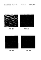
- FIG. 5a is a photomicrograph of an ion-implanted surface of a GaAs semiconductor which was uncovered during the annealing process.
- FIG. 5b is a photomicrograph of the ion-implanted surface of a GaAs semiconductor which was annealed according to the present invention.
- FIG. 6a is a photomicrograph of an ion-implanted surface of an InP semiconductor which was uncovered during annealing.
- FIG. 6b is a photomicrograph of an ion-implanted surface of an InP semiconductor which was annealed according to the present invention.
- the process described herein relates to the annealing of N or P-type GaAs or InP semiconductor materials (wafers) which have already had one of their plane surfaces polished and implanted with ions by any one of the well-known methods in the art.
- semiconductor wafer 10 is sandwiched between somewhat larger top and bottom covering pieces which are identified generally by numerals 12 and 14, respectively.
- One type of semiconductor 10 may be chromium (Cr) doped GaAs material with one of its planar surfaces or faces polished and implanted with beryllium (Be + ) ions.
- Another type of semiconductor 10 may be iron (Fe) doped InP material with one of its planar surfaces implanted with silicon (Si + ) or selenium ions (Se + ).
- the semiconductor is positioned between the covering pieces as shown in FIG. 1, preferable with its ion-implanted surface facing the bottom covering piece 14.
- Top covering piece 12 which may be identical to the bottom covering piece, serves only as a nonreactive mass to help maintain the semiconductor 10 in face-to-face contact with the surface of bottom covering piece 14.
- FIG. 2 An alternate arrangement is shown in FIG. 2 where the semiconductor 10 is positioned with its ion-implanted surface facing down on bottom covering piece 14, without the benefit of a top covering piece.
- the surface areas of the covering pieces, and particularly the covering piece facing the ion-implanted surface, are somewhat greater than the surface area of semiconductor wafer or chip 10.
- the covering pieces may each be formed of a semiconductor material (not shown) identical to that of the wafer or chip being annealed.
- each covering piece may be made in another form for serving their purpose in the annealing process.
- each covering piece includes a backing or substrate 18 covered by a deposit or overlay 20.
- the substrate may be a material identical to the semiconductor material (GaAs or InP) to be annealed with its surface polished to a smoothness substantially matching that on the semiconductor surface and have a thin coating of silicon nitride (Si 3 N 4 ) applied thereon.
- Si 3 N 4 silicon nitride
- the top piece serving as a mass, need only be formed of a material nonreactive with Si 3 N 4 , GaAs or InP. But, for convenience both covering pieces are preferable identical.
- substrate 18 may be formed of silicon (Si) and overlaid with a dielectric material such as silicon nitride (Si 3 N 4 ), quartz (SiO 2 ), or aluminum nitride (AIN). It is essential that all these materials be nonreactive with GaAs or InP at the elevated annealing temperatures.
- a dielectric material such as silicon nitride (Si 3 N 4 ), quartz (SiO 2 ), or aluminum nitride (AIN). It is essential that all these materials be nonreactive with GaAs or InP at the elevated annealing temperatures.
- semiconductor wafer 10 lies centrally disposed on covering piece 14 with its ion-implanted surface facing downward.
- the semiconductors own weight is sufficient to maintain it in position and in face-to-face contact with the covering piece during the annealing process.
- the apparatus and steps involved in the present annealing process for ion-implanted semiconductor wafers 10 as arranged in FIGS. 1 and 2 will now be described.
- the semiconductor which has been ion-implanted across its entire surface together with its covering piece or pieces, is placed in a small quartz bottle 22 shown in FIG. 3.
- the bottle is then loaded into the cold part 24 of annealing tube 26 and remains open during a purging period.
- Forming gas (15% H 2 and 85% N 2 ) provides the ambient environment.
- the bottle is pushed into the hot section 28 of furnace 30 and tightly closed.
- the semiconductor wafers are annealed at elevated temperatures, depending on whether GaAs or InP material, for around 10-20 minutes.
- annealing bottle 22 is pulled back to the cold section 24 where it remains closed until it has reached room temperature.
- the gas inside the bottle is then changed to N 2 and the annealed wafer or chip is removed from the bottle.
- the semiconductor material is ion-implanted across its entire surface. It is desirable that this surface, when annealed, exhibit a surface free of pock marks left by evaporation. Therefore, the covering pieces preferable have a larger area then the semiconductors wafer or chip so that they extend beyond the peripheral edges thereof to assure proper annealing across its entire surface.
- the annealing temperature and time is dependent upon ion concentration. Generally, GaAs semiconductor wafers are annealed at around 800° to 1000° for 15 to 20 minutes and InP semiconductor wafers are annealed at around 700° to 800° C. for 10 to 20 minutes.
- FIGS. 5a and 5b are photomicrograph providing a basis for making a comparsion of the morphology of two identical Cr + -doped, Be + -implanted GaAs substrates which were heated together at 800° C. for 25 minutes.
- FIG. 6a and 6b A comparision of the morphology of two identical ion-implanted substrates of InP may be made from FIG. 6a and 6b. These samples were implanted with 2.16 ⁇ 10 12 /cm 2 , 100 KeV and 6.45 ⁇ 10 12 /cm 2 , 240 KeV 29Si ions. The dual implantation was performed in order to achieve a uniform silicon donor concentration of 1.8 ⁇ 10 17 /cm 3 level over 4000 A thickness. The wafers were annealed at 760° C. for 15 minutes. The sample shown in the FIG. 6a photomicrograph (6000X) was annealed unprotected and exposed directly to the ambient. The sample shown in the FIG. 6b photomicrograph (6000X) was covered in face-to-face contact with Si 3 N 4 covered InP. There is no resolvable morphogical feature.
Abstract
A method of annealing both N and P-type ion-implanted GaAs and InP semiconductors by using a close-contact capping technique. A flat polished ion-implanted surface on a gallium arsenide (GaAs) or indium phosphide (InP) semiconductor is placed in face-to-face contact with a non-reactive flat surface such as Si3 N4, SiO2, AlN, or identical semiconductor material, and annealed at selected elevated temperatures and time dependent upon ion concentration. The annealed semiconductor material, usually in the form of a wafer, is allowed to cool to room temperature for further processing.
Description
There is considerable interest in ion-implantation doping of GaAs and InP, especially for microwave uses. Ion-Implantation is considered to be an alternative to diffusion for the creation of a heavily doped thin region beneath the surface of the seimconductor material. Heat treating GaAs or InP is necessary after most ion-implantations for two purposes: (1) to increase the electrical activity of the implanted ions; and (2) to remove the lattice damage caused in the material by the ions during their implantation.
It has been learned that ion-implanted semiconductors during annealing undergo incongruent evaporation at temperatures lower than their annealing temperatures. Therefore, it is now standard practice to encapsulate the semiconductors with suitable dielectric layers during annealing, or to anneal the semiconductors in a carefully controlled environment to prevent evaporation from their surfaces. In all cases, the goal has been to develop an annealing process which preserves the chemical and electrical properties of the implanted material during high temperature annealing, while providing high mobility and activation of the implanted semiconductor material.
Prior methods of annealing smooth surfaces of ion-implanted GaAs or InP have often involved a step of depositing a dielectric encapsulating film of thermal matching characteristics on the implanted surface, and removing it after annealing.
The process disclosed herein relates to annealing ion-implanted GaAs and InP semiconductor wafers. The flat ion-implanted surface on the semiconductor is covered by another flat surface (nonreactive) in close contact therewith during the annealing process. The covering material may be identical semiconductor material provided with a surface of the same general smoothness to allow for the necessary close physical contact. In the alternative, the covering may be the same material, polished to the same smoothness as the unannealed semiconductor, covered with a thin coat of dielectric material such as Si3 N4, SiO2 or AlN, which actually contacts the ion-implanted surface.
It is therefore an object of this invention to provide a method of annealing ion-implanted semiconductor wafers.
It is another object of this invention to provide a method of annealing ion-implanted semiconductor wafers wherein the unannealed surface is overlaid by a like material to prevent evaporation during the annealing steps.
It is still another object of this invention to provide a method of annealing ion-implanted semiconductor wafers wherein the unannealed surface is overlaid by a like material which is covered by another dielectric material to prevent evaporation during the annealing steps.
Other objects of the invention will become apparent after consideration of the specification and claims in conjunction with the drawings.
FIG. 1 is a perspective view of an ion-implanted semiconductor material wafer or slice sandwiched between two covering pieces.
FIG. 2 is a perspective view of an ion-implanted semiconductor material (wafer or slice) positioned atop a covering piece.
FIG. 3 illustrates a quartz bottle which is used for holding the semiconductor material and covering piece or pieces during annealing.
FIG. 4 illustrates annealing equipment including purging apparatus and a furnace.
FIG. 5a is a photomicrograph of an ion-implanted surface of a GaAs semiconductor which was uncovered during the annealing process.
FIG. 5b is a photomicrograph of the ion-implanted surface of a GaAs semiconductor which was annealed according to the present invention.
FIG. 6a is a photomicrograph of an ion-implanted surface of an InP semiconductor which was uncovered during annealing.
FIG. 6b is a photomicrograph of an ion-implanted surface of an InP semiconductor which was annealed according to the present invention.
The process described herein relates to the annealing of N or P-type GaAs or InP semiconductor materials (wafers) which have already had one of their plane surfaces polished and implanted with ions by any one of the well-known methods in the art.
As shown in FIG. 1, semiconductor wafer 10 is sandwiched between somewhat larger top and bottom covering pieces which are identified generally by numerals 12 and 14, respectively. One type of semiconductor 10 may be chromium (Cr) doped GaAs material with one of its planar surfaces or faces polished and implanted with beryllium (Be+) ions. Another type of semiconductor 10 may be iron (Fe) doped InP material with one of its planar surfaces implanted with silicon (Si+) or selenium ions (Se+). The semiconductor is positioned between the covering pieces as shown in FIG. 1, preferable with its ion-implanted surface facing the bottom covering piece 14. Top covering piece 12, which may be identical to the bottom covering piece, serves only as a nonreactive mass to help maintain the semiconductor 10 in face-to-face contact with the surface of bottom covering piece 14.
An alternate arrangement is shown in FIG. 2 where the semiconductor 10 is positioned with its ion-implanted surface facing down on bottom covering piece 14, without the benefit of a top covering piece. The surface areas of the covering pieces, and particularly the covering piece facing the ion-implanted surface, are somewhat greater than the surface area of semiconductor wafer or chip 10. When the wafer or chip is centrally positioned on or between the covering, as shown in FIGS. 1 and 2, there is defined an overhanging or shelf-like peripheral surface 16 at hereabout. The covering pieces may each be formed of a semiconductor material (not shown) identical to that of the wafer or chip being annealed.
The covering pieces may be made in another form for serving their purpose in the annealing process. As shown in FIGS. 1 and 2, each covering piece includes a backing or substrate 18 covered by a deposit or overlay 20. The substrate may be a material identical to the semiconductor material (GaAs or InP) to be annealed with its surface polished to a smoothness substantially matching that on the semiconductor surface and have a thin coating of silicon nitride (Si3 N4) applied thereon. Obviously only one covering piece (bottom) need be so formed because the other covering piece (top) is not in contact with the ion-implanted surface. The top piece, serving as a mass, need only be formed of a material nonreactive with Si3 N4, GaAs or InP. But, for convenience both covering pieces are preferable identical.
Several alternative arrangements are possible, all within the scope of this invention. For example, substrate 18 may be formed of silicon (Si) and overlaid with a dielectric material such as silicon nitride (Si3 N4), quartz (SiO2), or aluminum nitride (AIN). It is essential that all these materials be nonreactive with GaAs or InP at the elevated annealing temperatures.
As shown in FIG. 2 semiconductor wafer 10 lies centrally disposed on covering piece 14 with its ion-implanted surface facing downward. The semiconductors own weight is sufficient to maintain it in position and in face-to-face contact with the covering piece during the annealing process.
The apparatus and steps involved in the present annealing process for ion-implanted semiconductor wafers 10 as arranged in FIGS. 1 and 2 will now be described. The semiconductor, which has been ion-implanted across its entire surface together with its covering piece or pieces, is placed in a small quartz bottle 22 shown in FIG. 3. The bottle is then loaded into the cold part 24 of annealing tube 26 and remains open during a purging period. Forming gas (15% H2 and 85% N2) provides the ambient environment. After several minutes of purging the bottle is pushed into the hot section 28 of furnace 30 and tightly closed. The semiconductor wafers are annealed at elevated temperatures, depending on whether GaAs or InP material, for around 10-20 minutes. After annealing bottle 22 is pulled back to the cold section 24 where it remains closed until it has reached room temperature. The gas inside the bottle is then changed to N2 and the annealed wafer or chip is removed from the bottle. The semiconductor material is ion-implanted across its entire surface. It is desirable that this surface, when annealed, exhibit a surface free of pock marks left by evaporation. Therefore, the covering pieces preferable have a larger area then the semiconductors wafer or chip so that they extend beyond the peripheral edges thereof to assure proper annealing across its entire surface.
The annealing temperature and time is dependent upon ion concentration. Generally, GaAs semiconductor wafers are annealed at around 800° to 1000° for 15 to 20 minutes and InP semiconductor wafers are annealed at around 700° to 800° C. for 10 to 20 minutes.
Semiconductor wafers used in tests were all (100) orientated substrates of GaAs or InP. For electrical measurements, either chromium doped GaAs or iron doped InP semi-insulation substrates were used. The wafers were Be+ ion-implanted for P-type dopant and Si+ or Se+ ion-implanted for N-type dopant. The substrates were at room temperature during the ion-implantation. FIGS. 5a and 5b are photomicrograph providing a basis for making a comparsion of the morphology of two identical Cr+ -doped, Be+ -implanted GaAs substrates which were heated together at 800° C. for 25 minutes. Each surface had been previously etched and polished and was implanted with 5.58×10¹⁵ /cm2 150-KeV Be+ ions. The surface shown in the photomicrograph (6000X) of FIG. 5a was left uncovered and exposed to the ambient during the annealing process. It is obvious from an examination that its surface had undergone severe evaporation which left the previously polished surface highly pocked. The photomicrograph in FIG. 5b shows the companion substrate at 6000X as having no discernible morphological features.
A comparision of the morphology of two identical ion-implanted substrates of InP may be made from FIG. 6a and 6b. These samples were implanted with 2.16×10¹² /cm2, 100 KeV and 6.45×10¹² /cm2, 240 KeV 29Si ions. The dual implantation was performed in order to achieve a uniform silicon donor concentration of 1.8×10¹⁷ /cm3 level over 4000 A thickness. The wafers were annealed at 760° C. for 15 minutes. The sample shown in the FIG. 6a photomicrograph (6000X) was annealed unprotected and exposed directly to the ambient. The sample shown in the FIG. 6b photomicrograph (6000X) was covered in face-to-face contact with Si3 N4 covered InP. There is no resolvable morphogical feature.
The process described therein is effective for the electrical activation of ion-implanted GaAs and InP. The results indicate (FIGS. 5b and 6b) that there is very little evaporation from the surfaces of the samples when they are annealed according to the method of the invention disclosed and claimed herein.
The invention is directed to alternate embodiments for annealing two different ion-implanted semiconductor materials and has been described herein in considerable detail. It will be understood that variations and modifications can be made to the method without departing from the spirit and scope of the invention, which is limited only by the scope of the claims annexed hereto.
Claims (8)
1. A process of annealing ion-implanted semiconductor material comprising the steps of:
selecting an unannealed semiconductor material having an ion-implanted polished surface;
selecting a like semiconductor material having a polished surface larger than that of the first-mentioned surface;
positioning the unannealed semiconductor material in surface-to-surface contact with the larger surface which extends beyond the periphery of the smaller surface;
maintaining the surfaces in contact; and
annealing the ion-implanted semiconductor material substantially in the absence of oxygen whereby evaporation of material from the implanted surface is minimized.
2. A process of annealing an ion-implanted semiconductor material comprising:
selecting an unannealed semiconductor material from the group consisting of GaAs and InP having a polished surface implanted with ions selected from the group consisting of Be+, 29Si+ and Se+ ;
selecting a like semiconductor material having a surface area greater than the area of the ion-implanted surface and provided with a coating of dielectric material on the surface selected from the group consisting of Si3 N4, SiO2 and AlN polished to a smoothness substantially matching that of the first mentioned surface;
positioning the surfaces in face-to-face contact with peripherial portions of the larger surface surrounding the, smaller surface;
maintaining the surfaces in contact; and
annealing the ion-implanted semiconductor material in an atmosphere of nitrogen and hydrogen whereby evaporation of material from the implanted surface is minimized.
3. The process according to claim 2 comprising a further step of selecting an annealing atmosphere of approximately 15% H2 and 85% N2.
4. The process according to claim 2 or 3 comprising annealing the ion-implanted semiconductor material at a temperature of about 800°-1000° C. for about 15-20 minutes when the material is GaAs.
5. The process according to claim 2 or 3 comprising annealing the ion-implanted semiconductor material to a temperature of about 700°-800° C. for about 15-20 minutes when the material is InP.
6. A process of annealing a wafer of ion-implanted semiconductor material comprising the steps of:
selecting an unannealed semiconductor wafer selected from the group consisting of GaAs and InP having a polished planar surface implanted with ions selected from the group consisting of Be+, 29Si+ and Se+ ;
coating a Si matrix with a layer of dielectric material selected from the group consisting of Si3 N4, SiO2 and AlN;
providing a polished planar surface on the dielectric material having an area larger than the area of the planar surface on the semiconductor wafer;
positioning the polished surfaces together in face-to-face contact with excess area of the larger planar surface extending beyond the outer periphery of the smaller planar surface;
maintaining the surfaces in face-to-face contact;
planning the positioned materials into a container;
purging the container to have an embient environment gas of approximately 15% H2 and 85% N2 ;
placing the container in a furnace at an elevated temperature for a predetermined time;
removing the container from the furnace and allowing the materials to cool to substantially room temperature;
changing the ambient gas to N2 ; and
removing the annealed semiconductor.
7. The process according to claim 6 comprising the step of maintaining a GaAs ion-implanted semiconductor wafer at a temperature of 800°-1000° C. for about 15-20 minutes.
8. The process according to claim 6 comprising the step of maintaining an InP ion-implanted semiconductor wafer at a temperature of 700°-800° C. for about 15-20 minutes.
Priority Applications (1)
| Application Number | Priority Date | Filing Date | Title |
|---|---|---|---|
| US06/228,425 US4357180A (en) | 1981-01-26 | 1981-01-26 | Annealing of ion-implanted GaAs and InP semiconductors |
Applications Claiming Priority (1)
| Application Number | Priority Date | Filing Date | Title |
|---|---|---|---|
| US06/228,425 US4357180A (en) | 1981-01-26 | 1981-01-26 | Annealing of ion-implanted GaAs and InP semiconductors |
Publications (1)
| Publication Number | Publication Date |
|---|---|
| US4357180A true US4357180A (en) | 1982-11-02 |
Family
ID=22857118
Family Applications (1)
| Application Number | Title | Priority Date | Filing Date |
|---|---|---|---|
| US06/228,425 Expired - Fee Related US4357180A (en) | 1981-01-26 | 1981-01-26 | Annealing of ion-implanted GaAs and InP semiconductors |
Country Status (1)
| Country | Link |
|---|---|
| US (1) | US4357180A (en) |
Cited By (23)
| Publication number | Priority date | Publication date | Assignee | Title |
|---|---|---|---|---|
| US4396437A (en) * | 1981-05-04 | 1983-08-02 | Hughes Aircraft Company | Selective encapsulation, controlled atmosphere annealing for III-V semiconductor device fabrication |
| US4473939A (en) * | 1982-12-27 | 1984-10-02 | Hughes Aircraft Company | Process for fabricating GaAs FET with ion implanted channel layer |
| US4489480A (en) * | 1982-04-09 | 1984-12-25 | U.S. Philips Corporation | Method of manufacturing field effect transistors of GaAs by ion implantation |
| US4555273A (en) * | 1984-02-27 | 1985-11-26 | The United States Of America As Represented By The Secretary Of The Navy | Furnace transient anneal process |
| US4595423A (en) * | 1983-09-09 | 1986-06-17 | Nippon Telegraph & Telephone Public Corporation | Method of homogenizing a compound semiconductor crystal prior to implantation |
| US4636280A (en) * | 1983-08-23 | 1987-01-13 | Sumitomo Electric Ind., Ltd. | Method for the pretreatment of a substrate for ion implantation |
| US4676840A (en) * | 1984-09-06 | 1987-06-30 | Nec Corporation | Method of capless annealing for group III-V compound semiconductor substrate |
| US4713354A (en) * | 1985-02-28 | 1987-12-15 | Oki Electric Industry Co., Ltd. | Method of heat treatment for reduction of dislocation density near III-V substrate surface |
| US4772489A (en) * | 1985-09-20 | 1988-09-20 | Sumitomo Electric Industries, Ltd. | Method of annealing a compound semiconductor substrate |
| US4830987A (en) * | 1987-11-19 | 1989-05-16 | Texas Instruments Incorporated | Contactless annealing process using cover slices |
| US4929564A (en) * | 1988-10-21 | 1990-05-29 | Nippon Mining Co., Ltd. | Method for producing compound semiconductor single crystals and method for producing compound semiconductor devices |
| US5017508A (en) * | 1989-06-29 | 1991-05-21 | Ixys Corporation | Method of annealing fully-fabricated, radiation damaged semiconductor devices |
| US5034343A (en) * | 1990-03-08 | 1991-07-23 | Harris Corporation | Manufacturing ultra-thin wafer using a handle wafer |
| US5047370A (en) * | 1988-10-31 | 1991-09-10 | Nippon Mining Co., Ltd. | Method for producing compound semiconductor single crystal substrates |
| US5093284A (en) * | 1988-05-27 | 1992-03-03 | Hitachi Chemical Company, Ltd. | Process for homogenizing compound semiconductor single crystal in properties |
| US5115294A (en) * | 1989-06-29 | 1992-05-19 | At&T Bell Laboratories | Optoelectronic integrated circuit |
| US5162242A (en) * | 1989-03-27 | 1992-11-10 | Matsushita Electric Industrial Co., Ltd. | Method for annealing compound semiconductor devices |
| WO1995026042A1 (en) * | 1994-03-24 | 1995-09-28 | Starfire Electronic Development & Marketing, Ltd. | Thin film electronic devices and manufacturing method |
| US5520785A (en) * | 1994-01-04 | 1996-05-28 | Motorola, Inc. | Method for enhancing aluminum nitride |
| US5614447A (en) * | 1994-11-30 | 1997-03-25 | New Japan Radio Co., Ltd. | Method for heat-treating a semiconductor body |
| US5650353A (en) * | 1992-09-29 | 1997-07-22 | Shin-Etsu Handotai Co., Ltd. | Method for production of SOI substrate |
| US20070190757A1 (en) * | 2004-02-17 | 2007-08-16 | Nippon Mining & Metals Co., Ltd. | Vapor phase growth method |
| CN112899790A (en) * | 2021-01-15 | 2021-06-04 | 中国科学院半导体研究所 | Annealing method for removing residual stress of gallium antimonide single crystal wafer |
Citations (10)
| Publication number | Priority date | Publication date | Assignee | Title |
|---|---|---|---|---|
| US3547635A (en) * | 1967-05-04 | 1970-12-15 | Eastman Kodak Co | Vacuum deposited light-sensitive titanium dioxide |
| US3644154A (en) * | 1969-06-09 | 1972-02-22 | Ibm | Method of fabricating semiconductor structures with reduced crystallographic defects |
| US3720515A (en) * | 1971-10-20 | 1973-03-13 | Trw Inc | Microelectronic circuit production |
| US3737282A (en) * | 1971-10-01 | 1973-06-05 | Ibm | Method for reducing crystallographic defects in semiconductor structures |
| US3762945A (en) * | 1972-05-01 | 1973-10-02 | Bell Telephone Labor Inc | Technique for the fabrication of a millimeter wave beam lead schottkybarrier device |
| US3984263A (en) * | 1973-10-19 | 1976-10-05 | Matsushita Electric Industrial Co., Ltd. | Method of producing defectless epitaxial layer of gallium |
| US4016006A (en) * | 1974-10-30 | 1977-04-05 | Hitachi, Ltd. | Method of heat treatment of wafers |
| US4155784A (en) * | 1977-04-08 | 1979-05-22 | Trw Inc. | Process for epitaxially growing a gallium arsenide layer having reduced silicon contaminants on a gallium arsenide substrate |
| US4173063A (en) * | 1976-07-15 | 1979-11-06 | Siemens Aktiengesellschaft | Fabrication of a semiconductor component element having a Schottky contact and little series resistance utilizing special masking in combination with ion implantation |
| US4179533A (en) * | 1978-04-25 | 1979-12-18 | The United States Of America As Represented By The Secretary Of The Navy | Multi-refractory films for gallium arsenide devices |
-
1981
- 1981-01-26 US US06/228,425 patent/US4357180A/en not_active Expired - Fee Related
Patent Citations (10)
| Publication number | Priority date | Publication date | Assignee | Title |
|---|---|---|---|---|
| US3547635A (en) * | 1967-05-04 | 1970-12-15 | Eastman Kodak Co | Vacuum deposited light-sensitive titanium dioxide |
| US3644154A (en) * | 1969-06-09 | 1972-02-22 | Ibm | Method of fabricating semiconductor structures with reduced crystallographic defects |
| US3737282A (en) * | 1971-10-01 | 1973-06-05 | Ibm | Method for reducing crystallographic defects in semiconductor structures |
| US3720515A (en) * | 1971-10-20 | 1973-03-13 | Trw Inc | Microelectronic circuit production |
| US3762945A (en) * | 1972-05-01 | 1973-10-02 | Bell Telephone Labor Inc | Technique for the fabrication of a millimeter wave beam lead schottkybarrier device |
| US3984263A (en) * | 1973-10-19 | 1976-10-05 | Matsushita Electric Industrial Co., Ltd. | Method of producing defectless epitaxial layer of gallium |
| US4016006A (en) * | 1974-10-30 | 1977-04-05 | Hitachi, Ltd. | Method of heat treatment of wafers |
| US4173063A (en) * | 1976-07-15 | 1979-11-06 | Siemens Aktiengesellschaft | Fabrication of a semiconductor component element having a Schottky contact and little series resistance utilizing special masking in combination with ion implantation |
| US4155784A (en) * | 1977-04-08 | 1979-05-22 | Trw Inc. | Process for epitaxially growing a gallium arsenide layer having reduced silicon contaminants on a gallium arsenide substrate |
| US4179533A (en) * | 1978-04-25 | 1979-12-18 | The United States Of America As Represented By The Secretary Of The Navy | Multi-refractory films for gallium arsenide devices |
Non-Patent Citations (6)
| Title |
|---|
| Immorlica et al., Appl. Phys. Letts. 29, (1976), 94. * |
| Kasahaka, Arai, Wattanabe; "Capless Anneal of Ion-Implanted GaAs in Controlled Arsenic Vapor"; J. Appl. Physc. 50 (1); Jan. 1979; pp. 541-543. * |
| Malbon, Lee, Whelan; "Annealing of Ion-Implanted GaAs in a Controlled Atmhere"; J. Electrochem. Soc.: Solid-State Science and Tech.; vol. 123, No. 9; Sep. 1976; pp. 1413-1415. |
| Malbon, Lee, Whelan; "Annealing of Ion-Implanted GaAs in a Controlled Atmhere"; J. Electrochem. Soc.: Solid-State Science and Tech.; vol. 123, No. 9; Sep. 1976; pp. 1413-1415. * |
| Sealy, Surridge; "A New Thin Film Encapsulant for Ion-Implanted GaAs", Thin Solid Films, 26, (1975), L19-L-22; Switzerland. * |
| Woodall et al., IBM-TDB, 10 (1968), 1476. * |
Cited By (24)
| Publication number | Priority date | Publication date | Assignee | Title |
|---|---|---|---|---|
| US4396437A (en) * | 1981-05-04 | 1983-08-02 | Hughes Aircraft Company | Selective encapsulation, controlled atmosphere annealing for III-V semiconductor device fabrication |
| US4489480A (en) * | 1982-04-09 | 1984-12-25 | U.S. Philips Corporation | Method of manufacturing field effect transistors of GaAs by ion implantation |
| US4473939A (en) * | 1982-12-27 | 1984-10-02 | Hughes Aircraft Company | Process for fabricating GaAs FET with ion implanted channel layer |
| US4636280A (en) * | 1983-08-23 | 1987-01-13 | Sumitomo Electric Ind., Ltd. | Method for the pretreatment of a substrate for ion implantation |
| US4595423A (en) * | 1983-09-09 | 1986-06-17 | Nippon Telegraph & Telephone Public Corporation | Method of homogenizing a compound semiconductor crystal prior to implantation |
| US4555273A (en) * | 1984-02-27 | 1985-11-26 | The United States Of America As Represented By The Secretary Of The Navy | Furnace transient anneal process |
| US4676840A (en) * | 1984-09-06 | 1987-06-30 | Nec Corporation | Method of capless annealing for group III-V compound semiconductor substrate |
| US4713354A (en) * | 1985-02-28 | 1987-12-15 | Oki Electric Industry Co., Ltd. | Method of heat treatment for reduction of dislocation density near III-V substrate surface |
| US4772489A (en) * | 1985-09-20 | 1988-09-20 | Sumitomo Electric Industries, Ltd. | Method of annealing a compound semiconductor substrate |
| US4830987A (en) * | 1987-11-19 | 1989-05-16 | Texas Instruments Incorporated | Contactless annealing process using cover slices |
| US5093284A (en) * | 1988-05-27 | 1992-03-03 | Hitachi Chemical Company, Ltd. | Process for homogenizing compound semiconductor single crystal in properties |
| US4929564A (en) * | 1988-10-21 | 1990-05-29 | Nippon Mining Co., Ltd. | Method for producing compound semiconductor single crystals and method for producing compound semiconductor devices |
| US5047370A (en) * | 1988-10-31 | 1991-09-10 | Nippon Mining Co., Ltd. | Method for producing compound semiconductor single crystal substrates |
| US5162242A (en) * | 1989-03-27 | 1992-11-10 | Matsushita Electric Industrial Co., Ltd. | Method for annealing compound semiconductor devices |
| US5017508A (en) * | 1989-06-29 | 1991-05-21 | Ixys Corporation | Method of annealing fully-fabricated, radiation damaged semiconductor devices |
| US5115294A (en) * | 1989-06-29 | 1992-05-19 | At&T Bell Laboratories | Optoelectronic integrated circuit |
| US5034343A (en) * | 1990-03-08 | 1991-07-23 | Harris Corporation | Manufacturing ultra-thin wafer using a handle wafer |
| US5650353A (en) * | 1992-09-29 | 1997-07-22 | Shin-Etsu Handotai Co., Ltd. | Method for production of SOI substrate |
| US5520785A (en) * | 1994-01-04 | 1996-05-28 | Motorola, Inc. | Method for enhancing aluminum nitride |
| WO1995026042A1 (en) * | 1994-03-24 | 1995-09-28 | Starfire Electronic Development & Marketing, Ltd. | Thin film electronic devices and manufacturing method |
| US5614447A (en) * | 1994-11-30 | 1997-03-25 | New Japan Radio Co., Ltd. | Method for heat-treating a semiconductor body |
| US20070190757A1 (en) * | 2004-02-17 | 2007-08-16 | Nippon Mining & Metals Co., Ltd. | Vapor phase growth method |
| US7883998B2 (en) * | 2004-02-17 | 2011-02-08 | Nippon Mining & Metals Co., Ltd. | Vapor phase growth method |
| CN112899790A (en) * | 2021-01-15 | 2021-06-04 | 中国科学院半导体研究所 | Annealing method for removing residual stress of gallium antimonide single crystal wafer |
Similar Documents
| Publication | Publication Date | Title |
|---|---|---|
| US4357180A (en) | Annealing of ion-implanted GaAs and InP semiconductors | |
| CA1180256A (en) | Annealing of ion implanted iii-v compounds | |
| EP0558554B1 (en) | Silicon-on-porous-silicon; method of production and material | |
| Molnar | Close‐contact annealing of ion‐implanted GaAs and InP | |
| Evans Jr et al. | Redistribution of Cr during annealing of 80Se‐implanted GaAs | |
| US4469528A (en) | Method of manufacturing a semiconductor device of GaAs by two species ion implantation | |
| JPH0587036B2 (en) | ||
| Cummings et al. | Rapid annealing of GaAs: Uniformity and temperature dependence of activation | |
| de Souza et al. | Ion implantation in gallium arsenide MESFET technology | |
| Schwarz et al. | Annealing behavior of ion‐implanted Fe in InP | |
| US4820651A (en) | Method of treating bodies of III-V compound semiconductor material | |
| Feng et al. | Study of electrical and chemical profiles of Si implanted in semi‐insulating GaAs substrate annealed under SiO2 and capless | |
| Liu et al. | Rapid capless annealing of 28 Si, 64 Zn, and 9 Be implants in GaAs | |
| Kato | The Annealing Time and Temperature Dependence of Electrical Dopant Activation in High‐Dose BF 2 Ion Implanted Silicon | |
| Ottaviani et al. | Some aspects of Ge epitaxial growth by solid solution | |
| Thompson et al. | MeV S implantation into GaAs | |
| Pearton et al. | Transient thermal processing of GaAs | |
| Sharma | Ion implantation into GaAs | |
| Masum Choudhury et al. | Formation of p‐type GaAs layers using Mg+ implantation and capless rapid thermal annealing | |
| Kamins et al. | Effect of Hydrogen on p‐Type Epitaxial Silicon Sheet‐Resistance Measurements | |
| Miyake et al. | Defects induced by deep preamorphization and their effects on metal oxide semiconductor device characteristics | |
| US4302278A (en) | GaAs Crystal surface passivation method | |
| JPH03110833A (en) | Heat treatment of compound semiconductor | |
| Yagita et al. | Cr gettering by Ne ion implantation and the correlation with the electrical activation of implanted Si in semi‐insulating GaAs | |
| Birey et al. | Photoluminescence of gallium arsenide encapsulated with aluminum nitride and silicon nitride |
Legal Events
| Date | Code | Title | Description |
|---|---|---|---|
| AS | Assignment |
Owner name: UNITED STATES OF AMERICA, AS REPRESENTED BY THE SE Free format text: ASSIGNMENT OF ASSIGNORS INTEREST;ASSIGNOR:MOLNAR BELA;REEL/FRAME:003858/0816 Effective date: 19810123 |
|
| FEPP | Fee payment procedure |
Free format text: MAINTENANCE FEE REMINDER MAILED (ORIGINAL EVENT CODE: REM.); ENTITY STATUS OF PATENT OWNER: LARGE ENTITY |
|
| LAPS | Lapse for failure to pay maintenance fees | ||
| STCH | Information on status: patent discontinuation |
Free format text: PATENT EXPIRED DUE TO NONPAYMENT OF MAINTENANCE FEES UNDER 37 CFR 1.362 |
|
| FP | Lapsed due to failure to pay maintenance fee |
Effective date: 19861102 |