US4513219A - Vibration wave motor - Google Patents
Vibration wave motor Download PDFInfo
- Publication number
- US4513219A US4513219A US06/552,373 US55237383A US4513219A US 4513219 A US4513219 A US 4513219A US 55237383 A US55237383 A US 55237383A US 4513219 A US4513219 A US 4513219A
- Authority
- US
- United States
- Prior art keywords
- electro
- strain element
- pair
- element groups
- vibration wave
- Prior art date
- Legal status (The legal status is an assumption and is not a legal conclusion. Google has not performed a legal analysis and makes no representation as to the accuracy of the status listed.)
- Expired - Lifetime
Links
- 239000006096 absorbing agent Substances 0.000 claims description 20
- 239000012212 insulator Substances 0.000 claims description 6
- 230000004044 response Effects 0.000 claims description 5
- 230000033001 locomotion Effects 0.000 description 11
- 229910052751 metal Inorganic materials 0.000 description 6
- 239000002184 metal Substances 0.000 description 6
- 244000145845 chattering Species 0.000 description 4
- 239000011295 pitch Substances 0.000 description 4
- 230000001960 triggered effect Effects 0.000 description 4
- 102100029469 WD repeat and HMG-box DNA-binding protein 1 Human genes 0.000 description 3
- 101710097421 WD repeat and HMG-box DNA-binding protein 1 Proteins 0.000 description 3
- 238000010521 absorption reaction Methods 0.000 description 3
- 230000002441 reversible effect Effects 0.000 description 3
- 238000005299 abrasion Methods 0.000 description 2
- 230000008859 change Effects 0.000 description 2
- 238000004519 manufacturing process Methods 0.000 description 2
- 238000005259 measurement Methods 0.000 description 2
- 230000004048 modification Effects 0.000 description 2
- 238000012986 modification Methods 0.000 description 2
- 230000010363 phase shift Effects 0.000 description 2
- 230000010287 polarization Effects 0.000 description 2
- 230000035945 sensitivity Effects 0.000 description 2
- 229910000679 solder Inorganic materials 0.000 description 2
- 230000001360 synchronised effect Effects 0.000 description 2
- 229910018404 Al2 O3 Inorganic materials 0.000 description 1
- PNEYBMLMFCGWSK-UHFFFAOYSA-N Alumina Chemical compound [O-2].[O-2].[O-2].[Al+3].[Al+3] PNEYBMLMFCGWSK-UHFFFAOYSA-N 0.000 description 1
- 229920001875 Ebonite Polymers 0.000 description 1
- 230000004913 activation Effects 0.000 description 1
- 229910052782 aluminium Inorganic materials 0.000 description 1
- XAGFODPZIPBFFR-UHFFFAOYSA-N aluminium Chemical compound [Al] XAGFODPZIPBFFR-UHFFFAOYSA-N 0.000 description 1
- 239000000919 ceramic Substances 0.000 description 1
- 230000005484 gravity Effects 0.000 description 1
- 238000009413 insulation Methods 0.000 description 1
- WABPQHHGFIMREM-UHFFFAOYSA-N lead(0) Chemical compound [Pb] WABPQHHGFIMREM-UHFFFAOYSA-N 0.000 description 1
- 230000007246 mechanism Effects 0.000 description 1
- 239000012811 non-conductive material Substances 0.000 description 1
- 230000000737 periodic effect Effects 0.000 description 1
- 238000005476 soldering Methods 0.000 description 1
- 125000006850 spacer group Chemical group 0.000 description 1
- 230000003746 surface roughness Effects 0.000 description 1
- 238000004804 winding Methods 0.000 description 1
Images


Classifications
-
- H—ELECTRICITY
- H02—GENERATION; CONVERSION OR DISTRIBUTION OF ELECTRIC POWER
- H02N—ELECTRIC MACHINES NOT OTHERWISE PROVIDED FOR
- H02N2/00—Electric machines in general using piezoelectric effect, electrostriction or magnetostriction
- H02N2/10—Electric machines in general using piezoelectric effect, electrostriction or magnetostriction producing rotary motion, e.g. rotary motors
- H02N2/14—Drive circuits; Control arrangements or methods
- H02N2/145—Large signal circuits, e.g. final stages
- H02N2/147—Multi-phase circuits
-
- H—ELECTRICITY
- H02—GENERATION; CONVERSION OR DISTRIBUTION OF ELECTRIC POWER
- H02N—ELECTRIC MACHINES NOT OTHERWISE PROVIDED FOR
- H02N2/00—Electric machines in general using piezoelectric effect, electrostriction or magnetostriction
- H02N2/10—Electric machines in general using piezoelectric effect, electrostriction or magnetostriction producing rotary motion, e.g. rotary motors
- H02N2/16—Electric machines in general using piezoelectric effect, electrostriction or magnetostriction producing rotary motion, e.g. rotary motors using travelling waves, i.e. Rayleigh surface waves
- H02N2/163—Motors with ring stator
Definitions
- the present invention relates to a structure of a vibration wave motor driven by a travelling vibration wave.
- a vibration wave motor transduces a vibration caused by an application of a periodic voltage to an electro-strain element to a rotational motion or a one-dimensional motion. Since it does not require any winding unlike a conventional electric motor, it is simple in structure and compact, provides a high torque at a low rotating speed and has a small inertial rotation.
- the prior art vibration wave motor friction drives a movable member such as a rotor which contacts to a vibrating member to transduce a standing wave vibration created in the vibrating member to a unidirectional motion of the moving member.
- FIG. 1 shows a structure of such a vibration wave motor, in a disassembled state.
- a vibration absorber 4, a metal ring vibrating member 2 having electro-strain elements 3 mounted on a side facing the absorber 4 and a moving member 1 are inserted, in this order, in a central cylinder 5a of a stator 5 serving as a base.
- the stator 5, the absorber 4, the electro-strain elements 3 and the vibrating member 2 are mounted in a manner not to rotate relative to each other.
- the moving member 1 is press-contacted to the vibrating member 2 by its gravity or urging means, not shown, in order to keep an integrity of the motor.
- a plurality of electro-strain elements 3a are arranged at a pitch of one-half of a wavelength ⁇ of the vibration wave, and a plurality of electro-strain elements 3b are also arranged at the pitch of ⁇ /2.
- a single element polarized at the pitch of ⁇ /2 may be used.
- Lead wires 11a are connected to the electro-strain elements 3a and lead wires 11b are connected to the electro-strain elements 3b. They are connected to an A.C. power supply 6a and a 90° phase shifter 6b (see FIG. 2).
- a lead wire 11c is connected to the metal vibrating member 2 and it is connected to the A.C. power supply 6a.
- a friction area 1a of the moving member 1 is made of a hard rubber to offer a high friction force and reduce abrasion and it is press-contacted to the vibrating member 2.
- FIG. 2 shows generation of the vibration wave in the motor. While the electro-strain elements 3a and 3b attached to the metal vibrating member 2 are shown adjacent to each other for the sake of convenience of explanation, they meet the requirement of ⁇ /4 phase shift described above and are essentially equivalent to the arrangement of the electro-strain elements 3a and 3b of the motor shown in FIG. 1. Symbols ⁇ shown in the electro-strain elements 3a and 3b indicate that they expand in a positive cycle of the A.C. voltage, and symbols ⁇ indicate that they shrink in the positive cycle of the A.C. voltage.
- the sign + or - in the equation is selected by the phase shifter 6b depending on the direction of movement of the moving member 1 (not shown in FIG. 2). When the + sign is selected, the phase is shifted by +90° and the moving member 1 is moved in a forward direction, and when the - sign is selected, the phase is shifted by -90° and the moving member 1 is moved in the reverse direction.
- a wave front of the vibration wave travels in an x-direction.
- Such a travelling vibration wave has a longitudinal wave and a transverse wave. Looking at a mass point A of the vibrating member 2 shown in FIG. 3, it makes a counterclockwise rotating elliptic motion by a longitudinal amplitude u and a transverse amplitude w.
- the moving member 1 is press-contacted (arrow p) to the surface of the vibrating member 2 and it contacts only to an apex of the vibrating plane. It is therefore driven by elliptic components of the longitudinal amplitude of the elliptic motions at mass points A, A', . . . at the apexes that it is moved in a direction of an arrow N.
- a velocity of movement of the moving member 1 depends on it and also depends on the transverse amplitude w because of the friction drive by the press-contact.
- the velocity of movement of the moving member 1 is proportional to the magnitude of the elliptic motion of the mass point A and the magnitude of the elliptic motion is proportional to the voltage applied to the electro-strain elements.
- the metal elastic vibrating member 2 is used as the common electrode to the electro-strain elements 3a and 3b in the prior art vibration wave motor as described above, the A.C. voltage source or the positive and negative voltage sources for generating the A.C. voltage are required as the driving power source.
- the lead wires for supplying the voltage to the electro-strain elements are soldered directly to the electro-strain elements. Accordingly, it is not adapted to mass production, the solders are apt to be torn off by the vibration, the vibration frequency varies depending on the quantity of the solders, and the electro-strain elements are deteriorated by the heat of soldering.
- FIG. 1 is a developed view of a structure of a prior art vibration wave motor
- FIG. 2 illustrates a drive mechanism of the vibration wave motor
- FIG. 3 illustrates a principle of the vibration wave motor
- FIG. 4 is a developed view of a diaphragm unit embodying the present invention.
- FIGS. 5A-5C show polarization, front surface and rear surface of electro-strain elements shown in FIG. 4,
- FIG. 6 shows a drive control circuit for the diaphragm unit of FIG. 4,
- FIG. 7 is a developed view of a modification of FIG. 4.
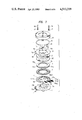
- FIG. 4 shows an automatic diaphragm unit for a lens used in cameras such as still camera, movie camera, television camera and video camera, and projectors such as movie projector and enlarger.
- cameras such as still camera, movie camera, television camera and video camera, and projectors such as movie projector and enlarger.
- projectors such as movie projector and enlarger.
- the like elements to those shown in FIG. 1 are designated by like numerals.
- Numeral 7 denotes a base, and an absorber 4, an electro-strain element 3, an insulator 50, a vibrating member 2 and a rotating member 9 which is a moving member are inserted, in this order, into a central cylinder 7a of the base 7.
- a diaphragm vane 12 is arranged thereon.
- a circular aperture 12b and an arcuate aperture 12a of the vane 12 engage with a projection 7b of the base 7 and a projection 9a of the rotating member 9, respectively, and thrust bearings 13 are positioned by spacers 14 and pressed by a pressing plate 15.
- the pressing plate 15 is pressed to the base 7 by springs 17 and they are linked together by bolts 16 to maintain an integrity of the diaphragm unit and form a portion of a lens barrel (not shown).
- the base 7 has an arcuate comb-shaped electrode 8a formed in an outer periphery, which contacts to a sliding element 8b projecting from the rotating member 9 to produce a signal in accordance with a rotation angle of the rotating member 9.
- An open reset switch SW is mounted at an end of the electrode 8a and it is actuated by a projection 9b formed on the rotating member 9.
- the absorber 4 may be made of rubber and serves to absorb the vibration of the vibrating member 2.
- the electro-strain element 3 serves as a vibration source when a voltage is applied thereto. As shown in FIG. 5A, it has two polarized portions 3a and 3b each having a plurality of polarized areas. The polarized portions 3a and 3b are physically staggered by one-quarter wavelength ( ⁇ /4). Symbols (+) and (-) show directions of polarization. In the (+) area, the element is expanded when the voltage is applied, and in the (-) area, the element is shrinks when the voltage is applied. A length determined by a sum length of the (+) area and the (-) area corresponds to one wavelength ( ⁇ ) of the input frequency. A circumference of the electro-strain element ring 3 is an integer multiple of the length determined by the sum length of the (+) area and the (-) area. In the illustrated example, it is six times as long as the sum length.
- FIG. 5(b) shows electrode patterns 3c 1 and 3d 1 on an upper surface (facing the insulator 50) of the electro-strain element 3
- FIG. 5(c) shows electrode patterns 3c 2 and 3d 2 on a lower surface (facing the absorber 4).
- the electrodes 3c 1 and 3d 1 on the upper surface are guided to the lower surface while they are insulated from each other.
- the electrodes 3c 1 and 3c 2 are disposed at the position corresponding to the polarized portion 3a, and the electrodes 3d 1 and 3d 2 are disposed at the position corresponding to the polarized portion 3b. They are connected to the lead wires on the lower surface so that the voltage is applied to the polarized portions 3a and 3b.
- the insulator 50 is inserted between the metal elastic vibrating member 2 and the electro-strain element 3 when they are bonded and serves to insulate the electrodes 3c 1 and 3d 1 of the electro-strain element 3 from each other.
- the vibration wave generated in the vibrating member 2 rotates the rotating plate 9 press-contacted to the vibrating member 2.
- the diaphragm vane 12 which engages with the projection 9a is pivotably advanced or retracted around the shafts 7b and 12b along the arcuate aperture 12a. Since the diaphragm vane 12 is provided one for each of the projections 9a (although only one vane is shown in FIG. 4), the central aperture is stopped or opened as the diaphragm vanes are pivotably advanced or retracted.
- FIG. 6 shows a control circuit for the automatic diaphragm unit described above, which is applied to a still camera of a type of exposure setting at maximum aperture.
- E denotes a power supply battery and SW 0 denotes a power switch.
- a circuit 19 including a photosensor SPC and an operational amplifier 20 is a light measurement circuit which converts a brightness of an object to an electrical signal and produces an electrical signal representing brightness information (B V ) at an output terminal.
- Potentiometers 21 and 22 constitute photographing information input means.
- film sensitivity information (S V ) and exposure information (for example, shutter time T V ) are set, the photographing information input means produces an electrical signal in accordance with the set information.
- Numeral 23 denotes an operating amplifier for determining an aperture value. The amount ⁇ A V to be stopped from the full open aperture state is given by
- a V is the aperture value to be controlled and A V0 is the full open aperture value.
- the light amount applied to the photosensor SPC that is, the output B V0 of the SPC is given by
- the number of stop steps of the automatic diaphragm unit is determined by the output ⁇ A V .
- Numeral 24 denotes an analog-to-digital converter which converts the number of stop steps signal ⁇ A V from the operational amplifier 23 to a digital signal.
- Numeral 25 denotes a pulse generator which generate a pulse each time when the slider 8b contacts the comb-shaped electrode as the rotating member 9 is rotated, by means of the slider 8b (see FIG. 4) which slides on the electrode 8a and the resistor 26.
- Numeral 27 denotes a chattering absorption circuit which eliminates a chattering component from the signal supplied from the electrode 8a connected to the power supply through the resistor 26.
- Numeral 28 denotes a circuit for controlling the stop operation by the diaphragm activation signal.
- Numeral 30 denotes a flip-flop which is set by a power supply signal C synchronized with a first step stroke of a shutter release to produce a signal ⁇ 2 and reset by a diaphragm control start signal A to produce a signal ⁇ 2 .
- Numeral 29 denotes a flip-flop which is set by the diaphragm control start signal A synchronized with a second step stroke of the shutter release to produce a signal ⁇ 1 and reset by an exposure control end signal B to produce a signal ⁇ 1 .
- Numeral 31 denotes a monostable multivibrator which produces a signal pulse of a very short duration in response to the output ⁇ 1 from the circuit 29.
- Numeral 32 denotes a presettable decrement counter which is reset by the output ⁇ 1 from the circuit 29 and preset with the output data from the analog-to-digital converter 24 in response to the output signal from the monostable multivibrator 31 triggered by the output ⁇ 1 of the circuit 29. It counts down the preset data in response to the output from the chattering absorption circuit 27 and produces a carry output when the counting is over.
- SW denotes a switch (see FIG. 4) which is closed when the diaphragm is in the open position and opened when the diaphragm vanes are stopped even slightly.
- Numeral 34 denotes a pulse generator. An output from an oscillator 37 is supplied to a frequency divider 36 and to a frequency divider 35 through a NOT circuit 43. The pulse generator 34 is triggered by the power supply signal C and produces pulses of 90° phase difference from each other.
- Numeral 38 denotes a driver for driving the polarized portions 3a and 3b of the electro-strain element. It is a push-pull circuit constructed by a plurality of transistors, resistors and NOT circuits. Numerals 39 and 40 denote switching transistors for switching the power supply to apply the voltage to the polarized portions 3a and 3b, respectively, of the electro-strain element through the push-pull circuit.
- ANDl, AND2 and AND3 denote AND circuits, OR denotes an OR circuit and EXOR denotes an exclusive OR circuit, which are known per se.
- the power switch SW 0 is turned on at the first step stroke of the shutter release and the circuits such as the light measurement and pulse generating circuit 30 are energized.
- the operational amplifier 23 calculates the diaphragm stop value ⁇ A V based on the brightness of the object, the photographing information T V and the sensitivity information S V , and the resulting ⁇ A V value is converted to a digital value by the converter 24.
- the circuit 30 is set by the signal C at the first step stroke of the shutter release and the "H" signal at the ⁇ 2 -output is supplied to the OR circuit, which produces the “H” output, which in turn closes the transistor 40.
- the "L” signal at the ⁇ 2 -output is supplied to the AND3, which produces the “L” signal, which in turn opens the transistor 39.
- the voltage is applied to the polarized portion 3b but no voltage is applied to the polarized portion 3a.
- the pulse generator 34 As the pulse generator 34 is triggered by the signal C, the output pulse from the frequency divider 36 is supplied to the push-pull circuit for the polarized portion 3b. As a result, the polarized portion 3b vibrates but the polarized portion 3a does not vibrate because no voltage is applied thereto as described above. Accordingly, a standing wave is generated in the vibrating member 2 and the rotating member 9 does not rotate but stores a vibration energy.
- the circuit 30 is reset by the diaphragm control start signal A generated at the second step stroke of the shutter release and the ⁇ 2 -output produces the "L” signal and the ⁇ 2 -output produces the "H” signal.
- the circuit 29 is set and its ⁇ 1 -output produces the "H” signal and the ⁇ 1 -output produces the "L” signal.
- the counter 32 which receives the ⁇ 1 -output at the reset terminal thereof is now released from the reset state and the counter 32 presets the digital value applied to the preset data input terminal thereof from the converter 24 in response to the output signal from the multivibrator 31 which is triggered by the ⁇ 1 -output.
- the pulse signal from the frequency divider 35 is supplied to the EXOR.
- the EXOR produces a pulse which is 90° in advance to the pulse signal from the frequency divider 36. Since the ⁇ 1 -output is also supplied to the AND2, the AND2 produces the "H” signal and the OR also produces the "H” signal, which is supplied to the AND3 and keeps the transistor 40 closed. Since the ⁇ 2 -output applied to the other input terminal of the AND3 is also the "H” signal, the AND3 produces the "H” signal and the transistor 39 is closed.
- the drive voltages having 90° phase difference are applied to the polarized portions 3a and 3b of the electro-strain element 3 to vibrate them.
- the vibrating wave is generated in the vibrating member 2 and the rotating member 9 is rotated in the direction of the arrow (see FIG. 4) so that the diaphragm vanes 12 are stopped from the open position.
- the switch SW is opened and the comb-switch 8a and 8b is repeatedly turned on and off.
- the counter 32 counts down the number of pulses corresponding to the rotation angle of the rotating member 9, supplied from the chattering absorption circuit 27 until the count reaches the preset count.
- the count of the counter 32 reaches zero, it produces the carry output or the "H” signal and the AND2 produces the "L” signal, which is supplied to the OR. Since the input to the other input terminal of the OR is also the "L” signal, the OR produces the “L” signal and the AND3 also produces the "L” signal.
- the transistors 39 and 40 are both opened and the supply of the power is stopped.
- the aperture value A V presented by the diaphragm vanes 12 is equal to a sum of the full open aperture value A V0 and the stopping aperture value ⁇ A V , that is,
- the circuit 29 When the exposure to a film is completed by the shutter operation, the circuit 29 is reset by the exposure control end signal B and the ⁇ 1 -output produces the "L” signal and the ⁇ 1 -output produces the "H” signal, which is supplied to the AND1. Since the switch SW is open, the AND1 produces the “H” signal, which is supplied to the OR. Thus, the OR produces the “H” signal which is supplied to the AND3 and closes the transistor 40. Since the ⁇ 2 -output of the circuit 30 is the “H” signal and the output of the OR is the "H” signal, the AND3 produces the "H” signal and the transistor 39 is closed. As a result, the polarized portions 3a and 3b of the electro-strain element 3 are both supplied with the power.
- the output of the frequency divider 35 is inverted by the EXOR. Accordingly, the output of the frequency divider 35 is 90° retarded to the output of the frequency divider 36.
- the rotating member 9 is rotated in the opposite direction to the arrow by the travelling vibration wave of the vibrating member 2 due to the vibration of the electro-strain element portions 3a and 3b to open the diaphragm.
- the switch SW is closed and the "L" signal is supplied to the AND1. Since the all inputs to the OR are the “L” signals, the OR produces the "L” signal which opens the transistors 39 and 40 to block the supply of power to the electro-strain element portions 3a and 3b.
- the diaphragm vanes 12 are stopped at the open position.
- the motor can be driven by the push-pull circuit driven by the single DC power supply without requiring the AC power supply. Therefore, the motor is very compact and simple and can be used in a wide range of applications.
- the insulator 50 is used in the embodiment to insulate the electrodes of the electro-strain element 3 from each other, the insulator may not be provided but the vibrating member 2 is made of aluminum and the surface thereof is almite-processed to form a ⁇ -Al 2 O 3 insulative layer to insulate the electrodes of the electro-strain element 3 from each other. Since the almite layer has a high surface hardness, the anti-abrasion property of the friction-drive surface to the moving member is enhanced.
- the vibrating member 2 may be formed of a non-conductive material having a high Young's modulus, a high surface roughness and a high surface hardness such as ceramics.
- FIG. 7 shows a modification of FIG. 4.
- the like elements to those shown in FIG. 4 are designated by the like numerals and they are not specifically explained here.
- the lower surface of the electro-strain element 3 contacts to the conductive vibration absorber 4.
- the absorber 4 is elastic and Zebra-Gome (trade name) is radially embedded in the ring for insulation. Accordingly, the absorber 4 is conductive vertically but non-conductive circumferentially. A wiring plate 51 contacts to the absorber 4.
- the wiring plate 51 is preferably flexible although it is not essential. Patterned electrodes 51c 1 , 51c 2 , 51d 1 and 51d 2 are formed on an insulative base 52.
- the electrode pattern 51c 1 faces an electrode pattern 3c 1 of the polarized portion 3a
- the electrode pattern 51c 2 faces an electrode pattern 3c 2
- the electrode pattern 51d 1 faces an electrode pattern 3d 1
- the electrode pattern 51d 2 faces an electrode pattern 3d 2 .
- Line portions of the electrodes 51c 1' , 51c 2 , 51d 1 , and 51d 2 are patterned to avoid the contact to the absorber 4 and they are connected to the push-pull circuit (see FIG. 6) of the voltage supply circuit.
- the voltage is applied to the polarized portion 3a through the electrodes 51c 1 , 3c 1 , 51c 2 and 3c 2 , and to the polarized portion 3b through the electrodes 51d 1 , 3d 1 , 51d 2 and 3d 2 .
- the lead wires need not be soldered directly to the electro-strain element 3. Accordingly, it is adapted to mass production and offers a stable quality and long life.
- the present invention can also be applied to any diaphragm unit of the lens for any camera and projector, or a drive unit for other equipment or device.
Abstract
Description
ΔA.sub.V =A.sub.V -A.sub.V0 (1)
B.sub.V0 =B.sub.V -A.sub.V0 (2)
B.sub.V +S.sub.V =A.sub.V +T.sub.V
(B.sub.V -A.sub.V0)+S.sub.V -T.sub.V =A.sub.V -A.sub.V0 =ΔA.sub.V
A.sub.V0 +ΔA.sub.V =A.sub.V
Claims (10)
Applications Claiming Priority (4)
| Application Number | Priority Date | Filing Date | Title |
|---|---|---|---|
| JP57206299A JPS5996882A (en) | 1982-11-25 | 1982-11-25 | Vibration wave motor |
| JP57206300A JPS5996883A (en) | 1982-11-25 | 1982-11-25 | Vibration wave motor |
| JP57-206300 | 1982-11-25 | ||
| JP57-206299 | 1982-11-25 |
Publications (1)
| Publication Number | Publication Date |
|---|---|
| US4513219A true US4513219A (en) | 1985-04-23 |
Family
ID=26515567
Family Applications (1)
| Application Number | Title | Priority Date | Filing Date |
|---|---|---|---|
| US06/552,373 Expired - Lifetime US4513219A (en) | 1982-11-25 | 1983-11-16 | Vibration wave motor |
Country Status (1)
| Country | Link |
|---|---|
| US (1) | US4513219A (en) |
Cited By (50)
| Publication number | Priority date | Publication date | Assignee | Title |
|---|---|---|---|---|
| US4562373A (en) * | 1983-10-21 | 1985-12-31 | Matsushita Electric Industrial Co., Ltd. | Piezoelectric motor |
| US4562374A (en) * | 1982-02-25 | 1985-12-31 | Toshiiku Sashida | Motor device utilizing ultrasonic oscillation |
| US4634916A (en) * | 1984-10-02 | 1987-01-06 | Ngk Spark Plug Co., Ltd. | Piezoelectric rotary driver |
| US4634915A (en) * | 1983-10-26 | 1987-01-06 | Canon Kabushiki Kaisha | Mount for surface wave motor |
| US4678956A (en) * | 1984-02-10 | 1987-07-07 | Canon Kabushiki Kaisha | Vibration wave motor |
| US4723085A (en) * | 1985-03-29 | 1988-02-02 | Canon Kabushiki Kaisha | Vibration wave motor |
| US4743788A (en) * | 1985-11-20 | 1988-05-10 | Nippon Kogaku K. K. | Input frequency control device for surface acoustic wave motor |
| US4743791A (en) * | 1985-11-27 | 1988-05-10 | Canon Kabushiki Kaisha | Vibration wave motor |
| US4763148A (en) * | 1986-05-09 | 1988-08-09 | Canon Kabushiki Kaisha | Vibration wave motor |
| US4779018A (en) * | 1985-10-24 | 1988-10-18 | Canon Kabushiki Kaisha | Vibration wave motor |
| US4786836A (en) * | 1984-03-01 | 1988-11-22 | Matsushita Electric Industrail Co., Ltd. | Piezoelectric motor |
| US4788468A (en) * | 1983-07-04 | 1988-11-29 | Canon Kabushiki Kaisha | Vibration wave motor |
| US4794294A (en) * | 1986-06-12 | 1988-12-27 | Canon Kabushiki Kaisha | Vibration wave motor |
| US4812699A (en) * | 1986-11-11 | 1989-03-14 | Nikon Corporation | Drive control device in an ultrasonic vibration motor |
| US4831305A (en) * | 1984-04-02 | 1989-05-16 | Canon Kabushiki Kaisha | Vibration wave motor |
| US4833359A (en) * | 1987-01-27 | 1989-05-23 | Matsushita Electric Industrial Co., Ltd. | Driving apparatus for ultrasonic motor |
| US4871937A (en) * | 1987-03-27 | 1989-10-03 | Olympus Optical Co., Ltd. | Vibration wave motor |
| WO1989011163A1 (en) * | 1988-05-11 | 1989-11-16 | Debiopharm Sa | Device for generating an elastic wave which advances along a closed trajectory |
| US4914338A (en) * | 1986-12-17 | 1990-04-03 | Canon Kabushiki Kaisha | Vibration wave motor |
| US4914337A (en) * | 1987-02-09 | 1990-04-03 | Nikon Corporation | Power supply frequency regulating device for vibration wave driven motor |
| US4926085A (en) * | 1988-05-06 | 1990-05-15 | Canon Kabushiki Kaisha | Vibration wave motor |
| US4954742A (en) * | 1988-01-11 | 1990-09-04 | Canon Kabushiki Kaisha | Vibratory-wave motor device |
| US4980597A (en) * | 1989-06-27 | 1990-12-25 | Brother Kogyo Kabushiki Kaisha | Ultrasonic motor with vibration suppressor |
| US5039899A (en) * | 1989-02-28 | 1991-08-13 | Brother Kogyo Kabushiki Kaisha | Piezoelectric transducer |
| US5061882A (en) * | 1987-02-09 | 1991-10-29 | Nikon Corporation | Power supply frequency regulating device for vibration wave driven motor |
| US5068565A (en) * | 1989-01-30 | 1991-11-26 | Huang Daxu | Motor conversion mechanism utilizing elastic action |
| US5134348A (en) * | 1989-04-07 | 1992-07-28 | Canon Kabushiki Kaisha | Vibration wave motor |
| US5136215A (en) * | 1986-12-15 | 1992-08-04 | Canon Kabushiki Kaisha | Driving circuit for vibration wave motor |
| US5229678A (en) * | 1989-10-20 | 1993-07-20 | Seiko Epson Corporation | Drive control unit for an ultrasonic step motor |
| US5237237A (en) * | 1990-03-12 | 1993-08-17 | Seiko Epson Corporation | Ultrasonic motor and drive method |
| US5247220A (en) * | 1989-10-20 | 1993-09-21 | Seiko Epson Corporation | Ultrasonic motor |
| USRE34409E (en) * | 1983-05-04 | 1993-10-19 | Nikon Corporation | Drive circuit for surface-wave driven motor utilizing ultrasonic vibration |
| US5448127A (en) * | 1990-05-15 | 1995-09-05 | Canon Kabushiki Kaisha | Vibration wave driven motor |
| US5471108A (en) * | 1993-02-05 | 1995-11-28 | Imra Europe Sa And Techsonic | Realization process of a distribution network of electric signals, obtained distribution network and piezoelectric motor including such a network |
| US5479380A (en) * | 1989-10-20 | 1995-12-26 | Seiko Epson Corporation | Ultrasonic motor for driving an analog electronic watch |
| US5540615A (en) * | 1994-05-19 | 1996-07-30 | The Regents Of The University Of Michigan | Machine balancer |
| US5648696A (en) * | 1993-08-18 | 1997-07-15 | Figest B.V. | Piezoelectric motor with progressive wave |
| US5945769A (en) * | 1991-08-26 | 1999-08-31 | Canon Kabushiki Kaisha | Wave driven motor |
| US6051911A (en) * | 1993-12-27 | 2000-04-18 | Canon Kabushiki Kaisha | Vibration wave actuator |
| US6262515B1 (en) | 2000-02-18 | 2001-07-17 | Honeywell International, Inc. | Piezoelectric wave motor |
| US6467139B1 (en) | 1998-08-03 | 2002-10-22 | Nec Corporation | Mounting structure and mounting method for surface acoustic wave element |
| US6518689B2 (en) | 2000-02-18 | 2003-02-11 | Honeywell Federal Manufacturing & Technologies, Llc | Piezoelectric wave motor |
| US6727635B2 (en) * | 2000-09-11 | 2004-04-27 | Minolta Co., Ltd. | Driving device |
| US20050008168A1 (en) * | 2001-10-09 | 2005-01-13 | Pompei Frank Joseph | Ultrasonic transducer for parametric array |
| US20060290234A1 (en) * | 2005-06-23 | 2006-12-28 | Olympus Corporation | Driving method for ultrasonic motor and apparatus using the same |
| US7215062B1 (en) * | 1998-08-07 | 2007-05-08 | Seiko Instruments Inc. | Ultrasonic motor and electronic appliance with ultrasonic motor |
| US20080054760A1 (en) * | 2006-09-05 | 2008-03-06 | Canon Kabushiki Kaisha | Vibration control apparatus and method |
| US7671516B2 (en) | 2005-12-05 | 2010-03-02 | Panasonic Corporation | Ultrasonic actuator |
| US20110133602A1 (en) * | 2009-12-04 | 2011-06-09 | Samsung Electronics Co., Ltd. | Piezoelectric motor |
| US10211760B2 (en) | 2015-05-15 | 2019-02-19 | Samsung Electronics Co., Ltd. | Piezoelectric ultrasonic motor and operation method of the same |
Citations (7)
| Publication number | Priority date | Publication date | Assignee | Title |
|---|---|---|---|---|
| US3389274A (en) * | 1965-12-06 | 1968-06-18 | Perkin Elmer Corp | Peristaltic actuator |
| US3649856A (en) * | 1970-08-03 | 1972-03-14 | Physics Int Co | Transducer for converting digital signals into linear motion |
| US4019073A (en) * | 1975-08-12 | 1977-04-19 | Vladimir Sergeevich Vishnevsky | Piezoelectric motor structures |
| SU573828A1 (en) * | 1976-06-08 | 1977-09-25 | Киевский Ордена Ленина Политехнический Институт Имени 50-Летия Великой Октябрьской Социалистической Революции | Piezoelectric motor |
| SU612357A1 (en) * | 1975-11-06 | 1978-06-25 | Abramov Valentin A | Wave-type electric motor |
| SU646395A1 (en) * | 1978-01-26 | 1979-02-05 | Каунасский Политехнический Институт Им. Антанаса Снечкуса | Synchronous vibrodrive |
| US4400641A (en) * | 1982-04-16 | 1983-08-23 | Kievsky Politekhnichesky Institut | Piezoelectric motor with two part rotor |
-
1983
- 1983-11-16 US US06/552,373 patent/US4513219A/en not_active Expired - Lifetime
Patent Citations (7)
| Publication number | Priority date | Publication date | Assignee | Title |
|---|---|---|---|---|
| US3389274A (en) * | 1965-12-06 | 1968-06-18 | Perkin Elmer Corp | Peristaltic actuator |
| US3649856A (en) * | 1970-08-03 | 1972-03-14 | Physics Int Co | Transducer for converting digital signals into linear motion |
| US4019073A (en) * | 1975-08-12 | 1977-04-19 | Vladimir Sergeevich Vishnevsky | Piezoelectric motor structures |
| SU612357A1 (en) * | 1975-11-06 | 1978-06-25 | Abramov Valentin A | Wave-type electric motor |
| SU573828A1 (en) * | 1976-06-08 | 1977-09-25 | Киевский Ордена Ленина Политехнический Институт Имени 50-Летия Великой Октябрьской Социалистической Революции | Piezoelectric motor |
| SU646395A1 (en) * | 1978-01-26 | 1979-02-05 | Каунасский Политехнический Институт Им. Антанаса Снечкуса | Synchronous vibrodrive |
| US4400641A (en) * | 1982-04-16 | 1983-08-23 | Kievsky Politekhnichesky Institut | Piezoelectric motor with two part rotor |
Cited By (63)
| Publication number | Priority date | Publication date | Assignee | Title |
|---|---|---|---|---|
| US4562374A (en) * | 1982-02-25 | 1985-12-31 | Toshiiku Sashida | Motor device utilizing ultrasonic oscillation |
| USRE33390E (en) * | 1982-02-25 | 1990-10-16 | Motor device utilizing ultrasonic oscillation | |
| USRE34409E (en) * | 1983-05-04 | 1993-10-19 | Nikon Corporation | Drive circuit for surface-wave driven motor utilizing ultrasonic vibration |
| US4788468A (en) * | 1983-07-04 | 1988-11-29 | Canon Kabushiki Kaisha | Vibration wave motor |
| US4562373A (en) * | 1983-10-21 | 1985-12-31 | Matsushita Electric Industrial Co., Ltd. | Piezoelectric motor |
| US4634915A (en) * | 1983-10-26 | 1987-01-06 | Canon Kabushiki Kaisha | Mount for surface wave motor |
| US4678956A (en) * | 1984-02-10 | 1987-07-07 | Canon Kabushiki Kaisha | Vibration wave motor |
| US4786836A (en) * | 1984-03-01 | 1988-11-22 | Matsushita Electric Industrail Co., Ltd. | Piezoelectric motor |
| US4831305A (en) * | 1984-04-02 | 1989-05-16 | Canon Kabushiki Kaisha | Vibration wave motor |
| US4634916A (en) * | 1984-10-02 | 1987-01-06 | Ngk Spark Plug Co., Ltd. | Piezoelectric rotary driver |
| US4723085A (en) * | 1985-03-29 | 1988-02-02 | Canon Kabushiki Kaisha | Vibration wave motor |
| US4779018A (en) * | 1985-10-24 | 1988-10-18 | Canon Kabushiki Kaisha | Vibration wave motor |
| US4743788A (en) * | 1985-11-20 | 1988-05-10 | Nippon Kogaku K. K. | Input frequency control device for surface acoustic wave motor |
| US4743791A (en) * | 1985-11-27 | 1988-05-10 | Canon Kabushiki Kaisha | Vibration wave motor |
| US4763148A (en) * | 1986-05-09 | 1988-08-09 | Canon Kabushiki Kaisha | Vibration wave motor |
| US4794294A (en) * | 1986-06-12 | 1988-12-27 | Canon Kabushiki Kaisha | Vibration wave motor |
| US4812699A (en) * | 1986-11-11 | 1989-03-14 | Nikon Corporation | Drive control device in an ultrasonic vibration motor |
| US5136215A (en) * | 1986-12-15 | 1992-08-04 | Canon Kabushiki Kaisha | Driving circuit for vibration wave motor |
| US4914338A (en) * | 1986-12-17 | 1990-04-03 | Canon Kabushiki Kaisha | Vibration wave motor |
| US4833359A (en) * | 1987-01-27 | 1989-05-23 | Matsushita Electric Industrial Co., Ltd. | Driving apparatus for ultrasonic motor |
| USRE35852E (en) * | 1987-02-09 | 1998-07-21 | Nikon Corporation | Power supply frequency regulating device for vibration wave driven motor |
| US4914337A (en) * | 1987-02-09 | 1990-04-03 | Nikon Corporation | Power supply frequency regulating device for vibration wave driven motor |
| US5061882A (en) * | 1987-02-09 | 1991-10-29 | Nikon Corporation | Power supply frequency regulating device for vibration wave driven motor |
| US4871937A (en) * | 1987-03-27 | 1989-10-03 | Olympus Optical Co., Ltd. | Vibration wave motor |
| US4918351A (en) * | 1987-03-27 | 1990-04-17 | Olympus Optical Co. | Vibration wave motor |
| US4954742A (en) * | 1988-01-11 | 1990-09-04 | Canon Kabushiki Kaisha | Vibratory-wave motor device |
| US4926085A (en) * | 1988-05-06 | 1990-05-15 | Canon Kabushiki Kaisha | Vibration wave motor |
| WO1989011163A1 (en) * | 1988-05-11 | 1989-11-16 | Debiopharm Sa | Device for generating an elastic wave which advances along a closed trajectory |
| US5068565A (en) * | 1989-01-30 | 1991-11-26 | Huang Daxu | Motor conversion mechanism utilizing elastic action |
| US5039899A (en) * | 1989-02-28 | 1991-08-13 | Brother Kogyo Kabushiki Kaisha | Piezoelectric transducer |
| US5134348A (en) * | 1989-04-07 | 1992-07-28 | Canon Kabushiki Kaisha | Vibration wave motor |
| US4980597A (en) * | 1989-06-27 | 1990-12-25 | Brother Kogyo Kabushiki Kaisha | Ultrasonic motor with vibration suppressor |
| US5229678A (en) * | 1989-10-20 | 1993-07-20 | Seiko Epson Corporation | Drive control unit for an ultrasonic step motor |
| US5521455A (en) * | 1989-10-20 | 1996-05-28 | Seiko Epson Corporation | Ultrasonic motor |
| US5247220A (en) * | 1989-10-20 | 1993-09-21 | Seiko Epson Corporation | Ultrasonic motor |
| US5479380A (en) * | 1989-10-20 | 1995-12-26 | Seiko Epson Corporation | Ultrasonic motor for driving an analog electronic watch |
| US5237237A (en) * | 1990-03-12 | 1993-08-17 | Seiko Epson Corporation | Ultrasonic motor and drive method |
| US5632074A (en) * | 1990-05-15 | 1997-05-27 | Canon Kabushiki Kaisha | Vibration wave driven motor |
| US5448127A (en) * | 1990-05-15 | 1995-09-05 | Canon Kabushiki Kaisha | Vibration wave driven motor |
| US5945769A (en) * | 1991-08-26 | 1999-08-31 | Canon Kabushiki Kaisha | Wave driven motor |
| US5471108A (en) * | 1993-02-05 | 1995-11-28 | Imra Europe Sa And Techsonic | Realization process of a distribution network of electric signals, obtained distribution network and piezoelectric motor including such a network |
| US5648696A (en) * | 1993-08-18 | 1997-07-15 | Figest B.V. | Piezoelectric motor with progressive wave |
| US6051911A (en) * | 1993-12-27 | 2000-04-18 | Canon Kabushiki Kaisha | Vibration wave actuator |
| US5540615A (en) * | 1994-05-19 | 1996-07-30 | The Regents Of The University Of Michigan | Machine balancer |
| US6467139B1 (en) | 1998-08-03 | 2002-10-22 | Nec Corporation | Mounting structure and mounting method for surface acoustic wave element |
| US7215062B1 (en) * | 1998-08-07 | 2007-05-08 | Seiko Instruments Inc. | Ultrasonic motor and electronic appliance with ultrasonic motor |
| US6262515B1 (en) | 2000-02-18 | 2001-07-17 | Honeywell International, Inc. | Piezoelectric wave motor |
| US6518689B2 (en) | 2000-02-18 | 2003-02-11 | Honeywell Federal Manufacturing & Technologies, Llc | Piezoelectric wave motor |
| US6727635B2 (en) * | 2000-09-11 | 2004-04-27 | Minolta Co., Ltd. | Driving device |
| US20100158285A1 (en) * | 2001-10-09 | 2010-06-24 | Frank Joseph Pompei | Ultrasonic transducer for parametric array |
| US20050008168A1 (en) * | 2001-10-09 | 2005-01-13 | Pompei Frank Joseph | Ultrasonic transducer for parametric array |
| US8472651B2 (en) | 2001-10-09 | 2013-06-25 | Frank Joseph Pompei | Ultrasonic transducer for parametric array |
| US8369546B2 (en) | 2001-10-09 | 2013-02-05 | Frank Joseph Pompei | Ultrasonic transducer for parametric array |
| US7657044B2 (en) * | 2001-10-09 | 2010-02-02 | Frank Joseph Pompei | Ultrasonic transducer for parametric array |
| US20100158286A1 (en) * | 2001-10-09 | 2010-06-24 | Frank Joseph Pompei | Ultrasonic transducer for parametric array |
| US7449814B2 (en) * | 2005-06-23 | 2008-11-11 | Olympus Corporation | Driving method for ultrasonic motor and apparatus using the same |
| US20060290234A1 (en) * | 2005-06-23 | 2006-12-28 | Olympus Corporation | Driving method for ultrasonic motor and apparatus using the same |
| US7671516B2 (en) | 2005-12-05 | 2010-03-02 | Panasonic Corporation | Ultrasonic actuator |
| US7608980B2 (en) * | 2006-09-05 | 2009-10-27 | Canon Kabushiki Kaisha | Vibration control apparatus and method |
| US20080054760A1 (en) * | 2006-09-05 | 2008-03-06 | Canon Kabushiki Kaisha | Vibration control apparatus and method |
| US20110133602A1 (en) * | 2009-12-04 | 2011-06-09 | Samsung Electronics Co., Ltd. | Piezoelectric motor |
| US8643251B2 (en) | 2009-12-04 | 2014-02-04 | Samsung Electronics Co., Ltd. | Piezoelectric motor having a plurality of piezoelectric elements |
| US10211760B2 (en) | 2015-05-15 | 2019-02-19 | Samsung Electronics Co., Ltd. | Piezoelectric ultrasonic motor and operation method of the same |
Similar Documents
| Publication | Publication Date | Title |
|---|---|---|
| US4513219A (en) | Vibration wave motor | |
| US4560263A (en) | Drive system for a vibration wave motor for lens control | |
| US4495432A (en) | Piezoelectric vibration wave motor with sloped drive surface | |
| US4491401A (en) | Diaphragm device | |
| US4504760A (en) | Piezoelectrically driven vibration wave motor | |
| US4660933A (en) | Lens driving device | |
| US5402030A (en) | Vibration wave driven apparatus | |
| JPH041598B2 (en) | ||
| US5669127A (en) | Method of manufacturing an electro-mechanical energy conversion device for vibration driven actuator | |
| JPH07170772A (en) | Ultrasonic motor and electronic equipment with ultrasonic motor | |
| US4755705A (en) | Piezoelectric motor | |
| JPH04145881A (en) | Ultrasonic motor | |
| JPH0472470B2 (en) | ||
| JPH0514510B2 (en) | ||
| US5798598A (en) | Vibration driven device | |
| JPH0474952B2 (en) | ||
| US4888515A (en) | Rotary power unit | |
| JPH08251949A (en) | Oscillation driver | |
| JPH0466007B2 (en) | ||
| JPH0410607B2 (en) | ||
| JPS62260567A (en) | Oscillatory wave motor | |
| JPH04211210A (en) | Lens barrel by use of vibrating motor | |
| JPS59106886A (en) | Drive system for vibration wave motor | |
| JPH112752A (en) | Vibration actuator driving device and lens barrel | |
| JPS59197026A (en) | Electrically driven camera using oscillatory wave motor |
Legal Events
| Date | Code | Title | Description |
|---|---|---|---|
| AS | Assignment |
Owner name: CANON KABUSHIKI KAISHA 30-2 3 CHOME SHIMOMAURKO OH Free format text: ASSIGNMENT OF ASSIGNORS INTEREST.;ASSIGNORS:KATSUMA, MAKOTO;MURAKAMI, HIROYASU;HIRAMATSU, AKIRA;REEL/FRAME:004198/0860 Effective date: 19831114 Owner name: CANON KABUSHIKI KAISHA 30-2 3 CHOME SHIMOMAURKO OH Free format text: ASSIGNMENT OF ASSIGNORS INTEREST;ASSIGNORS:KATSUMA, MAKOTO;MURAKAMI, HIROYASU;HIRAMATSU, AKIRA;REEL/FRAME:004198/0860 Effective date: 19831114 |
|
| STCF | Information on status: patent grant |
Free format text: PATENTED CASE |
|
| CC | Certificate of correction | ||
| FPAY | Fee payment |
Year of fee payment: 4 |
|
| FPAY | Fee payment |
Year of fee payment: 8 |
|
| FPAY | Fee payment |
Year of fee payment: 12 |