US4525730A - Buried junction Josephson interferometer - Google Patents
Buried junction Josephson interferometer Download PDFInfo
- Publication number
- US4525730A US4525730A US06/445,331 US44533182A US4525730A US 4525730 A US4525730 A US 4525730A US 44533182 A US44533182 A US 44533182A US 4525730 A US4525730 A US 4525730A
- Authority
- US
- United States
- Prior art keywords
- interferometer
- counter
- electrodes
- bridge
- base electrode
- Prior art date
- Legal status (The legal status is an assumption and is not a legal conclusion. Google has not performed a legal analysis and makes no representation as to the accuracy of the status listed.)
- Expired - Fee Related
Links
Images

Classifications
-
- H—ELECTRICITY
- H10—SEMICONDUCTOR DEVICES; ELECTRIC SOLID-STATE DEVICES NOT OTHERWISE PROVIDED FOR
- H10N—ELECTRIC SOLID-STATE DEVICES NOT OTHERWISE PROVIDED FOR
- H10N60/00—Superconducting devices
- H10N60/10—Junction-based devices
- H10N60/12—Josephson-effect devices
-
- Y—GENERAL TAGGING OF NEW TECHNOLOGICAL DEVELOPMENTS; GENERAL TAGGING OF CROSS-SECTIONAL TECHNOLOGIES SPANNING OVER SEVERAL SECTIONS OF THE IPC; TECHNICAL SUBJECTS COVERED BY FORMER USPC CROSS-REFERENCE ART COLLECTIONS [XRACs] AND DIGESTS
- Y10—TECHNICAL SUBJECTS COVERED BY FORMER USPC
- Y10S—TECHNICAL SUBJECTS COVERED BY FORMER USPC CROSS-REFERENCE ART COLLECTIONS [XRACs] AND DIGESTS
- Y10S505/00—Superconductor technology: apparatus, material, process
- Y10S505/825—Apparatus per se, device per se, or process of making or operating same
- Y10S505/873—Active solid-state device
- Y10S505/874—Active solid-state device with josephson junction, e.g. squid
Definitions
- the invention relates to superconducting logic circuits, and particularly concerns a buried junction Josephson interferometer comprising a base electrode common to the junctions and covered, at least in the junction areas, with a tunnel barrier layer on which counter-electrodes are deposited, these being connected via an interferometer bridge separated from the underlaying base electrode by an insulating layer.
- Josephson interferometers are well known in the art. In the data processing field their application has been suggested particularly for memory cells but also for logic circuitry of a wide variety of layouts and functions. The publications listed below are representative of the current state of the art:
- interferometers disclosed in these publications comprise two, three or even more Josephson junctions capable of supporting Josephson tunnel currents. These interferometers employ planar Josephson junctions formed by depositing, onto a substrate, a first layer of a metallic film of superconducting material which serves as base electrode, by a subsequent oxidation whereby the tunnel barrier is produced, and by depositing a second superconducting metallic layer, the counter-electrode. Interferometers with junctions having a common base electrode and in which the counterelectrodes are connected via a bridge, separated from the common base electrode by an insulation layer, are referred to as bridge interferometers. Their gate or threshold characteristic provides for margins and operating windows that result in a good yield. One of the essential parameters determining this characteristic is the LI o product of the interferometer structure, L being the interferometer loop inductance, I o being the maximum Josephson junction current which is proportional to the maximum current density of the junctions and to the junction area.
- L has been increased by either increasing the thickness of the insulation layers separating the bridge from the base electrode or by increasing the length of the device.
- the accomplished improvement with the first approach is limited by the planar technology used in that very thick layers provide problems when further layers have to be deposited on top of the thick layer.
- the second approach automatically leads to larger structures, i.e., to an undesired increase in the area required by the interferometer.
- the maximum Josephson current I o can be increased by increasing the current density j max . This is possible within certain limits but, above approx. 5 KA/cm 2 , becomes critical because of its effect on the switching characteristics of the interferometer. This is of particular importance in applications in single flux quantum (SFQ) vortex memory cells where stored binary values "1" and "0", respectively, are represented by the presence or absence of a flux quantum captured in the interferometer.
- SFQ single flux quantum
- a high current density results in a higher "critical point" of the threshold characteristic of the interferometer, this being the point on the vortex threshold curves above which crossing of the curves causes switching into the voltage state whereas crossing the curves below the critical point results in a change in the vortex mode, i.e., either in the capture or release of a flux quantum.
- critical point the point on the vortex threshold curves above which crossing of the curves causes switching into the voltage state whereas crossing the curves below the critical point results in a change in the vortex mode, i.e., either in the capture or release of a flux quantum.
- the interferometer herein described is characterized in that the insulating layer extends between the counter-electrodes and the interferometer bridge such that the junctions are located underneath the interferometer bridge.
- the disclosed interferometer structure provides for a higher inductance without increasing the device area and thus permits higher packaging densities than achievable with hitherto known interferometer structures. This is achieved without negatively effecting the essential characteristics of the basic interferometer such as switching speed and operating margins. It can, furthermore, be produced in a production process involving only steps that can be easily controlled.
- FIG. 1 is a schematic sectional view of a 2-Josephson-junction bridge interferometer representative of the state of the art.
- FIG. 2 is a schematic sectional view of a 2-Josephson-junction bridge interferometer in accordance with the present invention.
- FIG. 3 is a sectional view of a 2-junction interferometer structure suitable for production processes involving optical lithography steps.
- FIG. 4 is a sectional view of another 2-junction interferometer structure suitable for production processes involving optical and e-beam lithography steps.
- FIG. 5 is a sectional view of a 3-junction interferometer in accordance with the present invention.
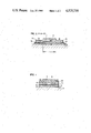
- FIG. 2 represents a schematic view of a 2-junction interferometer representative of the state of the art in which, for reasons of simplicity, only the major functional elements such as electrodes and insulations are shown. Insulations encapsulating the device as well as control lines that may be arranged on top of the interferometer structure are omitted.
- a substrate possibly covered with an insulation layer, not shown, is designated 1.
- a thin metal layer 2 of superconducting material forming the common base electrode for two Josephson junctions 3A and 3B. These are formed by the base electrode, oxide layers 4A and 4B, and by metallic superconducting counter electrodes 5A and 5B, respectively.
- Layers 4A and 4B normally consisting of an oxide of the base electrode material, are capable of supporting Josephson tunnel currents therethrough and will be referred to as tunnel barrier layers.
- the two counterelectrodes are connected via a superconducting bridge 6 which is separated from the base electrode layer 2 by insulating layer 7.
- the interferometer inductance L is essentially determined by the thickness d and the length l (between the two electrodes) of layer 7. Performance requirements often define the minimum value of the LI o product of the interferometer. With a given I o , determined by the maximum current density j max and by the junction dimensions, the area covered by the interferometer structure shown in FIG. 1 depends largely on the required value of the inductance L which is proportional to the length l. External connection to base electrode and counter-electrode may be made externally in conventional fashion.
- FIG. 1 shows a schematic view of the interferometer of the present invention.
- the new structure permits a substantial reduction of the area required for the interferometer without effecting parameters L and I o .
- the common base electrode 12 is again arranged on a substrate 11.
- the two Josephson junctions 13A and 13B are formed by this base electrode 12, the two tunnel barrier layers 14A and 14B, and by counter-electrodes 15A and 15B. These are connected via bridge 16 which, in turn, is isolated from the base electrode 12 and from the top surfaces of electrodes 15A and 15B by means of insulation 17.
- the basic concept on which this structure is based is to "bury" the Josephson junctions under the interferometer bridge.
- the counterelectrodes of the junctions become part of the inductance loop between the junctions.
- the inductance L of the interferometer of FIG. 1 is essentially determined by the length of the average thickness of the insulation layer 17.
- the inductances L are approx. the same for both interferometers.
- the LI o product is the same for both structures. Since the length of the structure of FIG. 1 and thus the required device area is reduced, the described inventive interferometer permits substantially higher packaging densities.
- FIG. 3 is a typical embodiment of the present invention. It basically corresponds to the structure briefly described with the aid of FIG. 2. All processes used to evaporate, to etch, to clean, or to "pattern" are well known and can be performed by employing conventionally available equipment. They are, therefore, not explained in greater detail here.
- a planar substrate 20 which is covered with an insulating layer 21 (FIG. 3).
- a Nb layer 22 of 2500 ⁇ thickness is evaporated onto insulation layer 21.
- Layer 22 forms the common base electrode of the interferometer.
- the desired pattern is obtained by applying well known photo-resist techniques and subsequent plasma etching.
- Insulations 23 are formed by evaporating a 500 ⁇ SiO layer onto layer 22. It is patterned in a photoresist and subsequent lift-off process resulting in the two outer sections isolating the edges of the base electrode 22 and in the center section which serves to separate the later formed barrier layers 24.
- the three insulation sections 23 determine the junction areas of the two Josephson junctions of the interferometer.
- This step is followed by a conventional rf-cleaning operation performed in order properly to condition the surface of the base electrode 22 for the next or fourth step in which the tunnel barriers 24 are obtained in a rf-oxidation process during which a Nb oxide layer (Nb 2 O 5 ) of 20 to 30 ⁇ thickness is formed on the sections of the base electrode that are not covered by the insulation 23.
- a 1000 ⁇ layer 25 of Pb alloy e.g. PbInAu
- the resulting pattern leaves a window above the center section of insulation 23.
- SiO insulation layer 26 of 2000 ⁇ thickness is deposited and shaped as shown in FIG. 3.
- planar dimensions of the interferometer structure of FIG. 3 can be chosen as follows:
- TABLE II lists the process steps required to produce the interferometer structure shown in FIG. 4 which, again, is a typical example of the present invention.
- This structure requires, for the lithography, precise alignment tools such as those employing e-beams or x-rays. These tools permit sufficiently accurate pattern definition, e.g., of the junction areas, thereby eliminating the need for the insulation layer 23 used in the structure of FIG. 3 to accurately define the junctions.
- a Nb layer 32 of 2500 ⁇ thickness is evaporated onto insulation layer 31.
- Layer 32 forms the common base electrode of the interferometer.
- the desired pattern is obtained through photo-resist techniques and subsequent plasma etching. While the resist is still on the top of the base electrode layer, edges 33 are isolated in an rf- or plasma oxidation process.
- the thickness of this Nb 2 O 5 oxidation is in the order of a few hundred ⁇ , e.g., 400 ⁇ .
- This step is followed by a conventional rf-cleaning operation.
- the tunnel barrier layers 34 are obtained in an rf-oxidation process during which the Nb oxide layer (Nb 2 O 5 ) of 20 to 30 ⁇ thickness is formed.
- a 3000 ⁇ layer 35 of Pb alloy e.g., PbInAu
- PbInAu e.g., PbInAu
- the desired pattern i.e., the definition of the junction areas, is obtained by using an e-beam produced resist stencil and a lift-off operation to accurately control the distance between the two counter-electrodes.
- a SiO insulation layer 36 of 4000 ⁇ thickness is evaporated.
- planar dimensions of the interferometer of FIG. 4 can be chosen to be
- Table III the interferometer area reduction that can be achieved with the present invention is illustrated.
- the figures apply for a 2.5 ⁇ m min. line width technology with a lithographic square of 2.5 ⁇ 2.5 ⁇ m.
- FIG. 5 is a schematic view of an asymmetric 3-junction interferometer employing the inventive concept.
- the center junction (40B) area is twice as large as that of the two outer junctions (40A, 40C).
- the base electrode common to all three junctions, is designated 41.
- the three barrier layers 42A, 42B, and 42C are separated from each other and defined by insulation layers 43A and 43B.
- Counter-electrodes 44A, 44B and 44C connect via bridge 45.
- Insulations 46AB and 46BC determine, together with the bridge and the respective counter-electrodes and base electrode sections, the inductances of the two interferometer loops.
- the Josephson junctions are placed under the interferometer bridge whereby the counter-electrodes of the junctions become part of the inductance loop between the junctions.
- the device described hereinabove is well suited for a wide variety of applications. It can, e.g., be used as basic switching element employed in logic circuitry such as that disclosed in an article by H. Beha "Asymmetric 2-Josephson-Junction Interferometer as a Logic Gate” (Electronics Letters, Mar. 31, 77, Vol. 13, No. 7, pp. 218-220).
- a 3-junction interferometer for applications in logic circuitry has been disclosed in a paper by H. Beha and H. Jackel “High Tolerance 3-Josephson Junction Current-Injection Logic Devices" (Digest of IEEE Intermag Conference 1981, Grenoble, May 12-15, 81, page 40-4).
- control currents may be magnetically coupled to the interferometer or directly injected.
- the interferometer may be symmetric or asymmetric. Obviously, different materials, dimensions or production processes may be used in making the interferometer without departing from the inventive concept.
Abstract
Planar junction Josephson interferometer in which the junctions (24) are "buried" underneath the interferometer bridge (27) connecting the junction counter-electrodes (25). The insulation (26) that separates the common base electrode (22) from the bridge (27) is extended between the bridge and the upper surfaces of the counter-electrodes. This design permits, without decreasing the interferometer loop inductance, a reduction of the interferometer area and thus results in a higher packaging density in logic or memory applications.
The buried junction concept can be applied in symmetric or asymmetric interferometer designs with virtually any number of junctions, any type of input current control or current feeding scheme.
The interferometer can be produced using conventional evaporation, photo-resist, and etch processes based on optical lithography. Further area reduction is achieved in applying e-beam or x-ray technology.
Description
This application claims priority under the International Convention for the Protection of Industrial Property, from European patent application Ser. No. 8,110,078.3, filed Dec. 2, 1981 in the European Patent Office.
The invention relates to superconducting logic circuits, and particularly concerns a buried junction Josephson interferometer comprising a base electrode common to the junctions and covered, at least in the junction areas, with a tunnel barrier layer on which counter-electrodes are deposited, these being connected via an interferometer bridge separated from the underlaying base electrode by an insulating layer.
Josephson interferometers are well known in the art. In the data processing field their application has been suggested particularly for memory cells but also for logic circuitry of a wide variety of layouts and functions. The publications listed below are representative of the current state of the art:
U.S. Pat. No. 3,936,809, Zappe, "Single Flux Quantum Storage Devices and Sensing Means Therefor," Feb. 3, 1976
Henkels, "Compact Bridge Josephson Interferometer," IBM Technical Disclosure Bulletin, Vol. 22, No. 7, December 79, pp. 2970-73.
Faris, "Coupling Element for Josephson Read-Only Memory," IBM Technical Disclosure Bulletin, Vol. 20, No. 10, March 78, pp. 4197-98.
Gheewala et al, "New Interferometer Structures," IBM Technical Disclosure Bulletin, Vol. 22, No. 5, October 79, pp. 2139-42.
Gueret et al, IEEE Transactions of Magnetics, Vol. MAG-13, No. 1, January 77, pp. 52-55, Article "Single Flux-Quantum Memory Cells." and
Gheewala, IBM Journal of Research and Development, Vol. 24, No. 2, March 1980, pp. 131-142, Article "Design of 2,5 micrometer Josephson Current Injection Logic."
The interferometers disclosed in these publications comprise two, three or even more Josephson junctions capable of supporting Josephson tunnel currents. These interferometers employ planar Josephson junctions formed by depositing, onto a substrate, a first layer of a metallic film of superconducting material which serves as base electrode, by a subsequent oxidation whereby the tunnel barrier is produced, and by depositing a second superconducting metallic layer, the counter-electrode. Interferometers with junctions having a common base electrode and in which the counterelectrodes are connected via a bridge, separated from the common base electrode by an insulation layer, are referred to as bridge interferometers. Their gate or threshold characteristic provides for margins and operating windows that result in a good yield. One of the essential parameters determining this characteristic is the LIo product of the interferometer structure, L being the interferometer loop inductance, Io being the maximum Josephson junction current which is proportional to the maximum current density of the junctions and to the junction area.
Various measures have in the past been taken to improve, i.e., to increase the LIo product. L has been increased by either increasing the thickness of the insulation layers separating the bridge from the base electrode or by increasing the length of the device. The accomplished improvement with the first approach is limited by the planar technology used in that very thick layers provide problems when further layers have to be deposited on top of the thick layer. The second approach automatically leads to larger structures, i.e., to an undesired increase in the area required by the interferometer.
On the other hand, the maximum Josephson current Io can be increased by increasing the current density jmax. This is possible within certain limits but, above approx. 5 KA/cm2, becomes critical because of its effect on the switching characteristics of the interferometer. This is of particular importance in applications in single flux quantum (SFQ) vortex memory cells where stored binary values "1" and "0", respectively, are represented by the presence or absence of a flux quantum captured in the interferometer. A high current density results in a higher "critical point" of the threshold characteristic of the interferometer, this being the point on the vortex threshold curves above which crossing of the curves causes switching into the voltage state whereas crossing the curves below the critical point results in a change in the vortex mode, i.e., either in the capture or release of a flux quantum. For memory applications, a low critical point is therefore an essential requirement for reliable switching operations and sufficiently large operating margins.
It is a main object of the present invention to provide an interferometer structure requiring a reduced area thereby permitting higher packaging densities. Another object is to present an interferometer structure permitting, without increasing the required area for the device, a layout resulting in a higher interferometer inductance thereby improving the switching characteristics of the interferometer. A further object is to provide an interferometer structure with improved characteristics that can be manufactured using well known and controllable process steps.
These objects are met by the interferometer herein described that is characterized in that the insulating layer extends between the counter-electrodes and the interferometer bridge such that the junctions are located underneath the interferometer bridge.
The disclosed interferometer structure provides for a higher inductance without increasing the device area and thus permits higher packaging densities than achievable with hitherto known interferometer structures. This is achieved without negatively effecting the essential characteristics of the basic interferometer such as switching speed and operating margins. It can, furthermore, be produced in a production process involving only steps that can be easily controlled.
Several ways of carrying out the invention are described in detail below with reference to drawings which illustrate specific embodiments, and in which
FIG. 1 is a schematic sectional view of a 2-Josephson-junction bridge interferometer representative of the state of the art.
FIG. 2 is a schematic sectional view of a 2-Josephson-junction bridge interferometer in accordance with the present invention.
FIG. 3 is a sectional view of a 2-junction interferometer structure suitable for production processes involving optical lithography steps.
FIG. 4 is a sectional view of another 2-junction interferometer structure suitable for production processes involving optical and e-beam lithography steps.
FIG. 5 is a sectional view of a 3-junction interferometer in accordance with the present invention.
FIG. 2 represents a schematic view of a 2-junction interferometer representative of the state of the art in which, for reasons of simplicity, only the major functional elements such as electrodes and insulations are shown. Insulations encapsulating the device as well as control lines that may be arranged on top of the interferometer structure are omitted.
A substrate, possibly covered with an insulation layer, not shown, is designated 1. Deposited onto this substrate is a thin metal layer 2 of superconducting material forming the common base electrode for two Josephson junctions 3A and 3B. These are formed by the base electrode, oxide layers 4A and 4B, and by metallic superconducting counter electrodes 5A and 5B, respectively. Layers 4A and 4B, normally consisting of an oxide of the base electrode material, are capable of supporting Josephson tunnel currents therethrough and will be referred to as tunnel barrier layers. The two counterelectrodes are connected via a superconducting bridge 6 which is separated from the base electrode layer 2 by insulating layer 7. The interferometer inductance L is essentially determined by the thickness d and the length l (between the two electrodes) of layer 7. Performance requirements often define the minimum value of the LIo product of the interferometer. With a given Io, determined by the maximum current density jmax and by the junction dimensions, the area covered by the interferometer structure shown in FIG. 1 depends largely on the required value of the inductance L which is proportional to the length l. External connection to base electrode and counter-electrode may be made externally in conventional fashion.
FIG. 1 shows a schematic view of the interferometer of the present invention. The new structure permits a substantial reduction of the area required for the interferometer without effecting parameters L and Io.
The common base electrode 12 is again arranged on a substrate 11. The two Josephson junctions 13A and 13B are formed by this base electrode 12, the two tunnel barrier layers 14A and 14B, and by counter-electrodes 15A and 15B. These are connected via bridge 16 which, in turn, is isolated from the base electrode 12 and from the top surfaces of electrodes 15A and 15B by means of insulation 17.
The basic concept on which this structure is based is to "bury" the Josephson junctions under the interferometer bridge. The counterelectrodes of the junctions become part of the inductance loop between the junctions. The inductance L of the interferometer of FIG. 1 is essentially determined by the length of the average thickness of the insulation layer 17. As can be seen from a comparison of the two structures shown in FIGS. 1 and 2, respectively, the inductances L are approx. the same for both interferometers. The same applies for the values Io if identical junctions are used. It follows that the LIo product is the same for both structures. Since the length of the structure of FIG. 1 and thus the required device area is reduced, the described inventive interferometer permits substantially higher packaging densities.
TABLE I lists the process steps required to produce the interferometer shown in FIG. 3 which is a typical embodiment of the present invention. It basically corresponds to the structure briefly described with the aid of FIG. 2. All processes used to evaporate, to etch, to clean, or to "pattern" are well known and can be performed by employing conventionally available equipment. They are, therefore, not explained in greater detail here.
Starting point is a planar substrate 20 which is covered with an insulating layer 21 (FIG. 3). In a first process step, a Nb layer 22 of 2500 Å thickness is evaporated onto insulation layer 21. Layer 22 forms the common base electrode of the interferometer. The desired pattern is obtained by applying well known photo-resist techniques and subsequent plasma etching. Insulations 23 are formed by evaporating a 500 Å SiO layer onto layer 22. It is patterned in a photoresist and subsequent lift-off process resulting in the two outer sections isolating the edges of the base electrode 22 and in the center section which serves to separate the later formed barrier layers 24. The three insulation sections 23 determine the junction areas of the two Josephson junctions of the interferometer. This step is followed by a conventional rf-cleaning operation performed in order properly to condition the surface of the base electrode 22 for the next or fourth step in which the tunnel barriers 24 are obtained in a rf-oxidation process during which a Nb oxide layer (Nb2 O5) of 20 to 30 Å thickness is formed on the sections of the base electrode that are not covered by the insulation 23. In a fifth step, a 1000 Å layer 25 of Pb alloy, e.g. PbInAu, is evaporated, its pattern being determined by a photo-resist stencil. After a lift-off process, the resulting pattern leaves a window above the center section of insulation 23. Subsequently, SiO insulation layer 26 of 2000 Å thickness is deposited and shaped as shown in FIG. 3. Through the window in layer 25 it is directly connected to the center section of insulation 23. The non-covered surfaces of counter-electrodes 25 are subjected to a rf-cleaning operation to provide a clean surface and thus permits a good electrical contact with the Pb alloy layer 27 of 3000 Å thickness that is subsequently evaporated onto the whole structure. Layer 27 forms the interferometer bridge connecting the counter-electrodes 25 of the two junctions.
              TABLE I
______________________________________
Layer        Material/
(Ref. No. in FIG. 3)
             Thickness    Process Step
______________________________________
1.  Base electrode
                 Nb/2500 Å
                              Nb evaporation
    (22)                      (Plasma etching)
2.  Insulation (23)
                 SiO/500 Å
                              SiO evaporation
                              (Lift-off patterning)
3.  and          and          rf-cleaning
4.  Tunnel barrier
                 Nb oxyd/20-30 Å
                              rf-oxidation
    (24)
5.  Counter-electrode
                 Pb alloy/1000 Å
                              Pb alloy evaporation
    (25)                      (Lift-off patterning)
6.  Insulation (26)
                 SiO/2000 Å
                              SiO evaporation
                              (Lift-off patterning)
7.  and          and          rf-cleaning
8.  Bridge (27)  Pb alloy/3000 Å
                              Pb alloy evaporation
                              (Lift-off patterning)
______________________________________
Further conventional process steps not described in detail here are required to isolate, encapsule or shield the interferometer. Additional electrically conducting layers may also be required for applications in which control currents are used to effect the Josephson junctions. These layers, after proper patterning, will then function as control lines.
When applying, e.g., a 2,5 μm line width technology, the planar dimensions of the interferometer structure of FIG. 3 can be chosen as follows:
______________________________________
length (in paper plane)
                       approx. 20 μm
depth (perpendicular to paper plane)
                       12,5 μm
junction size          6,25 × 12,5 μm
length of insulator 26 15 μm
______________________________________
TABLE II lists the process steps required to produce the interferometer structure shown in FIG. 4 which, again, is a typical example of the present invention. This structure requires, for the lithography, precise alignment tools such as those employing e-beams or x-rays. These tools permit sufficiently accurate pattern definition, e.g., of the junction areas, thereby eliminating the need for the insulation layer 23 used in the structure of FIG. 3 to accurately define the junctions.
Starting point is again a planar substrate 30 which is covered with an insulating layer 31 (FIG. 4). In a first process step a Nb layer 32 of 2500 Å thickness is evaporated onto insulation layer 31. Layer 32 forms the common base electrode of the interferometer. The desired pattern is obtained through photo-resist techniques and subsequent plasma etching. While the resist is still on the top of the base electrode layer, edges 33 are isolated in an rf- or plasma oxidation process. The thickness of this Nb2 O5 oxidation is in the order of a few hundred Å, e.g., 400 Å. This step is followed by a conventional rf-cleaning operation. Then the tunnel barrier layers 34 are obtained in an rf-oxidation process during which the Nb oxide layer (Nb2 O5) of 20 to 30 Å thickness is formed. In a fifth step, a 3000 Å layer 35 of Pb alloy, e.g., PbInAu, is evaporated. It forms the counter electrode. The desired pattern, i.e., the definition of the junction areas, is obtained by using an e-beam produced resist stencil and a lift-off operation to accurately control the distance between the two counter-electrodes. Subsequently, a SiO insulation layer 36 of 4000 Å thickness is evaporated. It is patterned to cover the base electrode section accessible through the window in layer 35 as well as the "inner" portions of the top surfaces of counter-electrodes 35. After a rf-cleaning operation, a 5000 Å Pb alloy (e.g. PbInAu) layer forming the interferometer bridge 37 is deposited. It covers insulation 36 and contacts the "outer" portions of the top surfaces of counter-electrodes 35. Bridge 37, counter-electrodes 35, and base electrode 32 form the inductance loop of the interferometer. External connections to base electrode 32 and counter-electrodes 35 (not shown) are made in conventional fashion.
              TABLE II
______________________________________
Layer        Material/
(Ref. No. in FIG. 4)
             Thickness    Process Step
______________________________________
1.  Base electrode
                 Nb/2500 Å
                              Nb evaporation
    (32)                      (Plasma etching)
2.  Edge insulation
                 Nb oxide/400 Å
                              rf-oxidation (or
    (33)                      chemical)
3.                            rf-cleaning
4.  Tunnel barrier
                 Nb oxide/20-30 Å
                              rf-oxidation
    (34)
5.  Counter-electrode
                 Pb alloy/3000 Å
                              Pb alloy evaporation
    (35)                      (Lift-off patterning)
6.  Insulation (36)
                 SiO/4000 Å
                              SiO evaporation
                              (Lift-off patterning)
7.                            rf-cleaning
8.  Bridge (37)  Pb alloy/5000 Å
                              Pb alloy evaporation
                              (Lift-off patterning)
______________________________________
As already noted in connection with table I and FIG. 3, further process steps are required to complete the structure but these are not explained in detail since they do pertain to features that are common to both the present interferometer and to known structures.
When applying, e.g. a 2.5 μm line width technology, the planar dimensions of the interferometer of FIG. 4 can be chosen to be
______________________________________
length (in paper plane)
                       approx. 15 μm
depth (perpendicular to paper plane)
                       10 μm
junction size          10 × 6.25 μm
length of insulator 36 10 μm
______________________________________
In Table III the interferometer area reduction that can be achieved with the present invention is illustrated. The figures apply for a 2.5 μm min. line width technology with a lithographic square of 2.5×2.5 μm.
The area requirements of known interferometer designs (as shown in FIG. 1) with different insulation layer thicknesses (2000 Å and 4000 Å, respectively) are compared with the area requirements of the structures shown and described herein (FIGS. 3 and 4, respectively). Since the four interferometers compared have the same LIo product and essentially the same performance characteristics, the area reduction that can be achieved amounts to a substantial advantage.
              TABLE III
______________________________________
           Thickness of  Interferometer
                                      Area
Structure  Insulation (4,26,36)
                         Lithogr. Squares
                                      μm.sup.2
______________________________________
FIG. 1 (prior art)
           2000 Å    77           480
FIG. 1 (prior art)
           4000 Å    54           340
FIG. 3     2000 Å    52           325
FIG. 4     4000 Å    34           210
______________________________________
FIG. 5 is a schematic view of an asymmetric 3-junction interferometer employing the inventive concept. In the structure shown the center junction (40B) area is twice as large as that of the two outer junctions (40A, 40C).
For simplicity reasons the isolated substrate is omitted. The base electrode, common to all three junctions, is designated 41. The three barrier layers 42A, 42B, and 42C are separated from each other and defined by insulation layers 43A and 43B. Counter-electrodes 44A, 44B and 44C connect via bridge 45. Insulations 46AB and 46BC determine, together with the bridge and the respective counter-electrodes and base electrode sections, the inductances of the two interferometer loops. Again, the inventive concept is employed: The Josephson junctions are placed under the interferometer bridge whereby the counter-electrodes of the junctions become part of the inductance loop between the junctions.
Like any other of the earlier cited prior art interferometers, the device described hereinabove is well suited for a wide variety of applications. It can, e.g., be used as basic switching element employed in logic circuitry such as that disclosed in an article by H. Beha "Asymmetric 2-Josephson-Junction Interferometer as a Logic Gate" (Electronics Letters, Mar. 31, 77, Vol. 13, No. 7, pp. 218-220). A 3-junction interferometer for applications in logic circuitry has been disclosed in a paper by H. Beha and H. Jackel "High Tolerance 3-Josephson Junction Current-Injection Logic Devices" (Digest of IEEE Intermag Conference 1981, Grenoble, May 12-15, 81, page 40-4).
Another application for which the present interferometer structure is particularly well suited in the use in memories where it can form the basic storage element. An example of such a Josephson memory cell has been disclosed in an article by H. Beha "Two-Josephson-Junction Interferometer Memory Cell for N.D.R.O." (Electronics Letter, Sept. 29, 77, Vol. 13, No. 20, pp. 596-598).
It is noted that the inventive concept has been described using a few embodiments as examples but that the same design principles are also applicable to interferometers with, e.g., more than three junctions, or with complex current feeding systems. Also, it is suitable for different control schemes: control currents may be magnetically coupled to the interferometer or directly injected. The interferometer may be symmetric or asymmetric. Obviously, different materials, dimensions or production processes may be used in making the interferometer without departing from the inventive concept.
Claims (6)
1. A buried junction Josephson interferometer comprising a base electrode, covered in junction areas with a plurality of tunnel barrier layers forming Josephson junctions, a plurality of counter-electrodes deposited over said tunnel barrier layers, an interferometer bridge connecting said counter-electrodes, separated from said base electrode by insulating layers,
characterized in that
said insulation layers, said counter-electrodes and said interferometer bridge are juxtaposed with said Josephson junctions and said counter-electrodes are located substantially underneath said interferometer bridge but substantially isolated by said insulation layer.
2. An interferometer as claimed in claim 1, characterized in that said bridge, the top surfaces of said counter-electrodes and the section of said base electrode not covered by the counter-electrodes form a loop that determines the interferometer inductance.
3. An interferometer as claimed in claim 1, further characterized by an edge insulation layer, covering the edges of said base electrode in the vicinity of said base electrode, isolating said base electrode from said counter-electrodes.
4. An interferometer as claimed in claim 1, characterized in that said plurality of Josephson junctions comprises three junctions.
5. An interferometer as claimed in claim 4, characterized in that it comprises two inductance loops each formed by the top surfaces of the counter-electrodes of two of said Josephson junctions and by respective sections of said bridge and said base electrode.
6. The interferometer as claimed in claim 4, characterized in that the interferometer is asymmetric in that the center junction is twice as large than the outer junctions.
Priority Applications (1)
| Application Number | Priority Date | Filing Date | Title |
|---|---|---|---|
| US06/445,331 US4525730A (en) | 1982-11-29 | 1982-11-29 | Buried junction Josephson interferometer |
Applications Claiming Priority (1)
| Application Number | Priority Date | Filing Date | Title |
|---|---|---|---|
| US06/445,331 US4525730A (en) | 1982-11-29 | 1982-11-29 | Buried junction Josephson interferometer |
Publications (1)
| Publication Number | Publication Date |
|---|---|
| US4525730A true US4525730A (en) | 1985-06-25 |
Family
ID=23768505
Family Applications (1)
| Application Number | Title | Priority Date | Filing Date |
|---|---|---|---|
| US06/445,331 Expired - Fee Related US4525730A (en) | 1982-11-29 | 1982-11-29 | Buried junction Josephson interferometer |
Country Status (1)
| Country | Link |
|---|---|
| US (1) | US4525730A (en) |
Cited By (3)
| Publication number | Priority date | Publication date | Assignee | Title |
|---|---|---|---|---|
| US5130766A (en) * | 1988-08-04 | 1992-07-14 | Fujitsu Limited | Quantum interference type semiconductor device |
| US5863868A (en) * | 1996-04-08 | 1999-01-26 | Trw Inc. | Superconductive quantum interference device for digital logic circuits |
| US20190044051A1 (en) * | 2018-08-14 | 2019-02-07 | Intel Corporation | Vertical flux bias lines coupled to vertical squid loops in superconducting qubits |
Citations (3)
| Publication number | Priority date | Publication date | Assignee | Title |
|---|---|---|---|---|
| US3936809A (en) * | 1974-06-07 | 1976-02-03 | International Business Machines Corporation | Single flux quantum storage devices and sensing means therefor |
| US4028714A (en) * | 1974-12-31 | 1977-06-07 | International Business Machines Corporation | Ultralow-power, micro-miniaturized Josephson devices having high inductance |
| US4263603A (en) * | 1978-03-02 | 1981-04-21 | Sperry Corporation | Subminiature bore and conductor formation |
-
1982
- 1982-11-29 US US06/445,331 patent/US4525730A/en not_active Expired - Fee Related
Patent Citations (3)
| Publication number | Priority date | Publication date | Assignee | Title |
|---|---|---|---|---|
| US3936809A (en) * | 1974-06-07 | 1976-02-03 | International Business Machines Corporation | Single flux quantum storage devices and sensing means therefor |
| US4028714A (en) * | 1974-12-31 | 1977-06-07 | International Business Machines Corporation | Ultralow-power, micro-miniaturized Josephson devices having high inductance |
| US4263603A (en) * | 1978-03-02 | 1981-04-21 | Sperry Corporation | Subminiature bore and conductor formation |
Non-Patent Citations (22)
| Title |
|---|
| C. C. Chi et al., "Amorphous-Crystalline-Amorphous Josephson Weak-Link Devices," IBM Technical Disclosure Bulletin, vol. 23, No. 7B, Dec. 1980, pp. 3415-3417. |
| C. C. Chi et al., Amorphous Crystalline Amorphous Josephson Weak Link Devices, IBM Technical Disclosure Bulletin, vol. 23, No. 7B, Dec. 1980, pp. 3415 3417. * |
| H. Beha "Asymmetric 2-Josephson-Junction Interferometer as a Logic Gate," Electronics Letters, Mar. 31, 1977, vol. 13, No. 7, pp. 218-220. |
| H. Beha Asymmetric 2 Josephson Junction Interferometer as a Logic Gate, Electronics Letters, Mar. 31, 1977, vol. 13, No. 7, pp. 218 220. * |
| H. Beha et al., "High Tolerance 3-Josephson Junction Current-Injection Logic Devices", Digest of IEEE Intermag Conference 1981, Grenoble, 5/81, pp. 40-44. |
| H. Beha et al., High Tolerance 3 Josephson Junction Current Injection Logic Devices , Digest of IEEE Intermag Conference 1981, Grenoble, 5/81, pp. 40 44. * |
| H. Beha, "Two-Josephson-Junction Interferometer Memory Cell For N.D.R.O." Electronics Letter, Sep. 29, 1977, vol. 13, No. 20, pp. 596-598. |
| H. Beha, Two Josephson Junction Interferometer Memory Cell For N.D.R.O. Electronics Letter, Sep. 29, 1977, vol. 13, No. 20, pp. 596 598. * |
| L. M. Geppert et al., "Damped Three-Junction-Interferometers for Latching Logic," IEEE Transactions on Magnetics, vol. Mag-15, No. 1, Jan. 1978, pp. 412-415. |
| L. M. Geppert et al., Damped Three Junction Interferometers for Latching Logic, IEEE Transactions on Magnetics, vol. Mag 15, No. 1, Jan. 1978, pp. 412 415. * |
| P. Gu ret et al., Single Flux Quantum Memory Cells , IEEE Trans. on Magnetics, vol. Mag 13, No. 1, Jan. 1977, pp. 52 55. * |
| P. Gueret et al., "Single Flux-Quantum Memory Cells", IEEE Trans. on Magnetics, vol. Mag-13, No. 1, Jan. 1977, pp. 52-55. |
| S. M. Faris, "Coupling Element for Josephson Read-Only Memory," IBM Technical Discl. Bulletin, vol. 20, No. 10, Mar. 1978, pp. 4197-4198. |
| S. M. Faris, Coupling Element for Josephson Read Only Memory, IBM Technical Discl. Bulletin, vol. 20, No. 10, Mar. 1978, pp. 4197 4198. * |
| T. O. Mohr et al., "Fabrication of Compact Josephson Edge Junction Interferometer," IBM Technical Disclosure Bulletin, vol. 23, No. 12, May 1981, pp. 5574-5575. |
| T. O. Mohr et al., Fabrication of Compact Josephson Edge Junction Interferometer, IBM Technical Disclosure Bulletin, vol. 23, No. 12, May 1981, pp. 5574 5575. * |
| T. R. Gheewala et al., "New Interferometer Structures," IBM Technical Discl. Bulletin, vol. 22, No. 5, Oct. 1979, pp. 2139-2142. |
| T. R. Gheewala et al., New Interferometer Structures, IBM Technical Discl. Bulletin, vol. 22, No. 5, Oct. 1979, pp. 2139 2142. * |
| T. R. Gheewala, "Design of 2.5-Micrometer Josephson Current Injection Logic (CIL)", IBM J. Res. Develop., vol. 24, No. 2, Mar. 1980, pp. 130-142. |
| T. R. Gheewala, Design of 2.5 Micrometer Josephson Current Injection Logic (CIL) , IBM J. Res. Develop., vol. 24, No. 2, Mar. 1980, pp. 130 142. * |
| W. H. Henkels, "Compact Bridge Josephson Interferometer," IBM Technical Discl. Bulletin, vol. 22, No. 7, Dec. 1979, pp. 2970-2973. |
| W. H. Henkels, Compact Bridge Josephson Interferometer, IBM Technical Discl. Bulletin, vol. 22, No. 7, Dec. 1979, pp. 2970 2973. * |
Cited By (4)
| Publication number | Priority date | Publication date | Assignee | Title |
|---|---|---|---|---|
| US5130766A (en) * | 1988-08-04 | 1992-07-14 | Fujitsu Limited | Quantum interference type semiconductor device |
| US5863868A (en) * | 1996-04-08 | 1999-01-26 | Trw Inc. | Superconductive quantum interference device for digital logic circuits |
| US20190044051A1 (en) * | 2018-08-14 | 2019-02-07 | Intel Corporation | Vertical flux bias lines coupled to vertical squid loops in superconducting qubits |
| US10879446B2 (en) * | 2018-08-14 | 2020-12-29 | Intel Corporation | Vertical flux bias lines coupled to vertical squid loops in superconducting qubits |
Similar Documents
| Publication | Publication Date | Title |
|---|---|---|
| US4554567A (en) | Superconductive integrated circuit incorporating a magnetically controlled interferometer | |
| US4432134A (en) | Process for in-situ formation of niobium-insulator-niobium Josephson tunnel junction devices | |
| US6835575B2 (en) | Passivation layer for molecular electronic device fabrication | |
| JPS61114585A (en) | Electric connection structure and formation thereof | |
| US4525730A (en) | Buried junction Josephson interferometer | |
| US4902555A (en) | Hybrid circuit element and method of manufacturing the same | |
| US4539741A (en) | Josephson junction element and method of making the same | |
| EP0080532B1 (en) | Buried junction josephson interferometer | |
| EP0394742B1 (en) | Superconducting three terminal device and process of fabrication thereof | |
| US4458409A (en) | Process for producing niobium Josephson junctions | |
| US4178602A (en) | Thin film cryotron | |
| JP3436779B2 (en) | Single electron tunneling device | |
| JP2994304B2 (en) | Superconducting integrated circuit and method of manufacturing superconducting integrated circuit | |
| JPH0322711B2 (en) | ||
| JP2756443B2 (en) | How to make Josephson junctions | |
| Jackel | Bell Telephone Laboratories, Holmdel, New Jersey 07733 | |
| Hu et al. | High resolution techniques for the fabrication of small area Josephson tunnel junctions | |
| JP2621819B2 (en) | Semiconductor device and method of manufacturing the same | |
| JP3212749B2 (en) | Fabrication method of oxide superconducting thin film stripline | |
| JPS58145177A (en) | Manufacture of josephson junction element | |
| JPH0644643B2 (en) | Josephson junction element | |
| JPS59119880A (en) | Superconducting switch element | |
| JPS6167974A (en) | Superconductive circuit device | |
| JPS6211795B2 (en) | ||
| JPH0260231B2 (en) |
Legal Events
| Date | Code | Title | Description |
|---|---|---|---|
| AS | Assignment |
Owner name: INTERNATIONAL BUSINESS MACHINES CORPORATION, ARMON Free format text: ASSIGNMENT OF ASSIGNORS INTEREST.;ASSIGNORS:BEHA, JOHANNES G.;JAECKEL, HEINZ;VETTIGER, PETER;REEL/FRAME:004105/0750 Effective date: 19821111 |
|
| FPAY | Fee payment |
Year of fee payment: 4 |
|
| FPAY | Fee payment |
Year of fee payment: 8 |
|
| REMI | Maintenance fee reminder mailed | ||
| LAPS | Lapse for failure to pay maintenance fees | ||
| FP | Lapsed due to failure to pay maintenance fee |
Effective date: 19970625 |
|
| STCH | Information on status: patent discontinuation |
Free format text: PATENT EXPIRED DUE TO NONPAYMENT OF MAINTENANCE FEES UNDER 37 CFR 1.362 |