This invention relates to hue control in a TV receiver and more particularly to digital circuitry for cross coupling PCM color mixture signals in a digital TV receiver to rotate the axis of the color mixture signals determining hue.
Color correction, in analog TV receivers, by the process of cross coupling color mixture signals has been described in U.S. Pat. No. 3,536,827, by N. W. Bell and in U.S. Pat. No. 3,873,760, by R. F. Worden. In the Bell patent a "corrected" (R-Y) color mixture signal is produced by generating a signal (B-Y) tan Δ (1-2x) and adding it to the received (R-Y) color mixture signal where (B-Y) is the received color mixture signal in quadrature with the received (R-Y) signal, Δ represents an angular hue error and x is a scalar variable from zero to one. Similarly a "corrected" (B-Y) color mixture signal is produced by generating the signal (R-Y) tan Δ (2x-1) and adding it to the received (B-Y) signal.
In the Worden patent predetermined portions of each of three color mixture signals ((R-Y), (B-Y), (G-Y)) are added to generate two "corrected" color mixture signals ((B-Y)', (G-Y)'). The "corrected" two color mixture signals and the unmodified third color mixture signal, (R-Y), are then applied to suitable matrixing means for combination with a luminance signal to generate corrected red, R, blue, B, and green, G, signals for driving the kinescope display.
The foregoing systems while tending to correct for hue errors are imprecise and are not economical to replicate in digital circuitry. In digital TV receivers currently being developed, all of the video signal processing is to be performed on a limited number (e.g., 5) of very large scale integrated circuits. Analog signal from conventional IF circuits is converted to pulse code modulated (PCM or binary) format by an analog-to-digital-converter. The PCM signal is then processed to separate the luminance and chrominance signal components which are then individually filtered and processed to provide normal signal enhancements. The chrominance signal. is nominally demodulated to its quadrature color mixture signal components, either (R-Y), and (B-Y) or I and Q signals for chrominance signal processing. The color mixture signals are ultimately matrixed with the luminance signal to generate red, green and blue color signals which are converted to analog form for driving the display kinescope. See for example, E. J. Lerner "Digital TV: makers bet on VLSI", IEEE Spectrum, February 1983, p. 39-43.
Because digital analogs of analog functions generally require many more devices to perform the same function, it is imperative that the digital implementation be parts count efficient if all of the requisite processing functions are to be realized on a limited number of integrated circuits. To exemplify the digital-analog circuit parts differences, an analog signal adder may be realized with three resistors while a digital adder (for 8 bit PCM signals) may require several hundred transistors. Even more dramatic is the difference in complexity of analog and digital amplifiers. An analog multiplier can typically be built with less than a dozen transistors while a comparable digital amplifier may require over one thousand transistors.
SUMMARY OF THE INVENTION
The present invention comprises circuitry for digitally performing hue control by cross coupling components of quadrature related color mixture signals. The system is designed to modify hue without affecting the level of color saturation with a minimum of circuit elements.
Hue correction is accomplished by multiplying both of the color mixture signals e.g. I and Q, by the sine and cosine of the angle φ by which the chrominance vector is to be rotated. A corrected I color mixture signal Ic is generated by summing the products Icosφ and Qsinφ. A corrected Q color mixture signal Qc is generated by summing the products Qcosφ and (-)Isinφ. The sine and cosine functions are obtained from a look-up memory responsive to address codes provided by a manual hue control element. The sine and cosine functions are multiplexed to one input of a single multiplier circuit. The received I and Q signals are multiplexed as multiplicands to a second input of the multiplier circuit. The Isinφ, Icosφ, Qsinφ and Qcosφ products produced by the multiplier are demultiplexed and applied to two adder circuits which generate the signals
I.sub.c =Icosφ+Qsinφ
Q.sub.c =Qcosφ-Isinφ
Auto flesh is incorporated into the system by monitoring the ratio I/Q to determine when the current hue is within the range of flesh tones. Address codes corresponding to particular angles equal to the arctan I/Q are generated by the auto flesh circuit and combined with the manually generated hue control address codes applied to the sine/cosine memory to instantaneously rotate the vector sum of the I and Q signals toward the flesh tone axis whenever the hue is currently within the range of flesh tone.
Flesh tones are detected by multiplying (bit shift left) the Q signal by a binary constant, N, and subtracting the product from the current I signal. The polarity of the difference indicates whether the angle of the vector sum of I and Q is greater or lesser than arctan N. The detected range of the current vector sum is quantized by employing differing values of N.
BRIEF DESCRIPTION OF THE DRAWINGS
FIG. 1 is a vector diagram of the relationship of quadrature related signals and the vector components associated with rotating the quadrature axes;
FIGS. 2, 4 and 6 are block diagrams of a portion of a digital TV receiver showing apparatus for performing automatic tint correction embodying the present invention; and
FIGS. 3, 5 and 7 are timing charts illustrating signal sequences and control waveforms for the FIG. 2, 4 and 6 apparatus respectively.
DETAILED DESCRIPTION OF THE INVENTION
Color information in a video signal is transmitted via quadrature related color mixture signals I and Q or (R-Y) and (B-Y). These signals are linearly summed to form a single chrominance signal C which is the vector sum of the color mixture signals.
The chrominance signal is phase related to a reference signal (burst) which is transmitted in the composite video signal to facilitate recovery of the color signals. However it frequently happens that the chrominance signal-burst phase relationship is distorted at the receiver resulting in improper color rendition of the transmitted image. Thus some means is necessary to correct the color (hue or tint) in the receiver.
In addition it has been found to be desirable to enhance color signals which fall within the range of colors considered to be flesh tones. Nominal flesh tones are represented by chrominance (C) vectors approaching the I color mixture signal axis. To enhance flesh tones the chrominance vector is rotated toward the I color mixture signal axis when the chrominance vector is determined to be in the range of signals designated for flesh tones.
Referring to FIG. 1 consider the color mixture signals recovered in the receiver to be Ia and Qa. The quadrature signals I and Q were chosen for illustrative purposes and it should be appreciated that any quadrature color signals could have been chosen such as the (R-Y), (B-Y) color mixture signals or more generally signals A and A2. The vector sum of signals Ia and Qa is the recovered chrominance signal Ca. Assume that for the purpose of either correcting a burst-chrominance phase distortion or for performing automatic flesh tone correction, vector Ca should be rotated Φ degrees to the position of vector Cc. This may be accomplished by rotating the axes of the Ia and Qa recovered color mixture signals to the positions of the vectors Ic and Qc respectively. (Note the I and Q axes are rotated because these signals are available in the receiver and it is convenient to operate on these signals.)
Starting with the assumption that the magnitude of the rotated vector Cc must equal the magnitude of the recovered vector Ca, from general trigonometric relationships
I.sub.a =C.sub.a sinα (1)
Q.sub.a =C.sub.a cosα (2)
I.sub.c =C.sub.c sin(α+φ) (3)
and
Q.sub.c =C.sub.c cos(α+φ) (4)
where α the angle between vectors Ca and Qa. Since Ca =Cc
I.sub.c =I.sub.a /sinα(sin(α+φ)) (5)
Q.sub.c =Q.sub.a /cosα(cos(α+φ)) (6)
expanding (5) ##EQU1## but cotα=Qa /Ia so that
I.sub.c =I.sub.a cosφ+Q.sub.a sinφ (9)
similarly
Qc =Qa cosφ-Ia sinφ (100)
Thus to rotate the vector sum Ca by φ degrees, the recovered I and Q vectors are multiplied by the sine and cosine of the angle φ and the products are summed according to equations (9) and (10) to generate corrected color mixture signals Ic and Qc.
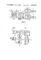
FIG. 2 illustrates circuitry to perform rotation of the color mixture signals I and Q for accomplishing tint correction. The FIG. 2 circuitry is located in the color signal processing channel of the receiver after chrominance has been extracted from composite video and the chrominance signal has been demodulated into its I and Q color mixture signal components. It will be assumed for purposes of description that the I and Q signals are in sampled data pulse code modulated (binary PCM) format. Further it will be presumed that composite video was sampled at four times the color subcarrier rate resulting in the I and Q signals samples each occurring at a two times subcarrier rate and displaced by 90 degrees. The signal sample occurrence is depicted in FIG. 3 and denoted SA and SB. The I signal samples are shown to alternate between +I and -I samples however the + and - signs are not meant to connate signal polarity but rather the phase of the sampling points relative to burst.
The recovered and demodulated color mixture signal SA (e.g. parallel 8-bit PCM samples) is applied to signal bus 10, and the recovered and demodulated color mixture signal SB is applied to signal bus 11. Signals SA and SB (i.e. Ia and Qa respectively) are applied to angle detectors 12, 13 and 14 which respectively generate control signals on output control connections 15, 16 and 17 when the tangent Ia /Qa exceeds predetermined angles, indicative of the angle of the vector sum Ca relative to Qa or Ia. Signal SA is also applied to a first input terminal 22 of a multiplexer 21, and to a one sample period delay element 20. Signal SB is applied to a second input terminal 23 of multiplexer 21 and to a second one sample period delay element 19. Signal SC (FIG. 3) from delay element 20 and signals SD from delay element 19 are respectively applied to third and fourth input terminals 24 and 25 of multiplexer 21. Multiplexer 21 clocked by signal φ2L time division multiplexes the signals SA, SB, SC and SD to form the sample sequence SE which includes alternate samples of the +I and +Q samples. The I and Q signal bandwidths are both less than one half the subcarrier frequency, but since the sample rate of each signal is twice the subcarrier rate the -I and -Q samples may be discarded without loss of information or violation of the Nyquist sampling criterion.
Signal SE is applied as multiplicand to a multiplier 31. The signals, from circuit element 29, corresponding to the sine and cosine of the angle by which the vectors are to be rotated are applied as multipliers to multiplier 31. Element 29 is a read only memory, ROM, which is clocked by signal φs/c to alternately produce the sine and cosine of angles corresponding to ROM address codes applied to ROM address input port 30. Element 29 may be a single ROM programmed to produce the sine of the address code applied when φs/c is in the logic high state, and programmed to produce the sine of 90 degrees minus the applied address code (equal to cosine of the address) when φs/c is in the logic low state. Alternatively element 29 may be a pair of parallel ROM's one of which is programmed to produce the sine of the applied address code, and the other being programmed to produce the cosine of the applied address code. Responsive to signal φs/c the pair of ROM's are alternately energized to apply multiplier signals to the multiplier 31.
Signal φs/c is timed to produce the sine of the address code for two of the signal SE sample periods and then the cosine of the same address code for two sample periods so that the sample sequence SF, available at the multiplier 31 output connection is of the form Qsinφ, Isinφ, Qcosφ, Icosφ, Qsinφ, Isinφ etc. The signal SF from multiplier 31 is applied to a latch 32 from which the signal SI is available. Latch 32 is incorporated in the signal path so that the signal samples are stable over the sample period. Signal SI from latch 32 is applied to a second latch 33 which delays the samples by one sample period. Signal from latch 33 is applied to a clocked two's complementing circuit 35 which inverts the polarity of the samples when the signal φs/c is a logic low. The sequence of samples SK from circuit 35 therefore has all sine terms inverted in polarity.
The output sequence from complementing circuit 35 and the signal sequence from latch 32 are applied to first and second input ports of ADDER 34. The one sample delay imposed on the signal SI from latch 32 by the latch 33 temporally aligns, at the adder input ports, samples which are displaced by one sample period. The consecutive pairs of samples occurring at the inputs of adder 34 are +Qcosφ,(-)Isinφ; +Icosφ,+Qcosφ; +Qsinφ, +Icosφ; +Isinφ,-Qsinφ; +Qcosφ,-Isinφ; etc. It will be recognized that the sum of the samples in every other pair will produce one of the corrected samples Ic or Qc as defined in equations (9) and (10). The sums of the samples in the intervening pairs are without meaning in the illustrated system and are therefore discarded. Adder 34 sums the signal samples SI and SK producing the signal SL. In FIG. 3 the samples SL correspond to the sum of the temporally aligned samples SI and SK immeditely above the respective SL sample. The periods designated X correspond to the meaningless sums. The signal SL is applied to latches 37 and 38 which are clocked by respective clock signals φ3L and φ3L to demultiplex the desired I and Q samples producing the demodulated signals SN and SM respectively, corresponding to rotated signals Ic and Qc.
The angle by which the vectors are rotated is determined by the address codes applied to element 29. These address codes may be manually applied (element 26) to adjust the hue of the overall scene or applied, under control of an auto flesh detector ( elements 12, 13, 14 and 18) to enhance flesh tones, or a combination of both as shown for illustrative purposes in FIG. 2. It is noted for completeness that when the chrominance angles for auto flesh enhancement are detected ahead of manual tint control, the system will not respond symmetrically for auto flesh correction since the auto flesh angles will be biased by the manual tint control angle.
Auto flesh angle detection will be described with reference to element 12 of FIG. 2, elements 13 and 14 being similar in construction. The Ia (SA) color mixture signal is applied to a first input port of subtractor element 50 and the sign bit (indicative of signal sample polarity) of the Ia signal is applied to an inverting input terminal of AND gate 53. The Qa (SB) signal is applied to element 52 which passes the absolute value |Qa | of the Qa samples. The output of element 52 is applied to a multiplier 51 which multiplies the |Qa | samples by a constant N. The multiplied |Qa | samples N|Qa | are applied to subtractor 50 which produces a signal corresponding to the polarity of the difference Ia -N|Qa | at its output terminal 54. The output terminal 54 of subtractor 50 is applied to a second input of AND gate 53 which produces a control signal on output connection 15 whenever the Ia samples are positive and the polarity of the difference is negative. (The assumption is made that the samples are in two's complement form so that the sign bit is zero for positive values and one for negative values.
When the difference Ia -N|Qa | equals zero, Ia /|Qa | equals N and the angle of the chrominance signal (vector sum of Ia and Qa) relative to the Q axis is equal to the arctangent of N. If the difference is positive or negative the chrominance angle is lesser or greater than the arctan (N) respectively. The three angle detectors 12, 13 and 14 apply three difference multiplicative constants Ni. The control signals 15, 16 and 17 from the angle detectors are therefore indicative of different chrominance angle ranges. The control signals on connections 15, 16 and 17 are applied to element 18, for example a ROM, which generates address codes on its output connection 22 that may be applied directly to ROM 29 input connection 30 or through ADDER 29 wherein the auto flesh address codes are added to the manually generated tint control codes from element 26.
Element 18 produces address codes corresponding to angles by which the vectors Ia and Qa are desired to be rotated depending upon the range of angles currently occupied by the chrominance vector. For example if the chrominance vector is between 20 and 30 degrees from the I vector the address codes may correspond to values to cause a rotation of 15 degrees. This occurs instantaneously whenever the chrominance vector enters this range.
Element 26 on the other hand produces angle address codes applicable to the chrominance vector for all angular positions of the chrominance vector. Element 26 is manually operated while the user is viewing the recovered scene to adjust the overall tint of the scene. Element 26 may be an up/down counter which when energized by the user, outputs binary address codes to rotate the chrominance vector in either direction until the scene contains a hue acceptable to the viewer. The codes from element 26 may be applied directly to ROM 29 (in the absence of auto flesh) or they may be added to the auto flesh address codes via ADDER 28.
FIG. 4 is a variant of the FIG. 2 circuit. Elements having the same designation numbers as elements in FIG. 2 are equivalents. Description of the FIG. 4 circuit will be made with reference to the sample sequences and waveforms shown in FIG. 5. In FIG. 5 the 4Fsc waveform is the sampling clock used to perform analog-to-digital conversion of composite video. The remaining waveforms φA, φB, φC, φE, φD and φF, are generated from the 4Fsc waveform using straight forward combinatorial logic as is known in the art of digital signal processing. The signal sequences SA and SB are the separated and demodulated I and Q color mixture signals as in FIG. 3. The subscripts n, n+1, n+2, etc. designate the subcarrier cycle from which the sample was digitized.
Signals SA and SB available on busses 10 and 11 are applied to multiplexer 59, which responsive to clock φA, time division multiplexes the +I and +Q signals to form the sequence of signal S'E. Signal S'E is applied to multiplier 25 wherein it is multiplied by the sine and cosine of the angle by which the vectors are to be rotated. The sines and cosines ar provided by element 29 which is energized by clock φB to produce the sequence of samples from multiplier 25 In cosφ, In sinφ, Qn sinφ, Qn cosφ, In+1 cosφ, Ik+1 sinφ etc. These values are demultiplexed into latches 51, 52, 53 and 54 by clocks φC, φD, φE and φF respectively. The Icosφ terms are successively latched in latch 51. The Qsinφ terms are latched in latch 52, the Qcosφ terms are latched in latch 53 and the Isinφ terms are latched in latch 54. The Icosφ and Qsinφ terms are applied to ADDER 56 to produce the sum Ic =Icosφ+Qsinφ. The sums are successively latched into latch 57 by clock φF to produce the sequence S'N.
The Qcosφ and Isinφ terms are applied to subtractor 55 which produces the difference Qc =Qcosφ-Isinφ. The differences are successively latched into latch 58 by clock φc to produce the sequence S'M.
FIG. 6 is a further variation which operates directly on the non-demodulated chrominance signal. Operation of the FIG. 6 circuit will be described with reference to the signal sequences and waveforms illustrated in FIG. 7. When composite video is sampled at four times subcarrier along the I and Q axis and the chrominance signal is separated from luminance, the resulting chrominance sample sequence is in the form of signal Sp in FIG. 7, i.e. -Qn-1, +In, Qn, -In, -Qn, +In+1 . . . In FIG. 6 the Sp signal is applied to multiplier 31 wherein the samples are multiplied by the sines and cosines of the angle of rotation. The sine and cosine terms are provided by ROM 29 under the control of clock φS/C which provides the sine terms during the +Q and -I samples and cosine terms during the -Q and +I samples. The sequence of terms resulting from the multiplication is the signal SQ. Signal SQ is applied to the serially connected latches 32 and 33 under control of clock 4Fsc. Delayed signal sequences from latches 32 and 33 are denoted SR and ST respectively in FIG. 7.
Signal SR is applied to complementing circuit 60 which is controlled by clock φ5L to complement the -Qcosφ and +Icosφ terms and to pass the +Qsinφ and -Isinφ terms unaltered. Signal from complementing circuit 60 and the ST signal are applied to the input ports of ADDER 34. ADDER 34 produces the sequences of sums S1 =Qo cosφ-Io sinφ; S2 -I1 cosφ-Q0 cosφ; S3 =Q1 sinφ+I1 cosφ; and S4 =-I1 sinφ+Q1 sinφ. Sums S1 correspond to samples Qc and sums S3 correspond to samples Ic according to equations (9) and (10). Sums S2 and S4 are meaningless in the system and are discarded. Sums S1 and S3 are latched by clocks φ5L and φ5L into latches 38 and 37 respectively to produce the signals SV and SW respectively.
The sequence SW of samples Ic are generated from the +I and +Q signal samples of the sequence Sp. The sequence SV of samples Qc however are generated from the -I and -Q signal samples of the sequence Sp.
Three embodiments of the invention have been described for illustrative purposes. Armed with the foregoing disclosure one skilled in the art of digital signal processing may readily generate further variations without straying from the spirit of the invention. For example the multiplication function may be performed by generating the logarithm of the multiplicand and multiplier, adding the logs and applying the sums to an antilog table. Further the sine/cosine ROM may be implemented with a programmable logic array (PLA) etc.