US4827428A - Transistor sizing system for integrated circuits - Google Patents
Transistor sizing system for integrated circuits Download PDFInfo
- Publication number
- US4827428A US4827428A US06/798,557 US79855785A US4827428A US 4827428 A US4827428 A US 4827428A US 79855785 A US79855785 A US 79855785A US 4827428 A US4827428 A US 4827428A
- Authority
- US
- United States
- Prior art keywords
- output
- circuit
- delay
- size
- integrated circuit
- Prior art date
- Legal status (The legal status is an assumption and is not a legal conclusion. Google has not performed a legal analysis and makes no representation as to the accuracy of the status listed.)
- Expired - Lifetime
Links
Images


Classifications
-
- G—PHYSICS
- G06—COMPUTING; CALCULATING OR COUNTING
- G06Q—INFORMATION AND COMMUNICATION TECHNOLOGY [ICT] SPECIALLY ADAPTED FOR ADMINISTRATIVE, COMMERCIAL, FINANCIAL, MANAGERIAL OR SUPERVISORY PURPOSES; SYSTEMS OR METHODS SPECIALLY ADAPTED FOR ADMINISTRATIVE, COMMERCIAL, FINANCIAL, MANAGERIAL OR SUPERVISORY PURPOSES, NOT OTHERWISE PROVIDED FOR
- G06Q10/00—Administration; Management
- G06Q10/04—Forecasting or optimisation specially adapted for administrative or management purposes, e.g. linear programming or "cutting stock problem"
-
- G—PHYSICS
- G06—COMPUTING; CALCULATING OR COUNTING
- G06F—ELECTRIC DIGITAL DATA PROCESSING
- G06F30/00—Computer-aided design [CAD]
- G06F30/30—Circuit design
- G06F30/32—Circuit design at the digital level
- G06F30/327—Logic synthesis; Behaviour synthesis, e.g. mapping logic, HDL to netlist, high-level language to RTL or netlist
Definitions
- This invention relates to integrated circuits and more particularly to the design and manufacture of integrated circuits that are optimized with respect to specified criteria.
- VLSI Very Large Scale Integration
- An integral part of such design tools is a means for evaluating the efficacy of the design. This includes means for measuring power consumption, speed of operation, area of the active elements, etc.
- Timing analysis is one such tool, and is an important one because it is an essential element of any transistor sizing algorithm. Of course, the timing analysis is important in its own right to the designer of the circuit.
- V. Agrawal describes an algorithm for estimating the time delay through a digital circuit. It is not the first such algorithm but it is an important one because it is able to discern the presence of latches (memory) in the circuit being investigated and is able to estimate the time delay from any input to any output of the combinatorial portion of the circuit.
- Two other timing analyzers are the Timing Verifier (TV) program by N.
- the CRYSTAL and TV programs differ from the Agrawal algorithm in that they use a more detailed timing estimation method, which takes into account differing gate delays for a single gate depending upon which input the signal arrives on.
- the drawback of both the TV and CRYSTAL programs is that they do not handle the presence of feedback in the integrated circuits, and that excludes almost all of the digital integrated circuits that are designed and built today.
- transistor sizing approach Another important aspect of integrated circuit design is the transistor sizing approach that is employed.
- transistor sizing approach There are, of course, many deterministic sizing approaches.
- One simple approach for example, is to create all transistors in one size that satisfies the circuit's overall speed requirement.
- the transistor size is related to how close the transistor is to the power (battery or ground) rail.
- Ruehli, et al. described in "Analytical Power/Timing Optimization Technique for Digital System," IEEE Proc. 14th Design Automation Conf., (June 1977), pp. 142-146.
- Timing analyzer does not have the ability to recognize and deal with the presence of memory in the circuit. It also does not take into account the additional delay accruing from increasing the size of a transistor gate and thereby increasing the capacitance that needs to be driven.
- An algorithm that does take into account the increased gate capacitance was proposed by M. Matson in "Optimization of Digital MOS VLSI Circuits," Proc. Chapel Hill Conf. on VLSI, (University of North Carolina, May 1985), pp. 109-126. Matson's algorithm also uses a more accurate delay model for the active elements, which takes into account the slope of the input waveform.
- Matson's algorithm and of all other known sizing algorithms are that they do not have the capability to automatically recognize and deal with feedback generally, and with memory elements in particular. This is a critical failing because essentially all digital integrated circuits are sequential circuits, and sequential circuits contain memory.
- Another drawback of these algorithms is their use of unnecessarily accurate optimization algorithms, which result in unacceptably show analysis of large integrated circuit designs.
- a subject design of an integrated circuit is iteratively analyzed and improved with each iteration, until a preselected constraint, such as speed of response, is met.
- the design improvement is realized by selecting a model for the delay through each active element of the circuit that is characterized by a convex function.
- a static timing analysis of the circuit is employed to identify the output that most grievously violates the specified constraint.
- an analysis of the path's timing structure identifies the active element in that path whose change in size would yield the largest improvement in performance. The size of that active element is adjusted accordingly, and the iteration is repeated.
- the interconnection pattern of subnetworks of the circuit is evaluated and rearranged to improve performance.
- FIG. 1 is a generalized description of a digital circuit which is segmented into a combinatorial logic portion and a memory portion;
- FIG. 2 illustrates the distributed RC model of an MOS transistor employed in connection with one embodiment of our invention
- FIG. 3 describes a three transistor "totem pole” interconnection, and the equivalent circuit that describes the delay through the circuit
- FIG. 4 is a flowchart providing a pictorial representation of the method employed in the system of our invention.
- FIG. 5 illustrates a two transistor circuit arrangement where the input signals to the two transistors have different times of arrival
- FIG. 6 describes the general structure of CMOS integrated circuits, with a PFET network being employed as a pull-up circuit and an NFET network being employed as a pull-down circuit;
- FIGS. 7 and 8 illustrate the need to sort elements within subnetworks of a circuit in order to optimize performance
- FIGS. 9 depicts a system embodiment of our invention.
- FIG. 10 shows the layout of a portion of an integrated circuit, realized in accordance with the principles of our invention.
- Electronic circuits can be divided into purely combinatorial circuits, and circuits that contain feedback paths.
- signals flow in one direction only and combine in different ways to achieve a desired logical state.
- circuits that contain feedback paths memory can be realized and the presence of memory makes the circuit a sequential circuit. It is well known that a sequential circuit can always be divided into a section containing purely combinational logic, and a section containing nothing but a plurality of basic memory elements e.g., flip-flops. Such a circuit subdivision is depicted in FIG. 1.
- T which is the minimum clock period at which the circuit will operate or, for unclocked paths, the propagation delay.
- A is simply the sum of transistor sizes or, stated differently, the total area of the active elements. It turns out that the area, A, is positively correlated with a number of other attributes of the circuit that should be minimized or constrained. First, as A increases the circuit requires more silicon area.
- any method of optimization is the form of the equation or function that is optimized and, more specifically, the nature or the behavior of that function.
- an optimization process that achieves its end results expeditiously is not a luxury but an absolute necessity.
- the first formulation is probably the most useful one because often the desired speed of operation (clock frequency) is given. In such a case, the first formulation can be used to fit the circuit within a system with a given clock period T. Also, unlike the other two formulations, two different circuits that are optimized separately with the same value of T are also optimal when considered jointly. This fact allows subcircuits to be optimized separately without loss of optimality in the final circuit.
- the second formulation might be used when the circuit is to be made as fast as possible, subject to constraints on silicon area, power, or yield.
- the third formulation represents a holistic approach in which both A and T are important, but have relative weights assigned to them. For example, it may be that T is important enough that one might be willing to pay for a one percent decrease in T with up to a five percent increase in A. In such a circumstance, one would set K to five.
- the second and, perhaps, the more important factor to be considered in pursuing the minimization process is the model used in representing the active elements of the circuit.
- Capacitor C g (13) is the capacitance between the gate and ground
- capacitor C d (14) is the capacitance between the drain and ground
- capacitor C s (16) is the capacitance between the source and ground.
- Switch 17 is closed when the FET is turned on
- resistor R ds (15) is the resistance between the drain and the source when the FET is on.
- the gate, source, and drain capacitances are all directly proportional to the transistor size x (channel width), while the source-to-drain resistance is inversely proportional to x.
- FIG. 3 illustrates the modeling of gate delay, in accordance with the distributed RC model of FIG. 2, for a "totem-pole" arrangement of three FETs.
- the Penfield-Rubinstein distributed RC model implies that an upper bound for the discharge time of the FIG. 3 circuit is
- R 1 , R 2 , and R 3 are equal to the R ds resistances of transistors x 1 , x 2 , and x 3 , respectively, C 1 is equal to C d of transistor x 1 plus C s of transistor x 2 , C 2 is equal to C d of transistor x 2 , plus C s of transistor x 3 , and C 3 is C d of transistor x 3 and C L .
- C 1 is below the closing switch and it speeds the gate's operation rather than slowing it down upon closure of the switch. This can clearly be seen when it is observed that the initial current flow sinks into capacitor C 1 , which appears as a short circuit, and no current flows through resistor R 1 .
- C 1 can be neglected and therefore C 1 does not appear in Equation (1).
- Equation (1) When Equation (1) is expressed as a function of transistor sizes x i , each R i is proportional to 1/x i and each C i is some constant plus terms that are each proportional to some x i .
- the constant term in C i represents the wire capacitance, and the variable term represents the capacitance of the gate, drain, or source, as the case may be.
- Equation (1) can be written as: ##EQU1## where A, B, C, and D are constants.
- Equation (3) is convex in the logarithms of the x i 's, which means that any straight line segment in N+1-dimensional space whose end points lie in the graph of the function, is itself entirely on or above the graph.
- Equation (3) belongs to a special class of convex functions called posynomials.
- the process starts with all active elements in the VLSI circuit design being set at their minimum possible size (block 100 in FIG. 4). This results in an initial design that contains the minimum active area and is the most reliable (the larger the active area, the more probable are the chip defects in manufacturing).
- circuit's description equations are arranged to conform to the FIG. 1 structure (block 100 in FIG. 4).
- an iterative process starts with a circuit analysis (from the specification resulting from the above step 2) to identify and select the output that fails most (block 110 in FIG. 4).
- a circuit analysis from the specification resulting from the above step 2 to identify and select the output that fails most (block 110 in FIG. 4).
- failed most we mean that, for example, when T is 1 microsecond, one output has a delay of 1.2 microseconds and another output has a delay of 1.5 microseconds, then the 1.5 microseconds output is selected as the output that fails most.
- the causes of the delay in the selected output are investigated by examining, in turn, each transistor which could have an effect on that output (block 120 in FIG. 4).
- two numbers are assigned to each electrical node: t 1 (latest-time-to-go-low), and t h (latest-time-to-go-high).
- t 1 latest-time-to-go-low
- t h latest-time-to-go-high
- the pull-up circuitry is examined
- t 1 causes the "failure”
- the pull-down circuitry is examined.
- Such examination includes both the active element under consideration and its supporting elements. Among the supporting elements are, of course, all the active elements that contribute to that element's input signal.
- the investigation includes all three transistors in addition to the investigation of the critical path leading to the input that happens to be the slowest.
- the iterative loop is closed (in block 140 of FIG. 4) by returning to the point of output delay determination (i.e., to block 110 in FIG. 4), until either the imposed constraint is satisfied or no transformation is possible that reduces the quantity being minimized.
- the delay curve as a function of size follows the relationship Ax+B/x+C where A, B, and C are greater than 0; which means that from some minimum value of x, as x is increased the delay is decreased until some minimum delay is reached. Beyond the size of minimum delay, continuing to increase the size increases the delay.
- a step is included in our method (block 150 in FIG. 4) that sorts the order of series subnetworks of a subcircuit within the VLSI circuit in order to improve the subnetworks' performance (speed).
- FIG. 5 depicts a series subnetwork of two transistors where the input to transistor 20 arrives with a 7 nsec delay and the input to transistor 21 arrives with a 3 nsec delay. In the timing arrangement illustrated in FIG.
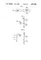
- a static CMOS complex gate consists of a pull-up network 25 and a pull-down network 26.
- the pull-up network contains only PFETS, and the pull-down network contains as many NFETS.
- the inputs to the two networks are identical, and the two networks (which are duals of each other) are connected to each other in series between V dd and ground. The connection between the two networks forms the output of the gate.
- a network with two connection points and any number of inputs can be constructed from single transistors by any recursive composition of the following three rules:
- a single transistor is a network.
- the source and drain are the two connection points, and the gate is the single input of the network.
- Any number of networks can have their connection points connected in series to form another network (e.g., FIG. 5).
- the new network's inputs are the union of the inputs of the component networks.
- the new network's connection points are the two connection points of the components left free.
- Any number of networks can have their connection points connected in parallel to form another network.
- the new network's inputs are the union of the inputs of the component networks.
- the new network's connection points are the connection points of the component networks that have been connected.
- this latest-time-to-turn-on is the maximum of the latest-time-to-turn-on values of the constituent transistors.
- the latest-time-to-turn-on of an NFET is the latest-fime-to-go-high of its gate.
- the latest-time-to-turn-on of a PFET is the latest-time-to-go-low of its gate.
- FIGS. 7 and 8 illustrate this process with a complex gate that contains 14 transistors.
- FIG. 7 is before sorting and FIG. 8 is after sorting.
- the latest-time-to-go-high and the latest-time-to-go-low of inputs A, B, C, and D are ordered A 1 ⁇ B 1 ⁇ C 1 ⁇ D 1 and A h ⁇ C h ⁇ B h ⁇ D h .
- the three transistors in series are already in optimal order: A should be closest to V dd , since its latest-time-to-go-low is earliest, followed by B and then C.
- the pull-up is composed of subnetworks 30 and 31 in series, and these networks are in their own order; subnetwork 31, which has a latest-time-to-turn-on that is earlier than that of subnetwork 30, should be closest to V dd . Accordingly, in FIG. 8, the positions of subnetworks 30 and 31 are reversed. Meanwhile, in the pull-down subnetwork, 32, one reordering needs to be made; and that is in the three transistors in series. Transistor B should be closest to the output followed by C, followed by A. This rearrangement within subnetwork 32 is also shown in FIG. 8.
- Block 151 is a timing analyzer which receives as input the specification of the circuit whose layout is to be optimized. It contains a model representing the active elements of the circuit which yields a convex delay function. With the aid of that model and under control of block 157, block 151 analyzes the specification (as taught, for example, by V. Agrawal) and develops a table that correlates the outputs of the circuit with approximated time delays. That table is stored in memory 156. Control then passes to block 152 which obtains the speed criteria to be satisified from control block 157 and selects that output from the table created by block 151 which fails the speed criteria by the greatest amount.
- Each active element in the identified critical path is evaluated to determine its sensitivity to changes in size by evaluating the incremental change in delay for a given incremental change in size (from the existing size). It may be noted here that all active elements begin with some initial minimum size. The active element that is found to have the greatest incremental improvement in delay is selected, and its changed size specification is noted in another table within memory 156.
- Control then passes to block 155, where the effect on output delays caused by the change in size effected by block 155 is evaluated. The results of this evaluation are fed to block 157, where the resultant collection of circuit output delays and active element sizes (from the tables in memory 156) is compared to the operational criteria provided to block 157.
- Control is returned to block 152 until the criteria are met.
- the operational criteria considered can be minimizing the integrated circuit area subject to the requirement that a certain speed is achieved, minimizing the delay through the circuit subject to the requirement that integrated circuit's area should not exceed a certain value; or a combination of the above.
- Other criteria can, of course, be also accommodated.
- the step of selecting the minimum size of transistors is taken simply on the advice of the integrated circuit manufacturer.
- the step of separating a circuit's specification into a combinatorial portion and a memory is well known and, indeed, the aforementioned Agrawal timing analyzer incorporates this step and therefore can be used in the implementation of our system and method.
- the outputs of the combinatorial portion that go solely to the memory are, nevertheless, treated as outputs, the delays of which are considered as described above.
- the output of the timing analyzer is a table that correlates the circuits' outputs to the delay of those outputs. From this table, the worst output is selected and the "walk" backwards begins. Based on the specification of the subnetwork developing the worst output, with the aid of the distributed RC model, the effect of each transistor in that subnetwork is computed. Also, the input to the subnetwork that constitutes the critical input as far as delay is concerned is identified. The transistor in the subnetwork that is found to yield the largest improvement in performance is remembered and the process continues with the analysis of the subnetwork that feeds the critical input. With each subnetwork analysis, a transistor offering the largest improvement in performance is compared with the remembered transistor, and the one offering the larger improvement in performance is kept.
- the transistor remembered is the one within the entire critical path that offers the largest improvement in performance.
- the size of that transistor is altered and an updated timing analysis of that output is performed and placed in the table. The process is then reiterated with a new worst output selected and analyzed.
- Each logic subnetwork has a limited number of inputs which generally is relatively small (e.g., ⁇ 10) and the number of possible permutations is therefore manageable.
- Each subnetwork in the critical path is evaluated and a sorting of the inputs is suggested based on the latest-time-to-turn-on of each subnetwork.
- a simple "bubble-sort" algorithm is employed to effect the actual subnetwork sorting.
- FIG. 10 illustrates a sample layout that results from application of our invention. Shown are MOS transistors with different sizes (channel widths) that were determined to yield, in combination, the maximum speed in a given area.
Abstract
Description
(R.sub.1 +R.sub.2)C.sub.2 +(R.sub.1 +R.sub.2 +R.sub.3)C.sub.3, (1)
Claims (20)
Priority Applications (8)
| Application Number | Priority Date | Filing Date | Title |
|---|---|---|---|
| US06/798,557 US4827428A (en) | 1985-11-15 | 1985-11-15 | Transistor sizing system for integrated circuits |
| EP86308706A EP0223526B1 (en) | 1985-11-15 | 1986-11-07 | Integrated circuit and optimization method therefore |
| DE3689538T DE3689538T2 (en) | 1985-11-15 | 1986-11-07 | Integrated circuit and optimization process for it. |
| JP61-269991A JP3004650B2 (en) | 1985-11-15 | 1986-11-14 | Optimized integrated circuit |
| CA000522987A CA1258911A (en) | 1985-11-15 | 1986-11-14 | Optimized integrated circuits |
| KR1019860009619A KR960002546B1 (en) | 1985-11-15 | 1986-11-14 | Transistor sizing system for integrated circuit |
| SG44094A SG44094G (en) | 1985-11-15 | 1994-03-25 | Integrated circuit and optimization method therefore |
| HK104694A HK104694A (en) | 1985-11-15 | 1994-09-29 | Integrated circuit and optimization method therefore |
Applications Claiming Priority (2)
| Application Number | Priority Date | Filing Date | Title |
|---|---|---|---|
| US06/798,557 US4827428A (en) | 1985-11-15 | 1985-11-15 | Transistor sizing system for integrated circuits |
| SG44094A SG44094G (en) | 1985-11-15 | 1994-03-25 | Integrated circuit and optimization method therefore |
Publications (1)
| Publication Number | Publication Date |
|---|---|
| US4827428A true US4827428A (en) | 1989-05-02 |
Family
ID=26663988
Family Applications (1)
| Application Number | Title | Priority Date | Filing Date |
|---|---|---|---|
| US06/798,557 Expired - Lifetime US4827428A (en) | 1985-11-15 | 1985-11-15 | Transistor sizing system for integrated circuits |
Country Status (6)
| Country | Link |
|---|---|
| US (1) | US4827428A (en) |
| EP (1) | EP0223526B1 (en) |
| CA (1) | CA1258911A (en) |
| DE (1) | DE3689538T2 (en) |
| HK (1) | HK104694A (en) |
| SG (1) | SG44094G (en) |
Cited By (103)
| Publication number | Priority date | Publication date | Assignee | Title |
|---|---|---|---|---|
| WO1990011569A1 (en) * | 1989-03-24 | 1990-10-04 | Vantage Analysis Systems, Inc. | Computer-aided engineering |
| US5003487A (en) * | 1988-06-28 | 1991-03-26 | International Business Machines Corporation | Method and apparatus for performing timing correction transformations on a technology-independent logic model during logic synthesis |
| GB2244829A (en) * | 1989-01-13 | 1991-12-11 | Vlsi Technology Inc | Method for analyzing datapath elements |
| US5133063A (en) * | 1987-07-29 | 1992-07-21 | Hitachi, Ltd. | Method and system for outputting program change effect information to a user |
| US5157668A (en) * | 1989-07-05 | 1992-10-20 | Applied Diagnostics, Inc. | Method and apparatus for locating faults in electronic units |
| US5175843A (en) * | 1989-10-30 | 1992-12-29 | General Electric Company | Computer-aided design method for restructuring computational networks to minimize shimming delays |
| US5218551A (en) * | 1990-04-30 | 1993-06-08 | International Business Machines Corporation | Timing driven placement |
| WO1993024895A2 (en) * | 1992-06-04 | 1993-12-09 | Xilinx, Inc. | Timing driven method for laying out a user's circuit onto a programmable integrated circuit device |
| US5305229A (en) * | 1991-09-06 | 1994-04-19 | Bell Communications Research, Inc. | Switch-level timing simulation based on two-connected components |
| US5359534A (en) * | 1991-01-22 | 1994-10-25 | Rohm Co., Ltd. | Verification method of logical circuit layout patterns |
| US5392221A (en) * | 1991-06-12 | 1995-02-21 | International Business Machines Corporation | Procedure to minimize total power of a logic network subject to timing constraints |
| US5404310A (en) * | 1989-10-17 | 1995-04-04 | Kabushiki Kaisha Toshiba | Method and apparatus for power-source wiring design of semiconductor integrated circuits |
| US5404311A (en) * | 1991-10-17 | 1995-04-04 | Fujitsu Limited | Method of optimizing delay times |
| WO1995010094A2 (en) * | 1993-10-06 | 1995-04-13 | Nsoft Systems, Inc. | Process independent design for gate array devices |
| GB2283117A (en) * | 1993-08-13 | 1995-04-26 | Harris Corp | Interactively tailoring topography of integrated circuit layout in accordance with electromigration model-based minimum width metal and contact/via rules |
| US5422317A (en) * | 1993-01-28 | 1995-06-06 | Advanced Micro Devices, Inc. | Performance enhanced intergrated circuit layout methodology |
| US5436849A (en) * | 1993-02-09 | 1995-07-25 | International Business Machines Corporation | Incremental logic synthesis system for efficient revision of logic circuit designs |
| US5459673A (en) * | 1990-10-29 | 1995-10-17 | Ross Technology, Inc. | Method and apparatus for optimizing electronic circuits |
| US5461575A (en) * | 1991-04-26 | 1995-10-24 | Motorola, Inc. | Simulation of sequential circuits for calculating timing characteristics to design/manufacture a logic network |
| US5477467A (en) * | 1989-07-17 | 1995-12-19 | Motorola, Inc. | Shrinkable BiCMOS circuit layout |
| US5481469A (en) * | 1993-09-13 | 1996-01-02 | Vlsi Technology, Inc. | Automatic power vector generation for sequential circuits |
| US5500805A (en) * | 1993-10-06 | 1996-03-19 | Nsoft Systems, Inc. | Multiple source equalization design utilizing metal interconnects for gate arrays and embedded arrays |
| US5508937A (en) * | 1993-04-16 | 1996-04-16 | International Business Machines Corporation | Incremental timing analysis |
| US5510999A (en) * | 1993-10-06 | 1996-04-23 | Nsoft Systems, Inc. | Multiple source equalization design for gate arrays and embedded arrays |
| US5515302A (en) * | 1994-11-07 | 1996-05-07 | Motorola, Inc. | Method for identifying excessive power consumption sites within a circuit |
| US5517649A (en) * | 1994-04-19 | 1996-05-14 | Maxtor Corporation | Adaptive power management for hard disk drives |
| US5548526A (en) * | 1992-03-11 | 1996-08-20 | Vlsi Technology, Inc. | Timing model and characterization system for logic simulation of integrated circuits |
| US5596505A (en) * | 1993-07-23 | 1997-01-21 | Vlsi Technology, Inc. | Estimation of pin-to-pin timing for compiled blocks |
| US5602754A (en) * | 1994-11-30 | 1997-02-11 | International Business Machines Corporation | Parallel execution of a complex task partitioned into a plurality of entities |
| US5612636A (en) * | 1995-01-19 | 1997-03-18 | Texas Instruments Incorporated | Short circuit power optimization for CMOS circuits |
| US5619420A (en) * | 1995-05-04 | 1997-04-08 | Lsi Logic Corporation | Semiconductor cell having a variable transistor width |
| US5633807A (en) * | 1995-05-01 | 1997-05-27 | Lucent Technologies Inc. | System and method for generating mask layouts |
| US5636372A (en) * | 1994-09-30 | 1997-06-03 | International Business Machines Corporation | Network timing analysis method which eliminates timing variations between signals traversing a common circuit path |
| US5640328A (en) * | 1994-04-25 | 1997-06-17 | Lam; Jimmy Kwok-Ching | Method for electric leaf cell circuit placement and timing determination |
| US5654898A (en) * | 1993-05-10 | 1997-08-05 | Cascade Design Automation Corporation | Timing-driven integrated circuit layout through device sizing |
| US5663889A (en) * | 1993-12-28 | 1997-09-02 | Fujitsu Limited | Apparatus for computing delay time of integrated circuit |
| US5663888A (en) * | 1993-03-30 | 1997-09-02 | Nec Usa, Inc. | Redesign of sequential circuits to reduce clock period |
| US5684723A (en) * | 1987-11-16 | 1997-11-04 | Fujitsu Limited | Device simulation method and device simulator |
| US5687088A (en) * | 1993-05-19 | 1997-11-11 | Matsushita Electric Industrial Co., Ltd. | Net list for use in logic simulation and back annotation method of feedbacking delay information obtained through layout design to logic simulation |
| USRE35671E (en) * | 1990-12-13 | 1997-11-25 | Vlsi Technology, Inc. | Predictive capacitance layout method for integrated circuits |
| US5703798A (en) * | 1995-04-25 | 1997-12-30 | Mentor Graphics Corporation | Switch level simulation employing dynamic short-circuit ratio |
| US5724250A (en) * | 1996-02-07 | 1998-03-03 | Unisys Corporation | Method and apparatus for performing drive strength adjust optimization in a circuit design |
| US5737580A (en) * | 1995-04-28 | 1998-04-07 | International Business Machines Corporation | Wiring design tool improvement for avoiding electromigration by determining optimal wire widths |
| US5751593A (en) * | 1996-04-10 | 1998-05-12 | Motorola, Inc. | Accurate delay prediction based on multi-model analysis |
| US5764531A (en) * | 1995-03-14 | 1998-06-09 | Kabushiki Kaisha Toshiba | Sizing apparatus for active devices of integrated circuits and sizing method therefor |
| US5787008A (en) * | 1996-04-10 | 1998-07-28 | Motorola, Inc. | Simulation corrected sensitivity |
| US5790415A (en) * | 1996-04-10 | 1998-08-04 | Pullela; Satyamurthy | Complementary network reduction for load modeling |
| US5841672A (en) * | 1996-02-13 | 1998-11-24 | Vlsi Technology, Inc. | Method and apparatus for verifying signal timing of electrical circuits |
| US5841674A (en) * | 1995-12-14 | 1998-11-24 | Viewlogic Systems, Inc. | Circuit design methods and tools |
| US5880967A (en) * | 1995-05-01 | 1999-03-09 | Synopsys, Inc. | Minimization of circuit delay and power through transistor sizing |
| US5903471A (en) * | 1997-03-03 | 1999-05-11 | Motorola, Inc. | Method for optimizing element sizes in a semiconductor device |
| US5946475A (en) * | 1997-01-21 | 1999-08-31 | International Business Machines Corporation | Method for performing transistor-level static timing analysis of a logic circuit |
| US5974244A (en) * | 1996-06-13 | 1999-10-26 | Kabushiki Kaisha Toshiba | Layout pattern generation device for semiconductor integrated circuits and method therefor |
| US6014510A (en) * | 1996-11-27 | 2000-01-11 | International Business Machines Corporation | Method for performing timing analysis of a clock circuit |
| US6023567A (en) * | 1996-10-07 | 2000-02-08 | International Business Machines Corporation | Method and apparatus for verifying timing rules for an integrated circuit design |
| US6074429A (en) * | 1997-03-03 | 2000-06-13 | Motorola, Inc. | Optimizing combinational circuit layout through iterative restructuring |
| US6128769A (en) * | 1997-12-31 | 2000-10-03 | Intel Corporation | Method for analyzing and efficiently reducing signal cross-talk noise |
| US6148434A (en) * | 1996-09-18 | 2000-11-14 | Kabushiki Kaisha Toshiba | Apparatus and method for minimizing the delay times in a semiconductor device |
| US6175949B1 (en) * | 1998-03-24 | 2001-01-16 | International Business Machines Corporation | Method and system for selecting sizes of components for integrated circuits |
| US6185723B1 (en) | 1996-11-27 | 2001-02-06 | International Business Machines Corporation | Method for performing timing analysis of a clock-shaping circuit |
| US6269277B1 (en) * | 1998-07-27 | 2001-07-31 | The Leland Stanford Junior University Board Of Trustees | System and method for designing integrated circuits |
| US6269468B1 (en) | 1999-03-02 | 2001-07-31 | International Business Machines Corporation | Split I/O circuit for performance optimization of digital circuits |
| US6272668B1 (en) | 1994-12-14 | 2001-08-07 | Hyundai Electronics America, Inc. | Method for cell swapping to improve pre-layout to post-layout timing |
| US6289490B1 (en) | 1997-10-31 | 2001-09-11 | The Board Of Trustees Of The Leland Stanford Junior University | Optimization of integrated circuit properties through constraints using a dominant time constant |
| US6311145B1 (en) * | 1999-06-17 | 2001-10-30 | The Board Of Trustees Of The Leland Stanford Junior University | Optimal design of an inductor and inductor circuit |
| US6393601B1 (en) | 1997-04-14 | 2002-05-21 | Matsushita Electric Industrial Co., Ltd. | Layout designing apparatus for integrated circuit, transistor size determining apparatus, circuit characteristic evaluating method, and transistor size determining method |
| US20020157079A1 (en) * | 2001-04-24 | 2002-10-24 | International Business Machines Corporation | CMOS tapered gate and synthesis method |
| US20020184603A1 (en) * | 2001-04-25 | 2002-12-05 | Arash Hassibi | Optimal simultaneous design and floorplanning of integrated circuit |
| WO2002101599A1 (en) * | 2001-06-12 | 2002-12-19 | Conexant Systems, Inc. | Method and system for predictive mosfet layout generation with reduced design cycle |
| US20030061784A1 (en) * | 2001-10-01 | 2003-04-03 | Van Der Drift Gerardus Petrus Maria | Glasshouse construction |
| US6629301B1 (en) | 2000-09-15 | 2003-09-30 | Sun Microsystems, Inc. | Determining transistor widths using the theory of logical effort |
| US20030191611A1 (en) * | 2002-04-05 | 2003-10-09 | Hershenson Maria Del Mar | Behavioral circuit modeling for geometric programming |
| US6640331B2 (en) * | 2001-11-29 | 2003-10-28 | Sun Microsystems, Inc. | Decoupling capacitor assignment technique with respect to leakage power |
| US20040015787A1 (en) * | 2002-04-10 | 2004-01-22 | Thomas Heydler | Method and apparatus for efficient semiconductor process evaluation |
| US20040027206A1 (en) * | 2002-04-07 | 2004-02-12 | Dave Colleran | Automatic phase lock loop design using geometric programming |
| US20040172609A1 (en) * | 2002-03-05 | 2004-09-02 | Arash Hassibi | Method and apparatus for automatic analog/mixed signal system design using geometric programming |
| US20040230924A1 (en) * | 2003-05-12 | 2004-11-18 | International Business Machines Corporation | Method for tuning a digital design for synthesized random logic circuit macros in a continuous design space with optional insertion of multiple threshold voltage devices |
| US20050064347A1 (en) * | 2003-09-24 | 2005-03-24 | Yao-Ting Wang | Frequency division multiplexing (FDM) lithography |
| US20050108666A1 (en) * | 2003-11-06 | 2005-05-19 | Li-Fu Chang | Delta information design closure in integrated circuit fabrication |
| US20050172244A1 (en) * | 2002-05-15 | 2005-08-04 | Meyer Michael J. | Method and apparatus for optimizing distributed multiplexed bus interconnects |
| US20050172251A1 (en) * | 2003-11-06 | 2005-08-04 | Li-Fu Chang | Delta-geometry timing prediction in integrated circuit fabrication |
| US20050273732A1 (en) * | 2004-06-04 | 2005-12-08 | Yang Xu | Optimization and design method for configurable analog circuits and devices |
| US20050278659A1 (en) * | 2004-05-27 | 2005-12-15 | Xiaonan Zhang | Cell library providing transistor size information for automatic circuit design |
| US20050278658A1 (en) * | 2004-05-27 | 2005-12-15 | Xiaonan Zhang | Standard cell library having cell drive strengths selected according to delay |
| US20050278660A1 (en) * | 2004-05-27 | 2005-12-15 | Xiaonan Zhang | Automatic circuit design method with a cell library providing transistor size information |
| US20060107239A1 (en) * | 2004-05-27 | 2006-05-18 | Verisilicon Holdings, Co., Ltd. | Standard cell library having cell drive strengths selected according to delay |
| US20060193329A1 (en) * | 2005-02-28 | 2006-08-31 | Rajiv Asati | Method and apparatus for limiting VPNv4 prefixes per VPN in an inter-autonomous system environment |
| US20060236279A1 (en) * | 2005-03-24 | 2006-10-19 | Fujitsu Limited | Design supporting apparatus, design supporting method, and computer product |
| US20060242618A1 (en) * | 2005-02-14 | 2006-10-26 | Yao-Ting Wang | Lithographic simulations using graphical processing units |
| US20070094623A1 (en) * | 2005-10-24 | 2007-04-26 | Haizhou Chen | Timing, noise, and power analysis of integrated circuits |
| US20070113211A1 (en) * | 2005-11-17 | 2007-05-17 | Lizheng Zhang | Efficient statistical timing analysis of circuits |
| US7299459B1 (en) | 2000-01-19 | 2007-11-20 | Sabio Labs, Inc. | Parser for signomial and geometric programs |
| US20080072183A1 (en) * | 2004-09-30 | 2008-03-20 | Mar Hershenson | Novel optimization for circuit design |
| US20080320428A1 (en) * | 2007-06-22 | 2008-12-25 | Synopsys, Inc. | Minimizing Effects of Interconnect Variations in Integrated Circuit Designs |
| CN100565677C (en) * | 2003-12-05 | 2009-12-02 | 阿尔法艾斯股份公司 | Measuring device for optically measuring properties of a measurement object |
| US20100042564A1 (en) * | 2008-08-15 | 2010-02-18 | Beverly Harrison | Techniques for automatically distingusihing between users of a handheld device |
| US7735048B1 (en) * | 2003-11-24 | 2010-06-08 | Cadence Design Systems, Inc. | Achieving fast parasitic closure in a radio frequency integrated circuit synthesis flow |
| US8245167B1 (en) * | 2008-02-14 | 2012-08-14 | Cadence Design Systems, Inc. | Branch and bound techniques for computation of critical timing conditions |
| US20130006898A1 (en) * | 2011-07-01 | 2013-01-03 | Phielipp Mariano J | System, method and computer program product for identity inference in a user device |
| US8527935B1 (en) | 2013-01-07 | 2013-09-03 | Freescale Semiconductor, Inc | System for reducing power consumption of electronic circuit |
| US8762922B1 (en) | 2013-10-13 | 2014-06-24 | Freescale Semiconductor, Inc. | System for reducing leakage power of electronic circuit |
| US9230050B1 (en) | 2014-09-11 | 2016-01-05 | The United States Of America, As Represented By The Secretary Of The Air Force | System and method for identifying electrical properties of integrate circuits |
| US10216890B2 (en) | 2004-04-21 | 2019-02-26 | Iym Technologies Llc | Integrated circuits having in-situ constraints |
Families Citing this family (1)
| Publication number | Priority date | Publication date | Assignee | Title |
|---|---|---|---|---|
| US5121003A (en) * | 1990-10-10 | 1992-06-09 | Hal Computer Systems, Inc. | Zero overhead self-timed iterative logic |
Citations (4)
| Publication number | Priority date | Publication date | Assignee | Title |
|---|---|---|---|---|
| US4198697A (en) * | 1978-06-15 | 1980-04-15 | Texas Instruments Incorporated | Multiple dummy cell layout for MOS random access memory |
| US4495628A (en) * | 1982-06-17 | 1985-01-22 | Storage Technology Partners | CMOS LSI and VLSI chips having internal delay testing capability |
| US4587480A (en) * | 1982-06-17 | 1986-05-06 | Storage Technology Partners | Delay testing method for CMOS LSI and VLSI integrated circuits |
| US4698760A (en) * | 1985-06-06 | 1987-10-06 | International Business Machines | Method of optimizing signal timing delays and power consumption in LSI circuits |
-
1985
- 1985-11-15 US US06/798,557 patent/US4827428A/en not_active Expired - Lifetime
-
1986
- 1986-11-07 DE DE3689538T patent/DE3689538T2/en not_active Expired - Lifetime
- 1986-11-07 EP EP86308706A patent/EP0223526B1/en not_active Expired - Lifetime
- 1986-11-14 CA CA000522987A patent/CA1258911A/en not_active Expired
-
1994
- 1994-03-25 SG SG44094A patent/SG44094G/en unknown
- 1994-09-29 HK HK104694A patent/HK104694A/en not_active IP Right Cessation
Patent Citations (4)
| Publication number | Priority date | Publication date | Assignee | Title |
|---|---|---|---|---|
| US4198697A (en) * | 1978-06-15 | 1980-04-15 | Texas Instruments Incorporated | Multiple dummy cell layout for MOS random access memory |
| US4495628A (en) * | 1982-06-17 | 1985-01-22 | Storage Technology Partners | CMOS LSI and VLSI chips having internal delay testing capability |
| US4587480A (en) * | 1982-06-17 | 1986-05-06 | Storage Technology Partners | Delay testing method for CMOS LSI and VLSI integrated circuits |
| US4698760A (en) * | 1985-06-06 | 1987-10-06 | International Business Machines | Method of optimizing signal timing delays and power consumption in LSI circuits |
Non-Patent Citations (18)
| Title |
|---|
| "An Electrical Optimizer that Considers Physical Layout" by F. W. Obermeier et al., 25th ACM/IEEE Design Automation Conference, 1988, pp. 453-459. |
| "Analytical Power/Timing Optimization Technique for Digital System," IEEE Proc. 14th Design Automation Conf., A. E. Ruehli, Jun. 1977, pp. 142-146. |
| "Electrical Optimization of PLAs," IEEE 22nd Design Automation Conf., K. S. Hedlund, 1985, pp. 681-687. |
| "Optimization of Digital MOS VLSI Circuits," Proc. Chapel Hill Conf. on VLSI, M. D. Matson, University of North Carolina, May 1985, pp. 109-126. |
| "Signal Delay in General RC Networks with Application to Timing Simulation of Digital Integrated Circuits," 1984 Conf. on Advanced Research in VLSI, T. Lin et al., MIT Jan. 1984, pp. 93-99. |
| "Signal Delay in RC Tree Networks," IEEE Transactions on Computer Aided Design, J. Rubinstein, Jul. 1983, vol. CAD-2, No. 3, pp. 202-210. |
| "Switch-Level Delay Models for Digital MOS VLSI," IEEE 21st Design Automation Conf., J. K. Ousterhout, 1984, pp. 542-548. |
| "Synchronous Path Analysis in MOS Circuit Simulator," IEEE Proc. 19th Design Automation Conf., V. D. Agrawal, 1982, pp. 629-635. |
| "Timing Analysis for nMOS VLSI," IEEE 20th Design Automation Conf., N. P. Jouppi, 1983, pp. 411-418. |
| An Electrical Optimizer that Considers Physical Layout by F. W. Obermeier et al., 25th ACM/IEEE Design Automation Conference, 1988, pp. 453 459. * |
| Analytical Power/Timing Optimization Technique for Digital System, IEEE Proc. 14th Design Automation Conf., A. E. Ruehli, Jun. 1977, pp. 142 146. * |
| Electrical Optimization of PLAs, IEEE 22nd Design Automation Conf., K. S. Hedlund, 1985, pp. 681 687. * |
| Optimization of Digital MOS VLSI Circuits, Proc. Chapel Hill Conf. on VLSI, M. D. Matson, University of North Carolina, May 1985, pp. 109 126. * |
| Signal Delay in General RC Networks with Application to Timing Simulation of Digital Integrated Circuits, 1984 Conf. on Advanced Research in VLSI, T. Lin et al., MIT Jan. 1984, pp. 93 99. * |
| Signal Delay in RC Tree Networks, IEEE Transactions on Computer Aided Design, J. Rubinstein, Jul. 1983, vol. CAD 2, No. 3, pp. 202 210. * |
| Switch Level Delay Models for Digital MOS VLSI, IEEE 21st Design Automation Conf., J. K. Ousterhout, 1984, pp. 542 548. * |
| Synchronous Path Analysis in MOS Circuit Simulator, IEEE Proc. 19th Design Automation Conf., V. D. Agrawal, 1982, pp. 629 635. * |
| Timing Analysis for nMOS VLSI, IEEE 20th Design Automation Conf., N. P. Jouppi, 1983, pp. 411 418. * |
Cited By (153)
| Publication number | Priority date | Publication date | Assignee | Title |
|---|---|---|---|---|
| US5133063A (en) * | 1987-07-29 | 1992-07-21 | Hitachi, Ltd. | Method and system for outputting program change effect information to a user |
| US5684723A (en) * | 1987-11-16 | 1997-11-04 | Fujitsu Limited | Device simulation method and device simulator |
| US5003487A (en) * | 1988-06-28 | 1991-03-26 | International Business Machines Corporation | Method and apparatus for performing timing correction transformations on a technology-independent logic model during logic synthesis |
| GB2244829B (en) * | 1989-01-13 | 1993-01-13 | Vlsi Technology Inc | Method for analyzing datapath elements |
| GB2244829A (en) * | 1989-01-13 | 1991-12-11 | Vlsi Technology Inc | Method for analyzing datapath elements |
| US5111413A (en) * | 1989-03-24 | 1992-05-05 | Vantage Analysis Systems, Inc. | Computer-aided engineering |
| WO1990011569A1 (en) * | 1989-03-24 | 1990-10-04 | Vantage Analysis Systems, Inc. | Computer-aided engineering |
| US5157668A (en) * | 1989-07-05 | 1992-10-20 | Applied Diagnostics, Inc. | Method and apparatus for locating faults in electronic units |
| US5477467A (en) * | 1989-07-17 | 1995-12-19 | Motorola, Inc. | Shrinkable BiCMOS circuit layout |
| US5404310A (en) * | 1989-10-17 | 1995-04-04 | Kabushiki Kaisha Toshiba | Method and apparatus for power-source wiring design of semiconductor integrated circuits |
| US5175843A (en) * | 1989-10-30 | 1992-12-29 | General Electric Company | Computer-aided design method for restructuring computational networks to minimize shimming delays |
| US5218551A (en) * | 1990-04-30 | 1993-06-08 | International Business Machines Corporation | Timing driven placement |
| US5459673A (en) * | 1990-10-29 | 1995-10-17 | Ross Technology, Inc. | Method and apparatus for optimizing electronic circuits |
| USRE35671E (en) * | 1990-12-13 | 1997-11-25 | Vlsi Technology, Inc. | Predictive capacitance layout method for integrated circuits |
| US5359534A (en) * | 1991-01-22 | 1994-10-25 | Rohm Co., Ltd. | Verification method of logical circuit layout patterns |
| US5461575A (en) * | 1991-04-26 | 1995-10-24 | Motorola, Inc. | Simulation of sequential circuits for calculating timing characteristics to design/manufacture a logic network |
| US5392221A (en) * | 1991-06-12 | 1995-02-21 | International Business Machines Corporation | Procedure to minimize total power of a logic network subject to timing constraints |
| US5305229A (en) * | 1991-09-06 | 1994-04-19 | Bell Communications Research, Inc. | Switch-level timing simulation based on two-connected components |
| US5404311A (en) * | 1991-10-17 | 1995-04-04 | Fujitsu Limited | Method of optimizing delay times |
| US5548526A (en) * | 1992-03-11 | 1996-08-20 | Vlsi Technology, Inc. | Timing model and characterization system for logic simulation of integrated circuits |
| WO1993024895A3 (en) * | 1992-06-04 | 1994-02-17 | Xilinx Inc | Timing driven method for laying out a user's circuit onto a programmable integrated circuit device |
| WO1993024895A2 (en) * | 1992-06-04 | 1993-12-09 | Xilinx, Inc. | Timing driven method for laying out a user's circuit onto a programmable integrated circuit device |
| US5422317A (en) * | 1993-01-28 | 1995-06-06 | Advanced Micro Devices, Inc. | Performance enhanced intergrated circuit layout methodology |
| US5436849A (en) * | 1993-02-09 | 1995-07-25 | International Business Machines Corporation | Incremental logic synthesis system for efficient revision of logic circuit designs |
| US5663888A (en) * | 1993-03-30 | 1997-09-02 | Nec Usa, Inc. | Redesign of sequential circuits to reduce clock period |
| US5508937A (en) * | 1993-04-16 | 1996-04-16 | International Business Machines Corporation | Incremental timing analysis |
| US5654898A (en) * | 1993-05-10 | 1997-08-05 | Cascade Design Automation Corporation | Timing-driven integrated circuit layout through device sizing |
| US5687088A (en) * | 1993-05-19 | 1997-11-11 | Matsushita Electric Industrial Co., Ltd. | Net list for use in logic simulation and back annotation method of feedbacking delay information obtained through layout design to logic simulation |
| US5596505A (en) * | 1993-07-23 | 1997-01-21 | Vlsi Technology, Inc. | Estimation of pin-to-pin timing for compiled blocks |
| US5581475A (en) * | 1993-08-13 | 1996-12-03 | Harris Corporation | Method for interactively tailoring topography of integrated circuit layout in accordance with electromigration model-based minimum width metal and contact/via rules |
| GB2283117A (en) * | 1993-08-13 | 1995-04-26 | Harris Corp | Interactively tailoring topography of integrated circuit layout in accordance with electromigration model-based minimum width metal and contact/via rules |
| GB2283117B (en) * | 1993-08-13 | 1998-04-29 | Harris Corp | Method for interactively tailoring the topography of an integrated circuit layout in accordance with electromigration model-based ... rules |
| US5481469A (en) * | 1993-09-13 | 1996-01-02 | Vlsi Technology, Inc. | Automatic power vector generation for sequential circuits |
| WO1995010094A2 (en) * | 1993-10-06 | 1995-04-13 | Nsoft Systems, Inc. | Process independent design for gate array devices |
| WO1995010094A3 (en) * | 1993-10-06 | 1995-04-27 | Nsoft Systems Inc | Process independent design for gate array devices |
| US5500805A (en) * | 1993-10-06 | 1996-03-19 | Nsoft Systems, Inc. | Multiple source equalization design utilizing metal interconnects for gate arrays and embedded arrays |
| US5510999A (en) * | 1993-10-06 | 1996-04-23 | Nsoft Systems, Inc. | Multiple source equalization design for gate arrays and embedded arrays |
| US5563801A (en) * | 1993-10-06 | 1996-10-08 | Nsoft Systems, Inc. | Process independent design for gate array devices |
| US5663889A (en) * | 1993-12-28 | 1997-09-02 | Fujitsu Limited | Apparatus for computing delay time of integrated circuit |
| US5517649A (en) * | 1994-04-19 | 1996-05-14 | Maxtor Corporation | Adaptive power management for hard disk drives |
| US5640328A (en) * | 1994-04-25 | 1997-06-17 | Lam; Jimmy Kwok-Ching | Method for electric leaf cell circuit placement and timing determination |
| US5636372A (en) * | 1994-09-30 | 1997-06-03 | International Business Machines Corporation | Network timing analysis method which eliminates timing variations between signals traversing a common circuit path |
| US5515302A (en) * | 1994-11-07 | 1996-05-07 | Motorola, Inc. | Method for identifying excessive power consumption sites within a circuit |
| US5615127A (en) * | 1994-11-30 | 1997-03-25 | International Business Machines Corporation | Parallel execution of a complex task partitioned into a plurality of entities |
| US5748489A (en) * | 1994-11-30 | 1998-05-05 | International Business Machines Corporation | Parallel execution of a complex task partitioned into a plurality of entities |
| US5602754A (en) * | 1994-11-30 | 1997-02-11 | International Business Machines Corporation | Parallel execution of a complex task partitioned into a plurality of entities |
| US6272668B1 (en) | 1994-12-14 | 2001-08-07 | Hyundai Electronics America, Inc. | Method for cell swapping to improve pre-layout to post-layout timing |
| US5612636A (en) * | 1995-01-19 | 1997-03-18 | Texas Instruments Incorporated | Short circuit power optimization for CMOS circuits |
| US5764531A (en) * | 1995-03-14 | 1998-06-09 | Kabushiki Kaisha Toshiba | Sizing apparatus for active devices of integrated circuits and sizing method therefor |
| US5703798A (en) * | 1995-04-25 | 1997-12-30 | Mentor Graphics Corporation | Switch level simulation employing dynamic short-circuit ratio |
| US5737580A (en) * | 1995-04-28 | 1998-04-07 | International Business Machines Corporation | Wiring design tool improvement for avoiding electromigration by determining optimal wire widths |
| US5633807A (en) * | 1995-05-01 | 1997-05-27 | Lucent Technologies Inc. | System and method for generating mask layouts |
| US6209122B1 (en) | 1995-05-01 | 2001-03-27 | Synopsys, Inc. | Minimization of circuit delay and power through transistor sizing |
| US5880967A (en) * | 1995-05-01 | 1999-03-09 | Synopsys, Inc. | Minimization of circuit delay and power through transistor sizing |
| US5619420A (en) * | 1995-05-04 | 1997-04-08 | Lsi Logic Corporation | Semiconductor cell having a variable transistor width |
| US5841674A (en) * | 1995-12-14 | 1998-11-24 | Viewlogic Systems, Inc. | Circuit design methods and tools |
| US5910898A (en) * | 1995-12-14 | 1999-06-08 | Viewlogic Systems, Inc. | Circuit design methods and tools |
| US5724250A (en) * | 1996-02-07 | 1998-03-03 | Unisys Corporation | Method and apparatus for performing drive strength adjust optimization in a circuit design |
| US5841672A (en) * | 1996-02-13 | 1998-11-24 | Vlsi Technology, Inc. | Method and apparatus for verifying signal timing of electrical circuits |
| US5790415A (en) * | 1996-04-10 | 1998-08-04 | Pullela; Satyamurthy | Complementary network reduction for load modeling |
| US5751593A (en) * | 1996-04-10 | 1998-05-12 | Motorola, Inc. | Accurate delay prediction based on multi-model analysis |
| US5787008A (en) * | 1996-04-10 | 1998-07-28 | Motorola, Inc. | Simulation corrected sensitivity |
| US5974244A (en) * | 1996-06-13 | 1999-10-26 | Kabushiki Kaisha Toshiba | Layout pattern generation device for semiconductor integrated circuits and method therefor |
| US6148434A (en) * | 1996-09-18 | 2000-11-14 | Kabushiki Kaisha Toshiba | Apparatus and method for minimizing the delay times in a semiconductor device |
| US6023567A (en) * | 1996-10-07 | 2000-02-08 | International Business Machines Corporation | Method and apparatus for verifying timing rules for an integrated circuit design |
| US6185723B1 (en) | 1996-11-27 | 2001-02-06 | International Business Machines Corporation | Method for performing timing analysis of a clock-shaping circuit |
| US6014510A (en) * | 1996-11-27 | 2000-01-11 | International Business Machines Corporation | Method for performing timing analysis of a clock circuit |
| US5946475A (en) * | 1997-01-21 | 1999-08-31 | International Business Machines Corporation | Method for performing transistor-level static timing analysis of a logic circuit |
| US6074429A (en) * | 1997-03-03 | 2000-06-13 | Motorola, Inc. | Optimizing combinational circuit layout through iterative restructuring |
| KR100482894B1 (en) * | 1997-03-03 | 2005-08-29 | 프리스케일 세미컨덕터, 인크. | How to Optimize Device Sizes in Semiconductor Devices |
| US5903471A (en) * | 1997-03-03 | 1999-05-11 | Motorola, Inc. | Method for optimizing element sizes in a semiconductor device |
| US6393601B1 (en) | 1997-04-14 | 2002-05-21 | Matsushita Electric Industrial Co., Ltd. | Layout designing apparatus for integrated circuit, transistor size determining apparatus, circuit characteristic evaluating method, and transistor size determining method |
| US6289490B1 (en) | 1997-10-31 | 2001-09-11 | The Board Of Trustees Of The Leland Stanford Junior University | Optimization of integrated circuit properties through constraints using a dominant time constant |
| US6128769A (en) * | 1997-12-31 | 2000-10-03 | Intel Corporation | Method for analyzing and efficiently reducing signal cross-talk noise |
| US6175949B1 (en) * | 1998-03-24 | 2001-01-16 | International Business Machines Corporation | Method and system for selecting sizes of components for integrated circuits |
| US6269277B1 (en) * | 1998-07-27 | 2001-07-31 | The Leland Stanford Junior University Board Of Trustees | System and method for designing integrated circuits |
| US6269468B1 (en) | 1999-03-02 | 2001-07-31 | International Business Machines Corporation | Split I/O circuit for performance optimization of digital circuits |
| US6311145B1 (en) * | 1999-06-17 | 2001-10-30 | The Board Of Trustees Of The Leland Stanford Junior University | Optimal design of an inductor and inductor circuit |
| US7299459B1 (en) | 2000-01-19 | 2007-11-20 | Sabio Labs, Inc. | Parser for signomial and geometric programs |
| US6629301B1 (en) | 2000-09-15 | 2003-09-30 | Sun Microsystems, Inc. | Determining transistor widths using the theory of logical effort |
| US20020157079A1 (en) * | 2001-04-24 | 2002-10-24 | International Business Machines Corporation | CMOS tapered gate and synthesis method |
| US6966046B2 (en) * | 2001-04-24 | 2005-11-15 | International Business Machines Corporation | CMOS tapered gate and synthesis method |
| US7065727B2 (en) | 2001-04-25 | 2006-06-20 | Barcelona Design, Inc. | Optimal simultaneous design and floorplanning of integrated circuit |
| US20020184603A1 (en) * | 2001-04-25 | 2002-12-05 | Arash Hassibi | Optimal simultaneous design and floorplanning of integrated circuit |
| WO2002101599A1 (en) * | 2001-06-12 | 2002-12-19 | Conexant Systems, Inc. | Method and system for predictive mosfet layout generation with reduced design cycle |
| US6728942B2 (en) | 2001-06-12 | 2004-04-27 | Conexant Systems, Inc. | Method and system for predictive MOSFET layout generation with reduced design cycle |
| US20030061784A1 (en) * | 2001-10-01 | 2003-04-03 | Van Der Drift Gerardus Petrus Maria | Glasshouse construction |
| US6640331B2 (en) * | 2001-11-29 | 2003-10-28 | Sun Microsystems, Inc. | Decoupling capacitor assignment technique with respect to leakage power |
| US6954921B2 (en) * | 2002-03-05 | 2005-10-11 | Barcelona Design, Inc. | Method and apparatus for automatic analog/mixed signal system design using geometric programming |
| US20040172609A1 (en) * | 2002-03-05 | 2004-09-02 | Arash Hassibi | Method and apparatus for automatic analog/mixed signal system design using geometric programming |
| US20030191611A1 (en) * | 2002-04-05 | 2003-10-09 | Hershenson Maria Del Mar | Behavioral circuit modeling for geometric programming |
| US20040230408A1 (en) * | 2002-04-07 | 2004-11-18 | Colleran David M. | Automatic phase lock loop design using geometric programming |
| US7304544B2 (en) | 2002-04-07 | 2007-12-04 | Sabio Labs, Inc. | Automatic phase lock loop design using geometric programming |
| US6909330B2 (en) | 2002-04-07 | 2005-06-21 | Barcelona Design, Inc. | Automatic phase lock loop design using geometric programming |
| US20040027206A1 (en) * | 2002-04-07 | 2004-02-12 | Dave Colleran | Automatic phase lock loop design using geometric programming |
| US7093205B2 (en) | 2002-04-10 | 2006-08-15 | Barcelona Design, Inc. | Method and apparatus for efficient semiconductor process evaluation |
| US20040015787A1 (en) * | 2002-04-10 | 2004-01-22 | Thomas Heydler | Method and apparatus for efficient semiconductor process evaluation |
| US20050172244A1 (en) * | 2002-05-15 | 2005-08-04 | Meyer Michael J. | Method and apparatus for optimizing distributed multiplexed bus interconnects |
| US7412670B2 (en) * | 2002-05-15 | 2008-08-12 | Sonics, Inc. | Method and apparatus for optimizing distributed multiplexed bus interconnects |
| US20040230924A1 (en) * | 2003-05-12 | 2004-11-18 | International Business Machines Corporation | Method for tuning a digital design for synthesized random logic circuit macros in a continuous design space with optional insertion of multiple threshold voltage devices |
| US7093208B2 (en) * | 2003-05-12 | 2006-08-15 | International Business Machines Corporation | Method for tuning a digital design for synthesized random logic circuit macros in a continuous design space with optional insertion of multiple threshold voltage devices |
| US8661375B2 (en) | 2003-09-24 | 2014-02-25 | Cadence Design Systems, Inc. | Frequency division multiplexing (FDM) lithography |
| US20110154274A1 (en) * | 2003-09-24 | 2011-06-23 | Yao-Ting Wang | Frequency division multiplexing (fdm) lithography |
| US7879538B2 (en) | 2003-09-24 | 2011-02-01 | Cadence Design Systems, Inc. | Frequency division multiplexing (FDM) lithography |
| US20050064347A1 (en) * | 2003-09-24 | 2005-03-24 | Yao-Ting Wang | Frequency division multiplexing (FDM) lithography |
| US20050172251A1 (en) * | 2003-11-06 | 2005-08-04 | Li-Fu Chang | Delta-geometry timing prediction in integrated circuit fabrication |
| US7360191B2 (en) | 2003-11-06 | 2008-04-15 | Clear Shape Technologies, Inc. | Delta information design closure integrated circuit fabrication |
| US20050108666A1 (en) * | 2003-11-06 | 2005-05-19 | Li-Fu Chang | Delta information design closure in integrated circuit fabrication |
| US7216320B2 (en) * | 2003-11-06 | 2007-05-08 | Clear Shape Technologies, Inc. | Delta-geometry timing prediction in integrated circuit fabrication |
| US7735048B1 (en) * | 2003-11-24 | 2010-06-08 | Cadence Design Systems, Inc. | Achieving fast parasitic closure in a radio frequency integrated circuit synthesis flow |
| CN100565677C (en) * | 2003-12-05 | 2009-12-02 | 阿尔法艾斯股份公司 | Measuring device for optically measuring properties of a measurement object |
| US10216890B2 (en) | 2004-04-21 | 2019-02-26 | Iym Technologies Llc | Integrated circuits having in-situ constraints |
| US10846454B2 (en) | 2004-04-21 | 2020-11-24 | Iym Technologies Llc | Integrated circuits having in-situ constraints |
| US10860773B2 (en) | 2004-04-21 | 2020-12-08 | Iym Technologies Llc | Integrated circuits having in-situ constraints |
| US7254802B2 (en) | 2004-05-27 | 2007-08-07 | Verisilicon Holdings, Co. Ltd. | Standard cell library having cell drive strengths selected according to delay |
| US7114134B2 (en) | 2004-05-27 | 2006-09-26 | Veri Silicon Holdings, Co. Ltd | Automatic circuit design method with a cell library providing transistor size information |
| US20050278659A1 (en) * | 2004-05-27 | 2005-12-15 | Xiaonan Zhang | Cell library providing transistor size information for automatic circuit design |
| US20050278658A1 (en) * | 2004-05-27 | 2005-12-15 | Xiaonan Zhang | Standard cell library having cell drive strengths selected according to delay |
| US20050278660A1 (en) * | 2004-05-27 | 2005-12-15 | Xiaonan Zhang | Automatic circuit design method with a cell library providing transistor size information |
| US20060107239A1 (en) * | 2004-05-27 | 2006-05-18 | Verisilicon Holdings, Co., Ltd. | Standard cell library having cell drive strengths selected according to delay |
| US7426710B2 (en) * | 2004-05-27 | 2008-09-16 | Verisilicon Holdings, Co. Ltd. | Standard cell library having cell drive strengths selected according to delay |
| US20050273732A1 (en) * | 2004-06-04 | 2005-12-08 | Yang Xu | Optimization and design method for configurable analog circuits and devices |
| US7350164B2 (en) * | 2004-06-04 | 2008-03-25 | Carnegie Mellon University | Optimization and design method for configurable analog circuits and devices |
| US7703050B2 (en) | 2004-09-30 | 2010-04-20 | Magma Design Automation, Inc. | Optimization for circuit design |
| US8635564B2 (en) | 2004-09-30 | 2014-01-21 | Synopsys, Inc. | Parameter optimization for circuit design |
| US20080077890A1 (en) * | 2004-09-30 | 2008-03-27 | Mar Hershenson | Novel optimization for circuit design |
| US7458041B2 (en) | 2004-09-30 | 2008-11-25 | Magma Design Automation, Inc. | Circuit optimization with posynomial function F having an exponent of a first design parameter |
| US8407651B2 (en) | 2004-09-30 | 2013-03-26 | Synopsys, Inc. | Optimization for circuit design |
| US20100299649A1 (en) * | 2004-09-30 | 2010-11-25 | Mar Hershenson | Novel optimization for circuit design |
| US20080072183A1 (en) * | 2004-09-30 | 2008-03-20 | Mar Hershenson | Novel optimization for circuit design |
| US7783996B2 (en) | 2004-09-30 | 2010-08-24 | Magma Design Automation, Inc. | Optimization for circuit design |
| US20060242618A1 (en) * | 2005-02-14 | 2006-10-26 | Yao-Ting Wang | Lithographic simulations using graphical processing units |
| US20060193329A1 (en) * | 2005-02-28 | 2006-08-31 | Rajiv Asati | Method and apparatus for limiting VPNv4 prefixes per VPN in an inter-autonomous system environment |
| US7385988B2 (en) | 2005-02-28 | 2008-06-10 | Cisco Technology, Inc. | Method and apparatus for limiting VPNv4 prefixes per VPN in an inter-autonomous system environment |
| US20060236279A1 (en) * | 2005-03-24 | 2006-10-19 | Fujitsu Limited | Design supporting apparatus, design supporting method, and computer product |
| US7673260B2 (en) | 2005-10-24 | 2010-03-02 | Cadence Design Systems, Inc. | Modeling device variations in integrated circuit design |
| US20070099314A1 (en) * | 2005-10-24 | 2007-05-03 | Haizhou Chen | Modeling device variations in integrated circuit design |
| US20070094623A1 (en) * | 2005-10-24 | 2007-04-26 | Haizhou Chen | Timing, noise, and power analysis of integrated circuits |
| US8225248B2 (en) | 2005-10-24 | 2012-07-17 | Cadence Design Systems, Inc. | Timing, noise, and power analysis of integrated circuits |
| US20070113211A1 (en) * | 2005-11-17 | 2007-05-17 | Lizheng Zhang | Efficient statistical timing analysis of circuits |
| US7350171B2 (en) | 2005-11-17 | 2008-03-25 | Lizheng Zhang | Efficient statistical timing analysis of circuits |
| US7908573B2 (en) | 2007-06-22 | 2011-03-15 | Synopsys, Inc. | Minimizing effects of interconnect variations in integrated circuit designs |
| US7669161B2 (en) | 2007-06-22 | 2010-02-23 | Synopsys, Inc. | Minimizing effects of interconnect variations in integrated circuit designs |
| US20090319960A1 (en) * | 2007-06-22 | 2009-12-24 | Synopsys, Inc. | Minimizing Effects of Interconnect Variations in Integrated Circuit Designs |
| US20080320428A1 (en) * | 2007-06-22 | 2008-12-25 | Synopsys, Inc. | Minimizing Effects of Interconnect Variations in Integrated Circuit Designs |
| US8245167B1 (en) * | 2008-02-14 | 2012-08-14 | Cadence Design Systems, Inc. | Branch and bound techniques for computation of critical timing conditions |
| US8799840B1 (en) * | 2008-02-14 | 2014-08-05 | Cadence Design Systems, Inc. | Branch and bound techniques for computation of critical timing conditions |
| US20100042564A1 (en) * | 2008-08-15 | 2010-02-18 | Beverly Harrison | Techniques for automatically distingusihing between users of a handheld device |
| US20130006898A1 (en) * | 2011-07-01 | 2013-01-03 | Phielipp Mariano J | System, method and computer program product for identity inference in a user device |
| US8630963B2 (en) * | 2011-07-01 | 2014-01-14 | Intel Corporation | Automatic user identification from button presses recorded in a feature vector |
| US8527935B1 (en) | 2013-01-07 | 2013-09-03 | Freescale Semiconductor, Inc | System for reducing power consumption of electronic circuit |
| US8762922B1 (en) | 2013-10-13 | 2014-06-24 | Freescale Semiconductor, Inc. | System for reducing leakage power of electronic circuit |
| US9230050B1 (en) | 2014-09-11 | 2016-01-05 | The United States Of America, As Represented By The Secretary Of The Air Force | System and method for identifying electrical properties of integrate circuits |
Also Published As
| Publication number | Publication date |
|---|---|
| SG44094G (en) | 1995-03-17 |
| JPS6316651A (en) | 1988-01-23 |
| EP0223526A2 (en) | 1987-05-27 |
| DE3689538D1 (en) | 1994-02-24 |
| EP0223526A3 (en) | 1988-09-07 |
| CA1258911A (en) | 1989-08-29 |
| HK104694A (en) | 1994-10-07 |
| DE3689538T2 (en) | 1994-06-09 |
| EP0223526B1 (en) | 1994-01-12 |
Similar Documents
| Publication | Publication Date | Title |
|---|---|---|
| US4827428A (en) | Transistor sizing system for integrated circuits | |
| US7000202B1 (en) | Method of vector generation for estimating performance of integrated circuit designs | |
| US6851095B1 (en) | Method of incremental recharacterization to estimate performance of integrated disigns | |
| Khouri et al. | Leakage power analysis and reduction during behavioral synthesis | |
| Graeb et al. | The sizing rules method for analog integrated circuit design | |
| US5751593A (en) | Accurate delay prediction based on multi-model analysis | |
| Chen et al. | The second generation MOTIS mixed-mode simulator | |
| US20050120319A1 (en) | Timing closure methodology | |
| US20020193959A1 (en) | System and method of determining the noise sensitivity characterization for an unknown circuit | |
| US7240304B2 (en) | Method for voltage drop analysis in integreted circuits | |
| Cherry | Pearl: A CMOS timing analyzer | |
| US5636130A (en) | Method of determining signal propagation delay through circuit elements | |
| Kong et al. | Digital timing macromodeling for VLSI design verification | |
| Cherkauer et al. | Channel width tapering of serially connected MOSFET's with emphasis on power dissipation | |
| US5677848A (en) | Method to derive the functionality of a digital circuit from its mask layout | |
| US7127385B2 (en) | Delay time estimation method and recording medium storing estimation program | |
| KR960002546B1 (en) | Transistor sizing system for integrated circuit | |
| Prasad et al. | Transistor reordering for power minimization under delay constraint | |
| Chen et al. | A new circuit optimization technique for high performance CMOS circuits | |
| Lo et al. | A data structure for MOS circuits | |
| Malavasi et al. | Impact analysis of process variability on digital circuits with performance limited yield | |
| Ferdowsi et al. | A hybrid delay model for interconnected multi-input gates | |
| Carlson et al. | A simulation-based investigation on the effect of transistor reordering on the timing behavior of MOS digital circuits | |
| Chen et al. | Circuit optimization techniques in DROID | |
| US6389577B1 (en) | Analyzing CMOS circuit delay |
Legal Events
| Date | Code | Title | Description |
|---|---|---|---|
| AS | Assignment |
Owner name: BELL TELEPHONE LABORATORIES, INCORPORATED, 600 MOU Free format text: ASSIGNMENT OF ASSIGNORS INTEREST.;ASSIGNORS:DUNLOP, ALFRED E.;FISHBURN, JOHN P.;REEL/FRAME:004485/0134;SIGNING DATES FROM 19851114 TO 19851115 |
|
| STCF | Information on status: patent grant |
Free format text: PATENTED CASE |
|
| FEPP | Fee payment procedure |
Free format text: PAYOR NUMBER ASSIGNED (ORIGINAL EVENT CODE: ASPN); ENTITY STATUS OF PATENT OWNER: LARGE ENTITY |
|
| FPAY | Fee payment |
Year of fee payment: 4 |
|
| FEPP | Fee payment procedure |
Free format text: PAYER NUMBER DE-ASSIGNED (ORIGINAL EVENT CODE: RMPN); ENTITY STATUS OF PATENT OWNER: LARGE ENTITY Free format text: PAYOR NUMBER ASSIGNED (ORIGINAL EVENT CODE: ASPN); ENTITY STATUS OF PATENT OWNER: LARGE ENTITY |
|
| FPAY | Fee payment |
Year of fee payment: 8 |
|
| FEPP | Fee payment procedure |
Free format text: PAYER NUMBER DE-ASSIGNED (ORIGINAL EVENT CODE: RMPN); ENTITY STATUS OF PATENT OWNER: LARGE ENTITY Free format text: PAYOR NUMBER ASSIGNED (ORIGINAL EVENT CODE: ASPN); ENTITY STATUS OF PATENT OWNER: LARGE ENTITY |
|
| FPAY | Fee payment |
Year of fee payment: 12 |
|
| AS | Assignment |
Owner name: CHASE MANHATTAN BANK, AS ADMINISTRATIVE AGENT, THE Free format text: CONDITIONAL ASSIGNMENT OF AND SECURITY INTEREST IN PATENT RIGHTS;ASSIGNOR:AGERE SYSTEMS GUARDIAN CORP. (DE CORPORATION);REEL/FRAME:011667/0148 Effective date: 20010402 |
|
| AS | Assignment |
Owner name: AGERE SYSTEMS GUARDIAN CORP., FLORIDA Free format text: ASSIGNMENT OF ASSIGNORS INTEREST;ASSIGNOR:LUCENT TECHNOLOGIES INC.;REEL/FRAME:011796/0615 Effective date: 20010131 |
|
| AS | Assignment |
Owner name: AGERE SYSTEMS GUARDIAN CORP., FLORIDA Free format text: TERMINATION AND RELEASE OF SECURITY INTEREST IN PATENT RIGHTS;ASSIGNOR:JPMORGAN CHASE BANK (F/K/A THE CHASE MANHATTAN BANK);REEL/FRAME:013372/0662 Effective date: 20020930 |