US4900136A - Method of metallizing silica-containing gel and solid state light modulator incorporating the metallized gel - Google Patents
Method of metallizing silica-containing gel and solid state light modulator incorporating the metallized gel Download PDFInfo
- Publication number
- US4900136A US4900136A US07/292,632 US29263288A US4900136A US 4900136 A US4900136 A US 4900136A US 29263288 A US29263288 A US 29263288A US 4900136 A US4900136 A US 4900136A
- Authority
- US
- United States
- Prior art keywords
- layer
- gel
- solid state
- silver
- light modulator
- Prior art date
- Legal status (The legal status is an assumption and is not a legal conclusion. Google has not performed a legal analysis and makes no representation as to the accuracy of the status listed.)
- Expired - Fee Related
Links
Images
Classifications
-
- C—CHEMISTRY; METALLURGY
- C08—ORGANIC MACROMOLECULAR COMPOUNDS; THEIR PREPARATION OR CHEMICAL WORKING-UP; COMPOSITIONS BASED THEREON
- C08J—WORKING-UP; GENERAL PROCESSES OF COMPOUNDING; AFTER-TREATMENT NOT COVERED BY SUBCLASSES C08B, C08C, C08F, C08G or C08H
- C08J7/00—Chemical treatment or coating of shaped articles made of macromolecular substances
- C08J7/04—Coating
- C08J7/06—Coating with compositions not containing macromolecular substances
-
- C—CHEMISTRY; METALLURGY
- C08—ORGANIC MACROMOLECULAR COMPOUNDS; THEIR PREPARATION OR CHEMICAL WORKING-UP; COMPOSITIONS BASED THEREON
- C08J—WORKING-UP; GENERAL PROCESSES OF COMPOUNDING; AFTER-TREATMENT NOT COVERED BY SUBCLASSES C08B, C08C, C08F, C08G or C08H
- C08J7/00—Chemical treatment or coating of shaped articles made of macromolecular substances
- C08J7/04—Coating
- C08J7/043—Improving the adhesiveness of the coatings per se, e.g. forming primers
-
- C—CHEMISTRY; METALLURGY
- C08—ORGANIC MACROMOLECULAR COMPOUNDS; THEIR PREPARATION OR CHEMICAL WORKING-UP; COMPOSITIONS BASED THEREON
- C08J—WORKING-UP; GENERAL PROCESSES OF COMPOUNDING; AFTER-TREATMENT NOT COVERED BY SUBCLASSES C08B, C08C, C08F, C08G or C08H
- C08J7/00—Chemical treatment or coating of shaped articles made of macromolecular substances
- C08J7/04—Coating
- C08J7/044—Forming conductive coatings; Forming coatings having anti-static properties
-
- C—CHEMISTRY; METALLURGY
- C23—COATING METALLIC MATERIAL; COATING MATERIAL WITH METALLIC MATERIAL; CHEMICAL SURFACE TREATMENT; DIFFUSION TREATMENT OF METALLIC MATERIAL; COATING BY VACUUM EVAPORATION, BY SPUTTERING, BY ION IMPLANTATION OR BY CHEMICAL VAPOUR DEPOSITION, IN GENERAL; INHIBITING CORROSION OF METALLIC MATERIAL OR INCRUSTATION IN GENERAL
- C23C—COATING METALLIC MATERIAL; COATING MATERIAL WITH METALLIC MATERIAL; SURFACE TREATMENT OF METALLIC MATERIAL BY DIFFUSION INTO THE SURFACE, BY CHEMICAL CONVERSION OR SUBSTITUTION; COATING BY VACUUM EVAPORATION, BY SPUTTERING, BY ION IMPLANTATION OR BY CHEMICAL VAPOUR DEPOSITION, IN GENERAL
- C23C14/00—Coating by vacuum evaporation, by sputtering or by ion implantation of the coating forming material
- C23C14/06—Coating by vacuum evaporation, by sputtering or by ion implantation of the coating forming material characterised by the coating material
- C23C14/14—Metallic material, boron or silicon
- C23C14/20—Metallic material, boron or silicon on organic substrates
- C23C14/205—Metallic material, boron or silicon on organic substrates by cathodic sputtering
-
- G—PHYSICS
- G02—OPTICS
- G02B—OPTICAL ELEMENTS, SYSTEMS OR APPARATUS
- G02B26/00—Optical devices or arrangements for the control of light using movable or deformable optical elements
-
- C—CHEMISTRY; METALLURGY
- C08—ORGANIC MACROMOLECULAR COMPOUNDS; THEIR PREPARATION OR CHEMICAL WORKING-UP; COMPOSITIONS BASED THEREON
- C08J—WORKING-UP; GENERAL PROCESSES OF COMPOUNDING; AFTER-TREATMENT NOT COVERED BY SUBCLASSES C08B, C08C, C08F, C08G or C08H
- C08J2383/00—Characterised by the use of macromolecular compounds obtained by reactions forming in the main chain of the macromolecule a linkage containing silicon with or without sulfur, nitrogen, oxygen, or carbon only; Derivatives of such polymers
- C08J2383/04—Polysiloxanes
Definitions
- This invention relates to a solid state light modulator structure useful in an apparatus for generating an image from a video input signal, and more particularly relates to such a structure including a deformable metallized elastomer layer, and also relates to a method for metallizing the layer.
- U.S. Pat. No. 4,626,920 describes a video display system of the type employing solid state light modulator structures including a deformable, metallized elastomer layer.
- the deformable layer for example, a metallized silica-containing gel layer
- the metal layer on the surface of the gel serves both as an electrode and as a light reflecting layer.
- electric fields associated with the charge pattern of a stored video frame cause electrostatic attractions between the electrode array and the surface electrode, resulting in deformation of the gel layer in a pattern corresponding to the charge pattern.
- This pattern is analagous to a phase diffraction grating.
- the information contained in this pattern is then "read” by reflecting light from the deformed electrode into an optical subsystem such as a Schlieren type of optical system, which then translates the information into a viewable image on a screen.
- a critical step in the formation of these light modulator structures is the formation of the light reflective electrode layer on the gel surface.
- the layer In order for the device to operate successfully, such layer must be electrically conductive, flexible and adherent to the gel layer, and is preferably highly specularly reflective.
- gels are semisolids, having structures which may be characterized as having a liquid phase distributed in an open polymer network, they provide poor surfaces for adhesion.
- an electrode layer with the desired characteristics is provided by first providing a thin pellicle layer of nitrocellulose on the gel surface, to provide a surface for adhesion, and to isolate the electrode layer from gel components which could attack and degrade it. Next, a thin intermediate layer of gold is evaporated onto the pellicle layer, followed by evaporation of a thin silver layer onto the gold layer.
- the gold layer enables the deposition of the silver layer with sufficient uniformity to result in a highly reflective layer.
- a solid state light modulator structure comprising:
- a solid state charge storage device comprising an array of charge storage elements formed in a semiconductor substrate, each element associated with at least one display electrode on the surface of the substrate,
- the elastomer layer is a silica-containing gel
- the conductive layer is a metal layer
- the metal layer is bonded directly to the gel layer.
- Such a solid state light modulator structure is further characterized in accordance with the invention in that the metal layer is selected from the group consisting of silver, aluminum and indium, and is preferably silver, having a specular reflectance of visible light of at least 90 percent.
- a method for forming an adherent, light reflective metal layer directly onto the surface of a silica-containing gel comprising sputtering the metal onto the gel surface in a nonreactive atmosphere such as an inert gas.
- Such sputtered metal atoms arrive at the gel surface with much greater kinetic energy (one or more orders of magnitude greater) than if such atoms were evaporated. This high energy is thought to be responsible for the formation of a chemical bond between the metal atoms and silicon atoms at or near the gel-metal layer interface. The sputtered metal layer is thus adherent to the gel surface and highly reflective. Where the metal is silver, layers having specular reflectances greater than 90 percent are obtainable.
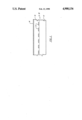
- the single FIGURE is a cross-section view of one embodiment of a solid state light modulator structure in accordance with the invention.
- a solid state light modulator 10 comprises a charge storage device including semiconductor substrate 12, such as silicon, including an array of charge storage elements (not shown) formed in the substrate, each charge storage element associated with at least one display electrode 14 on the substrate surface.
- a charge storage device may, for example, comprise a charge coupled device. A detailed description of the structure and operation of these devices is unnecessary to an understanding of this invention, and may be found, for example, in U.S. Pat. No. 3,882,271.
- a deformable elastomer layer 16 Disposed over the top of the charge storage element array is a deformable elastomer layer 16, herein a silica-containing gel.
- An adherent, light reflective metal electrode layer 18 is disposed on the top surface of elastomer lay 16, completing the light modulator.
- a charge array stored in the light modulator structure representing for example, a video frame
- Such deformation results in a rippled pattern on the surface of the gel and the light reflective layer 18, which pattern can then be "read” by reflecting light from the surface into a Schlieren optical system, which translates the pattern into a visual display image.
- Such an optical system and its operation are described in more detail in the above-referenced U.S. Pat. Nos. 4,626,920 and 3,882,271.
- the successful and efficient operation of the modulator structure is dependent upon the electrode layer 18 having sufficient flexibility and sufficient adherence to the gel surface so that it faithfully reproduces the deformations in the gel layer 16.
- the electrode layer 18 is preferably highly specularly reflective, so that the largest possible amount of light incident on the surface is reflected back into the optical system for display of the stored image.
- Such a layer is believed to result from a modification of the gel surface by the plasma present in the sputtering environment, by changing the crosslinking in the gel surface, and promoting a chemical reaction between the sputtered metal and the gel surface.
- the crosslinking is believed to make the gel surface more rigid, while the chemical reaction is believed to improve the bonding between the gel layer and the sputtered metal layer.
- the sputtering may be carried out over a wide range of operating conditions.
- the gas pressure may range from about 50 to about 200 micrometers, and the current may range from about 20 to about 500 milliamps.
- the sputtering deposition rate generally increases with increasing current, and the current increases with increasing gas pressure.
- a high deposition rate may result in undesirable heating of the substrate.
- deposition may be carried out in stages, with rest periods to allow cooling of the substrate to occur. In the alternative, provision may be made for actively cooling of the substrate in order to allow for continuous deposition.
- the gel layer should have a modulus of elasticity within a range to allow the required amount of deformation, which is determined by device geometry as well as the wavelength of the light to be modulated.
- red light having a wavelength of from about 550 to 570 nanometers may be modulated in a structure having a gel layer about 10 microns in thickness and having a modulus of elasticity between about 104 and 106 dynes per square centimeter.
- PDMS polydimethyl siloxanes
- a and B components where A is dimethylvinyl terminated polydimethyl siloxane and B is trimethyl terminated siloxane with partially hydrogen-substituted methyl side groups.
- These components are commercially available, for example, from the Dow Chemical Company under the tradename Dow Sylgard 527.
- Gels having various moduli of elasticity may be synthesized simply by varying the weight ratio of A to B. For example, varying the weight ratio of A:B from 1:1 to 1:2 results in a modulus of elasticity variation of approximately an order of magnitude.
- the modulus of elasticity may also be varied by changing the molecular weight of the A component, for example by washing or fractionation, and by changing the functionality of the B component, defined as the number of H side groups, for example, by the same techniques.
- Dow Sylgard 527 compounds were used for the synthesis of PDMS gels with A:B weight ratios of 1:1, 1:1.25, 1:1.5, 1:2, and 1:5.
- the average molecular weight distribution of both A and B components was broad and centered around 20,000 grams/mole.
- the components were mixed in the liquid state and formed into thin layers by spinning onto 17 ⁇ 17 millimeter monoscope substrates.
- Monoscopes were used instead of silicon semiconductor chips in order to enable study of the viscoelastic properties of the gels.
- the layers were gelled by curing them at a temperature of about 100° C. for a time of about one hour. The thickness of the cured layers was about 10 micrometers.
- Silver layers characterized as thick (about 1,000 angstroms) and thin (about 20 angstroms) were then sputtered onto the PDMS gel layers using sputtering conditions as follows: argon gas at a pressure of 160 micrometers, current at 200 milliamps, source-target distance at about 11/8 inch.
- the thick samples were produced by sputtering in pulses of 15 seconds duration, followed by 5 minutes of rest, while the thin samples were produced by a single pulse of less than 5 seconds duration.
- the silver thickness in the thin samples was determined by assuming a linear rate of silver deposition and extrapolating gravimetric measurements for the thick samples.
- a silver standard for X-ray photoelectron spectroscopy (XPS) was prepared by sputtering a thick silver layer onto a quartz substrate using the same sputtering conditions described above.
- a gel standard was prepared having an A:B ratio of 1:1.5 and having a surface free of any deposited metal.
- a gold standard was also formed by evaporating a thin gold layer on to a gel layer having an A:B ratio of 1:1.
- the thick silver layers obtained by sputtering are highly specular reflective (greater than 90 percent) and have a pale yellow color.
- XPS studies were conducted using a magnesium K.sub. ⁇ source at 300 watts with an analyzer including a triple detector having a resolution of 1.05 electron volts at 20 electron volts of pass energy, measured at the silver 3d 5/2 peak.
- the gold standard was assigned a peak value of 83.8 electron volts. The difference between this peak and the actual gold peak of 92.4 electron volts was assumed to be due to sample charging, and this value was used for assigning positions to the peaks in the silver samples.
- High resolution scans were then recorded in the vicinity of the silicon 2p, silicon 2s, carbon 1s, oxygen 1s, and silver 3d peaks, using 0.05 electron volt steps at 500 milliseconds per channel and a detector pass energy of 20 electron volts.
- the peak positions for the silver standard, the thin silver samples and the gel standard obtained from these scans are listed in Table I. All peak positions except the Auger peak positions were measured from the high resolution scans. The Auger peak positions were determined from the survey scans.
- Table I shows the silicon 2p, oxygen 1s, carbon 1s, and silver 3d 5/2 peak positions corrected for charging, and the Auger parameter for silver ( ⁇ ) for the thin samples, the silver standard and the gel standard.
- the variations in the peak positions are within experimental error except for the silver Auger parameter ⁇ which has shifted considerably (about 0.8 electron volts) in the thin samples, indicating a change in the chemical state of the silver sputtered on to the gel surfaces.
- the thick samples did not show such a shift in ⁇ , indicating that a chemical bond is formed between the sputtered silver and the gel surface at or near the gel-silver layer interface.
- the survey scans for both the thick and thin samples showed silicon 2p and other peaks associated with the gel structure, indicating that etching of the gel occurred during sputtering.
- Table II shows the ratios of the silver peak areas to the silicon, oxygen, and carbon peak areas for the thick and thin samples with varying ratios of A:B.
- the data for the thick samples indicates that the amount of etching depends upon the degree of gel crosslinking.
Abstract
A solid state light modulator structure useful in a video display system includes a deformable silica containing gel layer on an array of charge storage elements, and an adherent, highly light reflective metal (e.g., Ag) electrode layer formed directly on the surface of the gel layer by sputtering in a non-reactive atmosphere.
Description
This is a continuation of application Ser. No. 084,262, filed Aug. 11, 1987, now abandoned.
Co-pending U.S. patent application, Ser. No. 084,260, filed concurrently herewith, claims a method for metallizing a silica-containing gel, in which the gel surface is treated with an oxygen-containing plasma prior to metallization, and a solid state modulator incorporating the metallized gel.
This invention relates to a solid state light modulator structure useful in an apparatus for generating an image from a video input signal, and more particularly relates to such a structure including a deformable metallized elastomer layer, and also relates to a method for metallizing the layer.
U.S. Pat. No. 4,626,920 describes a video display system of the type employing solid state light modulator structures including a deformable, metallized elastomer layer. In this light modulator structure, the deformable layer, for example, a metallized silica-containing gel layer, is disposed over an array of electrodes on the surface of a solid state charge storage device, such as a charge coupled semiconductor device. The metal layer on the surface of the gel serves both as an electrode and as a light reflecting layer.
In operation, electric fields associated with the charge pattern of a stored video frame cause electrostatic attractions between the electrode array and the surface electrode, resulting in deformation of the gel layer in a pattern corresponding to the charge pattern. This pattern is analagous to a phase diffraction grating. The information contained in this pattern is then "read" by reflecting light from the deformed electrode into an optical subsystem such as a Schlieren type of optical system, which then translates the information into a viewable image on a screen.
A critical step in the formation of these light modulator structures is the formation of the light reflective electrode layer on the gel surface. In order for the device to operate successfully, such layer must be electrically conductive, flexible and adherent to the gel layer, and is preferably highly specularly reflective. Unfortunately, since gels are semisolids, having structures which may be characterized as having a liquid phase distributed in an open polymer network, they provide poor surfaces for adhesion.
In the referenced U.S. patent, an electrode layer with the desired characteristics is provided by first providing a thin pellicle layer of nitrocellulose on the gel surface, to provide a surface for adhesion, and to isolate the electrode layer from gel components which could attack and degrade it. Next, a thin intermediate layer of gold is evaporated onto the pellicle layer, followed by evaporation of a thin silver layer onto the gold layer. The gold layer enables the deposition of the silver layer with sufficient uniformity to result in a highly reflective layer.
While it would be desirable from the standpoint of manufacturing efficiency to eliminate the intermediate pellicle and gold layers, it has been found that the deposition of silver directly onto the gel surface by evaporation results in an extremely low specular reflectance, that is, less than one percent. G. C. Martin et al., J. Appl. Phys. 53 (1), 797 (1985).
Accordingly, it is a principal object of the invention to provide a solid state light modulator structure of the type described herein having an adherent, highly reflective metal layer on the surface of the gel layer.
It is another object of the invention to provide a method for forming an adherent, highly reflective metal layer directly onto a silica-containing gel surface without the need for forming intermediate or transitional layers.
In accordance with the invention, there is provided a solid state light modulator structure comprising:
(a) a solid state charge storage device comprising an array of charge storage elements formed in a semiconductor substrate, each element associated with at least one display electrode on the surface of the substrate,
(b) a deformable elastomer layer disposed on the surface of the charge storage device, the layer covering the array of display electrodes, and
(c) a flexible, adherent and light reflective conductive layer disposed over the elastomer layer,
characterized in that the elastomer layer is a silica-containing gel, the conductive layer is a metal layer, and the metal layer is bonded directly to the gel layer.
Such a solid state light modulator structure is further characterized in accordance with the invention in that the metal layer is selected from the group consisting of silver, aluminum and indium, and is preferably silver, having a specular reflectance of visible light of at least 90 percent.
In accordance with another aspect of the invention, there is provided a method for forming an adherent, light reflective metal layer directly onto the surface of a silica-containing gel, the method comprising sputtering the metal onto the gel surface in a nonreactive atmosphere such as an inert gas.
Such sputtered metal atoms arrive at the gel surface with much greater kinetic energy (one or more orders of magnitude greater) than if such atoms were evaporated. This high energy is thought to be responsible for the formation of a chemical bond between the metal atoms and silicon atoms at or near the gel-metal layer interface. The sputtered metal layer is thus adherent to the gel surface and highly reflective. Where the metal is silver, layers having specular reflectances greater than 90 percent are obtainable.
The single FIGURE is a cross-section view of one embodiment of a solid state light modulator structure in accordance with the invention.
In the FIGURE, a solid state light modulator 10 comprises a charge storage device including semiconductor substrate 12, such as silicon, including an array of charge storage elements (not shown) formed in the substrate, each charge storage element associated with at least one display electrode 14 on the substrate surface. Such a charge storage device may, for example, comprise a charge coupled device. A detailed description of the structure and operation of these devices is unnecessary to an understanding of this invention, and may be found, for example, in U.S. Pat. No. 3,882,271.
Disposed over the top of the charge storage element array is a deformable elastomer layer 16, herein a silica-containing gel. An adherent, light reflective metal electrode layer 18 is disposed on the top surface of elastomer lay 16, completing the light modulator.
In operation, a charge array stored in the light modulator structure representing for example, a video frame, in conjunction with a potential applied between the array of display electrodes and the upper light reflective electrode layer, results in a variation of potential across the gel layer 16, and electrostatic attraction forces between the electrode array 14 and the light reflective electrode 18, causing deformation of gel layer 16 and reflective layer 18. Such deformation results in a rippled pattern on the surface of the gel and the light reflective layer 18, which pattern can then be "read" by reflecting light from the surface into a Schlieren optical system, which translates the pattern into a visual display image. Such an optical system and its operation are described in more detail in the above-referenced U.S. Pat. Nos. 4,626,920 and 3,882,271.
As may be appreciated, the successful and efficient operation of the modulator structure is dependent upon the electrode layer 18 having sufficient flexibility and sufficient adherence to the gel surface so that it faithfully reproduces the deformations in the gel layer 16. In addition, the electrode layer 18 is preferably highly specularly reflective, so that the largest possible amount of light incident on the surface is reflected back into the optical system for display of the stored image.
However, attempts to simply evaporate a metal layer such as silver onto the surface of a silica-containing gel such as a polydimethyl siloxane (PDMS), results in poor adhesion to the surface and a very low specular reflectance (less than one percent). In accordance with the teachings of the invention, it has been discovered that forming the metal layer by sputtering in an inert gas such as argon results in a layer which is highly specularly reflective (greater than 90 percent in the case of silver) and which adheres well to the gel surface. Such a layer is believed to result from a modification of the gel surface by the plasma present in the sputtering environment, by changing the crosslinking in the gel surface, and promoting a chemical reaction between the sputtered metal and the gel surface. The crosslinking is believed to make the gel surface more rigid, while the chemical reaction is believed to improve the bonding between the gel layer and the sputtered metal layer.
The sputtering may be carried out over a wide range of operating conditions. For example, the gas pressure may range from about 50 to about 200 micrometers, and the current may range from about 20 to about 500 milliamps. As is known, the sputtering deposition rate generally increases with increasing current, and the current increases with increasing gas pressure. As is also known, a high deposition rate may result in undesirable heating of the substrate. In such cases, deposition may be carried out in stages, with rest periods to allow cooling of the substrate to occur. In the alternative, provision may be made for actively cooling of the substrate in order to allow for continuous deposition.
The gel layer should have a modulus of elasticity within a range to allow the required amount of deformation, which is determined by device geometry as well as the wavelength of the light to be modulated. By way of example, red light having a wavelength of from about 550 to 570 nanometers may be modulated in a structure having a gel layer about 10 microns in thickness and having a modulus of elasticity between about 104 and 106 dynes per square centimeter. When a field of about 50 volts is impressed across the gel layer between the electrode array on the surface of the semiconductor and the flexible metal electrode on the surface of the gel, an electrostatic attraction results in deformation of the gel by an amount of up to about 0.2 micrometers.
Particularly suitable for use as the gel layer in these structures are polydimethyl siloxanes (PDMS), which may be readily synthesized by curing a mixture of A and B components, where A is dimethylvinyl terminated polydimethyl siloxane and B is trimethyl terminated siloxane with partially hydrogen-substituted methyl side groups. These components are commercially available, for example, from the Dow Chemical Company under the tradename Dow Sylgard 527. Gels having various moduli of elasticity may be synthesized simply by varying the weight ratio of A to B. For example, varying the weight ratio of A:B from 1:1 to 1:2 results in a modulus of elasticity variation of approximately an order of magnitude. As is known, the modulus of elasticity may also be varied by changing the molecular weight of the A component, for example by washing or fractionation, and by changing the functionality of the B component, defined as the number of H side groups, for example, by the same techniques.
Dow Sylgard 527 compounds were used for the synthesis of PDMS gels with A:B weight ratios of 1:1, 1:1.25, 1:1.5, 1:2, and 1:5. The average molecular weight distribution of both A and B components was broad and centered around 20,000 grams/mole. The components were mixed in the liquid state and formed into thin layers by spinning onto 17×17 millimeter monoscope substrates. Monoscopes were used instead of silicon semiconductor chips in order to enable study of the viscoelastic properties of the gels. The layers were gelled by curing them at a temperature of about 100° C. for a time of about one hour. The thickness of the cured layers was about 10 micrometers.
Silver layers characterized as thick (about 1,000 angstroms) and thin (about 20 angstroms) were then sputtered onto the PDMS gel layers using sputtering conditions as follows: argon gas at a pressure of 160 micrometers, current at 200 milliamps, source-target distance at about 11/8 inch. The thick samples were produced by sputtering in pulses of 15 seconds duration, followed by 5 minutes of rest, while the thin samples were produced by a single pulse of less than 5 seconds duration. The silver thickness in the thin samples was determined by assuming a linear rate of silver deposition and extrapolating gravimetric measurements for the thick samples.
A silver standard for X-ray photoelectron spectroscopy (XPS) was prepared by sputtering a thick silver layer onto a quartz substrate using the same sputtering conditions described above. A gel standard was prepared having an A:B ratio of 1:1.5 and having a surface free of any deposited metal. A gold standard was also formed by evaporating a thin gold layer on to a gel layer having an A:B ratio of 1:1.
The thick silver layers obtained by sputtering are highly specular reflective (greater than 90 percent) and have a pale yellow color.
XPS studies were conducted using a magnesium K.sub.α source at 300 watts with an analyzer including a triple detector having a resolution of 1.05 electron volts at 20 electron volts of pass energy, measured at the silver 3d5/2 peak. The gold standard was assigned a peak value of 83.8 electron volts. The difference between this peak and the actual gold peak of 92.4 electron volts was assumed to be due to sample charging, and this value was used for assigning positions to the peaks in the silver samples.
Survey scans of both the thick and thin silver samples were conducted at low (from about 5 to 605 electron volts) and high (from about 600 to 1200 electron volts) binding energy, using 0.2 electron volt steps at 500 milliseconds per channel and a detector pass energy of 50 electron volts.
High resolution scans were then recorded in the vicinity of the silicon 2p, silicon 2s, carbon 1s, oxygen 1s, and silver 3d peaks, using 0.05 electron volt steps at 500 milliseconds per channel and a detector pass energy of 20 electron volts. The peak positions for the silver standard, the thin silver samples and the gel standard obtained from these scans are listed in Table I. All peak positions except the Auger peak positions were measured from the high resolution scans. The Auger peak positions were determined from the survey scans.
                                  TABLE I
__________________________________________________________________________
      Silver                   Gel
Element
      Standard
           1:1 1:1.25
                   1:1.5
                       1:2 1:5 Standard
__________________________________________________________________________
Si 2p --   102.10
               102.05
                   102.10
                       102.10
                           102.00
                               102.20
O 1s  --   532.05
               532.00
                   532.00
                       532.10
                           532.00
                               532.30
C 1s  --   284.45
               284.35
                   284.45
                       284.45
                           284.35
                               284.50
Ag 3d 5/2
      368.10
           367.85
               367.85
                   367.90
                       367.90
                           367.85
                               --
Ag α
      527.6
           528.4
               528.5
                   528.4
                       528.3
                           528.2
                               --
__________________________________________________________________________
Table I shows the silicon 2p, oxygen 1s, carbon 1s, and silver 3d5/2 peak positions corrected for charging, and the Auger parameter for silver (α) for the thin samples, the silver standard and the gel standard. The variations in the peak positions are within experimental error except for the silver Auger parameter α which has shifted considerably (about 0.8 electron volts) in the thin samples, indicating a change in the chemical state of the silver sputtered on to the gel surfaces. The thick samples did not show such a shift in α, indicating that a chemical bond is formed between the sputtered silver and the gel surface at or near the gel-silver layer interface.
Areas under the peaks on the survey scans were measured, and the ratios of the areas under the silver peaks to the areas under the peaks for silicon, oxygen and carbon were computed. These ratios are listed in Table II for the thick and thin silver samples.
              TABLE II
______________________________________
A to B              Ag/                           Ag/
Ratio O      Ag     O    C    Ag   Ag/C  Si  Ag   Si
______________________________________
Silver Thickness (A) 20
1:1   19.5   80.5   4.1  18.0 82.0 4.6   4.4 95.6 21.6
1:1.25
      16.5   83.5   5.1  15.0 85.0 5.7   4.3 95.7 22.4
1:1.5 15.6   84.4   5.4  16.2 83.8 5.2   4.3 95.7 22.1
1:2   17.8   82.2   4.6  15.9 84.1 5.3   4.7 95.3 20.2
1:5   14.3   85.7   6.0  15.7 84.3 5.4   3.5 96.5 28.0
______________________________________
Silver Thickness (A) 1000
1:1   16.2   84.8   5.2  11.3 88.7 7.9   4.8 95.2 19.8
1:1.25
      11.8   88.2   7.5  7.4  92.6 12.6  2.5 97.5 39.0
1:1.5 10.7   89.3   8.3  8.0  92.0 11.5  1.2 98.8 81.0
1:2   13.2   86.8   6.6  8.6  91.4 10.6  2.9 97.1 33.8
1:5   15.9   84.1   5.3  11.0 89.0 8.1   4.2 95.8 22.6
______________________________________
The survey scans for both the thick and thin samples showed silicon 2p and other peaks associated with the gel structure, indicating that etching of the gel occurred during sputtering.
Table II shows the ratios of the silver peak areas to the silicon, oxygen, and carbon peak areas for the thick and thin samples with varying ratios of A:B. The data for the thick samples indicates that the amount of etching depends upon the degree of gel crosslinking. The peak area ratios of the thick samples reaches a maximum (silver/silicon=81.0) for the A:B ratio of 1:1.5, apparently indicating that the etch rate is slower in the 1:1.5 samples and faster in the 1:1 and 1:5 samples, with the etch rates of these latter samples being approximately the same.
While there have been shown and described what are at present considered to be the preferred embodiments of the invention, it will be apparent to those skilled in the art that various changes and modifications may be made therein without departing from the scope of the invention as defined by the appended claims.
Claims (4)
1. A solid state light modulator structure comprising:
(a) a solid state charge storage device comprising an array of charge storage elements formed in a semiconductor substrate, each element associated with at least one display electrode on the surface of the substrate,
(b) a deformable elastomer layer disposed on the solid state device, the layer covering the electrode array, and
(c) a flexible, adherent and light reflective conductive layer disposed over the elastomer layer,
characterized in that the elastomer layer is polydimethyl siloxane gel, the conductive layer consists of a single sputtered metal layer, and the metal layer is bonded directly to the gel layer.
2. The solid state light modulator of claim 1 in which the metal in the conductive metal layer is selected from the group consisting of silver, aluminum and indium.
3. The solid state light modulator of claim 2 in which the metal is silver.
4. The solid state light modulator of claim 3 in which the specular reflectance of the silver layer is at least 90 percent.
Priority Applications (1)
| Application Number | Priority Date | Filing Date | Title |
|---|---|---|---|
| US07/292,632 US4900136A (en) | 1987-08-11 | 1988-10-28 | Method of metallizing silica-containing gel and solid state light modulator incorporating the metallized gel |
Applications Claiming Priority (2)
| Application Number | Priority Date | Filing Date | Title |
|---|---|---|---|
| US8426287A | 1987-08-11 | 1987-08-11 | |
| US07/292,632 US4900136A (en) | 1987-08-11 | 1988-10-28 | Method of metallizing silica-containing gel and solid state light modulator incorporating the metallized gel |
Related Parent Applications (1)
| Application Number | Title | Priority Date | Filing Date |
|---|---|---|---|
| US8426287A Continuation | 1987-08-11 | 1987-08-11 |
Related Child Applications (1)
| Application Number | Title | Priority Date | Filing Date |
|---|---|---|---|
| US41039489A Continuation | 1987-08-11 | 1989-09-20 |
Publications (1)
| Publication Number | Publication Date |
|---|---|
| US4900136A true US4900136A (en) | 1990-02-13 |
Family
ID=26770769
Family Applications (1)
| Application Number | Title | Priority Date | Filing Date |
|---|---|---|---|
| US07/292,632 Expired - Fee Related US4900136A (en) | 1987-08-11 | 1988-10-28 | Method of metallizing silica-containing gel and solid state light modulator incorporating the metallized gel |
Country Status (1)
| Country | Link |
|---|---|
| US (1) | US4900136A (en) |
Cited By (133)
| Publication number | Priority date | Publication date | Assignee | Title |
|---|---|---|---|---|
| US5517348A (en) * | 1994-10-27 | 1996-05-14 | Motorola | Voltage controlled transparent layer for a bi-directinal device |
| US5521746A (en) * | 1993-02-22 | 1996-05-28 | Engle; Craig D. | Poppet valve modulator |
| US20020075555A1 (en) * | 1994-05-05 | 2002-06-20 | Iridigm Display Corporation | Interferometric modulation of radiation |
| US6639710B2 (en) * | 2001-09-19 | 2003-10-28 | Lucent Technologies Inc. | Method and apparatus for the correction of optical signal wave front distortion using adaptive optics |
| US6710908B2 (en) * | 1994-05-05 | 2004-03-23 | Iridigm Display Corporation | Controlling micro-electro-mechanical cavities |
| US20040058532A1 (en) * | 2002-09-20 | 2004-03-25 | Miles Mark W. | Controlling electromechanical behavior of structures within a microelectromechanical systems device |
| US20040130773A1 (en) * | 2002-09-06 | 2004-07-08 | Anders Malthe-Sorenssen | Method and device for variable optical attenuator |
| US20050036095A1 (en) * | 2003-08-15 | 2005-02-17 | Jia-Jiun Yeh | Color-changeable pixels of an optical interference display panel |
| US20050046922A1 (en) * | 2003-09-03 | 2005-03-03 | Wen-Jian Lin | Interferometric modulation pixels and manufacturing method thereof |
| US20050070768A1 (en) * | 2003-09-30 | 2005-03-31 | Qingsheng Zhu | Sensors having protective eluting coating and method therefor |
| US20050078348A1 (en) * | 2003-09-30 | 2005-04-14 | Wen-Jian Lin | Structure of a micro electro mechanical system and the manufacturing method thereof |
| US20050122560A1 (en) * | 2003-12-09 | 2005-06-09 | Sampsell Jeffrey B. | Area array modulation and lead reduction in interferometric modulators |
| US20050195467A1 (en) * | 2004-03-03 | 2005-09-08 | Manish Kothari | Altering temporal response of microelectromechanical elements |
| US20050231790A1 (en) * | 1994-05-05 | 2005-10-20 | Miles Mark W | Method and device for modulating light with a time-varying signal |
| US20050249966A1 (en) * | 2004-05-04 | 2005-11-10 | Ming-Hau Tung | Method of manufacture for microelectromechanical devices |
| US20050250235A1 (en) * | 2002-09-20 | 2005-11-10 | Miles Mark W | Controlling electromechanical behavior of structures within a microelectromechanical systems device |
| US20060007517A1 (en) * | 2004-07-09 | 2006-01-12 | Prime View International Co., Ltd. | Structure of a micro electro mechanical system |
| US20060006138A1 (en) * | 2003-08-26 | 2006-01-12 | Wen-Jian Lin | Interference display cell and fabrication method thereof |
| US20060024880A1 (en) * | 2004-07-29 | 2006-02-02 | Clarence Chui | System and method for micro-electromechanical operation of an interferometric modulator |
| US20060033975A1 (en) * | 1995-05-01 | 2006-02-16 | Miles Mark W | Photonic MEMS and structures |
| US20060067643A1 (en) * | 2004-09-27 | 2006-03-30 | Clarence Chui | System and method for multi-level brightness in interferometric modulation |
| US20060066504A1 (en) * | 2004-09-27 | 2006-03-30 | Sampsell Jeffrey B | System with server based control of client device display features |
| US20060066595A1 (en) * | 2004-09-27 | 2006-03-30 | Sampsell Jeffrey B | Method and system for driving a bi-stable display |
| US20060067651A1 (en) * | 2004-09-27 | 2006-03-30 | Clarence Chui | Photonic MEMS and structures |
| US20060065366A1 (en) * | 2004-09-27 | 2006-03-30 | Cummings William J | Portable etch chamber |
| US20060067646A1 (en) * | 2004-09-27 | 2006-03-30 | Clarence Chui | MEMS device fabricated on a pre-patterned substrate |
| US20060066503A1 (en) * | 2004-09-27 | 2006-03-30 | Sampsell Jeffrey B | Controller and driver features for bi-stable display |
| US20060067644A1 (en) * | 2004-09-27 | 2006-03-30 | Clarence Chui | Method of fabricating interferometric devices using lift-off processing techniques |
| US20060065940A1 (en) * | 2004-09-27 | 2006-03-30 | Manish Kothari | Analog interferometric modulator device |
| US20060066596A1 (en) * | 2004-09-27 | 2006-03-30 | Sampsell Jeffrey B | System and method of transmitting video data |
| US20060066599A1 (en) * | 2004-09-27 | 2006-03-30 | Clarence Chui | Reflective display pixels arranged in non-rectangular arrays |
| US20060066543A1 (en) * | 2004-09-27 | 2006-03-30 | Gally Brian J | Ornamental display device |
| US20060065622A1 (en) * | 2004-09-27 | 2006-03-30 | Floyd Philip D | Method and system for xenon fluoride etching with enhanced efficiency |
| US20060066932A1 (en) * | 2004-09-27 | 2006-03-30 | Clarence Chui | Method of selective etching using etch stop layer |
| US20060067649A1 (en) * | 2004-09-27 | 2006-03-30 | Ming-Hau Tung | Apparatus and method for reducing slippage between structures in an interferometric modulator |
| US20060067650A1 (en) * | 2004-09-27 | 2006-03-30 | Clarence Chui | Method of making a reflective display device using thin film transistor production techniques |
| US20060066876A1 (en) * | 2004-09-27 | 2006-03-30 | Manish Kothari | Method and system for sensing light using interferometric elements |
| US20060077504A1 (en) * | 2004-09-27 | 2006-04-13 | Floyd Philip D | Method and device for protecting interferometric modulators from electrostatic discharge |
| US20060079048A1 (en) * | 2004-09-27 | 2006-04-13 | Sampsell Jeffrey B | Method of making prestructure for MEMS systems |
| US20060077502A1 (en) * | 2004-09-27 | 2006-04-13 | Ming-Hau Tung | Methods of fabricating interferometric modulators by selectively removing a material |
| US20060077156A1 (en) * | 2004-09-27 | 2006-04-13 | Clarence Chui | MEMS device having deformable membrane characterized by mechanical persistence |
| US20060077521A1 (en) * | 2004-09-27 | 2006-04-13 | Gally Brian J | System and method of implementation of interferometric modulators for display mirrors |
| US20060077516A1 (en) * | 2004-09-27 | 2006-04-13 | Manish Kothari | Device having a conductive light absorbing mask and method for fabricating same |
| US20060077519A1 (en) * | 2004-09-27 | 2006-04-13 | Floyd Philip D | System and method for providing thermal compensation for an interferometric modulator display |
| US20060077518A1 (en) * | 2004-09-27 | 2006-04-13 | Clarence Chui | Mirror and mirror layer for optical modulator and method |
| US20060077617A1 (en) * | 2004-09-27 | 2006-04-13 | Floyd Philip D | Selectable capacitance circuit |
| US20060077155A1 (en) * | 2004-09-27 | 2006-04-13 | Clarence Chui | Reflective display device having viewable display on both sides |
| US20060077527A1 (en) * | 2004-09-27 | 2006-04-13 | Cummings William J | Methods and devices for inhibiting tilting of a mirror in an interferometric modulator |
| US20060077515A1 (en) * | 2004-09-27 | 2006-04-13 | Cummings William J | Method and device for corner interferometric modulation |
| US20060077151A1 (en) * | 2004-09-27 | 2006-04-13 | Clarence Chui | Method and device for a display having transparent components integrated therein |
| US20060077528A1 (en) * | 2004-09-27 | 2006-04-13 | Floyd Philip D | Device and method for modifying actuation voltage thresholds of a deformable membrane in an interferometric modulator |
| US20060077508A1 (en) * | 2004-09-27 | 2006-04-13 | Clarence Chui | Method and device for multistate interferometric light modulation |
| US20060077507A1 (en) * | 2004-09-27 | 2006-04-13 | Clarence Chui | Conductive bus structure for interferometric modulator array |
| US20060077152A1 (en) * | 2004-09-27 | 2006-04-13 | Clarence Chui | Device and method for manipulation of thermal response in a modulator |
| US20060177950A1 (en) * | 2005-02-04 | 2006-08-10 | Wen-Jian Lin | Method of manufacturing optical interferance color display |
| US20060176241A1 (en) * | 2004-09-27 | 2006-08-10 | Sampsell Jeffrey B | System and method of transmitting video data |
| US7126738B2 (en) | 1995-05-01 | 2006-10-24 | Idc, Llc | Visible spectrum modulator arrays |
| US20060257070A1 (en) * | 2003-05-26 | 2006-11-16 | Wen-Jian Lin | Optical interference display cell and method of making the same |
| US20060256420A1 (en) * | 2003-06-24 | 2006-11-16 | Miles Mark W | Film stack for manufacturing micro-electromechanical systems (MEMS) devices |
| US7138984B1 (en) | 2001-06-05 | 2006-11-21 | Idc, Llc | Directly laminated touch sensitive screen |
| US20060262380A1 (en) * | 1998-04-08 | 2006-11-23 | Idc, Llc A Delaware Limited Liability Company | MEMS devices with stiction bumps |
| US20060274074A1 (en) * | 1994-05-05 | 2006-12-07 | Miles Mark W | Display device having a movable structure for modulating light and method thereof |
| US20070019922A1 (en) * | 2005-07-22 | 2007-01-25 | Teruo Sasagawa | Support structure for MEMS device and methods therefor |
| US7172915B2 (en) | 2003-01-29 | 2007-02-06 | Qualcomm Mems Technologies Co., Ltd. | Optical-interference type display panel and method for making the same |
| US20070058095A1 (en) * | 1994-05-05 | 2007-03-15 | Miles Mark W | System and method for charge control in a MEMS device |
| US20070096300A1 (en) * | 2005-10-28 | 2007-05-03 | Hsin-Fu Wang | Diffusion barrier layer for MEMS devices |
| US20070097134A1 (en) * | 1994-05-05 | 2007-05-03 | Miles Mark W | Systems and methods of testing micro-electromechanical devices |
| US20070155051A1 (en) * | 2005-12-29 | 2007-07-05 | Chun-Ming Wang | Method of creating MEMS device cavities by a non-etching process |
| US20070170540A1 (en) * | 2006-01-18 | 2007-07-26 | Chung Won Suk | Silicon-rich silicon nitrides as etch stops in MEMS manufature |
| US7250315B2 (en) | 2002-02-12 | 2007-07-31 | Idc, Llc | Method for fabricating a structure for a microelectromechanical system (MEMS) device |
| US20070189654A1 (en) * | 2006-01-13 | 2007-08-16 | Lasiter Jon B | Interconnect structure for MEMS device |
| US20070196944A1 (en) * | 2006-02-22 | 2007-08-23 | Chen-Jean Chou | Electrical conditioning of MEMS device and insulating layer thereof |
| US20070194630A1 (en) * | 2006-02-23 | 2007-08-23 | Marc Mignard | MEMS device having a layer movable at asymmetric rates |
| US20070194414A1 (en) * | 2006-02-21 | 2007-08-23 | Chen-Jean Chou | Method for providing and removing discharging interconnect for chip-on-glass output leads and structures thereof |
| US20070206267A1 (en) * | 2006-03-02 | 2007-09-06 | Ming-Hau Tung | Methods for producing MEMS with protective coatings using multi-component sacrificial layers |
| US20070236774A1 (en) * | 2006-04-10 | 2007-10-11 | Evgeni Gousev | Interferometric optical display system with broadband characteristics |
| US20070242008A1 (en) * | 2006-04-17 | 2007-10-18 | William Cummings | Mode indicator for interferometric modulator displays |
| US20070249079A1 (en) * | 2006-04-19 | 2007-10-25 | Teruo Sasagawa | Non-planar surface structures and process for microelectromechanical systems |
| US20070247401A1 (en) * | 2006-04-19 | 2007-10-25 | Teruo Sasagawa | Microelectromechanical device and method utilizing nanoparticles |
| US20070247696A1 (en) * | 2006-04-19 | 2007-10-25 | Teruo Sasagawa | Microelectromechanical device and method utilizing a porous surface |
| US20070249078A1 (en) * | 2006-04-19 | 2007-10-25 | Ming-Hau Tung | Non-planar surface structures and process for microelectromechanical systems |
| US20070258123A1 (en) * | 2006-05-03 | 2007-11-08 | Gang Xu | Electrode and interconnect materials for MEMS devices |
| US7297471B1 (en) | 2003-04-15 | 2007-11-20 | Idc, Llc | Method for manufacturing an array of interferometric modulators |
| US20070279730A1 (en) * | 2006-06-01 | 2007-12-06 | David Heald | Process and structure for fabrication of mems device having isolated egde posts |
| US20070279753A1 (en) * | 2006-06-01 | 2007-12-06 | Ming-Hau Tung | Patterning of mechanical layer in MEMS to reduce stresses at supports |
| US20070279729A1 (en) * | 2006-06-01 | 2007-12-06 | Manish Kothari | Analog interferometric modulator device with electrostatic actuation and release |
| US20080003710A1 (en) * | 2006-06-28 | 2008-01-03 | Lior Kogut | Support structure for free-standing MEMS device and methods for forming the same |
| US20080003737A1 (en) * | 2006-06-30 | 2008-01-03 | Ming-Hau Tung | Method of manufacturing MEMS devices providing air gap control |
| US7327510B2 (en) | 2004-09-27 | 2008-02-05 | Idc, Llc | Process for modifying offset voltage characteristics of an interferometric modulator |
| US20080032439A1 (en) * | 2006-08-02 | 2008-02-07 | Xiaoming Yan | Selective etching of MEMS using gaseous halides and reactive co-etchants |
| US20080037093A1 (en) * | 1994-05-05 | 2008-02-14 | Idc, Llc | Method and device for multi-color interferometric modulation |
| US20080036795A1 (en) * | 1994-05-05 | 2008-02-14 | Idc, Llc | Method and device for modulating light |
| US20080043315A1 (en) * | 2006-08-15 | 2008-02-21 | Cummings William J | High profile contacts for microelectromechanical systems |
| US20080055707A1 (en) * | 2006-06-28 | 2008-03-06 | Lior Kogut | Support structure for free-standing MEMS device and methods for forming the same |
| US20080088910A1 (en) * | 1994-05-05 | 2008-04-17 | Idc, Llc | System and method for a mems device |
| US20080088908A1 (en) * | 1994-05-05 | 2008-04-17 | Idc, Llc | System and method for a mems device |
| US20080088912A1 (en) * | 1994-05-05 | 2008-04-17 | Idc, Llc | System and method for a mems device |
| US20080094686A1 (en) * | 2006-10-19 | 2008-04-24 | U Ren Gregory David | Sacrificial spacer process and resultant structure for MEMS support structure |
| US20080279498A1 (en) * | 2007-05-11 | 2008-11-13 | Qualcomm Incorporated | Mems structures, methods of fabricating mems components on separate substrates and assembly of same |
| US7460291B2 (en) | 1994-05-05 | 2008-12-02 | Idc, Llc | Separable modulator |
| EP2000828A2 (en) | 1999-12-23 | 2008-12-10 | Longevyty AS | Optical systems |
| US20080310008A1 (en) * | 2007-06-14 | 2008-12-18 | Qualcomm Incorporated | Method of patterning mechanical layer for mems structures |
| US7471444B2 (en) | 1996-12-19 | 2008-12-30 | Idc, Llc | Interferometric modulation of radiation |
| US7471442B2 (en) | 2006-06-15 | 2008-12-30 | Qualcomm Mems Technologies, Inc. | Method and apparatus for low range bit depth enhancements for MEMS display architectures |
| US20090009444A1 (en) * | 2007-07-03 | 2009-01-08 | Qualcomm Incorporated | Mems devices having improved uniformity and methods for making them |
| US7486867B2 (en) | 2005-08-19 | 2009-02-03 | Qualcomm Mems Technologies, Inc. | Methods for forming layers within a MEMS device using liftoff processes to achieve a tapered edge |
| US7492502B2 (en) | 2004-09-27 | 2009-02-17 | Idc, Llc | Method of fabricating a free-standing microstructure |
| US7527996B2 (en) | 2006-04-19 | 2009-05-05 | Qualcomm Mems Technologies, Inc. | Non-planar surface structures and process for microelectromechanical systems |
| US7532377B2 (en) | 1998-04-08 | 2009-05-12 | Idc, Llc | Movable micro-electromechanical device |
| US7535621B2 (en) | 2006-12-27 | 2009-05-19 | Qualcomm Mems Technologies, Inc. | Aluminum fluoride films for microelectromechanical system applications |
| US7566940B2 (en) | 2005-07-22 | 2009-07-28 | Qualcomm Mems Technologies, Inc. | Electromechanical devices having overlying support structures |
| US20090257113A1 (en) * | 2006-06-01 | 2009-10-15 | Light Resonance Technologies, Llc | Light filter/modulator and array of filters/modulators |
| US20100039370A1 (en) * | 1996-12-19 | 2010-02-18 | Idc, Llc | Method of making a light modulating display device and associated transistor circuitry and structures thereof |
| US7684104B2 (en) | 2004-09-27 | 2010-03-23 | Idc, Llc | MEMS using filler material and method |
| US7706042B2 (en) | 2006-12-20 | 2010-04-27 | Qualcomm Mems Technologies, Inc. | MEMS device and interconnects for same |
| US7738157B2 (en) | 1994-05-05 | 2010-06-15 | Qualcomm Mems Technologies, Inc. | System and method for a MEMS device |
| US7763546B2 (en) | 2006-08-02 | 2010-07-27 | Qualcomm Mems Technologies, Inc. | Methods for reducing surface charges during the manufacture of microelectromechanical systems devices |
| US7776631B2 (en) | 1994-05-05 | 2010-08-17 | Qualcomm Mems Technologies, Inc. | MEMS device and method of forming a MEMS device |
| US20100245980A1 (en) * | 1996-11-05 | 2010-09-30 | Qualcomm Mems Technologies, Inc. | System and method for a mems device |
| US7808703B2 (en) | 2004-09-27 | 2010-10-05 | Qualcomm Mems Technologies, Inc. | System and method for implementation of interferometric modulator displays |
| US7808694B2 (en) | 1994-05-05 | 2010-10-05 | Qualcomm Mems Technologies, Inc. | Method and device for modulating light |
| US7830587B2 (en) | 1993-03-17 | 2010-11-09 | Qualcomm Mems Technologies, Inc. | Method and device for modulating light with semiconductor substrate |
| US7863079B2 (en) | 2008-02-05 | 2011-01-04 | Qualcomm Mems Technologies, Inc. | Methods of reducing CD loss in a microelectromechanical device |
| USRE42119E1 (en) | 2002-02-27 | 2011-02-08 | Qualcomm Mems Technologies, Inc. | Microelectrochemical systems device and method for fabricating same |
| US7893919B2 (en) | 2004-09-27 | 2011-02-22 | Qualcomm Mems Technologies, Inc. | Display region architectures |
| US7898722B2 (en) | 1995-05-01 | 2011-03-01 | Qualcomm Mems Technologies, Inc. | Microelectromechanical device with restoring electrode |
| US8659816B2 (en) | 2011-04-25 | 2014-02-25 | Qualcomm Mems Technologies, Inc. | Mechanical layer and methods of making the same |
| US8817357B2 (en) | 2010-04-09 | 2014-08-26 | Qualcomm Mems Technologies, Inc. | Mechanical layer and methods of forming the same |
| US8885244B2 (en) | 2004-09-27 | 2014-11-11 | Qualcomm Mems Technologies, Inc. | Display device |
| US8928967B2 (en) | 1998-04-08 | 2015-01-06 | Qualcomm Mems Technologies, Inc. | Method and device for modulating light |
| US8963159B2 (en) | 2011-04-04 | 2015-02-24 | Qualcomm Mems Technologies, Inc. | Pixel via and methods of forming the same |
| US9001412B2 (en) | 2004-09-27 | 2015-04-07 | Qualcomm Mems Technologies, Inc. | Electromechanical device with optical function separated from mechanical and electrical function |
| US9134527B2 (en) | 2011-04-04 | 2015-09-15 | Qualcomm Mems Technologies, Inc. | Pixel via and methods of forming the same |
Citations (8)
| Publication number | Priority date | Publication date | Assignee | Title |
|---|---|---|---|---|
| US3907407A (en) * | 1973-10-29 | 1975-09-23 | Rca Corp | Elastic light-scattering modulator device |
| US3980476A (en) * | 1975-01-27 | 1976-09-14 | Xerox Corporation | Imaging system |
| US4013345A (en) * | 1975-10-22 | 1977-03-22 | Rca Corporation | Deformable mirror light valve and method of operating the same |
| US4294507A (en) * | 1980-01-25 | 1981-10-13 | International Business Machines Corporation | Controllably deformed elastic waveguide elements |
| US4299450A (en) * | 1978-08-18 | 1981-11-10 | Sharp Kabushiki Kaisha | Elastomer display |
| US4485066A (en) * | 1983-02-08 | 1984-11-27 | International Business Machines Corporation | Method of making elastomer-coated hot roll |
| US4494826A (en) * | 1979-12-31 | 1985-01-22 | Smith James L | Surface deformation image device |
| US4626920A (en) * | 1984-01-30 | 1986-12-02 | New York Institute Of Technology | Solid state light modulator structure |
-
1988
- 1988-10-28 US US07/292,632 patent/US4900136A/en not_active Expired - Fee Related
Patent Citations (8)
| Publication number | Priority date | Publication date | Assignee | Title |
|---|---|---|---|---|
| US3907407A (en) * | 1973-10-29 | 1975-09-23 | Rca Corp | Elastic light-scattering modulator device |
| US3980476A (en) * | 1975-01-27 | 1976-09-14 | Xerox Corporation | Imaging system |
| US4013345A (en) * | 1975-10-22 | 1977-03-22 | Rca Corporation | Deformable mirror light valve and method of operating the same |
| US4299450A (en) * | 1978-08-18 | 1981-11-10 | Sharp Kabushiki Kaisha | Elastomer display |
| US4494826A (en) * | 1979-12-31 | 1985-01-22 | Smith James L | Surface deformation image device |
| US4294507A (en) * | 1980-01-25 | 1981-10-13 | International Business Machines Corporation | Controllably deformed elastic waveguide elements |
| US4485066A (en) * | 1983-02-08 | 1984-11-27 | International Business Machines Corporation | Method of making elastomer-coated hot roll |
| US4626920A (en) * | 1984-01-30 | 1986-12-02 | New York Institute Of Technology | Solid state light modulator structure |
Cited By (278)
| Publication number | Priority date | Publication date | Assignee | Title |
|---|---|---|---|---|
| US5521746A (en) * | 1993-02-22 | 1996-05-28 | Engle; Craig D. | Poppet valve modulator |
| US7830587B2 (en) | 1993-03-17 | 2010-11-09 | Qualcomm Mems Technologies, Inc. | Method and device for modulating light with semiconductor substrate |
| US20070058095A1 (en) * | 1994-05-05 | 2007-03-15 | Miles Mark W | System and method for charge control in a MEMS device |
| US7826120B2 (en) | 1994-05-05 | 2010-11-02 | Qualcomm Mems Technologies, Inc. | Method and device for multi-color interferometric modulation |
| US8105496B2 (en) | 1994-05-05 | 2012-01-31 | Qualcomm Mems Technologies, Inc. | Method of fabricating MEMS devices (such as IMod) comprising using a gas phase etchant to remove a layer |
| US6710908B2 (en) * | 1994-05-05 | 2004-03-23 | Iridigm Display Corporation | Controlling micro-electro-mechanical cavities |
| US20070253054A1 (en) * | 1994-05-05 | 2007-11-01 | Miles Mark W | Display devices comprising of interferometric modulator and sensor |
| US8081369B2 (en) | 1994-05-05 | 2011-12-20 | Qualcomm Mems Technologies, Inc. | System and method for a MEMS device |
| US8059326B2 (en) | 1994-05-05 | 2011-11-15 | Qualcomm Mems Technologies Inc. | Display devices comprising of interferometric modulator and sensor |
| US8035884B2 (en) | 1994-05-05 | 2011-10-11 | Qualcomm Mems Technologies, Inc. | Method and device for modulating light with semiconductor substrate |
| US7776631B2 (en) | 1994-05-05 | 2010-08-17 | Qualcomm Mems Technologies, Inc. | MEMS device and method of forming a MEMS device |
| US20100220248A1 (en) * | 1994-05-05 | 2010-09-02 | Qualcomm Mems Technologies, Inc. | Projection display |
| US8014059B2 (en) | 1994-05-05 | 2011-09-06 | Qualcomm Mems Technologies, Inc. | System and method for charge control in a MEMS device |
| US20110043891A1 (en) * | 1994-05-05 | 2011-02-24 | Qualcomm Mems Technologies, Inc. | Method for modulating light |
| US7738157B2 (en) | 1994-05-05 | 2010-06-15 | Qualcomm Mems Technologies, Inc. | System and method for a MEMS device |
| US20050231790A1 (en) * | 1994-05-05 | 2005-10-20 | Miles Mark W | Method and device for modulating light with a time-varying signal |
| US20050244949A1 (en) * | 1994-05-05 | 2005-11-03 | Miles Mark W | Method and device for modulating light |
| US7800809B2 (en) | 1994-05-05 | 2010-09-21 | Qualcomm Mems Technologies, Inc. | System and method for a MEMS device |
| US7280265B2 (en) | 1994-05-05 | 2007-10-09 | Idc, Llc | Interferometric modulation of radiation |
| US20070229936A1 (en) * | 1994-05-05 | 2007-10-04 | Idc, Llc | Method of making a light modulating display device and associated transistor circuitry and structures thereof |
| US20080037093A1 (en) * | 1994-05-05 | 2008-02-14 | Idc, Llc | Method and device for multi-color interferometric modulation |
| US7460291B2 (en) | 1994-05-05 | 2008-12-02 | Idc, Llc | Separable modulator |
| US20060028708A1 (en) * | 1994-05-05 | 2006-02-09 | Miles Mark W | Method and device for modulating light |
| US7463421B2 (en) | 1994-05-05 | 2008-12-09 | Idc, Llc | Method and device for modulating light |
| US7012732B2 (en) | 1994-05-05 | 2006-03-14 | Idc, Llc | Method and device for modulating light with a time-varying signal |
| US7692844B2 (en) | 1994-05-05 | 2010-04-06 | Qualcomm Mems Technologies, Inc. | Interferometric modulation of radiation |
| US20020126364A1 (en) * | 1994-05-05 | 2002-09-12 | Iridigm Display Corporation, A Delaware Corporation | Interferometric modulation of radiation |
| US20080036795A1 (en) * | 1994-05-05 | 2008-02-14 | Idc, Llc | Method and device for modulating light |
| US7808694B2 (en) | 1994-05-05 | 2010-10-05 | Qualcomm Mems Technologies, Inc. | Method and device for modulating light |
| US7372619B2 (en) | 1994-05-05 | 2008-05-13 | Idc, Llc | Display device having a movable structure for modulating light and method thereof |
| US7619810B2 (en) | 1994-05-05 | 2009-11-17 | Idc, Llc | Systems and methods of testing micro-electromechanical devices |
| US20080084601A1 (en) * | 1994-05-05 | 2008-04-10 | Idc, Llc. | System and method for a mems device |
| US20020075555A1 (en) * | 1994-05-05 | 2002-06-20 | Iridigm Display Corporation | Interferometric modulation of radiation |
| US7042643B2 (en) | 1994-05-05 | 2006-05-09 | Idc, Llc | Interferometric modulation of radiation |
| US20080088910A1 (en) * | 1994-05-05 | 2008-04-17 | Idc, Llc | System and method for a mems device |
| US7839556B2 (en) | 1994-05-05 | 2010-11-23 | Qualcomm Mems Technologies, Inc. | Method and device for modulating light |
| US20070097134A1 (en) * | 1994-05-05 | 2007-05-03 | Miles Mark W | Systems and methods of testing micro-electromechanical devices |
| US7848001B2 (en) | 1994-05-05 | 2010-12-07 | Qualcomm Mems Technologies, Inc. | Method and system for interferometric modulation in projection or peripheral devices |
| US20080088908A1 (en) * | 1994-05-05 | 2008-04-17 | Idc, Llc | System and method for a mems device |
| US7846344B2 (en) | 1994-05-05 | 2010-12-07 | Qualcomm Mems Technologies, Inc. | Method and device for modulating light |
| US7848004B2 (en) | 1994-05-05 | 2010-12-07 | Qualcomm Mems Technologies, Inc. | System and method for a MEMS device |
| US20080088638A9 (en) * | 1994-05-05 | 2008-04-17 | Miles Mark W | Systems and methods of testing micro-electromechanical devices |
| US7852545B2 (en) | 1994-05-05 | 2010-12-14 | Qualcomm Mems Technologies, Inc. | Method and device for modulating light |
| US7532381B2 (en) | 1994-05-05 | 2009-05-12 | Idc, Llc | Method of making a light modulating display device and associated transistor circuitry and structures thereof |
| US20060274074A1 (en) * | 1994-05-05 | 2006-12-07 | Miles Mark W | Display device having a movable structure for modulating light and method thereof |
| US20060262279A1 (en) * | 1994-05-05 | 2006-11-23 | Iridigm Display Corporation | Interferometric modulation of radiation |
| US20080088912A1 (en) * | 1994-05-05 | 2008-04-17 | Idc, Llc | System and method for a mems device |
| US7379227B2 (en) | 1994-05-05 | 2008-05-27 | Idc, Llc | Method and device for modulating light |
| US20110038027A1 (en) * | 1994-05-05 | 2011-02-17 | Qualcomm Mems Technologies, Inc. | Method and device for modulating light with semiconductor substrate |
| US5517348A (en) * | 1994-10-27 | 1996-05-14 | Motorola | Voltage controlled transparent layer for a bi-directinal device |
| US7126738B2 (en) | 1995-05-01 | 2006-10-24 | Idc, Llc | Visible spectrum modulator arrays |
| US7236284B2 (en) | 1995-05-01 | 2007-06-26 | Idc, Llc | Photonic MEMS and structures |
| US7898722B2 (en) | 1995-05-01 | 2011-03-01 | Qualcomm Mems Technologies, Inc. | Microelectromechanical device with restoring electrode |
| US20060033975A1 (en) * | 1995-05-01 | 2006-02-16 | Miles Mark W | Photonic MEMS and structures |
| US20110188110A1 (en) * | 1995-05-01 | 2011-08-04 | Miles Mark W | Microelectromechanical device with restoring electrode |
| US7929197B2 (en) | 1996-11-05 | 2011-04-19 | Qualcomm Mems Technologies, Inc. | System and method for a MEMS device |
| US20100245980A1 (en) * | 1996-11-05 | 2010-09-30 | Qualcomm Mems Technologies, Inc. | System and method for a mems device |
| US20100039370A1 (en) * | 1996-12-19 | 2010-02-18 | Idc, Llc | Method of making a light modulating display device and associated transistor circuitry and structures thereof |
| US20110080632A1 (en) * | 1996-12-19 | 2011-04-07 | Qualcomm Mems Technologies, Inc. | Method of making a light modulating display device and associated transistor circuitry and structures thereof |
| US7471444B2 (en) | 1996-12-19 | 2008-12-30 | Idc, Llc | Interferometric modulation of radiation |
| US7830588B2 (en) | 1996-12-19 | 2010-11-09 | Qualcomm Mems Technologies, Inc. | Method of making a light modulating display device and associated transistor circuitry and structures thereof |
| US20060262380A1 (en) * | 1998-04-08 | 2006-11-23 | Idc, Llc A Delaware Limited Liability Company | MEMS devices with stiction bumps |
| US7872792B2 (en) | 1998-04-08 | 2011-01-18 | Qualcomm Mems Technologies, Inc. | Method and device for modulating light with multiple electrodes |
| US7301704B2 (en) | 1998-04-08 | 2007-11-27 | Iridigin Display Corporation | Moveable micro-electromechanical device |
| US7554711B2 (en) | 1998-04-08 | 2009-06-30 | Idc, Llc. | MEMS devices with stiction bumps |
| US20070177247A1 (en) * | 1998-04-08 | 2007-08-02 | Miles Mark W | Method and device for modulating light with multiple electrodes |
| US8928967B2 (en) | 1998-04-08 | 2015-01-06 | Qualcomm Mems Technologies, Inc. | Method and device for modulating light |
| US7791787B2 (en) | 1998-04-08 | 2010-09-07 | Qualcomm Mems Technologies, Inc. | Moveable micro-electromechanical device |
| US9110289B2 (en) | 1998-04-08 | 2015-08-18 | Qualcomm Mems Technologies, Inc. | Device for modulating light with multiple electrodes |
| US20110170167A1 (en) * | 1998-04-08 | 2011-07-14 | Qualcomm Mems Technologies, Inc. | Method for modulating light with multiple electrodes |
| US7511875B2 (en) | 1998-04-08 | 2009-03-31 | Idc, Llc | Moveable micro-electromechanical device |
| US7532377B2 (en) | 1998-04-08 | 2009-05-12 | Idc, Llc | Movable micro-electromechanical device |
| US20110170166A1 (en) * | 1998-04-08 | 2011-07-14 | Qualcomm Mems Technologies, Inc. | Device for modulating light with multiple electrodes |
| US20070008607A1 (en) * | 1998-04-08 | 2007-01-11 | Miles Mark W | Moveable micro-electromechanical device |
| US20090135463A1 (en) * | 1998-04-08 | 2009-05-28 | Idc, Llc | Moveable micro-electromechanical device |
| US7355782B2 (en) | 1999-10-05 | 2008-04-08 | Idc, Llc | Systems and methods of controlling micro-electromechanical devices |
| US7830586B2 (en) | 1999-10-05 | 2010-11-09 | Qualcomm Mems Technologies, Inc. | Transparent thin films |
| EP2293134A1 (en) | 1999-12-23 | 2011-03-09 | Longevyty AS | Optical systems |
| EP2278385A2 (en) | 1999-12-23 | 2011-01-26 | Longevyty AS | Optical systems |
| EP2000828A2 (en) | 1999-12-23 | 2008-12-10 | Longevyty AS | Optical systems |
| US7138984B1 (en) | 2001-06-05 | 2006-11-21 | Idc, Llc | Directly laminated touch sensitive screen |
| US6639710B2 (en) * | 2001-09-19 | 2003-10-28 | Lucent Technologies Inc. | Method and apparatus for the correction of optical signal wave front distortion using adaptive optics |
| US7250315B2 (en) | 2002-02-12 | 2007-07-31 | Idc, Llc | Method for fabricating a structure for a microelectromechanical system (MEMS) device |
| US7642110B2 (en) | 2002-02-12 | 2010-01-05 | Qualcomm Mems Technologies, Inc. | Method for fabricating a structure for a microelectromechanical systems (MEMS) device |
| US20080026328A1 (en) * | 2002-02-12 | 2008-01-31 | Idc, Llc | Method for fabricating a structure for a microelectromechanical systems (mems) device |
| USRE42119E1 (en) | 2002-02-27 | 2011-02-08 | Qualcomm Mems Technologies, Inc. | Microelectrochemical systems device and method for fabricating same |
| US20040130773A1 (en) * | 2002-09-06 | 2004-07-08 | Anders Malthe-Sorenssen | Method and device for variable optical attenuator |
| US6897995B2 (en) | 2002-09-06 | 2005-05-24 | Photonyx As | Method and device for variable optical attenuator |
| US7550794B2 (en) | 2002-09-20 | 2009-06-23 | Idc, Llc | Micromechanical systems device comprising a displaceable electrode and a charge-trapping layer |
| US20040058532A1 (en) * | 2002-09-20 | 2004-03-25 | Miles Mark W. | Controlling electromechanical behavior of structures within a microelectromechanical systems device |
| US7781850B2 (en) | 2002-09-20 | 2010-08-24 | Qualcomm Mems Technologies, Inc. | Controlling electromechanical behavior of structures within a microelectromechanical systems device |
| US20050250235A1 (en) * | 2002-09-20 | 2005-11-10 | Miles Mark W | Controlling electromechanical behavior of structures within a microelectromechanical systems device |
| US7172915B2 (en) | 2003-01-29 | 2007-02-06 | Qualcomm Mems Technologies Co., Ltd. | Optical-interference type display panel and method for making the same |
| US7297471B1 (en) | 2003-04-15 | 2007-11-20 | Idc, Llc | Method for manufacturing an array of interferometric modulators |
| US7706044B2 (en) | 2003-05-26 | 2010-04-27 | Qualcomm Mems Technologies, Inc. | Optical interference display cell and method of making the same |
| US20060257070A1 (en) * | 2003-05-26 | 2006-11-16 | Wen-Jian Lin | Optical interference display cell and method of making the same |
| US20060256420A1 (en) * | 2003-06-24 | 2006-11-16 | Miles Mark W | Film stack for manufacturing micro-electromechanical systems (MEMS) devices |
| US7616369B2 (en) | 2003-06-24 | 2009-11-10 | Idc, Llc | Film stack for manufacturing micro-electromechanical systems (MEMS) devices |
| US20050036095A1 (en) * | 2003-08-15 | 2005-02-17 | Jia-Jiun Yeh | Color-changeable pixels of an optical interference display panel |
| US20060006138A1 (en) * | 2003-08-26 | 2006-01-12 | Wen-Jian Lin | Interference display cell and fabrication method thereof |
| US7485236B2 (en) | 2003-08-26 | 2009-02-03 | Qualcomm Mems Technologies, Inc. | Interference display cell and fabrication method thereof |
| US20050046922A1 (en) * | 2003-09-03 | 2005-03-03 | Wen-Jian Lin | Interferometric modulation pixels and manufacturing method thereof |
| US7890171B2 (en) | 2003-09-30 | 2011-02-15 | Cardiac Pacemakers, Inc. | Sensors having protective eluting coating and method therefor |
| US8131364B2 (en) | 2003-09-30 | 2012-03-06 | Cardiac Pacemakers, Inc. | Sensors having protective eluting coating and method therefor |
| US20050070768A1 (en) * | 2003-09-30 | 2005-03-31 | Qingsheng Zhu | Sensors having protective eluting coating and method therefor |
| US7291921B2 (en) | 2003-09-30 | 2007-11-06 | Qualcomm Mems Technologies, Inc. | Structure of a micro electro mechanical system and the manufacturing method thereof |
| US20050078348A1 (en) * | 2003-09-30 | 2005-04-14 | Wen-Jian Lin | Structure of a micro electro mechanical system and the manufacturing method thereof |
| US7225024B2 (en) * | 2003-09-30 | 2007-05-29 | Cardiac Pacemakers, Inc. | Sensors having protective eluting coating and method therefor |
| US7161728B2 (en) | 2003-12-09 | 2007-01-09 | Idc, Llc | Area array modulation and lead reduction in interferometric modulators |
| US20050122560A1 (en) * | 2003-12-09 | 2005-06-09 | Sampsell Jeffrey B. | Area array modulation and lead reduction in interferometric modulators |
| US20050195467A1 (en) * | 2004-03-03 | 2005-09-08 | Manish Kothari | Altering temporal response of microelectromechanical elements |
| US7119945B2 (en) | 2004-03-03 | 2006-10-10 | Idc, Llc | Altering temporal response of microelectromechanical elements |
| US7476327B2 (en) | 2004-05-04 | 2009-01-13 | Idc, Llc | Method of manufacture for microelectromechanical devices |
| US20050249966A1 (en) * | 2004-05-04 | 2005-11-10 | Ming-Hau Tung | Method of manufacture for microelectromechanical devices |
| US20060007517A1 (en) * | 2004-07-09 | 2006-01-12 | Prime View International Co., Ltd. | Structure of a micro electro mechanical system |
| US20060024880A1 (en) * | 2004-07-29 | 2006-02-02 | Clarence Chui | System and method for micro-electromechanical operation of an interferometric modulator |
| US7567373B2 (en) | 2004-07-29 | 2009-07-28 | Idc, Llc | System and method for micro-electromechanical operation of an interferometric modulator |
| US20060076311A1 (en) * | 2004-09-27 | 2006-04-13 | Ming-Hau Tung | Methods of fabricating interferometric modulators by selectively removing a material |
| US7586484B2 (en) | 2004-09-27 | 2009-09-08 | Idc, Llc | Controller and driver features for bi-stable display |
| US9086564B2 (en) | 2004-09-27 | 2015-07-21 | Qualcomm Mems Technologies, Inc. | Conductive bus structure for interferometric modulator array |
| US9097885B2 (en) | 2004-09-27 | 2015-08-04 | Qualcomm Mems Technologies, Inc. | Device having a conductive light absorbing mask and method for fabricating same |
| US7936497B2 (en) | 2004-09-27 | 2011-05-03 | Qualcomm Mems Technologies, Inc. | MEMS device having deformable membrane characterized by mechanical persistence |
| US7349136B2 (en) | 2004-09-27 | 2008-03-25 | Idc, Llc | Method and device for a display having transparent components integrated therein |
| US7304784B2 (en) | 2004-09-27 | 2007-12-04 | Idc, Llc | Reflective display device having viewable display on both sides |
| US7289259B2 (en) | 2004-09-27 | 2007-10-30 | Idc, Llc | Conductive bus structure for interferometric modulator array |
| US8970939B2 (en) | 2004-09-27 | 2015-03-03 | Qualcomm Mems Technologies, Inc. | Method and device for multistate interferometric light modulation |
| US8226836B2 (en) | 2004-09-27 | 2012-07-24 | Qualcomm Mems Technologies, Inc. | Mirror and mirror layer for optical modulator and method |
| US7719500B2 (en) | 2004-09-27 | 2010-05-18 | Qualcomm Mems Technologies, Inc. | Reflective display pixels arranged in non-rectangular arrays |
| US8638491B2 (en) | 2004-09-27 | 2014-01-28 | Qualcomm Mems Technologies, Inc. | Device having a conductive light absorbing mask and method for fabricating same |
| US7130104B2 (en) | 2004-09-27 | 2006-10-31 | Idc, Llc | Methods and devices for inhibiting tilting of a mirror in an interferometric modulator |
| US7327510B2 (en) | 2004-09-27 | 2008-02-05 | Idc, Llc | Process for modifying offset voltage characteristics of an interferometric modulator |
| US7369294B2 (en) | 2004-09-27 | 2008-05-06 | Idc, Llc | Ornamental display device |
| US7369296B2 (en) | 2004-09-27 | 2008-05-06 | Idc, Llc | Device and method for modifying actuation voltage thresholds of a deformable membrane in an interferometric modulator |
| US7372613B2 (en) | 2004-09-27 | 2008-05-13 | Idc, Llc | Method and device for multistate interferometric light modulation |
| US7373026B2 (en) | 2004-09-27 | 2008-05-13 | Idc, Llc | MEMS device fabricated on a pre-patterned substrate |
| US20060176241A1 (en) * | 2004-09-27 | 2006-08-10 | Sampsell Jeffrey B | System and method of transmitting video data |
| US7317568B2 (en) | 2004-09-27 | 2008-01-08 | Idc, Llc | System and method of implementation of interferometric modulators for display mirrors |
| US20060077152A1 (en) * | 2004-09-27 | 2006-04-13 | Clarence Chui | Device and method for manipulation of thermal response in a modulator |
| US7920135B2 (en) | 2004-09-27 | 2011-04-05 | Qualcomm Mems Technologies, Inc. | Method and system for driving a bi-stable display |
| US20080144163A1 (en) * | 2004-09-27 | 2008-06-19 | Idc, Llc | Device and method for modifying actuation voltage thresholds of a deformable membrane in an interferometric modulator |
| US7321456B2 (en) | 2004-09-27 | 2008-01-22 | Idc, Llc | Method and device for corner interferometric modulation |
| US20060067643A1 (en) * | 2004-09-27 | 2006-03-30 | Clarence Chui | System and method for multi-level brightness in interferometric modulation |
| US7405861B2 (en) | 2004-09-27 | 2008-07-29 | Idc, Llc | Method and device for protecting interferometric modulators from electrostatic discharge |
| US7417783B2 (en) | 2004-09-27 | 2008-08-26 | Idc, Llc | Mirror and mirror layer for optical modulator and method |
| US20060077507A1 (en) * | 2004-09-27 | 2006-04-13 | Clarence Chui | Conductive bus structure for interferometric modulator array |
| US7420728B2 (en) | 2004-09-27 | 2008-09-02 | Idc, Llc | Methods of fabricating interferometric modulators by selectively removing a material |
| US7420725B2 (en) | 2004-09-27 | 2008-09-02 | Idc, Llc | Device having a conductive light absorbing mask and method for fabricating same |
| US20060077508A1 (en) * | 2004-09-27 | 2006-04-13 | Clarence Chui | Method and device for multistate interferometric light modulation |
| US7429334B2 (en) | 2004-09-27 | 2008-09-30 | Idc, Llc | Methods of fabricating interferometric modulators by selectively removing a material |
| US20060077528A1 (en) * | 2004-09-27 | 2006-04-13 | Floyd Philip D | Device and method for modifying actuation voltage thresholds of a deformable membrane in an interferometric modulator |
| US7893919B2 (en) | 2004-09-27 | 2011-02-22 | Qualcomm Mems Technologies, Inc. | Display region architectures |
| US7460246B2 (en) | 2004-09-27 | 2008-12-02 | Idc, Llc | Method and system for sensing light using interferometric elements |
| US20060077151A1 (en) * | 2004-09-27 | 2006-04-13 | Clarence Chui | Method and device for a display having transparent components integrated therein |
| US20060077515A1 (en) * | 2004-09-27 | 2006-04-13 | Cummings William J | Method and device for corner interferometric modulation |
| US20060077527A1 (en) * | 2004-09-27 | 2006-04-13 | Cummings William J | Methods and devices for inhibiting tilting of a mirror in an interferometric modulator |
| US20060077155A1 (en) * | 2004-09-27 | 2006-04-13 | Clarence Chui | Reflective display device having viewable display on both sides |
| US20080314866A1 (en) * | 2004-09-27 | 2008-12-25 | Idc, Llc. | Mirror and mirror layer for optical modulator and method |
| US7302157B2 (en) | 2004-09-27 | 2007-11-27 | Idc, Llc | System and method for multi-level brightness in interferometric modulation |
| US20060077617A1 (en) * | 2004-09-27 | 2006-04-13 | Floyd Philip D | Selectable capacitance circuit |
| US20060077518A1 (en) * | 2004-09-27 | 2006-04-13 | Clarence Chui | Mirror and mirror layer for optical modulator and method |
| US8885244B2 (en) | 2004-09-27 | 2014-11-11 | Qualcomm Mems Technologies, Inc. | Display device |
| US20060077519A1 (en) * | 2004-09-27 | 2006-04-13 | Floyd Philip D | System and method for providing thermal compensation for an interferometric modulator display |
| US7684104B2 (en) | 2004-09-27 | 2010-03-23 | Idc, Llc | MEMS using filler material and method |
| US7492502B2 (en) | 2004-09-27 | 2009-02-17 | Idc, Llc | Method of fabricating a free-standing microstructure |
| US20060077516A1 (en) * | 2004-09-27 | 2006-04-13 | Manish Kothari | Device having a conductive light absorbing mask and method for fabricating same |
| US20060077521A1 (en) * | 2004-09-27 | 2006-04-13 | Gally Brian J | System and method of implementation of interferometric modulators for display mirrors |
| US20060077156A1 (en) * | 2004-09-27 | 2006-04-13 | Clarence Chui | MEMS device having deformable membrane characterized by mechanical persistence |
| US7527995B2 (en) | 2004-09-27 | 2009-05-05 | Qualcomm Mems Technologies, Inc. | Method of making prestructure for MEMS systems |
| US20060077502A1 (en) * | 2004-09-27 | 2006-04-13 | Ming-Hau Tung | Methods of fabricating interferometric modulators by selectively removing a material |
| US20060079048A1 (en) * | 2004-09-27 | 2006-04-13 | Sampsell Jeffrey B | Method of making prestructure for MEMS systems |
| US20060077504A1 (en) * | 2004-09-27 | 2006-04-13 | Floyd Philip D | Method and device for protecting interferometric modulators from electrostatic discharge |
| US20060066504A1 (en) * | 2004-09-27 | 2006-03-30 | Sampsell Jeffrey B | System with server based control of client device display features |
| US7535466B2 (en) | 2004-09-27 | 2009-05-19 | Idc, Llc | System with server based control of client device display features |
| US20060066876A1 (en) * | 2004-09-27 | 2006-03-30 | Manish Kothari | Method and system for sensing light using interferometric elements |
| US20060067650A1 (en) * | 2004-09-27 | 2006-03-30 | Clarence Chui | Method of making a reflective display device using thin film transistor production techniques |
| US7660031B2 (en) | 2004-09-27 | 2010-02-09 | Qualcomm Mems Technologies, Inc. | Device and method for modifying actuation voltage thresholds of a deformable membrane in an interferometric modulator |
| US20060067649A1 (en) * | 2004-09-27 | 2006-03-30 | Ming-Hau Tung | Apparatus and method for reducing slippage between structures in an interferometric modulator |
| US20060066932A1 (en) * | 2004-09-27 | 2006-03-30 | Clarence Chui | Method of selective etching using etch stop layer |
| US20060065622A1 (en) * | 2004-09-27 | 2006-03-30 | Floyd Philip D | Method and system for xenon fluoride etching with enhanced efficiency |
| US7553684B2 (en) | 2004-09-27 | 2009-06-30 | Idc, Llc | Method of fabricating interferometric devices using lift-off processing techniques |
| US20060066543A1 (en) * | 2004-09-27 | 2006-03-30 | Gally Brian J | Ornamental display device |
| US7554714B2 (en) | 2004-09-27 | 2009-06-30 | Idc, Llc | Device and method for manipulation of thermal response in a modulator |
| US20060066599A1 (en) * | 2004-09-27 | 2006-03-30 | Clarence Chui | Reflective display pixels arranged in non-rectangular arrays |
| US7564612B2 (en) | 2004-09-27 | 2009-07-21 | Idc, Llc | Photonic MEMS and structures |
| US8008736B2 (en) | 2004-09-27 | 2011-08-30 | Qualcomm Mems Technologies, Inc. | Analog interferometric modulator device |
| US20060066596A1 (en) * | 2004-09-27 | 2006-03-30 | Sampsell Jeffrey B | System and method of transmitting video data |
| US7653371B2 (en) | 2004-09-27 | 2010-01-26 | Qualcomm Mems Technologies, Inc. | Selectable capacitance circuit |
| US20060065940A1 (en) * | 2004-09-27 | 2006-03-30 | Manish Kothari | Analog interferometric modulator device |
| US9001412B2 (en) | 2004-09-27 | 2015-04-07 | Qualcomm Mems Technologies, Inc. | Electromechanical device with optical function separated from mechanical and electrical function |
| US20060067644A1 (en) * | 2004-09-27 | 2006-03-30 | Clarence Chui | Method of fabricating interferometric devices using lift-off processing techniques |
| US20060066503A1 (en) * | 2004-09-27 | 2006-03-30 | Sampsell Jeffrey B | Controller and driver features for bi-stable display |
| US20060067646A1 (en) * | 2004-09-27 | 2006-03-30 | Clarence Chui | MEMS device fabricated on a pre-patterned substrate |
| US20060065366A1 (en) * | 2004-09-27 | 2006-03-30 | Cummings William J | Portable etch chamber |
| US7808703B2 (en) | 2004-09-27 | 2010-10-05 | Qualcomm Mems Technologies, Inc. | System and method for implementation of interferometric modulator displays |
| US20060066595A1 (en) * | 2004-09-27 | 2006-03-30 | Sampsell Jeffrey B | Method and system for driving a bi-stable display |
| US7630119B2 (en) | 2004-09-27 | 2009-12-08 | Qualcomm Mems Technologies, Inc. | Apparatus and method for reducing slippage between structures in an interferometric modulator |
| US20060067651A1 (en) * | 2004-09-27 | 2006-03-30 | Clarence Chui | Photonic MEMS and structures |
| US7547565B2 (en) | 2005-02-04 | 2009-06-16 | Qualcomm Mems Technologies, Inc. | Method of manufacturing optical interference color display |
| US20060177950A1 (en) * | 2005-02-04 | 2006-08-10 | Wen-Jian Lin | Method of manufacturing optical interferance color display |
| US20080157413A1 (en) * | 2005-02-04 | 2008-07-03 | Qualcomm Mems Technologies, Inc. | Method of manufacturing optical interference color display |
| US7534640B2 (en) | 2005-07-22 | 2009-05-19 | Qualcomm Mems Technologies, Inc. | Support structure for MEMS device and methods therefor |
| US7566940B2 (en) | 2005-07-22 | 2009-07-28 | Qualcomm Mems Technologies, Inc. | Electromechanical devices having overlying support structures |
| US20070019922A1 (en) * | 2005-07-22 | 2007-01-25 | Teruo Sasagawa | Support structure for MEMS device and methods therefor |
| US7486867B2 (en) | 2005-08-19 | 2009-02-03 | Qualcomm Mems Technologies, Inc. | Methods for forming layers within a MEMS device using liftoff processes to achieve a tapered edge |
| US7630114B2 (en) | 2005-10-28 | 2009-12-08 | Idc, Llc | Diffusion barrier layer for MEMS devices |
| US20070096300A1 (en) * | 2005-10-28 | 2007-05-03 | Hsin-Fu Wang | Diffusion barrier layer for MEMS devices |
| US20100271688A1 (en) * | 2005-12-29 | 2010-10-28 | Qualcomm Mems Technologies, Inc. | Method of creating mems device cavities by a non-etching process |
| US7795061B2 (en) | 2005-12-29 | 2010-09-14 | Qualcomm Mems Technologies, Inc. | Method of creating MEMS device cavities by a non-etching process |
| US8394656B2 (en) | 2005-12-29 | 2013-03-12 | Qualcomm Mems Technologies, Inc. | Method of creating MEMS device cavities by a non-etching process |
| US20070155051A1 (en) * | 2005-12-29 | 2007-07-05 | Chun-Ming Wang | Method of creating MEMS device cavities by a non-etching process |
| US7916980B2 (en) | 2006-01-13 | 2011-03-29 | Qualcomm Mems Technologies, Inc. | Interconnect structure for MEMS device |
| US8971675B2 (en) | 2006-01-13 | 2015-03-03 | Qualcomm Mems Technologies, Inc. | Interconnect structure for MEMS device |
| US20070189654A1 (en) * | 2006-01-13 | 2007-08-16 | Lasiter Jon B | Interconnect structure for MEMS device |
| US7382515B2 (en) | 2006-01-18 | 2008-06-03 | Qualcomm Mems Technologies, Inc. | Silicon-rich silicon nitrides as etch stops in MEMS manufacture |
| US8064124B2 (en) | 2006-01-18 | 2011-11-22 | Qualcomm Mems Technologies, Inc. | Silicon-rich silicon nitrides as etch stops in MEMS manufacture |
| US20070170540A1 (en) * | 2006-01-18 | 2007-07-26 | Chung Won Suk | Silicon-rich silicon nitrides as etch stops in MEMS manufature |
| US20080226929A1 (en) * | 2006-01-18 | 2008-09-18 | Qualcomm Mems Technologies, Inc. | Silicon-rich silicon nitrides as etch stop in mems manufacture |
| US20070194414A1 (en) * | 2006-02-21 | 2007-08-23 | Chen-Jean Chou | Method for providing and removing discharging interconnect for chip-on-glass output leads and structures thereof |
| US7582952B2 (en) | 2006-02-21 | 2009-09-01 | Qualcomm Mems Technologies, Inc. | Method for providing and removing discharging interconnect for chip-on-glass output leads and structures thereof |
| US20070196944A1 (en) * | 2006-02-22 | 2007-08-23 | Chen-Jean Chou | Electrical conditioning of MEMS device and insulating layer thereof |
| US7547568B2 (en) | 2006-02-22 | 2009-06-16 | Qualcomm Mems Technologies, Inc. | Electrical conditioning of MEMS device and insulating layer thereof |
| US20070194630A1 (en) * | 2006-02-23 | 2007-08-23 | Marc Mignard | MEMS device having a layer movable at asymmetric rates |
| US7550810B2 (en) | 2006-02-23 | 2009-06-23 | Qualcomm Mems Technologies, Inc. | MEMS device having a layer movable at asymmetric rates |
| US20070206267A1 (en) * | 2006-03-02 | 2007-09-06 | Ming-Hau Tung | Methods for producing MEMS with protective coatings using multi-component sacrificial layers |
| US7450295B2 (en) | 2006-03-02 | 2008-11-11 | Qualcomm Mems Technologies, Inc. | Methods for producing MEMS with protective coatings using multi-component sacrificial layers |
| US20070236774A1 (en) * | 2006-04-10 | 2007-10-11 | Evgeni Gousev | Interferometric optical display system with broadband characteristics |
| US7643203B2 (en) | 2006-04-10 | 2010-01-05 | Qualcomm Mems Technologies, Inc. | Interferometric optical display system with broadband characteristics |
| US20070242008A1 (en) * | 2006-04-17 | 2007-10-18 | William Cummings | Mode indicator for interferometric modulator displays |
| US7903047B2 (en) | 2006-04-17 | 2011-03-08 | Qualcomm Mems Technologies, Inc. | Mode indicator for interferometric modulator displays |
| US20070247696A1 (en) * | 2006-04-19 | 2007-10-25 | Teruo Sasagawa | Microelectromechanical device and method utilizing a porous surface |
| US20070249078A1 (en) * | 2006-04-19 | 2007-10-25 | Ming-Hau Tung | Non-planar surface structures and process for microelectromechanical systems |
| US7711239B2 (en) | 2006-04-19 | 2010-05-04 | Qualcomm Mems Technologies, Inc. | Microelectromechanical device and method utilizing nanoparticles |
| US7564613B2 (en) | 2006-04-19 | 2009-07-21 | Qualcomm Mems Technologies, Inc. | Microelectromechanical device and method utilizing a porous surface |
| US7623287B2 (en) | 2006-04-19 | 2009-11-24 | Qualcomm Mems Technologies, Inc. | Non-planar surface structures and process for microelectromechanical systems |
| US7527996B2 (en) | 2006-04-19 | 2009-05-05 | Qualcomm Mems Technologies, Inc. | Non-planar surface structures and process for microelectromechanical systems |
| US20070249079A1 (en) * | 2006-04-19 | 2007-10-25 | Teruo Sasagawa | Non-planar surface structures and process for microelectromechanical systems |
| US20070247401A1 (en) * | 2006-04-19 | 2007-10-25 | Teruo Sasagawa | Microelectromechanical device and method utilizing nanoparticles |
| US7417784B2 (en) | 2006-04-19 | 2008-08-26 | Qualcomm Mems Technologies, Inc. | Microelectromechanical device and method utilizing a porous surface |
| US20080030825A1 (en) * | 2006-04-19 | 2008-02-07 | Qualcomm Incorporated | Microelectromechanical device and method utilizing a porous surface |
| US20070258123A1 (en) * | 2006-05-03 | 2007-11-08 | Gang Xu | Electrode and interconnect materials for MEMS devices |
| US7369292B2 (en) | 2006-05-03 | 2008-05-06 | Qualcomm Mems Technologies, Inc. | Electrode and interconnect materials for MEMS devices |
| US7773291B2 (en) | 2006-06-01 | 2010-08-10 | Light Resonance Technologies, Llc. | Light filter/modulator and array of filters/modulators |
| US20070279730A1 (en) * | 2006-06-01 | 2007-12-06 | David Heald | Process and structure for fabrication of mems device having isolated egde posts |
| US20090257113A1 (en) * | 2006-06-01 | 2009-10-15 | Light Resonance Technologies, Llc | Light filter/modulator and array of filters/modulators |
| US7405863B2 (en) | 2006-06-01 | 2008-07-29 | Qualcomm Mems Technologies, Inc. | Patterning of mechanical layer in MEMS to reduce stresses at supports |
| US20070279753A1 (en) * | 2006-06-01 | 2007-12-06 | Ming-Hau Tung | Patterning of mechanical layer in MEMS to reduce stresses at supports |
| US20100267920A1 (en) * | 2006-06-01 | 2010-10-21 | Light Resonance Technologies, Llc. | Light filter/modulator and array of filters/modulators |
| US20070279729A1 (en) * | 2006-06-01 | 2007-12-06 | Manish Kothari | Analog interferometric modulator device with electrostatic actuation and release |
| US7649671B2 (en) | 2006-06-01 | 2010-01-19 | Qualcomm Mems Technologies, Inc. | Analog interferometric modulator device with electrostatic actuation and release |
| US7321457B2 (en) | 2006-06-01 | 2008-01-22 | Qualcomm Incorporated | Process and structure for fabrication of MEMS device having isolated edge posts |
| US7471442B2 (en) | 2006-06-15 | 2008-12-30 | Qualcomm Mems Technologies, Inc. | Method and apparatus for low range bit depth enhancements for MEMS display architectures |
| US20080003710A1 (en) * | 2006-06-28 | 2008-01-03 | Lior Kogut | Support structure for free-standing MEMS device and methods for forming the same |
| US20080055707A1 (en) * | 2006-06-28 | 2008-03-06 | Lior Kogut | Support structure for free-standing MEMS device and methods for forming the same |
| US7835061B2 (en) | 2006-06-28 | 2010-11-16 | Qualcomm Mems Technologies, Inc. | Support structures for free-standing electromechanical devices |
| US7385744B2 (en) | 2006-06-28 | 2008-06-10 | Qualcomm Mems Technologies, Inc. | Support structure for free-standing MEMS device and methods for forming the same |
| US8964280B2 (en) | 2006-06-30 | 2015-02-24 | Qualcomm Mems Technologies, Inc. | Method of manufacturing MEMS devices providing air gap control |
| US20080003737A1 (en) * | 2006-06-30 | 2008-01-03 | Ming-Hau Tung | Method of manufacturing MEMS devices providing air gap control |
| US7527998B2 (en) | 2006-06-30 | 2009-05-05 | Qualcomm Mems Technologies, Inc. | Method of manufacturing MEMS devices providing air gap control |
| US7763546B2 (en) | 2006-08-02 | 2010-07-27 | Qualcomm Mems Technologies, Inc. | Methods for reducing surface charges during the manufacture of microelectromechanical systems devices |
| US7566664B2 (en) | 2006-08-02 | 2009-07-28 | Qualcomm Mems Technologies, Inc. | Selective etching of MEMS using gaseous halides and reactive co-etchants |
| US20080032439A1 (en) * | 2006-08-02 | 2008-02-07 | Xiaoming Yan | Selective etching of MEMS using gaseous halides and reactive co-etchants |
| US20080043315A1 (en) * | 2006-08-15 | 2008-02-21 | Cummings William J | High profile contacts for microelectromechanical systems |
| US20080094686A1 (en) * | 2006-10-19 | 2008-04-24 | U Ren Gregory David | Sacrificial spacer process and resultant structure for MEMS support structure |
| US7545552B2 (en) | 2006-10-19 | 2009-06-09 | Qualcomm Mems Technologies, Inc. | Sacrificial spacer process and resultant structure for MEMS support structure |
| US7706042B2 (en) | 2006-12-20 | 2010-04-27 | Qualcomm Mems Technologies, Inc. | MEMS device and interconnects for same |
| US7535621B2 (en) | 2006-12-27 | 2009-05-19 | Qualcomm Mems Technologies, Inc. | Aluminum fluoride films for microelectromechanical system applications |
| US8830557B2 (en) | 2007-05-11 | 2014-09-09 | Qualcomm Mems Technologies, Inc. | Methods of fabricating MEMS with spacers between plates and devices formed by same |
| US20080279498A1 (en) * | 2007-05-11 | 2008-11-13 | Qualcomm Incorporated | Mems structures, methods of fabricating mems components on separate substrates and assembly of same |
| US7719752B2 (en) | 2007-05-11 | 2010-05-18 | Qualcomm Mems Technologies, Inc. | MEMS structures, methods of fabricating MEMS components on separate substrates and assembly of same |
| US7625825B2 (en) | 2007-06-14 | 2009-12-01 | Qualcomm Mems Technologies, Inc. | Method of patterning mechanical layer for MEMS structures |
| US20080310008A1 (en) * | 2007-06-14 | 2008-12-18 | Qualcomm Incorporated | Method of patterning mechanical layer for mems structures |
| US20090009444A1 (en) * | 2007-07-03 | 2009-01-08 | Qualcomm Incorporated | Mems devices having improved uniformity and methods for making them |
| US8068268B2 (en) | 2007-07-03 | 2011-11-29 | Qualcomm Mems Technologies, Inc. | MEMS devices having improved uniformity and methods for making them |
| US7863079B2 (en) | 2008-02-05 | 2011-01-04 | Qualcomm Mems Technologies, Inc. | Methods of reducing CD loss in a microelectromechanical device |
| US8817357B2 (en) | 2010-04-09 | 2014-08-26 | Qualcomm Mems Technologies, Inc. | Mechanical layer and methods of forming the same |
| US8963159B2 (en) | 2011-04-04 | 2015-02-24 | Qualcomm Mems Technologies, Inc. | Pixel via and methods of forming the same |
| US9134527B2 (en) | 2011-04-04 | 2015-09-15 | Qualcomm Mems Technologies, Inc. | Pixel via and methods of forming the same |
| US8659816B2 (en) | 2011-04-25 | 2014-02-25 | Qualcomm Mems Technologies, Inc. | Mechanical layer and methods of making the same |
Similar Documents
| Publication | Publication Date | Title |
|---|---|---|
| US4900136A (en) | Method of metallizing silica-containing gel and solid state light modulator incorporating the metallized gel | |
| EP0303319B1 (en) | Solid state light modulator incorporating metallized gel and method of metallization | |
| US5460877A (en) | Polymeric metal oxide materials and their formation and use | |
| US4137481A (en) | Electroluminescent phosphor panel | |
| US4626920A (en) | Solid state light modulator structure | |
| JP4045405B2 (en) | Resin film and its use | |
| US4799773A (en) | Liquid crystal light valve and associated bonding structure | |
| US5135630A (en) | Method of metallizing silicon-containing gel for a solid state light modulator incorporating the metallized gel | |
| US6790914B2 (en) | Resin film and applications thereof | |
| US4828876A (en) | Production of photoelectric conversion film and contact type image sensor | |
| EP0154482B1 (en) | Coating process | |
| US5360630A (en) | Thin film intagliated phosphor screen structure | |
| US6312547B1 (en) | Method for manufacturing optical disks | |
| US5137598A (en) | Thin film phosphor screen structure | |
| US4707820A (en) | Optical film and process for producing same | |
| US5004625A (en) | Solid state light modulator incorporating metallized gel and method of metallization | |
| US5097175A (en) | Thin film phosphor screen structure | |
| JP4737451B2 (en) | Crosslinked resin film and use thereof | |
| US4376795A (en) | Method of producing image sensor | |
| KR950000900B1 (en) | Method of producing an optical recording medium | |
| JPS585855B2 (en) | semi-reflective glass | |
| US5578536A (en) | Evaporating material for producing optical thin film | |
| US4568147A (en) | Flat profile grating coupler | |
| US4149088A (en) | Electro-optical circuits and manufacturing | |
| US6347175B1 (en) | Solderable thin film |
Legal Events
| Date | Code | Title | Description |
|---|---|---|---|
| REMI | Maintenance fee reminder mailed | ||
| LAPS | Lapse for failure to pay maintenance fees | ||
| FP | Lapsed due to failure to pay maintenance fee |
Effective date: 19940213 |
|
| STCH | Information on status: patent discontinuation |
Free format text: PATENT EXPIRED DUE TO NONPAYMENT OF MAINTENANCE FEES UNDER 37 CFR 1.362 |