US4900693A - Process for making polysilicon field plate with improved suppression of parasitic transistors - Google Patents
Process for making polysilicon field plate with improved suppression of parasitic transistors Download PDFInfo
- Publication number
- US4900693A US4900693A US07/135,809 US13580987A US4900693A US 4900693 A US4900693 A US 4900693A US 13580987 A US13580987 A US 13580987A US 4900693 A US4900693 A US 4900693A
- Authority
- US
- United States
- Prior art keywords
- layer
- oxide
- plate
- areas
- polysilicon
- Prior art date
- Legal status (The legal status is an assumption and is not a legal conclusion. Google has not performed a legal analysis and makes no representation as to the accuracy of the status listed.)
- Expired - Lifetime
Links
- 229910021420 polycrystalline silicon Inorganic materials 0.000 title claims abstract description 23
- 229920005591 polysilicon Polymers 0.000 title claims abstract description 22
- 238000000034 method Methods 0.000 title claims abstract description 18
- 230000003071 parasitic effect Effects 0.000 title claims abstract description 16
- 230000001629 suppression Effects 0.000 title description 3
- 239000000758 substrate Substances 0.000 claims abstract description 17
- 230000015572 biosynthetic process Effects 0.000 claims abstract description 9
- XUIMIQQOPSSXEZ-UHFFFAOYSA-N Silicon Chemical compound [Si] XUIMIQQOPSSXEZ-UHFFFAOYSA-N 0.000 claims abstract description 7
- 229910052710 silicon Inorganic materials 0.000 claims abstract description 7
- 239000010703 silicon Substances 0.000 claims abstract description 7
- 230000004888 barrier function Effects 0.000 claims abstract 5
- 230000005684 electric field Effects 0.000 claims description 3
- 238000005530 etching Methods 0.000 claims description 3
- 239000000463 material Substances 0.000 claims description 3
- 238000000151 deposition Methods 0.000 claims 2
- 239000000945 filler Substances 0.000 claims 1
- 238000002955 isolation Methods 0.000 abstract description 3
- 230000003647 oxidation Effects 0.000 abstract description 3
- 238000007254 oxidation reaction Methods 0.000 abstract description 3
- 230000005855 radiation Effects 0.000 abstract description 3
- 239000010410 layer Substances 0.000 description 48
- 239000007943 implant Substances 0.000 description 13
- 239000003990 capacitor Substances 0.000 description 5
- 239000004020 conductor Substances 0.000 description 5
- 229910052751 metal Inorganic materials 0.000 description 5
- 239000002184 metal Substances 0.000 description 5
- BHEPBYXIRTUNPN-UHFFFAOYSA-N hydridophosphorus(.) (triplet) Chemical group [PH] BHEPBYXIRTUNPN-UHFFFAOYSA-N 0.000 description 4
- 229920002120 photoresistant polymer Polymers 0.000 description 4
- 238000001035 drying Methods 0.000 description 3
- ZOXJGFHDIHLPTG-UHFFFAOYSA-N Boron Chemical group [B] ZOXJGFHDIHLPTG-UHFFFAOYSA-N 0.000 description 2
- VYPSYNLAJGMNEJ-UHFFFAOYSA-N Silicium dioxide Chemical compound O=[Si]=O VYPSYNLAJGMNEJ-UHFFFAOYSA-N 0.000 description 2
- 229910052796 boron Inorganic materials 0.000 description 2
- 238000007796 conventional method Methods 0.000 description 2
- 230000007423 decrease Effects 0.000 description 2
- 239000002019 doping agent Substances 0.000 description 2
- 230000000694 effects Effects 0.000 description 2
- 238000009413 insulation Methods 0.000 description 2
- 230000005865 ionizing radiation Effects 0.000 description 2
- 229910052785 arsenic Inorganic materials 0.000 description 1
- RQNWIZPPADIBDY-UHFFFAOYSA-N arsenic atom Chemical compound [As] RQNWIZPPADIBDY-UHFFFAOYSA-N 0.000 description 1
- 238000005513 bias potential Methods 0.000 description 1
- 230000000295 complement effect Effects 0.000 description 1
- 239000013078 crystal Substances 0.000 description 1
- 238000010586 diagram Methods 0.000 description 1
- 238000006073 displacement reaction Methods 0.000 description 1
- 230000008030 elimination Effects 0.000 description 1
- 238000003379 elimination reaction Methods 0.000 description 1
- 230000000149 penetrating effect Effects 0.000 description 1
- 238000002360 preparation method Methods 0.000 description 1
- 238000005510 radiation hardening Methods 0.000 description 1
- 230000000284 resting effect Effects 0.000 description 1
- 235000012239 silicon dioxide Nutrition 0.000 description 1
- 239000000377 silicon dioxide Substances 0.000 description 1
- 239000002344 surface layer Substances 0.000 description 1
Images

Classifications
-
- H—ELECTRICITY
- H01—ELECTRIC ELEMENTS
- H01L—SEMICONDUCTOR DEVICES NOT COVERED BY CLASS H10
- H01L21/00—Processes or apparatus adapted for the manufacture or treatment of semiconductor or solid state devices or of parts thereof
- H01L21/70—Manufacture or treatment of devices consisting of a plurality of solid state components formed in or on a common substrate or of parts thereof; Manufacture of integrated circuit devices or of parts thereof
- H01L21/71—Manufacture of specific parts of devices defined in group H01L21/70
- H01L21/76—Making of isolation regions between components
- H01L21/765—Making of isolation regions between components by field effect
-
- Y—GENERAL TAGGING OF NEW TECHNOLOGICAL DEVELOPMENTS; GENERAL TAGGING OF CROSS-SECTIONAL TECHNOLOGIES SPANNING OVER SEVERAL SECTIONS OF THE IPC; TECHNICAL SUBJECTS COVERED BY FORMER USPC CROSS-REFERENCE ART COLLECTIONS [XRACs] AND DIGESTS
- Y10—TECHNICAL SUBJECTS COVERED BY FORMER USPC
- Y10S—TECHNICAL SUBJECTS COVERED BY FORMER USPC CROSS-REFERENCE ART COLLECTIONS [XRACs] AND DIGESTS
- Y10S257/00—Active solid-state devices, e.g. transistors, solid-state diodes
- Y10S257/906—Dram with capacitor electrodes used for accessing, e.g. bit line is capacitor plate
-
- Y—GENERAL TAGGING OF NEW TECHNOLOGICAL DEVELOPMENTS; GENERAL TAGGING OF CROSS-SECTIONAL TECHNOLOGIES SPANNING OVER SEVERAL SECTIONS OF THE IPC; TECHNICAL SUBJECTS COVERED BY FORMER USPC CROSS-REFERENCE ART COLLECTIONS [XRACs] AND DIGESTS
- Y10—TECHNICAL SUBJECTS COVERED BY FORMER USPC
- Y10S—TECHNICAL SUBJECTS COVERED BY FORMER USPC CROSS-REFERENCE ART COLLECTIONS [XRACs] AND DIGESTS
- Y10S438/00—Semiconductor device manufacturing: process
- Y10S438/953—Making radiation resistant device
Definitions
- the field of the invention is that of silicon integrated circuit processing, in particular radiation hardened integrated circuits.
- field regions between transistors are conventionally covered by a thick layer of oxide (silicon dioxide) grown by a wet process. It is known to use a field implant in areas between transistors in the MOS or CMOS processes.
- One of the functions of the field implant is the suppression of parasitic conduction channels that may be formed between adjacent active areas.
- Another function is the suppression of parasitic transistors that may be formed from a parasitic channel that is exposed to an electric field from a conductor, or over which some charge has been accumulated in a portion of the polysilicon or oxide above the parasitic channel region.
- the invention relates to a silicon process for producing integrated circuits with improved radiation hardening that suppresses parasitic transistors by placing a "pseudo-gate" over a thin, high-quality oxide in field regions between adjacent active areas and biasing the pseudo-gate to suppress the formation of parasitic transistors.
- a feature of the invention is that the field oxide is a thin layer similar to a gate oxide, instead of being a thick layer.
- Another feature of the invention is the elimination of a field implant.
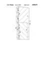
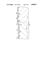
- FIGS. 1 through 4 illustrate a first embodiment of the invention.
- FIGS. 4 through 8 illustrate an alternative embodiment of the invention.
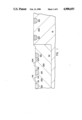
- Area 10 is the substrate (or an epitaxial layer grown above a substrate in the conventional manner) in which the circuit components are to be formed. In this illustration it is N-doped.
- Area 50 is a P-well that is P-doped to provide the complementary N-channel transistors.
- Areas 100 represent an optional step in the process in which areas that will be the field region in the final circuit are doped with a channel topping implant. The field implant will have an effect on the threshold for parasitic transistors.
- the doping agent is boron.
- the doping agent is phosphorous or arsenic. The field implant process is described more fully below with respect to an alternative embodiment of the invention.
- transistors 200 are future active areas in which transistors or other circuit components such as diodes or capacitors will be formed.
- Two such transistors are illustrated, having sources 302 and 312 respectively, drains 304 and 314 respectively, and polysilicon gate electrodes 306 and 316 respectively.
- the problem addressed by the invention is that of a parasitic transistor which can be formed, for example, between drain 314 and source 302 of adjacent transistors if there is a sufficiently high potential above region 100 to form a conducting channel through region 100. If there is some stray charge trapped above region 100, which may occur as a result of ionizing radiation passing through the chip, the charge may also turn on a parasitic transistor.
- the combination of a conductive plate, maintained at an appropriate bias potential, above a thin, high quality oxide serves to suppress the formation of parasitic transistors, in particular to make the circuit more resistant to the formation of parasitic transistors as a result of exposure to ionizing radiation.
- a thin, high quality oxide meaning the same type as a gate oxide
- the structure used here to inhibit transistor formation involves the use of what is effectively a gate oxide normally used to make transistors.
- the N-channel parasitic transistor threshold decreases as the level of radiation exposure increases, so the conductive plate will be maintained at a low or negative potential in order to increase the radiation resistance. The converse is true for N-wells.
- Well 50 is created by a LOCOS process in this embodiment of the invention.
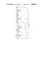
- a thin layer of high quality oxide is grown on the substrate, preferably by a dry process.
- the thickness of this oxide may be between 10 and 100 nm, with a value of 50 nm preferred.
- a thin layer of polysilicon 420 is deposited above oxide layer 410.
- Layer 420 may be between 50 and 200 nm with 150 nm preferred.
- This polysilicon is doped as heavily as possible, illustratively with phosphorous. The doping concentration and the doping process are conventional.
- the active regions 200 are defined with a photo resist and layers 420 and 410 above the active regions are removed.
- the removal step for layer 420 uses an isotropic etch, so that the width of the remaining portion of layer 420 is less than that of layer 410. The reason for this is that in subsequent steps of growing oxide the width of layer 420 will be increased. If it is first reduced in width, then the final edge will not have an overhang (or reentrant angle).
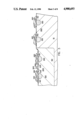
- FIG. 3 there is shown a cross section of the same area in which a layer 430 of oxide has been grown over the active region.
- Differential oxide growth will produce a thicker portion of layer 430 above polysilicon plate 420 than above the single-crystal active area.
- This layer 430 will also be the gate oxide for the transistors that will be placed in the active region, so that it also must be of conventional gate oxide quality.
- the structure of the layers above the field region 100 is: a layer of high quality (gate-type) oxide grown on the substrate by a dry process, a thin layer of doped polycrystalline silicon, and then another layer of grown gate oxide that has been grown into the polycrystalline layer.
- Transistor 300 is shown, for example, having a gate 306 over a thin portion of oxide 430 having the correct conventional gate oxide thickness of 100 nm or so, and source 302 and drain 304 formed in area 200 by a conventional transistor formation process.
- the area of active region 200 has been implanted with a threshold implant to produce the desired transistor threshold, as is conventional in the art.
- the remainder of the circuit is formed according to conventional techniques. Those skilled in the art will readily appreciate that this technique may be applied to NMOS, PMOS, CMOS and various combinations of substrate and well doping (single tub or twin tub), as well as to the use of different doping materials.
- apertures are opened to plates 420, as shown in FIG. 4, and these plates are connected through a metal or polysilicon interconnection layer to a voltage source of predetermined value in order to produce the desired bias on plates 420.
- a layer 440 of oxide has been deposited above insulating layer 430 for insulation and aperture 310 has been opened to permit contact with metal layer 450.
- a second layer of oxide 460 has been deposited above metal 450 and a second layer of metal 470 is above oxide 460, extending down through aperture 308 to make contact with gate 306.
- a corresponding transistor 325 has gate 326 making contact with polysilicon conductor 328, which extends perpendicular to the plane of the paper.
- Conductor 328 is part of a poly layer that will also extend over the field regions, resting on layer 430.
- the transistors will be N-channel and therefore the threshold of the transistors will decrease as the amount of radiation exposure increases.
- the plates 420 in the P-well 50 area should therefore be connected to a low voltage value. Ground may be used if there are only two voltages available. Alternatively, a charge pump or a separate voltage pin on the chip may be used to connect plates 420 to a source of negative voltage.
- the term "potential source terminal" will be used to refer to connection to the "rails", or to the lines connecting to the power supply and also to connection to an on-chip charge pump or other source.
- the field areas in the n-doped epitaxial layer will have p-channel transistors whose threshold increases as a function of radiation exposure and the plates 420 in that region will be connected to a source of relatively positive voltage.
- An advantageous feature of the invention is that the combination of plate 420, oxide 410, and the underlying substrate region 100 forms a capacitor.
- This capacitive layer may be patterned and cut to size to form capacitors of the correct value and used in the circuit.
- a second oxide layer 422 followed by a second polysilicon layer 425 or metal layer 425 may be used to form a second capacitor with 420 as the bottom plate.
- This capacitor may also be used as a circuit element.
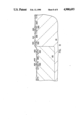
- FIG. 5 there is shown an alternative embodiment of the invention which produces an even greater degree of planarity than the first embodiment.
- similar features of the invention receive the same or similar numbers to the first embodiment.
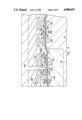
- a substrate 10 with p-well 50 and field regions 100 and active regions 200 is prepared as before.
- the field regions 100 are patterned with a photoresist 115 and then a trench in the range of 200 to 700 nm, preferably 400 nm, is etched into the silicon. These trenches are denoted by the numerals 110.
- An optional phosphorous field implant may be implanted across the wafer, with photoresist 115 still in place, to form the counterparts to areas 100 in the previous embodiment. This implant is intended to control the parasitic transistor threshold in the field regions of the n-doped layer on the right of the figure.
- P-well 50 may be blocked off if that is desired.
- the dose required for setting the n-well threshold in region 10 is smaller than that for the p-well threshold in region 50, so that the presence of this unwanted doping implant in p-well 50 may simply be tolerated.
- a second layer of resist 117 is placed above layer 115 and is patterned with the p-well mask.
- An optional boron field implant heavy enough to compensate for the previous phosphorous, is performed in the p-well field regions that are left open by mask 117. These two implants are those that would be used to form regions 100 in the previous embodiment.
- the resistive layers 115 and 117 are stripped off and a high quality oxide 410 is grown over the entire wafer, as shown in FIG. 6, penetrating into trenches 110 and covering the sides.
- This layer 410 is the same as that in the previous embodiment, with the same option of a sacrificial oxide step.
- a layer 423 of polysilicon is also deposited over the wafer.
- this layer of polysilicon is relatively thick compared to that of the previous embodiment, in the range of 1 to 1.5 microns.
- the polysilicon 423 is deposited thickly enough so that there is essentially no difference in depth over the active regions and field regions.
- a blanket etch of polysilicon 423 is preformed.
- the etchant which may be any of a number of conventional ones that do not attack oxide, is chosen so that the etching process will stop when it reaches oxide layer 410.
- FIG. 7 in which there is a very flat surface layer having the same height as layer 410 and consisting of oxide layer 410 above the active region and a polysilicon plate 423 above the future field region and embedded in oxide.
- An alternative embodiment for this step is to spin on a photo resist and use an etch which attacks the resist at about the same rate as it does the polysilicon. This etchant also must not attack oxide 410. With this alternative, oxide layer 410 may be less thick, since the resist will fill in the depressions above trenches 110 to make a planar starting surface.
- the layer of oxide 410 above the active region is increased and a new layer of oxide 432 above plates 423 in the future field region is grown, preferably by a dry oxidation technique.
- a dry oxidation technique preferably by a dry oxidation technique.
- sacrificial oxidation may be required to make the layer of oxide 432 thick enough to provide isolation from conductors that may pass over the region.
- the transistors, diodes and other circuit elements are then formed by conventional processes, as in the previous embodiment.
- a further advantage is that the vertical displacement of the implanted region in the second embodiment also helps to reduce any unwanted effect on the transistors from the field implant.
- the field plates 420 and 423 in both embodiments can be tied to any convenient voltage value.
- One choice is one of the rail voltages (i.e. p-well plate tied to ground and n-well plate tied to VDD, normally 5 volts). If the circuit is analog, the plates could be tied to the analog voltage while the remainder of the CMOS circuitry is tied to 5 volts and ground. This additional voltage offers a further degree of flexibility to the circuit designer.
- a separate power pin could be added to the circuit to supply power to the field plates. This would permit the application of a negative voltage or a voltage greater than 5 volts.
- An on-chip generated voltage could also be used for plates 420 and 423, with the known engineering trade-off of the use of chip area and the limitations of current supply.
Abstract
Description
Claims (3)
Priority Applications (5)
| Application Number | Priority Date | Filing Date | Title |
|---|---|---|---|
| US07/135,809 US4900693A (en) | 1987-12-21 | 1987-12-21 | Process for making polysilicon field plate with improved suppression of parasitic transistors |
| DE3842749A DE3842749A1 (en) | 1987-12-21 | 1988-12-19 | METHOD FOR PRODUCING AN INTEGRATED CIRCUIT |
| GB8829657A GB2211661B (en) | 1987-12-21 | 1988-12-20 | Semiconductor process with improved suppression of parasitic transistors |
| FR8816924A FR2625037B1 (en) | 1987-12-21 | 1988-12-21 | METHOD FOR MANUFACTURING AN INTEGRATED CIRCUIT BASED ON SILICON |
| JP63323222A JPH022651A (en) | 1987-12-21 | 1988-12-21 | Manufacture of integrated circuit |
Applications Claiming Priority (1)
| Application Number | Priority Date | Filing Date | Title |
|---|---|---|---|
| US07/135,809 US4900693A (en) | 1987-12-21 | 1987-12-21 | Process for making polysilicon field plate with improved suppression of parasitic transistors |
Publications (1)
| Publication Number | Publication Date |
|---|---|
| US4900693A true US4900693A (en) | 1990-02-13 |
Family
ID=22469783
Family Applications (1)
| Application Number | Title | Priority Date | Filing Date |
|---|---|---|---|
| US07/135,809 Expired - Lifetime US4900693A (en) | 1987-12-21 | 1987-12-21 | Process for making polysilicon field plate with improved suppression of parasitic transistors |
Country Status (5)
| Country | Link |
|---|---|
| US (1) | US4900693A (en) |
| JP (1) | JPH022651A (en) |
| DE (1) | DE3842749A1 (en) |
| FR (1) | FR2625037B1 (en) |
| GB (1) | GB2211661B (en) |
Cited By (10)
| Publication number | Priority date | Publication date | Assignee | Title |
|---|---|---|---|---|
| US5111257A (en) * | 1988-12-21 | 1992-05-05 | Mitsubishi Denki Kabushiki Kaisha | Electronic integrated circuit having an electrode layer for element isolation |
| EP0656786A1 (en) | 1992-05-19 | 1995-06-14 | KELLY, Graham Edmund | Health supplements containing phyto-oestrogens, analogues or metabolites thereof |
| US5461248A (en) * | 1991-10-12 | 1995-10-24 | Goldstar Electron Co., Ltd. | Trench capacitor memory cell and process for formation thereof |
| US5521419A (en) * | 1989-02-10 | 1996-05-28 | Mitsubishi Denki Kabushiki Kaisha | Semiconductor device having field shield element isolating structure and method of manufacturing the same |
| US5686754A (en) * | 1994-07-12 | 1997-11-11 | International Rectifier Corporation | Polysilicon field ring structure for power IC |
| US5821600A (en) * | 1994-12-20 | 1998-10-13 | Stmicroelectronics, Inc. | Isolation by active transistors with grounded gates |
| US6091630A (en) * | 1999-09-10 | 2000-07-18 | Stmicroelectronics, Inc. | Radiation hardened semiconductor memory |
| US6380598B1 (en) | 1994-12-20 | 2002-04-30 | Stmicroelectronics, Inc. | Radiation hardened semiconductor memory |
| US20050287754A1 (en) * | 2004-06-25 | 2005-12-29 | Intersil Americas Inc. | Radiation hardened bipolar junction transistor |
| US20060082939A1 (en) * | 2004-09-07 | 2006-04-20 | Summer Steven E | Radiation-tolerant inrush limiter |
Families Citing this family (2)
| Publication number | Priority date | Publication date | Assignee | Title |
|---|---|---|---|---|
| JPH02168666A (en) * | 1988-09-29 | 1990-06-28 | Mitsubishi Electric Corp | Complementary semiconductor device and manufacture thereof |
| JPH0817203B2 (en) * | 1989-08-18 | 1996-02-21 | 三菱電機株式会社 | Semiconductor device and manufacturing method thereof |
Citations (9)
| Publication number | Priority date | Publication date | Assignee | Title |
|---|---|---|---|---|
| US4035829A (en) * | 1975-01-13 | 1977-07-12 | Rca Corporation | Semiconductor device and method of electrically isolating circuit components thereon |
| US4251571A (en) * | 1978-05-02 | 1981-02-17 | International Business Machines Corporation | Method for forming semiconductor structure with improved isolation between two layers of polycrystalline silicon |
| US4270137A (en) * | 1977-12-15 | 1981-05-26 | U.S. Philips Corporation | Field-effect devices |
| US4397077A (en) * | 1981-12-16 | 1983-08-09 | Inmos Corporation | Method of fabricating self-aligned MOS devices and independently formed gate dielectrics and insulating layers |
| US4414560A (en) * | 1980-11-17 | 1983-11-08 | International Rectifier Corporation | Floating guard region and process of manufacture for semiconductor reverse conducting switching device using spaced MOS transistors having a common drain region |
| US4554728A (en) * | 1984-06-27 | 1985-11-26 | International Business Machines Corporation | Simplified planarization process for polysilicon filled trenches |
| US4561170A (en) * | 1984-07-02 | 1985-12-31 | Texas Instruments Incorporated | Method of making field-plate isolated CMOS devices |
| US4685196A (en) * | 1985-07-29 | 1987-08-11 | Industrial Technology Research Institute | Method for making planar FET having gate, source and drain in the same plane |
| US4696092A (en) * | 1984-07-02 | 1987-09-29 | Texas Instruments Incorporated | Method of making field-plate isolated CMOS devices |
Family Cites Families (10)
| Publication number | Priority date | Publication date | Assignee | Title |
|---|---|---|---|---|
| JPS55154743A (en) * | 1979-05-22 | 1980-12-02 | Fujitsu Ltd | Semiconductor device and method of fabricating the same |
| US4290077A (en) * | 1979-05-30 | 1981-09-15 | Xerox Corporation | High voltage MOSFET with inter-device isolation structure |
| JPS5636143A (en) * | 1979-08-31 | 1981-04-09 | Hitachi Ltd | Manufacture of semiconductor device |
| US4470062A (en) * | 1979-08-31 | 1984-09-04 | Hitachi, Ltd. | Semiconductor device having isolation regions |
| JPS59103352A (en) * | 1982-12-06 | 1984-06-14 | Oki Electric Ind Co Ltd | Mos semiconductor integrated circuit device |
| JPS59150465A (en) * | 1983-01-31 | 1984-08-28 | Toshiba Corp | Semiconductor device and manufacture thereof |
| GB2150753B (en) * | 1983-11-30 | 1987-04-01 | Toshiba Kk | Semiconductor device |
| JPS60206040A (en) * | 1984-03-30 | 1985-10-17 | Hitachi Ltd | Insulation isolator for semiconductor ic |
| US4612563A (en) * | 1984-07-30 | 1986-09-16 | Sprague Electric Company | High voltage integrated circuit |
| JPS62162353A (en) * | 1986-01-13 | 1987-07-18 | Oki Electric Ind Co Ltd | Manufacture of mos semiconductor device |
-
1987
- 1987-12-21 US US07/135,809 patent/US4900693A/en not_active Expired - Lifetime
-
1988
- 1988-12-19 DE DE3842749A patent/DE3842749A1/en not_active Ceased
- 1988-12-20 GB GB8829657A patent/GB2211661B/en not_active Expired - Fee Related
- 1988-12-21 FR FR8816924A patent/FR2625037B1/en not_active Expired - Fee Related
- 1988-12-21 JP JP63323222A patent/JPH022651A/en active Pending
Patent Citations (9)
| Publication number | Priority date | Publication date | Assignee | Title |
|---|---|---|---|---|
| US4035829A (en) * | 1975-01-13 | 1977-07-12 | Rca Corporation | Semiconductor device and method of electrically isolating circuit components thereon |
| US4270137A (en) * | 1977-12-15 | 1981-05-26 | U.S. Philips Corporation | Field-effect devices |
| US4251571A (en) * | 1978-05-02 | 1981-02-17 | International Business Machines Corporation | Method for forming semiconductor structure with improved isolation between two layers of polycrystalline silicon |
| US4414560A (en) * | 1980-11-17 | 1983-11-08 | International Rectifier Corporation | Floating guard region and process of manufacture for semiconductor reverse conducting switching device using spaced MOS transistors having a common drain region |
| US4397077A (en) * | 1981-12-16 | 1983-08-09 | Inmos Corporation | Method of fabricating self-aligned MOS devices and independently formed gate dielectrics and insulating layers |
| US4554728A (en) * | 1984-06-27 | 1985-11-26 | International Business Machines Corporation | Simplified planarization process for polysilicon filled trenches |
| US4561170A (en) * | 1984-07-02 | 1985-12-31 | Texas Instruments Incorporated | Method of making field-plate isolated CMOS devices |
| US4696092A (en) * | 1984-07-02 | 1987-09-29 | Texas Instruments Incorporated | Method of making field-plate isolated CMOS devices |
| US4685196A (en) * | 1985-07-29 | 1987-08-11 | Industrial Technology Research Institute | Method for making planar FET having gate, source and drain in the same plane |
Non-Patent Citations (4)
| Title |
|---|
| Ghandhi, S. K., VLSI Fabrication Principles, John Wiley & Sons, 1983, pp. 376 401. * |
| Ghandhi, S. K., VLSI Fabrication Principles, John Wiley & Sons, 1983, pp. 376-401. |
| Sze, S. M., VLSI Technology, McGraw Hill, 1983, pp. 140 157. * |
| Sze, S. M., VLSI Technology, McGraw-Hill, 1983, pp. 140-157. |
Cited By (17)
| Publication number | Priority date | Publication date | Assignee | Title |
|---|---|---|---|---|
| US5111257A (en) * | 1988-12-21 | 1992-05-05 | Mitsubishi Denki Kabushiki Kaisha | Electronic integrated circuit having an electrode layer for element isolation |
| US5521419A (en) * | 1989-02-10 | 1996-05-28 | Mitsubishi Denki Kabushiki Kaisha | Semiconductor device having field shield element isolating structure and method of manufacturing the same |
| US5461248A (en) * | 1991-10-12 | 1995-10-24 | Goldstar Electron Co., Ltd. | Trench capacitor memory cell and process for formation thereof |
| EP0656786A1 (en) | 1992-05-19 | 1995-06-14 | KELLY, Graham Edmund | Health supplements containing phyto-oestrogens, analogues or metabolites thereof |
| US5686754A (en) * | 1994-07-12 | 1997-11-11 | International Rectifier Corporation | Polysilicon field ring structure for power IC |
| US6380598B1 (en) | 1994-12-20 | 2002-04-30 | Stmicroelectronics, Inc. | Radiation hardened semiconductor memory |
| US5821600A (en) * | 1994-12-20 | 1998-10-13 | Stmicroelectronics, Inc. | Isolation by active transistors with grounded gates |
| US5849614A (en) * | 1994-12-20 | 1998-12-15 | Sgs Thomson Microelectronics, Inc. | Method of isolation by active transistors with grounded gates |
| US6656803B2 (en) | 1994-12-20 | 2003-12-02 | Stmicrocelectronics, Inc. | Radiation hardened semiconductor memory |
| US6194276B1 (en) * | 1999-09-10 | 2001-02-27 | Stmicroelectronics, Inc. | Radiation hardened semiconductor memory |
| US6091630A (en) * | 1999-09-10 | 2000-07-18 | Stmicroelectronics, Inc. | Radiation hardened semiconductor memory |
| US20050287754A1 (en) * | 2004-06-25 | 2005-12-29 | Intersil Americas Inc. | Radiation hardened bipolar junction transistor |
| US7029981B2 (en) * | 2004-06-25 | 2006-04-18 | Intersil Americas, Inc. | Radiation hardened bipolar junction transistor |
| US20060157736A1 (en) * | 2004-06-25 | 2006-07-20 | Vonno Nicolaas W V | Radiation hardened bipolar junction transistor |
| US7187056B2 (en) * | 2004-06-25 | 2007-03-06 | Intersil Americas, Inc. | Radiation hardened bipolar junction transistor |
| US20060082939A1 (en) * | 2004-09-07 | 2006-04-20 | Summer Steven E | Radiation-tolerant inrush limiter |
| US8072726B2 (en) * | 2004-09-07 | 2011-12-06 | Summer Steven E | Radiation-tolerant inrush limiter |
Also Published As
| Publication number | Publication date |
|---|---|
| FR2625037A1 (en) | 1989-06-23 |
| GB2211661A (en) | 1989-07-05 |
| GB8829657D0 (en) | 1989-02-15 |
| DE3842749A1 (en) | 1989-07-06 |
| GB2211661B (en) | 1991-05-08 |
| JPH022651A (en) | 1990-01-08 |
| FR2625037B1 (en) | 1994-04-01 |
Similar Documents
| Publication | Publication Date | Title |
|---|---|---|
| US5376578A (en) | Method of fabricating a semiconductor device with raised diffusions and isolation | |
| JP3431734B2 (en) | SOI field effect transistor and method of manufacturing the same | |
| US5128274A (en) | Method for producing a semiconductor device having a LOCOS insulating film with at least two different thickness | |
| EP0334761B1 (en) | Method for forming a self-aligned source/drain contact for a MOS transistor | |
| US5145802A (en) | Method of making SOI circuit with buried connectors | |
| US6548859B2 (en) | MOS semiconductor device and method of manufacturing the same | |
| KR100204078B1 (en) | Soi dram having field separate area | |
| US5293053A (en) | Elevated CMOS | |
| US7053465B2 (en) | Semiconductor varactor with reduced parasitic resistance | |
| US4980306A (en) | Method of making a CMOS device with trench isolation device | |
| US6228726B1 (en) | Method to suppress CMOS device latchup and improve interwell isolation | |
| EP0749165A2 (en) | Thin film transistor in insulated semiconductor substrate and manufacturing method thereof | |
| US7256439B2 (en) | Trench capacitor array having well contacting merged plate | |
| US5573969A (en) | Method for fabrication of CMOS devices having minimized drain contact area | |
| KR100543564B1 (en) | Semiconductor device and its production method | |
| US5369049A (en) | DRAM cell having raised source, drain and isolation | |
| JP2002324905A (en) | Method of forming integrated circuit having body contact | |
| JP4121356B2 (en) | Semiconductor device | |
| US6294817B1 (en) | Source/drain-on insulator (S/DOI) field effect transistor using oxidized amorphous silicon and method of fabrication | |
| JPH11274496A (en) | Field-effect transistor having improved implant and its manufacture | |
| KR20070072928A (en) | Semiconductor device and its manufacturing method | |
| US5457339A (en) | Semiconductor device for element isolation and manufacturing method thereof | |
| US5726476A (en) | Semiconductor device having a particular CMOS structure | |
| US4900693A (en) | Process for making polysilicon field plate with improved suppression of parasitic transistors | |
| US20040146701A1 (en) | Semiconductor substrate having SOI structure and manufacturing method and semiconductor device thereof |
Legal Events
| Date | Code | Title | Description |
|---|---|---|---|
| AS | Assignment |
Owner name: UNITED TECHNOLOGIES CORPORATION, HARTFORD, CONNECT Free format text: ASSIGNMENT OF ASSIGNORS INTEREST.;ASSIGNOR:MANNING, ROBERT W.;REEL/FRAME:004805/0930 Effective date: 19871208 Owner name: UNITED TECHNOLOGIES CORPORATION, HARTFORD, CONNECT Free format text: ASSIGNMENT OF ASSIGNORS INTEREST;ASSIGNOR:MANNING, ROBERT W.;REEL/FRAME:004805/0930 Effective date: 19871208 |
|
| STCF | Information on status: patent grant |
Free format text: PATENTED CASE |
|
| FEPP | Fee payment procedure |
Free format text: PAYOR NUMBER ASSIGNED (ORIGINAL EVENT CODE: ASPN); ENTITY STATUS OF PATENT OWNER: LARGE ENTITY |
|
| FPAY | Fee payment |
Year of fee payment: 4 |
|
| FPAY | Fee payment |
Year of fee payment: 8 |
|
| AS | Assignment |
Owner name: UTMC MICROELECTRONIC SYSTEMS INC., COLORADO Free format text: ASSIGNMENT OF ASSIGNORS INTEREST;ASSIGNOR:UNITED TECHNOLOGIES CORPORATION, A DELAWARE CORPORATION;REEL/FRAME:009893/0312 Effective date: 19990225 |
|
| FPAY | Fee payment |
Year of fee payment: 12 |