US4934852A - Variable color display typewriter - Google Patents
Variable color display typewriter Download PDFInfo
- Publication number
- US4934852A US4934852A US07/336,080 US33608089A US4934852A US 4934852 A US4934852 A US 4934852A US 33608089 A US33608089 A US 33608089A US 4934852 A US4934852 A US 4934852A
- Authority
- US
- United States
- Prior art keywords
- color
- typing
- memory
- display
- green
- Prior art date
- Legal status (The legal status is an assumption and is not a legal conclusion. Google has not performed a legal analysis and makes no representation as to the accuracy of the status listed.)
- Expired - Fee Related
Links
Images


Classifications
-
- B—PERFORMING OPERATIONS; TRANSPORTING
- B41—PRINTING; LINING MACHINES; TYPEWRITERS; STAMPS
- B41J—TYPEWRITERS; SELECTIVE PRINTING MECHANISMS, i.e. MECHANISMS PRINTING OTHERWISE THAN FROM A FORME; CORRECTION OF TYPOGRAPHICAL ERRORS
- B41J3/00—Typewriters or selective printing or marking mechanisms characterised by the purpose for which they are constructed
- B41J3/44—Typewriters or selective printing mechanisms having dual functions or combined with, or coupled to, apparatus performing other functions
- B41J3/46—Printing mechanisms combined with apparatus providing a visual indication
-
- G—PHYSICS
- G09—EDUCATION; CRYPTOGRAPHY; DISPLAY; ADVERTISING; SEALS
- G09F—DISPLAYING; ADVERTISING; SIGNS; LABELS OR NAME-PLATES; SEALS
- G09F9/00—Indicating arrangements for variable information in which the information is built-up on a support by selection or combination of individual elements
- G09F9/30—Indicating arrangements for variable information in which the information is built-up on a support by selection or combination of individual elements in which the desired character or characters are formed by combining individual elements
- G09F9/33—Indicating arrangements for variable information in which the information is built-up on a support by selection or combination of individual elements in which the desired character or characters are formed by combining individual elements being semiconductor devices, e.g. diodes
Definitions
- This invention relates to typewriters utilizing variable color display.
- a display device that can change color and selectively display characters described in my U.S. Pat. No. 4,086,514, issued on Apr. 25, 1978 and entitled Variable Color Display Device, includes display areas with three light emitting diodes for emitting variable portions of light signals of respectively different primary colors, which are blended within each display area to form a composite light signal.
- Monochromatic display typewriters have flourished in recent years and are extensively used. Such display typewriters, however, are capable of visually presenting only the typed text. They are not capable of simultaneously indicating the typing speed and accuracy.
- An electronic typewriter disclosed in U.S. Pat. No. 4,323,315, issued on Apr. 6, 1982 to Filippo Demonte et al. and entitled Electronic Typewriter with Display Device includes a monochromatic display which is capable of displaying characters with different kinds of emphasis.
- a microprocessor-based display controller for 5 ⁇ 7 matrix monochromatic display is described in Hewlett-Packard application note 1001, pages 398-413, issued in 1980 and entitled Interfacing the HDSP-2000 to Microprocessor Systems.
- a device for indicating typing speed and rhythm disclosed in U.S. Pat. No. 2,717,688, issued on Sept. 13, 1955 to James A. Brooks and entitled Typing Speed and Rhythm Indicating Apparatus for Typewriters includes a light bulb which remains continuously lit when the typist keeps depressing keys with sufficient speed and uniformity.
- An electronic typewriter described in West German Patent No. 3,534,569, issued on Apr. 3, 1986 to O. Flugel et al. and entitled Electronic Typewriter with Print Speed Monitoring, includes a monochromatic display for digitally indicating typing speed.
- a word processing system disclosed in U.S. Pat. No. 4,136,395, issued on Jan. 23, 1979 to Robert A. Kolpek et al. and entitled System for Automatically Proofreading a Document includes a dictionary memory and comparator for detecting spelling errors.
- the invention endeavors to overcome problems of the prior art display typewriters by providing a new type of a display typewriter.
- variable color display typewriter that visually presents typed text in a color variable in accordance with the typing speed.
- Such typewriter is ideally suited for professional typists and for those who strive to improve and polish their typing skills.
- FIG. 1 is a block diagram of 2-primary color display system.
- FIG. 2 is a block diagram of 3-primary color display system.
- FIG. 3 is an enlarged detail of one digit of 2-primary color digital display.
- FIG. 4 is an enlarged cross-sectional view of one display segment in FIG. 3, taken along the line 4--4.
- FIG. 5 is an enlarged detail of one digit of 3-primary color digital display.
- FIG. 6 is an enlarged cross-sectional view of one display segment in FIG. 5, taken along the line 6--6.
- FIG. 7 is a schematic diagram of one 2-primary color display element.
- FIG. 8 is a schematic diagram of one 3-primary color display element.
- FIG. 9 is a simplified schematic diagram, similar to FIG. 7, showing how number ⁇ 7 ⁇ can be displayed in three different colors.
- FIG. 10 is a simplified schematic diagram, similar to FIG. 8, showing how number ⁇ 1 ⁇ can be displayed in seven different colors.
- FIG. 11 is a block diagram of 2-primary color 4-digit display.
- FIG. 12 is a block diagram of 3-primary color 4-digit display.
- FIG. 13 is an expanded block diagram of 2-LED color converter.
- FIG. 14 is an expanded block diagram of 3-LED color converter.
- FIG. 15 is a schematic diagram of a scaling circuit.
- FIG. 16 is a schematic diagram of an A/D converter and memory combination of FIGS. 13 and 14.
- FIG. 17 is a schematic diagram of a memory and color converter combination of FIG. 13.
- FIG. 18 is a timing diagram of the circuit shown in FIG. 17.
- FIG. 19 is a schematic diagram of a memory and color converter combination of FIG. 14.
- FIG. 20 is a timing diagram of the circuit shown in FIG. 19.
- FIG. 21 is a continuation of the timing diagram of FIG. 20.
- FIG. 22 is a graphic representation of TABLE 1.
- FIG. 23 is a graphic representation of TABLE 2.
- FIG. 24 is a graph of the ICI chromaticity diagram.
- FIG. 25 is a general block diagram of a variable color display typewriter wherein the color of the display is variable in accordance with the typing speed.
- FIG. 26 is a general block diagram of a variable color display typewriter wherein the color of the display is variable in accordance with the typing accuracy.
- FIG. 27 is an expanded block diagram of a variable color display typewriter shown in FIG. 25.
- FIG. 28 is an expanded block diagram of a variable color display typewriter shown in FIG. 26.
- FIG. 29 is an expanded diagram of a typing speed converter for controlling the color of the typewriter display in steps.
- FIG. 30 is an expanded diagram of a like typing speed converter for controlling the color of the typewriter display continuously.
- FIG. 31 is a timing diagram showing the relationship between the measured typing speed and generated COUNTER SAVE and COUNTER CLEAR signals.
- FIG. 32 is a detail of the combination of the counter shown generally in FIG. 30 with a memory for 2-primary color converter.
- FIG. 33 is a detail of the combination of the counter shown generally in FIG. 30 with a memory for 3-primary color converter.
- FIG. 34 is a schematic diagram of a circuit for generating COUNTER SAVE and COUNTER CLEAR signals.
- FIG. 35 is a schematic diagram of an oscillator shown generally in FIGS. 29 and 30.
- FIG. 36 is a detail of the counter and decoder combination shown generally in FIG. 29 for controlling the color of the typewriter display in three steps.
- FIG. 37 is a detail of the counter and decoder combination shown generally in FIG. 29 for controlling the color of the typewriter display in seven steps.
- FIG. 38 is a block diagram of a variable color display typewriter controlled by a central processor.
- FIG. 39 is a detail of the color memory of FIG. 38 for controlling the color of the typewriter display in three steps.
- FIG. 40 is a like detail of the color memory of FIG. 38 for controlling the color of the typewriter display in seven steps.
- FIG. 41 is a detail of the color memory of FIG. 38 used in a 2-LED continuously variable color converter.
- FIG. 42 is a detail of the color memory of FIG. 38 used in a 3-LED continuously variable color converter.
- FIG. 43 is a block diagram of a CPU controlled variable color display typewriter with spelling checker.
- FIG. 44 is a top view of a variable color display typewriter of the present invention.
- FIG. 45 is a detail of a variable color typewriter display showing the interconnection of three step variable color display elements.
- FIG. 46 is a detail of a variable color typewriter display showing the interconnection of seven step variable color display elements.
- FIG. 47 is a detail of a variable color typewriter display showing the interconnection of continuously variable color 2-LED display elements.
- FIG. 48 is a detail of a variable color typewriter display showing the interconnection of continuously variable color 3-LED display elements.
- TABLE 1 shows the characteristic of a step variable 2-primary color converter.
- TABLE 2 shows a rainbow-like characteristic of a continuously variable 3-primary color converter.
- CHART 1 shows the relationship between count retained in the counter of FIG. 36, typing speed limits, and resulting color of the typewriter display.
- CHART 2 shows the relationship between count retained in the counter of FIG. 37, typing speed limits, and resulting color of the typewriter display.
- CHART 3 shows the relationship between time limits for typing 10 characters, binary code stored in the color memory of FIG. 39, typing speed limits, and resulting color of the typewriter display.
- CHART 4 shows the relationship between time limits for typing 10 characters, binary code stored in the color memory of FIG. 40, typing speed limits, and resulting color of the typewriter display.
- FIG. 1 a block diagram of a 2-primary color display system including a display decoder 21, a variable color 2-LED display element 46, and a 2-primary color control 52.
- the display decoder 21 accepts at its inputs a code representing the character to be displayed and accordingly develops output drive signals to drive respective segments of display element 46.
- the color control 52 accepts color control signals at its inputs R (red), Y (yellow), and G (green) and develops at its outputs drive signals for red bus 5 and green bus 6, respectively, to illuminate display element 46 in a selected color.
- FIG. 2 is shown a block diagram of a 3-primary color display system including a display decoder 21, a variable color 3-LED display element 47, and a 3-primary color control 53.
- the color control 53 accepts color control signals at its inputs R (red), Y (yellow), G (green), BG (blue-green), B (blue), P (purple), and W (white) and develops at its outputs drive signals for red bus 5, green bus 6, and blue bus 7, respectively, to illuminate display element 47 in a selected color.
- the 2-primary color display element 46 includes seven elongated display segments a, b, c, d, e, f, and g, arranged in a conventional pattern, which may be selectively energized in different combinations to display the desired digits.
- Each display segment includes a pair of LEDs (light emitting diodes): red LED 2 and green LED 3, which are closely adjacent such that the light signals emitted therefrom are substantially superimposed upon each other to mix the colors.
- the LEDs are designated by segment symbols, e.g., the red LED in the segment a is designated as 2a, etc.
- red LED 2e and green LED 3e are placed on the base of a segment body 15a which is filled with a transparent light scattering material 16.
- LEDs 2e and 3e emit light signals of red and green colors, respectively, which are scattered within transparent material 16, thereby blending the red and green light signals into a composite light signal that emerges at the upper surface of segment body 15a.
- the color of the composite light signal may be controlled by varying the portions of the red and green light signals.
- each display segment of the 3-primary color display element 47 includes a triad of LEDs: red LED 2, green LED 3, and blue LED 4, which are closely adjacent such that the light signals emitted therefrom are substantially superimposed upon one another to mix the colors.
- red LED 2e, green LED 3e, and blue LED 4e are placed on the base of a segment body 15b which is filled with a transparent light scattering material 16.
- Red LEDs are typically manufactured by diffusing a p-n junction into a GaAsP epitaxial layer on a GaAs substrate; green LEDs typically use a GaP epitaxial layer on a GaP substrate; blue LEDs are typically made from SiC material.
- LEDs 2e, 3e, and 4e When forwardly biased, LEDs 2e, 3e, and 4e emit light signals of red, green, and blue colors, respectively, which are scattered within transparent material 16, thereby blending the red, green, and blue light signals into a composite light signal that emerges at the upper surface of segment body 15b.
- the color of the composite light signal may be controlled by varying the portions of the red, green, and blue light signals.
- FIG. 7 is shown a schematic diagram of a 2-primary color common cathodes 7-segment display element 42 which can selectively display various digital fonts in different colors on display segments a, b, c, d, e, f, g, and DP (Decimal Point).
- the anodes of all red and green LED pairs are interconnected in each display segment and are electrically connected to respective outputs of a commercially well known common-cathode 7-segment decoder driver 23.
- the cathodes of all red LEDs 2a, 2b, 2c, 2d, 2e, 2f, 2g, and 2i are interconnected to a common electric path referred to as a red bus 5.
- the cathodes of all green LEDs 3a, 3b, 3c, 3d, 3e, 3f, 3g, and 3i are interconnected to a like common electric path referred to as a green bus 6.
- the red bus 5 is connected to the output of a tri-state inverting buffer 63a, capable of sinking sufficient current to forwardly bias all red LEDs 2a to 2i in display element 42.
- the green bus 6 is connected to the output of a like buffer 63b.
- the two buffers 63a and 63b can be simultaneously enabled by applying a low logic level signal to the input of inverter 64a, and disabled by applying a high logic level signal thereto.
- the conditions of red bus 5 and green bus 6 can be selectively controlled by applying suitable logic control signals to the bus control inputs RB (red bus) and GB (green bus), to illuminate display element 42 in a selected color.
- buffers 63a and 63b are disabled, both red bus 5 and green bus 6 are effectively disconnected to cause display element 42 to be completely extinguished.
- FIG. 8 is shown a schematic diagram of a 3-primary color common anodes 7-segment display element 43 which can selectively display digital fonts in different colors.
- the cathodes of all red, green, and blue LED triads in each display segment are interconnected and electrically connected to respective outputs of a commercially well know common anode 7-segment decoder driver 24.
- the anodes of all red LEDs 2a, 2b, 2c, 2d, 2e, 2f, and 2g are interconnected to form a common electric path referred to as a red bus 5.
- the anodes of all green LEDs 3a, 3b, 3c, 3d, 3e, 3f, and 3g are interconnected to form a like common electric path referred to as a green bus 6.
- the anodes of all blue LEDs 4a, 4b, 4c, 4d, 4e, 4f, and 4g are interconnected to form a like common electric path referred to as a blue bus 7.
- the red bus 5 is connected to the output of a non-inverting tri-state buffer 62a, capable of sourcing sufficient current to illuminate all red LEDs 2a to 2g in display element 43.
- the green bus 6 is connected to the output of a like buffer 62b.
- the blue bus 7 is connected to the output of a like buffer 62c.
- the three buffers 62a, 62b, and 62c can be simultaneously enabled, by applying a low logic level signal to the input of inverter 64b, and disabled by applying a high logic level signal thereto.
- red bus 5, green bus 6, and blue bus 7 can be selectively controlled by applying valid combinations of logic level signals to the bus control inputs RB (red bus), GB (green bus), and BB (blue bus), to illuminate display element 43 in a selected color.
- red bus 5, green bus 6, and blue bus 7 are effectively disconnected to cause display element 43 to be completely extinguished.
- FIG. 9 A simplified schematic diagram to facilitate the explanation is shown in FIG. 9. Any digit between 0 and 9 can be selectively displayed by applying the appropriate BCD code to the inputs A0, A1, A2, and A3 of common-cathode 7-segment decoder driver 23.
- the decoder driver 23 develops at its outputs a, b, c, d, e, f, g, and DP drive signals for energizing selected groups of the segments to thereby visually display the selected number, in a manner well known to those having ordinary skill in the art.
- a BCD code 0111 is applied to the inputs A0, A1, A2, and A3.
- the decoder driver 23 develops high voltage levels at its outputs a, b, and c, to illuminate equally designated segments a, b, and c, and low voltage levels at all remaining outputs (not shown), to extinguish all remaining segments d, e, f, and g.
- the color control input R is raised to a high logic level, and the color control inputs Y and G are maintained at a low logic level.
- the output of OR gate 60a rises to a high logic level, thereby causing the output of buffer 63a to drop to a low logic level.
- the current flows from the output a of decoder driver 23, via red LED 2a and red bus 5, to current sinking output of buffer 63a.
- the current flows from the output b of decoder driver 23, via red LED 2b and red bus 5, to the output of buffer 63a.
- the current flows from the output c of decoder driver 23, via red LED 2c and red bus 5, to the output of buffer 63a.
- segments a, b, and c illuminate in red color, thereby causing a visual impression of a character ⁇ 7 ⁇ .
- the green LEDs 3a, 3b, 3c remain extinguished because the output of buffer 63b is at a high logic level, thereby disabling green bus 6.
- the color control input G is raised to a high logic level, while the color control inputs R and Y are maintained at a low logic level.
- the output of OR gate 60b rises to a high logic level, thereby causing the output of buffer 63b to drop to a low logic level.
- the current flows from the output a of decoder driver 23, via green LED 3a and green bus 6, to current sinking output of buffer 63b.
- the current flows from the output b of decoder driver 23, via green LED 3b and green bus 6, to the output of buffer 63b.
- the current flows from the output c of decoder driver 23, via green LED 3c and green bus 6, to the output of buffer 63b.
- segments a, b, and c illuminate in green color.
- the red LEDs 2a, 2b, and 2c remain extinguished because the output of buffer 63a is at a high logic level, thereby disabling red bus 5.
- the color control input Y is raised to a high logic level, while the color inputs R and G are maintained at a low logic level.
- the outputs of both OR gates 60a and 60b rise to a high logic level, thereby causing the outputs of both buffers 63a and 63b to drop to a low logic level.
- the current flows from the output a of decoder driver 23, via red LED 2a and red bus 5, to current sinking output of buffer 63a, and, via green LED 3a and green bus 6, to current sinking output of buffer 63b.
- the current flows from the output b of decoder driver 23, via red LED 2b and red bus 5, to the output of buffer 63a, and, via green LED 3b and green bus 6, to the output of buffer 63b.
- the current flows from the output c of decoder driver 23, via red LED 2c and red bus 5, to the output of buffer 63a, and, via green LED 3c and green bus 6, to the output of buffer 63b.
- FIG. 10 A simplified schematic diagram to facilitate the explanation is shown in FIG. 10.
- a BCD code 0001 is applied to the inputs A0, A1, A2, and A3 of common anode 7-segment decoder driver 24.
- the decoder driver 24 develops low voltage levels at its outputs b and c, to illuminate equally designated segments b and c, and high voltage levels at all remaining outputs (not shown), to extinguish all remaining segments a, d, e, f, and g.
- the color control input R is raised to a high logic level, while all remaining color control inputs are maintained at a low logic level.
- the output of OR gate 61a rises to a high logic level, thereby causing the output of buffer 62a to rise to a high logic level.
- the current flows from the output of buffer 62a, via red bus 5 and red LED 2b, to the output b of decoder driver 24, and, via red LED 2c, to the output c of decoder driver 24.
- segments b and c illuminate in red color, thereby causing a visual impression of a character ⁇ 1 ⁇ .
- the green LEDs 3b, 3c and blue LEDs 4b, 4c remain extinguished because green bus 6 and blue bus 7 are disabled.
- the color control input G is raised to a high logic level, while all remaining color control inputs are maintained at a low logic level.
- the output of OR gate 61b rises to a high logic level, thereby causing the output of buffer 62b to rise to a high logic level.
- the current flows from the output of buffer 62b, via green bus 6 and green LED 3b, to the output b of decoder driver 24, and, via green LED 3c, to the output c of decoder driver 24.
- segments b and c illuminate in green color.
- the color control input B is raised to a high logic level, while all remaining color control inputs are maintained at a low logic level.
- the output of OR gate 61c rises to a high logic level, thereby causing the output of buffer 62c to rise to a high logic level.
- the current flows from the output of buffer 62c, via blue bus 7 and blue LED 4b, to the output b of decoder driver 24, and, via blue LED 4c, to the output c of decoder driver 24.
- segments b and c illuminate in blue color.
- the color control input Y is raised to a high logic level, while all remaining color control inputs are maintained at a low logic level.
- the outputs of OR gates 61a and 61b rise to a high logic level, thereby causing the outputs of buffers 62a and 62b to rise to a high logic level.
- the current flows from the output of buffer 62a, via red bus 5 and red LED 2b, to the output b of decoder driver 24, and, via red LED 2c, to the output c of decoder driver 24.
- the current also flows from the output of buffer 62b, via green bus 6 and green LED 3b, to the output b of decoder driver 24, and, via green LED 3c, to the output c of decoder driver 24.
- the segments b and c illuminate in substantially yellow color.
- the color control input P is raised to a high logic level, while all remaining color control inputs are maintained at a low logic level.
- the outputs of OR gates 61a and 61c rise to a high logic level, thereby causing the outputs of buffers 62a and 62c to rise to a high logic level.
- the current flows from the output of buffer 62a, via red bus 5 and red LED 2b, to the output b of decoder driver 24, and, via red LED 2c, to the output c of decoder driver 24.
- the current also flows from the output of buffer 62c, via blue bus 7 and blue LED 4b, to the output b of decoder driver 24, and, via blue LED 4c, to the output c of decoder driver 24.
- segments b and c illuminate in substantially purple color.
- the color control input BG is raised to a high logic level, while all remaining color control inputs are maintained at a low logic level.
- the outputs of OR gates 61b and 61c rise to a high logic level, thereby causing the outputs of buffers 62b and 62c to rise to a high logic level.
- the current flows from the output of buffer 62b, via green bus 6 and green LED 3b, to the output b of decoder driver 24, and, via green LED 3c, to the output c of decoder driver 24.
- the current also flows from the output of buffer 62c, via blue bus 7 and blue LED 4b, to the output b of decoder driver 24, and, via blue LED 4c, to the output c of decoder driver 24.
- segments b and c illuminate in substantially blue-green color.
- the color control input W is raised to a high logic level, while all remaining color control inputs are maintained at a low logic level.
- the outputs of OR gates 61a, 61b, and 61c rise to a high logic level, thereby causing the outputs of respective buffers 62a, 62b, and 62c to rise to a high logic level.
- the current flows from the output of buffer 62a, via red bus 5 and red LED 2b, to the output b of decoder driver 24, and, via red LED 2c, to the output c of decoder driver 24.
- the current also flows from the output of buffer 62b, via green bus 6 and green LED 3b, to the output b of decoder driver 24, and, via green LED 3c, to the output c of decoder driver 24.
- the current also flows from the output of buffer 62c, via blue bus 7 and blue LED 4b, to the output b of decoder driver 24, and, via blue LED 4c, to the output c of decoder driver 24.
- decoder driver 24 may be overloaded by driving a triad of LEDs in parallel in display element 43, rather than a single LED in a monochromatic display, it would be obvious to employ suitable buffers to drive respective color display segments (not shown).
- FIG. 11 To illustrate how the present invention can be utilized in a multi-element variable color display configuration, in FIG. 11 is shown a detail of the interconnection in a 2-primary color 4-digit display having display segments 1a, 1b, 1c, and 1d arranged in a 7-segment font.
- the color control inputs R, Y, and G of color controls 52a, 52b, 52c, and 52d of all display elements 46a, 46b, 46c, and 46d are interconnected, respectively, and enable inputs E1, E2, E3, and E4 are used to control the conditions of respective display elements 46a, 46b, 46c, and 46d.
- a high logic level at the enable input E extinguishes the particular display element 46a, 46b, 46c, or 46d; a low logic level therein illuminates display element 46a, 46b, 46c, or 46d in a color determined by the instant conditions of the color control inputs R, Y, and G.
- FIG. 12 is shown a like detail of the interconnection in a 3-primary color 4-digit display having display segments 1a, 1b, 1c, and 1d arranged in a 7-segment font.
- the color control inputs B, P, BG, G, Y, W, and R of color controls 53a, 53b, 53c, and 53d of all display elements 47a, 47b, 47c, and 47d are interconnected, and the conditions of respective display elements 47a, 47b, 47c, and 47d are controlled by enable inputs E1, E2, E3, and E4.
- a high logic level at the enable input E extinguishes the particular display element 47a, 47b, 47c, or 47d; a low logic level therein illuminates display element 47a, 47b, 47c, or 47d in a color determined by the instant conditions of the color control inputs B, P, BG, G, Y, W, and R.
- the exemplary color control circuits described herein will cooperate equally well with a multi-element variable color display constructed either in common cathodes or in common anodes configuration.
- the display system shown in FIG. 13 utilizes a scaling circuit 80a which scales input analog voltage levels to a voltage range suitable for an A/D converter 74a, which in turn develops at its outputs a digital code having relation to the value of the input analog voltage.
- the output lines of A/D converter 74a are connected to the address inputs of a memory 76 having a plurality of addressable locations which contain data indicating the portions of red color for several different values of the input analog voltage.
- the output data of memory 76 are applied to the inputs of a color converter 57 which will develop control signals for red bus 5 and green bus 6, respectively, of variable color display element 42.
- the display system shown in FIG. 14 utilizes a scaling circuit 80b and an A/D converter 74b for converting the instant value of an input analog voltage to a digital code.
- the outputs of A/D converter 74b are connected, in parallel, to the address inputs of memory 76a, which contains data indicating the portions of red color, to the address inputs of memory 76b, which contains data indicating the portions of green color, and to the address inputs of memory 76c, which contains data indicating the portions of blue color.
- the output data of memory 76a are applied to red color converter 59a which will develop control signals for red bus 5 of variable color display element 43.
- the output data of memory 76b are applied to green color converter 59b which will develop control signals for green bus 6 of display element 43.
- the output data of memory 76c are applied to blue color converter 59c which will develop control signals for blue bus 7 of display element 43.
- FIG. 15 is a schematic diagram of a scaling circuit capable of shifting and amplifying the input voltage levels.
- the circuit utilizes two operational amplifiers 81a and 81b in a standard inverting configuration.
- the amplifier 81a is set for a unity gain by using resistors 90a and 90b of equal values; potentiometer 92a is adjusted to set a desired offset voltage.
- the amplifier 81b sets the gain by adjusting feedback potentiometer 92b to a desired value with respect to resistor 90c.
- an input voltage which may vary between arbitrary limits Vlow and Vhigh, may be scaled and shifted to the range between 0 Volts and 9.961 Volts, to facilitate the use of a commercially available A/D converter.
- FIG. 16 is a schematic diagram of an A/D (analog-to-digital) converter 75 which is capable of converting input analog voltage, applied via resistor 90e to its input Vin, to 8-bit digital data for addressing a memory 77.
- the conversion may be initiated from time to time by applying a short positive pulse 99a to the Blank and Convert input B&C.
- A/D converter 75 will thereafter perform a conversion of the instant input voltage to 8-bit data indicative of its value.
- the Data Ready output drops to a low logic level, thereby indicating that the data are available at the outputs Bit 1 to Bit 8, which are directly connected to respective address inputs A0 to A7 of memory 77.
- the Chip Select input CS of memory 77 is activated, memory 77 is enabled, and the data, residing at the address selected by the instant output of A/D converter 75, will appear at its data outputs D0 to D7.
- a clock signal 99b of a suitable frequency (e.g., 10 kHz), to provide a flicker-free display, is applied to the Clock Pulse inputs CP of 8-bit binary counters 71e and 71f to step them down.
- the Terminal Count output TC of counter 71e drops to a low logic level for one clock cycle, to thereby indicate that the lowest count was reached.
- the negative pulse 99c at the TC output of counter 71e which is connected to the Parallel Load input PL of counter 71f, causes the instant data at the outputs of memory 76 to be loaded into counter 71f.
- the data at memory 76 represent the portion of red color; the portion of green color is complementary.
- the rising edge of the TC pulse 99c triggers flip-flop 73 into its set condition wherein its output Q rises to a high logic level.
- the counter 71f will count down, from the loaded value, until it reaches zero count, at which moment its TC output drops to a low logic level.
- the negative pulse at the TC output of counter 71f which is connected to Clear Direct input CD of flip-flop 73, causes the latter to be reset and to remain in its reset condition until it is set again at the beginning of the next 256-count cycle. It is thus obvious that the Q output of flip-flop 73 is at a high logic level for a period of time proportional to the data initially loaded into counter 71f.
- the complementary output Q is at a high logic level for a complementary period of time.
- the Q and Q outputs of flip-flop 73 are connected to red bus 5 and green bus 6, respectively, via suitable buffers 63a and 63b, shown in detail in FIG. 7, to respectively energize red bus 5 and green bus 6 for variable time periods, depending on the data stored in memory 76.
- the EXAMPLE 1 considers the memory data ⁇ FD ⁇ , in a standard hexadecimal notation, to generate light of substantially red color.
- pulse 99c loads data ⁇ FD ⁇ into counter 71f.
- flip-flop 73 is set by the rising edge of pulse 99c.
- the counter 71f will be thereafter stepped down by clock pulses 99b, until it reaches zero count, 2 clock cycles before the end of the counter cycle.
- flip-flop 73 At that instant a short negative pulse 99d is produced at its output TC to reset flip-flop 73, which will remain reset for 2 clock cycles and will be set again by pulse 99c at the beginning of the next counter cycle, which will repeat the process. It is readily apparent that flip-flop 73 was set for 254 clock cycles, or about 99% of the time, and reset for 2 clock cycles, or about 1% of the time. Accordingly, red bus 5 of display element 42 is energized for about 99% of the time, and green bus 6 is energized for the remaining about 1% of the time. As a result, display element 42 illuminates in substantially red color.
- the EXAMPLE 2 considers the memory data ⁇ 02 ⁇ (HEX) to generate light of substantially green color.
- data ⁇ 02 ⁇ are loaded into counter 71f, and, simultaneously, flip-flop 73 is set.
- the counter 71f will count down and will reach zero count after 2 clock cycles. At that instant it produces at its output TC a negative pulse 99e to reset flip-flop 73.
- flip-flop 73 was set for 2 clock cycles, or about 1% of the time, and reset for 254 clock cycles, or about 99% of the time. Accordingly, red bus 5 of display element 42 is energized for about 1% of the time, and green bus 6 is energized for the remaining about 99% of the time. As a result, display element 42 illuminates in substantially green color.
- the EXAMPLE 3 considers the memory data ⁇ 80 ⁇ (HEX) to generate light of substantially yellow color.
- data ⁇ 80 ⁇ are loaded into counter 71f, and, simultaneously, flip-flop 73 is set.
- the counter 71f will count down and will reach zero count after 128 clock cycles. At that instant it produces at its output TC a negative pulse 99f to reset flip-flop 73.
- flip-flop 73 was set for 128 clock cycles, or about 50% of the time, and reset for 128 clock cycles, or about 50% of the time. Accordingly, red bus 5 of display element 42 is energized for about 50% of the time, and green bus 6 is energized for the remaining about 50% of the time. As a result of blending substantially equal portions of red and green colors, display element 42 illuminates in substantially yellow color.
- a clock signal 99b is applied to the CP inputs of counters 71d, 71a, 71b, and 71c to step them down. Every 256 counts a negative pulse 99c is generated at the TC output of counter 71d, to load data into counters 71a, 71b, and 71c from respective memories 76a, 76b, and 76c, and to set flip-flops 73a, 73b, and 73c.
- the data in red memory 76a represent the portions of red color
- the data in green memory 76b represent the portions of green color
- the data in blue memory 76c represent the portions of blue color to be blended.
- the counters 71a, 71b, and 71c will count down, from the respective loaded values, until zero counts are reached. When the respective values of the loaded data are different, the length of time of the count-down is different for each counter 71a, 71b, and 71c.
- a particular counter 71a, 71b, or 71c reaches zero count, its TC output momentarily drops to a low logic level, to reset its associated flip-flop (red counter 71a resets its red flip-flop 73a, green counter 71b resets its associated green flip-flop 73b, and blue counter 71c resets its associated blue flip-flop 73c).
- red counter 71a resets its red flip-flop 73a
- green counter 71b resets its associated green flip-flop 73b
- blue counter 71c resets its associated blue flip-flop 73c.
- all three flip-flops 73a, 73b, and 73c will be reset.
- the Q outputs of flip-flops 73a, 73b, and 73c are connected to red bus 5, green bus 6, and blue bus 7, respectively, via suitable buffers 62a, 62b, and 62c, as shown in FIG. 8, to respectively energize red bus 5, green bus 6, and blue bus 7 for variable periods of time.
- the EXAMPLE 4 considers red memory data ⁇ 80 ⁇ , green memory data ⁇ 00 ⁇ , and blue memory data ⁇ 80 ⁇ , all in hexadecimal notation, to generate light of substantially purple color.
- the pulse 99c simultaneously loads data ⁇ 80 ⁇ from red memory 76a into red counter 71a, data ⁇ 00 ⁇ from green memory 76b into green counter 71b, and data ⁇ 80 ⁇ from blue memory 76c into blue counter 71c.
- the counters 71a, 71b, and 71c will be thereafter stepped down.
- the red counter 71a will reach its zero count after 128 clock cycles; green counter 71b will reach its zero count immediately; blue counter 71c will reach its zero count after 128 clock cycles.
- red flip-flop 73a was set for 128 clock cycles, or about 50% of the time
- green flip-flop 73b was never set
- blue flip-flop 73c was set for 128 clock cycles, or about 50% of the time. Accordingly, red bus 5 of display element 43 is energized for about 50% of the time, green bus 6 is never energized, and blue bus 7 is energized for about 50% of the time. As a result of blending substantially equal portions of red and blue colors, display element 43 illuminates in substantially purple color.
- the EXAMPLE 5 considers red memory data ⁇ 00 ⁇ , green memory data ⁇ 80 ⁇ , and blue memory data ⁇ 80 ⁇ , to generate light of substantially blue-green color.
- data ⁇ 00 ⁇ are loaded into red counter 71a
- data ⁇ 80 ⁇ are loaded into green counter 71b
- data ⁇ 80 ⁇ are loaded into blue counter 71c.
- the red counter 71a will reach its zero count immediately
- green counter 71b will reach its zero count after 128 clock periods, and so will blue counter 71c.
- the red flip-flop 73a was never set, green flip-flop 73b was set for 128 clock pulses, or about 50% of the time, and so was blue flip-flop 73c. Accordingly, green bus 6 of display element 43 is energized for about 50% of the time, and so is blue bus 7. As a result, display element 43 illuminates in substantially blue-green color.
- the EXAMPLE 6 considers red memory data ⁇ 40 ⁇ , green memory data ⁇ 40 ⁇ , and blue memory data ⁇ 80 ⁇ , to generate light of substantially cyan color.
- the data ⁇ 40 ⁇ are loaded into red counter 71a
- data ⁇ 40 ⁇ are loaded into green counter 71b
- data ⁇ 80 ⁇ are loaded into blue counter 71c.
- the red counter 71a will reach its zero count after 64 clock cycles, and so will green counter 71b.
- the blue counter 71c will reach its zero count after 128 clock cycles.
- the red flip-flop 73a was set for 64 clock cycles, or about 25% of the time, and so was green flip-flop 73b.
- the blue flip-flop 73c was set for 128 clock cycles, or about 50% of the time. Accordingly, red bus 5 and green bus 6 of display element 43 are energized for about 25% of the time, and blue bus 7 is energized for about 50% of the time. As a result of blending about 50% of blue color, 25% of red color, and 25% of green color, display element 43 illuminates in substantially cyan color.
- the EXAMPLE 7 considers red memory data ⁇ 80 ⁇ , green memory data ⁇ 40 ⁇ , and blue memory data ⁇ 40 ⁇ , to generate light of substantially magenta color.
- the data ⁇ 80 ⁇ are loaded into red counter 71a
- data ⁇ 40 ⁇ are loaded into green counter 71b
- data ⁇ 40 ⁇ are loaded into blue counter 71c.
- the red counter 71a will reach its zero count after 128 clock cycles
- green counter 71b will reach its zero count after 64 clock cycles, and so will blue counter 71c.
- the red flip-flop 73a was set for 128 clock cycles, or about 50% of the time
- green flip-flop 73b and blue flip-flop 73c were set for 64 clock cycles, or about 25% of the time. Accordingly, red bus 5 of display element 43 is energized for about 50% of the time, green bus 6 and blue bus 7 are energized for about 25% of the time. As a result, display element 43 illuminates in substantially magenta color.
- FIGS. 22 and 23 are graphic representations of TABLES 1 and 2, respectively, the data at each memory address are digital representation of the portion of the particular primary color. All examples consider an 8-bit wide PROM (Programmable Read Only Memory). However, the principles of the invention could be applied to other types of memories.
- RED PORTION indicates the portion of red primary color
- GREEN PORTION indicates the portion of green primary color.
- the RED PORTION for a particular memory address was calculated by dividing the actual value of data residing at that address by the maximum possible data ⁇ FF ⁇ (HEX).
- the GREEN PORTION for the same memory address is complementary; it was obtained by subtracting the calculated value of the RED PORTION from number 1.0.
- FIG. 22 is shown the characteristic of a 2-primary color converter, defined in TABLE 1, for developing color variable in steps: pure green for input voltages less than 0.625 V, substantially yellow for voltages between 1.25 V and 1.875 V, pure red for voltages between 2.5 V and 3.125 V, and of intermediate colors therebetween, this sequence being repeated three times over the voltage range.
- RED PORTION indicates the portion of red primary color
- GREEN PORTION indicates the portion of green primary color
- BLUE PORTION indicates the portion of blue primary color.
- the RED PORTION for a particular memory address was calculated by dividing the value of red data residing at such address by the maximum possible data ⁇ FF ⁇ (HEX).
- the GREEN PORTION for that memory address was obtained by dividing the value of green data by ⁇ FF ⁇ (HEX).
- the BLUE PORTION was obtained by dividing the value of blue data by ⁇ FF ⁇ (HEX).
- FIG. 23 is shown the characteristic of a 3-primary color converter, defined in TABLE 2, for developing color continuously variable from pure red, through substantially orange and yellow, pure green, pure blue, to substantially purple, in a rainbow-like fashion.
- red memory 76a, green memory 76b, and blue memory 76c are so designed that the sums of the red data, green data, and blue data are constant for all memory addresses, to provide uniform light intensities for all colors. It is further contemplated that data stored in red memory 76a, green memory 76b, and blue memory 76c may be modified in order to compensate for different efficiencies of red, green, and blue LEDs.
- data values for a low efficiency LED may be proportionally incremented such that time of energization is proportionally increased, to effectively provide equal luminances for LEDs of unequal efficiencies.
- ICI International Committee on Illumination
- chromaticity diagram designed to specify a particular color in terms of x and y coordinates. Pure colors are located along the horseshoe-like periphery. Reference numbers along the periphery indicate wavelength in nanometers. When relative portions of three primary colors are known, the color of light produced by blending their emissions can be determined by examining the x and y values of ICI coordinates.
- variable color display typewriter of this invention includes a keyboard 411 having a plurality of keys adapted for actuation, decoder and memory 413, for interrogating keyboard 411 to detect actuated keys and for developing and storing codes corresponding to the actuated keys, print control 407, for activating a print element 405 to effect the printing of a character associated with the actuated key, and variable color display 40, for visually presenting the typed characters.
- the invention resides in the addition of a color control 50 for controlling the color of display 40 in accordance with output signals developed by a typing speed converter 423 and a typing accuracy converter 428. Such typewriter will visually present typed text in a color variable in accordance with both typing speed and typing accuracy.
- FIG. 26 is shown a like typewriter, characterized by a typing speed converter 423 and a spelling converter 429, which will visually present typed text in a color variable in accordance with both typing speed and correct spelling of typed words.
- keyboard 411 keyboard encoder 415
- display memory 409 print control 407
- print element 405 may be substantially conventional, their operation will not be described in detail.
- the invention resides in the addition of typing speed converter 423 and associated circuitry for measuring the typing speed and for controlling the color of typewriter display 449 accordingly.
- keyboard encoder 415 develops at its DATA outputs a code corresponding to the actuated key and at its DATA READY output a positive going pulse indicating that the code is valid.
- the typing speed converter 423 counts the DATA READY pulses during predetermined time intervals defined by a time base 425.
- the characters typed into display memory 409 may be visually presented on typewriter display 449 in a substantially conventional manner (not shown).
- FIG. 28 is a block diagram of a similar circuit characterized by a spelling checker 430 with associated dictionary 427 of words for checking typed text for accuracy.
- the typed text will be visually presented on typewriter display 449 in a color variable in accordance with the typing accuracy.
- the typing speed converter 423 illustrated in FIG. 29 includes a counter 450 responsive to pulses that appear at the DATA READY output of keyboard encoder 415, an oscillator 455 for furnishing a periodic sequence of clock pulses of a predetermined frequency, counter control 437 for starting and stopping counter 450 such that its accumulated count is proportional to the instant typing speed, as will be more fully explained later, color control latch 435 for assuming, when enabled, the count accumulated in counter 450, and step variable color control 51 for developing color control signals accordingly.
- a like typing speed converter 423' shown in FIG. 30 differs from the one in FIG. 29 in that a continuously variable color converter 56 is used in lieu of step variable color control 51.
- counter 450 completes its counting cycle, its output data are intermediately stored in color control latch 435 and thence applied to the input of color converter 56 for developing color bus driving signals accordingly.
- the typing speed measuring method may be briefly explained.
- the number of pulses 499b that appear at the DATA READY output of keyboard encoder 415 is counted during predetermined time intervals defined by adjacent COUNTER SAVE positive going edges 499e of stable clock pulses 499a, and the instant typing speed is calculated therefrom.
- the COUNTER SAVE edge 499e is also used to trigger a negative AUX PULSE 499c of a short duration, which in turn is used to trigger a short negative COUNTER CLEAR pulse 499d.
- the COUNTER SAVE edge 499e is used to effect the transfer of the instant count of counter 451, representing the number of typed characters during the measurement interval, to its output register, viewed in FIG. 32.
- counter 451 will be restored to its initial condition by COUNTER CLEAR pulse 499d and will start accumulating pulses 499b again to repeat the measurement.
- the instant typing speed may be calculated by multiplying the accumulated count by the clock frequency, to obtain the number of typed characters per second, and then by 12 (60 divided by 5), to obtain the number of 5-letter words per minute, in accordance with the official typing rules. It would be appreciated by persons skilled in the art that the principles of the invention are also applicable to other methods of typing speed measurement.
- FIG. 32 is a detail of the combination of 8-bit binary counter with output register 451 and PROM 77.
- the counter 451 may be from time to time reset to its zero count by applying a short negative COUNTER CLEAR pulse to its Clear input CLR.
- counter 451 is incremented by pulses 499b that appear at the DATA READY output of keyboard encoder 415.
- the COUNTER SAVE signal appears at the Register Clock input REG CL of counter 451
- the instant accumulated count data are transferred to its output register and appear at the outputs Q0 to Q7, which are directly connected to respective address inputs A0 to A7 of memory 77 which contains data representing the portions of red color for all possible output data of counter 451.
- the memory data residing at the address selected by the instant output data of counter 451 will appear at the memory outputs D0 to D7, which may be connected as shown in the detail in FIG. 17 to develop bus control signals RB and GB, which may be applied to like inputs shown in FIG. 47, to cause typewriter display 449c to illuminate in a specific color.
- FIG. 33 is shown a similar schematic diagram of the combination of 8-bit binary counter with output register 451 with red memory 77a, green memory 77b, and blue memory 77c.
- the outputs Q0 to Q7 of counter 451 are respectively connected to interconnected address inputs A0 to A7 of red memory 77a, green memory 77b, and blue memory 77c.
- FIG. 34 is a detail of counter control 437, shown generally in FIGS. 29 and 30, for controlling counter 451.
- the description of the circuit should be considered together with its associated timing diagram viewed in FIG. 31.
- the leading positive going edge of clock pulse 499a is used as COUNTER SAVE signal 499e, to transfer the instant data in counter 451, which represent the typing speed for the previous measurement interval, to its output register, viewed in FIG. 32, for storing them until new data are available.
- the clock pulse 499a is applied to the B input of AUX ONE SHOT 457a to produce at its complementary output Q a negative AUX PULSE 499c of a short duration, determined by the values of a resistor 431a and capacitor 433a.
- the pulse 499c will trigger, by its trailing edge, CLEAR ONE SHOT 457b, which will produce at its complementary output Q a short negative COUNTER CLEAR pulse 499d, of a width determined by the values of a resistor 431b and capacitor 433b, for resetting counter 451 immediately after its contents were stored in its output register.
- FIG. 35 is revealed a schematic diagram of oscillator 455 shown generally in FIGS. 29 and 30.
- a CLOCK TIMER 456 is used in its astable configuration to generate at its output OUT square wave pulses 499g of 430 Hz frequency, determined by the values of resistors 431c, 431d and capacitors 433c, 433d.
- the square wave pulses 499g are applied to the CLOCK input of a 14-bit CLOCK COUNTER 452, which divides the frequency by 16,384, to provide at its output Q14 clock pulses 499a of 0.0262 Hz frequency and of equal duty cycle that are used in the circuits for typing speed measurements.
- the inventive concepts may be also applied without the use of specific frequencies. It will be appreciated that the typing speed limits may be different from those shown in the charts and may be selected to accommodate any specific situation.
- FIG. 36 is a detail of the combination of 8-bit binary counter with output register 451 and 3-to-8 line decoder 454, for generating color control signals to cause typewriter display 449 to illuminate in one of three possible colors in accordance with the accumulated count in the output register of counter 451.
- the description of the circuit should be considered together with its associated CHART 1.
- the 8-bit binary counter 451 contains an output register with outputs Q0 to Q7 available. Two most significant outputs Q6 and Q7 are respectively connected to inputs A and B of 3-to-8 line decoder 454; the most significant input C of decoder 454 is grounded.
- decoder 454 develops output signals Y0, Y1, and Y2.
- the output Y0 rises to a high logic level when both counter outputs Q6 and Q7 are at a low logic level (which is typical for counts less than 64), to generate active color control signal R (red).
- the decoder output Y1 rises to a high logic level to generate active color control signal Y (yellow).
- the decoder output Y2 rises to a high logic level to generate active color control signal G (green).
- the decoder outputs Y0 to Y2 may be connected as shown in FIG. 45.
- the values of the typing speed limits, in words per minute, in CHART 1 were calculated by multiplying particular counts in the left column by constant 0.3144. This constant was obtained by multiplying the clock frequency (0.0262 Hz) by 60, to convert from seconds to minutes, and by dividing the result by 5, to consider 5-letter words per minute. The resulting typing speed limits were rounded for ease of description.
- the color control causes typewriter display 449 to be illuminated in red color for typing speeds between 0 and 20 words per minute, in yellow color for typing speeds between 21 and 40 words per minute, and in green color for typing speeds between 41 and 60 words per minute. It would be obvious to those skilled in the art, in the view of this disclosure, that other typing speed limits and color combinations may be devised.
- FIG. 37 is a like detail of the combination of 8-bit binary counter with output register 451 and 3-to-8 line decoder 454, for generating color control signals to cause typewriter display 449 to illuminate in one of seven possible colors, depending on the accumulated count in the output register of counter 451.
- the associated chart is CHART 2.
- This circuit differs from the one in FIG. 36 in that three counter outputs Q5, Q6, and Q7 are connected to respective inputs A, B, and C of decoder 454, to develop color control signals R, W, Y, G, BG, P, and B at respective decoder outputs Y0 to Y7.
- the color control causes typewriter display 449 to be illuminated in red color for typing speeds between 0 and 20 words per minute, in white color for typing speeds between 21 and 30 words per minute, in yellow color for typing speeds between 31 and 40 words per minute, in green color for typing speeds between 41 and 50 words per minute, in blue-green color for typing speeds between 51 and 60 words per minute, in purple color for typing speeds between 61 and 70 words per minute, and in blue color for typing speeds greater than 70 words per minute.
- Other typing speed limits and color combinations may be devised by those skilled in the art.
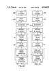
- FIG. 38 Another embodiment of a variable color display typewriter, disclosed in FIG. 38 in somewhat simplified form, is controlled by a CPU (Central Processing Unit) 470, which may include a microprocessor, microcomputer, or like device for processing a program of instructions.
- the instructions for controlling CPU 470 and tables of certain codes are stored in a program memory 408a.
- CPU 470 communicates with other devices over a data bus 472 and stores temporary data in a memory 408b.
- the operation of the typewriter will be outlined only briefly, with emphasis on the novel features provided by the invention.
- CPU 470 scans keyboard 411 in cyclic sequence and reads back data indicative of the activity of keyboard 411.
- CPU 470 When CPU 470 receives data indicating that a key has been actuated, it stops the scanning process and uses the received data to fetch from program memory 408a, which contains the table of codes for all keys, the code for the character corresponding to the actuated key, so it could be displayed and printed. CPU 470 then accesses display controller 473, for causing the character to be displayed on typewriter display 449, and print control 407, via appropriate I/O port 475, for causing the character to be imprinted by print element 405.
- the invention resides in the addition of a color memory 434, color control 50, and certain software instructions for measuring typing speed and for controlling the color of typewriter display 449 accordingly.
- CPU 470 repeatedly measures time necessary for typing a group of characters (e.g., 10 characters), by using timing control 477.
- the values of the typing speed limits, in words per minute, in the third columns were calculated by dividing constant 120 by particular times for 10 characters, in seconds, in the first columns.
- the constant 120 was obtained by dividing 600 (10 characters multiplied by 60 seconds) by 5 (5 characters per word), to obtain the number of 5-letter words per minute.
- the values of typing speed limits were rounded in the interest of simplifying the disclosure. It is readily apparent that the principles of the invention are equally applicable to other methods of measuring typing speed.
- CPU 470 compares the measured value with predetermined time limits, defining a plurality of time ranges, to determine in which time range the measured value lies. In accordance with such determination, CPU 470 then fetches from program memory 408a, which contains the table of codes for all time ranges, the binary code defining a particular color of typewriter display 449 corresponding to the determined time range, and conveys the code to color memory 434 to be stored therein, until the next time measurement is completed, and thence applied to color control 50 for illuminating typewriter display 449 in the selected color.
- CPU 470 when CPU 470 measures the time for the typing of the 10 character group to be 4.2 seconds, it will be determined that this value lies in the time range 6 to 3 seconds (CHART 3, line 2), which corresponds to typing speed range 20 to 40 words per minute.
- CPU 470 accordingly selects binary code 010 and conveys the code to color memory 436a shown in detail in FIG. 39. It is readily apparent that the binary code, when latched in color memory 436a, drives the color control line Y to a high logic level, to thereby cause typewriter display 449a, shown in detail in FIG. 45, to be illuminated in yellow color.
- CPU 470 when CPU 470 measures time for the typing of the 10 character group to be 2.8 seconds, it will be determined that this value lies in the time range 3 to 2.4 seconds (CHART 4, line 4), which corresponds to typing speed range 40 to 50 words per minute.
- CPU 470 accordingly selects and conveys to the color memory 436b, shown in detail in FIG. 40, binary code 0001000. It is readily apparent that the binary code, when latched in color memory 436b, drives the color control line G to a high logic level, to thereby cause typewriter display 449b, shown in detail in FIG. 46, to be illuminated in green color.
- composition of software commanding CPU 470 to measure typing speed and to control the color of typewriter display 449 accordingly would be within the scope of ordinary skill.
- typewriter display 449 is illuminated in one of three possible colors in accordance with the measured typing speed, comparably with CHART 1.
- typewriter display 449 is illuminated in one of seven possible colors in accordance with the measured typing speed, comparably with CHART 2.
- color memory 436a In a detail of color memory 436a shown in FIG. 39, three least significant data bus lines D0, D1, and D2 are applied to like inputs of color memory 436a and may be latched therein by a suitable transition on the data line D7.
- the need for latching is dictated by the fact that data bus 472, viewed in FIG. 38, may carry at other times signals for other devices.
- the latched data appear at the outputs Q0, Q1, and Q2 as color control signals R, Y, and G, which may be applied to like color control inputs R, Y, and G of typewriter display 449a shown in FIG. 45.
- seven least significant data bus lines D0 to D6 are applied to like inputs of color memory 436b and may be latched therein by a suitable transition on the data line D7.
- the latched data appear at the outputs Q0 to Q6 as color control signals R, W, Y, G, BG, P, and B, which may be applied to like color control inputs R, W, Y, G, BG, P, and B of typewriter display 449b shown in FIG. 46.
- CPU 470 At the completion of each time measurement of a group of 10 characters, conveys the measured value directly to color memory 434, viewed in FIG. 38, to be used as an address for the color converter memory which contains data representing the values of primary colors for all possible measured time values.
- the data bus lines D0 to D7 are applied to corresponding inputs of color memory 436a and may be latched therein by a suitable signal at its input CP.
- the latched data appear at the outputs Q0 to Q7 and thence are respectively applied to the address inputs A0 to A7 of memory 77, which contains data representing the portions of red color for all possible input combinations.
- the memory outputs D0 to D7 may be applied as shown in FIG. 17, to develop control signals RB and GB, which may be applied to like bus control inputs RB and GB of typewriter display 449c shown in FIG. 47.
- the data bus lines D0 to D7 are applied to interconnected address inputs A0 to A7 of red memory 77a, green memory 77b, and blue memory 77c, which contain data representing the portions of red, green, and blue primary colors, respectively, for all possible input combinations, as explained previously.
- the memory outputs D0 to D7 may be connected as shown in FIG. 19, to develop control signals RB, GB, and BB, which may be applied to like bus control inputs RB, GB, and BB of typewriter display 449d shown in FIG. 48.
- FIG. 43 Another embodiment of a variable color display typewriter, shown in FIG. 43, is additionally equipped with a dictionary 427 containing suitably arranged words for verification of spelling.
- the dictionary 427 may reside in a suitable memory, such as a ROM or magnetic disk.
- CPU 470 is employed verifying the accuracy of typed words. Since the operation of spelling checkers is well known, it will not be described in detail. It will suffice to state that CPU 470 identifies a group of typed characters as a word by noting word separators, such are space, comma, period, question mark, exclamation mark, and the like, and eliminates one letter words and other than fully alphabetic words. CPU 470 then attempts to find the instant typed word in dictionary 427. If the word is found, it is assumed to be spelled correctly; if it is not found, it is assumed to be incorrect - either misspelled or unknown.
- the invention resides in the method of displaying the typed text when an incorrectly typed word is detected.
- the method can be as unsophisticated as merely changing the color of typewriter display 449 when an incorrectly typed word is detected, or it may involve more complex decisions based on the number of spelling errors, complexity of the particular word, and the like.
- typewriter display 449 when the instant measured typing speed is 50 words per minute, typewriter display 449 is illuminated in green color. When an incorrectly typed word is detected under such conditions, the color of typewriter display 449 is changed to yellow for the remainder of the measurement period.
- CPU 470 when an incorrectly typed word is detected while typewriter display 449 is illuminated in purple color, which indicates typing speed between 61 to 70 words per minute, CPU 470 sends data to color memory 434 for changing the color of typewriter display 449 to blue-green for the remainder of the measurement period, to effectively decrease the indicated typing speed. It would be obvious to those skilled in the art, in the view of this disclosure, how to compose software commanding CPU 470 to modify the color of typewriter display 449 in accordance with the detection of incorrectly typed words.
- the typewriter of this invention includes substantially conventional keyboard 411, having keys representing individual alphanumeric characters, and platen 403, which may be enclosed in a suitable frame 402.
- typewriter display 449 is formed of a plurality of variable color display elements mounted in a side by side relation such that typed text may be visually presented in a substantially conventional manner.
- typewriter display 449 may be, alternatively, located adjacent to the typewriter or even remotely.
- the display elements 46e, 46f to 46n use variable color display segments 1 arranged in 7 rows by 5 columns dot matrices 1e, 1f to 1n, which may be selectively energized in different combinations to display all known alpha-numeric characters.
- the color control inputs R, Y, and G of associated color controls 52e, 52f to 52n are respectively interconnected for controlling the color of all display elements 46e, 46f to 46n uniformly in three steps. All enable inputs E are grounded to permit display elements 46e, 46f to 46n to be illuminated.
- display elements 47e, 47f to 47n use variable color display segments 1 similarly arranged in dot matrices 1e, 1f to 1n.
- the color control inputs B, P, BG, G, Y, W, and R of associated color controls 53e, 53f to 53n are respectively interconnected in a comparable fashion for controlling the color of all display elements 47e, 47f to 47n uniformly in seven steps.
- bus control inputs RB and GB of all display elements 46e, 46f to 46n are respectively interconnected for uniformly controlling their color substantially continuously. It would be obvious to those skilled in the art that suitable buffers may be used, if needed, to ensure that the bus driving circuits are not overloaded. All enable inputs E are grounded to allow all display elements 46e, 46f to 46n to be illuminated.
- bus control inputs RB, GB, and BB of all display elements 47e, 47f to 47n are respectively interconnected for uniformly controlling their color substantially continuously.
- the invention describes a method and apparatus, in a variable color display typewriter, for simultaneously displaying typed text and indicating typing speed and accuracy, by visually presenting the typed text in a color variable in accordance with the typing speed and accuracy.
Abstract
A typewriter with variable color display visually presents typed text in a color variable in accordance with the typing speed and accuracy.
Description
This is a division of my copending application Ser. No. 07/150,913, filed on Feb. 1, 1988, entitled Variable Color Display Typewriter, now U.S. Pat. No. 4,824,269 issued on Apr. 25, 1989, which is a continuation of my application Ser. No. 06/839,626, filed on Mar. 14, 1986, entitled Variable Color Display Typewriter, now abandoned.
Reference is also made to my related applications Ser. No. 06/817,114, filed on Jan. 8, 1986, entitled Variable Color Digital Timepiece, now U.S. Pat. No. 4,647,217 issued on Mar. 3, 1987, Ser. No. 06/819,111, filed on Jan. 15, 1986, entitled Variable Color Digital Multimeter, now U.S. Pat. No. 4,794,383 issued on Dec. 27, 1988, Ser. No. 06/839,526, filed on Mar. 14, 1986, entitled Variable Color Display Telephone, now U.S. Pat. No. 4,726,059 issued on Feb. 16, 1988, and Ser. No. 07/000,478, filed on Jan. 5, 1987, entitled Variable Color Digital Tachometer, now abandoned, which describe instruments employing variable color display devices.
1. Field of the Invention
This invention relates to typewriters utilizing variable color display.
2. Description of the Prior Art
A display device that can change color and selectively display characters described in my U.S. Pat. No. 4,086,514, issued on Apr. 25, 1978 and entitled Variable Color Display Device, includes display areas with three light emitting diodes for emitting variable portions of light signals of respectively different primary colors, which are blended within each display area to form a composite light signal.
Monochromatic display typewriters have flourished in recent years and are extensively used. Such display typewriters, however, are capable of visually presenting only the typed text. They are not capable of simultaneously indicating the typing speed and accuracy.
An electronic typewriter disclosed in U.S. Pat. No. 4,323,315, issued on Apr. 6, 1982 to Filippo Demonte et al. and entitled Electronic Typewriter with Display Device, includes a monochromatic display which is capable of displaying characters with different kinds of emphasis.
A microprocessor-based display controller for 5×7 matrix monochromatic display is described in Hewlett-Packard application note 1001, pages 398-413, issued in 1980 and entitled Interfacing the HDSP-2000 to Microprocessor Systems.
A device for indicating typing speed and rhythm disclosed in U.S. Pat. No. 2,717,688, issued on Sept. 13, 1955 to James A. Brooks and entitled Typing Speed and Rhythm Indicating Apparatus for Typewriters, includes a light bulb which remains continuously lit when the typist keeps depressing keys with sufficient speed and uniformity.
An electronic typewriter described in West German Patent No. 3,534,569, issued on Apr. 3, 1986 to O. Flugel et al. and entitled Electronic Typewriter with Print Speed Monitoring, includes a monochromatic display for digitally indicating typing speed.
A word processing system disclosed in U.S. Pat. No. 4,136,395, issued on Jan. 23, 1979 to Robert A. Kolpek et al. and entitled System for Automatically Proofreading a Document, includes a dictionary memory and comparator for detecting spelling errors.
In a broad sense, it is the principal object of this invention to provide a typewriter with a variable color display.
The invention endeavors to overcome problems of the prior art display typewriters by providing a new type of a display typewriter.
In the preferred embodiment is disclosed a variable color display typewriter that visually presents typed text in a color variable in accordance with the typing speed.
It is another object of the invention to provide a variable color display typewriter that visually presents typed text in a color variable in accordance with the typing accuracy.
Such typewriter is ideally suited for professional typists and for those who strive to improve and polish their typing skills.
In the drawings in which are shown several possible embodiments of the invention,
FIG. 1 is a block diagram of 2-primary color display system.
FIG. 2 is a block diagram of 3-primary color display system.
FIG. 3 is an enlarged detail of one digit of 2-primary color digital display.
FIG. 4 is an enlarged cross-sectional view of one display segment in FIG. 3, taken along the line 4--4.
FIG. 5 is an enlarged detail of one digit of 3-primary color digital display.
FIG. 6 is an enlarged cross-sectional view of one display segment in FIG. 5, taken along the line 6--6.
FIG. 7 is a schematic diagram of one 2-primary color display element.
FIG. 8 is a schematic diagram of one 3-primary color display element.
FIG. 9 is a simplified schematic diagram, similar to FIG. 7, showing how number `7` can be displayed in three different colors.
FIG. 10 is a simplified schematic diagram, similar to FIG. 8, showing how number `1` can be displayed in seven different colors.
FIG. 11 is a block diagram of 2-primary color 4-digit display.
FIG. 12 is a block diagram of 3-primary color 4-digit display.
FIG. 13 is an expanded block diagram of 2-LED color converter.
FIG. 14 is an expanded block diagram of 3-LED color converter.
FIG. 15 is a schematic diagram of a scaling circuit.
FIG. 16 is a schematic diagram of an A/D converter and memory combination of FIGS. 13 and 14.
FIG. 17 is a schematic diagram of a memory and color converter combination of FIG. 13.
FIG. 18 is a timing diagram of the circuit shown in FIG. 17.
FIG. 19 is a schematic diagram of a memory and color converter combination of FIG. 14.
FIG. 20 is a timing diagram of the circuit shown in FIG. 19.
FIG. 21 is a continuation of the timing diagram of FIG. 20.
FIG. 22 is a graphic representation of TABLE 1.
FIG. 23 is a graphic representation of TABLE 2.
FIG. 24 is a graph of the ICI chromaticity diagram.
FIG. 25 is a general block diagram of a variable color display typewriter wherein the color of the display is variable in accordance with the typing speed.
FIG. 26 is a general block diagram of a variable color display typewriter wherein the color of the display is variable in accordance with the typing accuracy.
FIG. 27 is an expanded block diagram of a variable color display typewriter shown in FIG. 25.
FIG. 28 is an expanded block diagram of a variable color display typewriter shown in FIG. 26.
FIG. 29 is an expanded diagram of a typing speed converter for controlling the color of the typewriter display in steps.
FIG. 30 is an expanded diagram of a like typing speed converter for controlling the color of the typewriter display continuously.
FIG. 31 is a timing diagram showing the relationship between the measured typing speed and generated COUNTER SAVE and COUNTER CLEAR signals.
FIG. 32 is a detail of the combination of the counter shown generally in FIG. 30 with a memory for 2-primary color converter.
FIG. 33 is a detail of the combination of the counter shown generally in FIG. 30 with a memory for 3-primary color converter.
FIG. 34 is a schematic diagram of a circuit for generating COUNTER SAVE and COUNTER CLEAR signals.
FIG. 35 is a schematic diagram of an oscillator shown generally in FIGS. 29 and 30.
FIG. 36 is a detail of the counter and decoder combination shown generally in FIG. 29 for controlling the color of the typewriter display in three steps.
FIG. 37 is a detail of the counter and decoder combination shown generally in FIG. 29 for controlling the color of the typewriter display in seven steps.
FIG. 38 is a block diagram of a variable color display typewriter controlled by a central processor.
FIG. 39 is a detail of the color memory of FIG. 38 for controlling the color of the typewriter display in three steps.
FIG. 40 is a like detail of the color memory of FIG. 38 for controlling the color of the typewriter display in seven steps.
FIG. 41 is a detail of the color memory of FIG. 38 used in a 2-LED continuously variable color converter.
FIG. 42 is a detail of the color memory of FIG. 38 used in a 3-LED continuously variable color converter.
FIG. 43 is a block diagram of a CPU controlled variable color display typewriter with spelling checker.
FIG. 44 is a top view of a variable color display typewriter of the present invention.
FIG. 45 is a detail of a variable color typewriter display showing the interconnection of three step variable color display elements.
FIG. 46 is a detail of a variable color typewriter display showing the interconnection of seven step variable color display elements.
FIG. 47 is a detail of a variable color typewriter display showing the interconnection of continuously variable color 2-LED display elements.
FIG. 48 is a detail of a variable color typewriter display showing the interconnection of continuously variable color 3-LED display elements.
Throughout the drawings, like characters indicate like parts.
In the tables which show examples of a relationship between an input voltage, memory contents, and resulting color in the color converter of the present invention,
TABLE 1 shows the characteristic of a step variable 2-primary color converter.
TABLE 2 shows a rainbow-like characteristic of a continuously variable 3-primary color converter.
Throughout the tables, memory addresses and data are expressed in a well known hexadecimal notation.
In the charts which show examples of the relationship between the measured typing speed and resulting color of the typewriter display,
Referring now, more particularly, to the drawings, in FIG. 1 is shown a block diagram of a 2-primary color display system including a display decoder 21, a variable color 2-LED display element 46, and a 2-primary color control 52. The display decoder 21 accepts at its inputs a code representing the character to be displayed and accordingly develops output drive signals to drive respective segments of display element 46. The color control 52 accepts color control signals at its inputs R (red), Y (yellow), and G (green) and develops at its outputs drive signals for red bus 5 and green bus 6, respectively, to illuminate display element 46 in a selected color.
In FIG. 2 is shown a block diagram of a 3-primary color display system including a display decoder 21, a variable color 3-LED display element 47, and a 3-primary color control 53. The color control 53 accepts color control signals at its inputs R (red), Y (yellow), G (green), BG (blue-green), B (blue), P (purple), and W (white) and develops at its outputs drive signals for red bus 5, green bus 6, and blue bus 7, respectively, to illuminate display element 47 in a selected color.
In FIG. 3, the 2-primary color display element 46 includes seven elongated display segments a, b, c, d, e, f, and g, arranged in a conventional pattern, which may be selectively energized in different combinations to display the desired digits. Each display segment includes a pair of LEDs (light emitting diodes): red LED 2 and green LED 3, which are closely adjacent such that the light signals emitted therefrom are substantially superimposed upon each other to mix the colors. To facilitate the illustration, the LEDs are designated by segment symbols, e.g., the red LED in the segment a is designated as 2a, etc.
In FIG. 4, red LED 2e and green LED 3e are placed on the base of a segment body 15a which is filled with a transparent light scattering material 16. When forwardly biased, LEDs 2e and 3e emit light signals of red and green colors, respectively, which are scattered within transparent material 16, thereby blending the red and green light signals into a composite light signal that emerges at the upper surface of segment body 15a. The color of the composite light signal may be controlled by varying the portions of the red and green light signals.
In FIG. 5, each display segment of the 3-primary color display element 47 includes a triad of LEDs: red LED 2, green LED 3, and blue LED 4, which are closely adjacent such that the light signals emitted therefrom are substantially superimposed upon one another to mix the colors.
In FIG. 6, red LED 2e, green LED 3e, and blue LED 4e are placed on the base of a segment body 15b which is filled with a transparent light scattering material 16. Red LEDs are typically manufactured by diffusing a p-n junction into a GaAsP epitaxial layer on a GaAs substrate; green LEDs typically use a GaP epitaxial layer on a GaP substrate; blue LEDs are typically made from SiC material.
When forwardly biased, LEDs 2e, 3e, and 4e emit light signals of red, green, and blue colors, respectively, which are scattered within transparent material 16, thereby blending the red, green, and blue light signals into a composite light signal that emerges at the upper surface of segment body 15b. The color of the composite light signal may be controlled by varying the portions of the red, green, and blue light signals.
In FIG. 7 is shown a schematic diagram of a 2-primary color common cathodes 7-segment display element 42 which can selectively display various digital fonts in different colors on display segments a, b, c, d, e, f, g, and DP (Decimal Point). The anodes of all red and green LED pairs are interconnected in each display segment and are electrically connected to respective outputs of a commercially well known common-cathode 7-segment decoder driver 23. The cathodes of all red LEDs 2a, 2b, 2c, 2d, 2e, 2f, 2g, and 2i are interconnected to a common electric path referred to as a red bus 5. The cathodes of all green LEDs 3a, 3b, 3c, 3d, 3e, 3f, 3g, and 3i are interconnected to a like common electric path referred to as a green bus 6.
The red bus 5 is connected to the output of a tri-state inverting buffer 63a, capable of sinking sufficient current to forwardly bias all red LEDs 2a to 2i in display element 42. The green bus 6 is connected to the output of a like buffer 63b. The two buffers 63a and 63b can be simultaneously enabled by applying a low logic level signal to the input of inverter 64a, and disabled by applying a high logic level signal thereto. When buffers 63a and 63b are enabled, the conditions of red bus 5 and green bus 6 can be selectively controlled by applying suitable logic control signals to the bus control inputs RB (red bus) and GB (green bus), to illuminate display element 42 in a selected color. When buffers 63a and 63b are disabled, both red bus 5 and green bus 6 are effectively disconnected to cause display element 42 to be completely extinguished.
In FIG. 8 is shown a schematic diagram of a 3-primary color common anodes 7-segment display element 43 which can selectively display digital fonts in different colors. The cathodes of all red, green, and blue LED triads in each display segment are interconnected and electrically connected to respective outputs of a commercially well know common anode 7-segment decoder driver 24. The anodes of all red LEDs 2a, 2b, 2c, 2d, 2e, 2f, and 2g are interconnected to form a common electric path referred to as a red bus 5. The anodes of all green LEDs 3a, 3b, 3c, 3d, 3e, 3f, and 3g are interconnected to form a like common electric path referred to as a green bus 6. The anodes of all blue LEDs 4a, 4b, 4c, 4d, 4e, 4f, and 4g are interconnected to form a like common electric path referred to as a blue bus 7.
The red bus 5 is connected to the output of a non-inverting tri-state buffer 62a, capable of sourcing sufficient current to illuminate all red LEDs 2a to 2g in display element 43. The green bus 6 is connected to the output of a like buffer 62b. The blue bus 7 is connected to the output of a like buffer 62c. The three buffers 62a, 62b, and 62c can be simultaneously enabled, by applying a low logic level signal to the input of inverter 64b, and disabled by applying a high logic level signal thereto. When buffers 62a, 62b, and 62c are enabled, the conditions of red bus 5, green bus 6, and blue bus 7 can be selectively controlled by applying valid combinations of logic level signals to the bus control inputs RB (red bus), GB (green bus), and BB (blue bus), to illuminate display element 43 in a selected color. When buffers 62a, 62b, and 62c are disabled, red bus 5, green bus 6, and blue bus 7 are effectively disconnected to cause display element 43 to be completely extinguished.
The operation of display element 42 shown in FIG. 7 will be now explained by the example of illuminating a digit `7` in three different colors. A simplified schematic diagram to facilitate the explanation is shown in FIG. 9. Any digit between 0 and 9 can be selectively displayed by applying the appropriate BCD code to the inputs A0, A1, A2, and A3 of common-cathode 7-segment decoder driver 23. The decoder driver 23 develops at its outputs a, b, c, d, e, f, g, and DP drive signals for energizing selected groups of the segments to thereby visually display the selected number, in a manner well known to those having ordinary skill in the art. To display decimal number `7`, a BCD code 0111 is applied to the inputs A0, A1, A2, and A3. The decoder driver 23 develops high voltage levels at its outputs a, b, and c, to illuminate equally designated segments a, b, and c, and low voltage levels at all remaining outputs (not shown), to extinguish all remaining segments d, e, f, and g.
To illuminate display element 42 in red color, the color control input R is raised to a high logic level, and the color control inputs Y and G are maintained at a low logic level. As a result, the output of OR gate 60a rises to a high logic level, thereby causing the output of buffer 63a to drop to a low logic level. The current flows from the output a of decoder driver 23, via red LED 2a and red bus 5, to current sinking output of buffer 63a. Similarly, the current flows from the output b of decoder driver 23, via red LED 2b and red bus 5, to the output of buffer 63a. The current flows from the output c of decoder driver 23, via red LED 2c and red bus 5, to the output of buffer 63a. As a result, segments a, b, and c illuminate in red color, thereby causing a visual impression of a character `7`. The green LEDs 3a, 3b, 3c remain extinguished because the output of buffer 63b is at a high logic level, thereby disabling green bus 6.
To illuminate display element 42 in green color, the color control input G is raised to a high logic level, while the color control inputs R and Y are maintained at a low logic level. As a result, the output of OR gate 60b rises to a high logic level, thereby causing the output of buffer 63b to drop to a low logic level. The current flows from the output a of decoder driver 23, via green LED 3a and green bus 6, to current sinking output of buffer 63b. Similarly, the current flows from the output b of decoder driver 23, via green LED 3b and green bus 6, to the output of buffer 63b. The current flows from the output c of decoder driver 23, via green LED 3c and green bus 6, to the output of buffer 63b. As a result, segments a, b, and c illuminate in green color. The red LEDs 2a, 2b, and 2c remain extinguished because the output of buffer 63a is at a high logic level, thereby disabling red bus 5.
To illuminate display element 42 in yellow color, the color control input Y is raised to a high logic level, while the color inputs R and G are maintained at a low logic level. As a result, the outputs of both OR gates 60a and 60b rise to a high logic level, thereby causing the outputs of both buffers 63a and 63b to drop to a low logic level. The current flows from the output a of decoder driver 23, via red LED 2a and red bus 5, to current sinking output of buffer 63a, and, via green LED 3a and green bus 6, to current sinking output of buffer 63b. Similarly, the current flows from the output b of decoder driver 23, via red LED 2b and red bus 5, to the output of buffer 63a, and, via green LED 3b and green bus 6, to the output of buffer 63b. The current flows from the output c of decoder driver 23, via red LED 2c and red bus 5, to the output of buffer 63a, and, via green LED 3c and green bus 6, to the output of buffer 63b. As a result of blending light of red and green colors in each segment, segments a, b, and c illuminate in substantially yellow color.
The operation of display element 43 shown in FIG. 8 will be now explained by the example of illuminating a digit `1` in seven different colors. A simplified schematic diagram to facilitate the explanation is shown in FIG. 10. To display decimal number `1`, a BCD code 0001 is applied to the inputs A0, A1, A2, and A3 of common anode 7-segment decoder driver 24. The decoder driver 24 develops low voltage levels at its outputs b and c, to illuminate equally designated segments b and c, and high voltage levels at all remaining outputs (not shown), to extinguish all remaining segments a, d, e, f, and g.
To illuminate display element 43 in red color, the color control input R is raised to a high logic level, while all remaining color control inputs are maintained at a low logic level. As a result, the output of OR gate 61a rises to a high logic level, thereby causing the output of buffer 62a to rise to a high logic level. The current flows from the output of buffer 62a, via red bus 5 and red LED 2b, to the output b of decoder driver 24, and, via red LED 2c, to the output c of decoder driver 24. As a result, segments b and c illuminate in red color, thereby causing a visual impression of a character `1`. The green LEDs 3b, 3c and blue LEDs 4b, 4c remain extinguished because green bus 6 and blue bus 7 are disabled.
To illuminate display element 43 in green color, the color control input G is raised to a high logic level, while all remaining color control inputs are maintained at a low logic level. As a result, the output of OR gate 61b rises to a high logic level, thereby causing the output of buffer 62b to rise to a high logic level. The current flows from the output of buffer 62b, via green bus 6 and green LED 3b, to the output b of decoder driver 24, and, via green LED 3c, to the output c of decoder driver 24. As a result, segments b and c illuminate in green color.
To illuminate display element 43 in blue color, the color control input B is raised to a high logic level, while all remaining color control inputs are maintained at a low logic level. As a result, the output of OR gate 61c rises to a high logic level, thereby causing the output of buffer 62c to rise to a high logic level. The current flows from the output of buffer 62c, via blue bus 7 and blue LED 4b, to the output b of decoder driver 24, and, via blue LED 4c, to the output c of decoder driver 24. As a result, segments b and c illuminate in blue color.
To illuminate display element 43 in yellow color, the color control input Y is raised to a high logic level, while all remaining color control inputs are maintained at a low logic level. As a result, the outputs of OR gates 61a and 61b rise to a high logic level, thereby causing the outputs of buffers 62a and 62b to rise to a high logic level. The current flows from the output of buffer 62a, via red bus 5 and red LED 2b, to the output b of decoder driver 24, and, via red LED 2c, to the output c of decoder driver 24. The current also flows from the output of buffer 62b, via green bus 6 and green LED 3b, to the output b of decoder driver 24, and, via green LED 3c, to the output c of decoder driver 24. As a result of blending light of red and green colors in each segment, the segments b and c illuminate in substantially yellow color.
To illuminate display element 43 in purple color, the color control input P is raised to a high logic level, while all remaining color control inputs are maintained at a low logic level. As a result, the outputs of OR gates 61a and 61c rise to a high logic level, thereby causing the outputs of buffers 62a and 62c to rise to a high logic level. The current flows from the output of buffer 62a, via red bus 5 and red LED 2b, to the output b of decoder driver 24, and, via red LED 2c, to the output c of decoder driver 24. The current also flows from the output of buffer 62c, via blue bus 7 and blue LED 4b, to the output b of decoder driver 24, and, via blue LED 4c, to the output c of decoder driver 24. As a result of blending light of red and blue colors in each segment, segments b and c illuminate in substantially purple color.
To illuminate display element 43 in blue-green color, the color control input BG is raised to a high logic level, while all remaining color control inputs are maintained at a low logic level. As a result, the outputs of OR gates 61b and 61c rise to a high logic level, thereby causing the outputs of buffers 62b and 62c to rise to a high logic level. The current flows from the output of buffer 62b, via green bus 6 and green LED 3b, to the output b of decoder driver 24, and, via green LED 3c, to the output c of decoder driver 24. The current also flows from the output of buffer 62c, via blue bus 7 and blue LED 4b, to the output b of decoder driver 24, and, via blue LED 4c, to the output c of decoder driver 24. As a result of blending light of green and blue colors in each segment, segments b and c illuminate in substantially blue-green color.
To illuminate display element 43 in white color, the color control input W is raised to a high logic level, while all remaining color control inputs are maintained at a low logic level. As a result, the outputs of OR gates 61a, 61b, and 61c rise to a high logic level, thereby causing the outputs of respective buffers 62a, 62b, and 62c to rise to a high logic level. The current flows from the output of buffer 62a, via red bus 5 and red LED 2b, to the output b of decoder driver 24, and, via red LED 2c, to the output c of decoder driver 24. The current also flows from the output of buffer 62b, via green bus 6 and green LED 3b, to the output b of decoder driver 24, and, via green LED 3c, to the output c of decoder driver 24. The current also flows from the output of buffer 62c, via blue bus 7 and blue LED 4b, to the output b of decoder driver 24, and, via blue LED 4c, to the output c of decoder driver 24. As a result of blending light of red, green, and blue colors in each segment, segments b and c illuminate in substantially white color.
Since the outputs of decoder driver 24 may be overloaded by driving a triad of LEDs in parallel in display element 43, rather than a single LED in a monochromatic display, it would be obvious to employ suitable buffers to drive respective color display segments (not shown).
To illustrate how the present invention can be utilized in a multi-element variable color display configuration, in FIG. 11 is shown a detail of the interconnection in a 2-primary color 4-digit display having display segments 1a, 1b, 1c, and 1d arranged in a 7-segment font. The color control inputs R, Y, and G of color controls 52a, 52b, 52c, and 52d of all display elements 46a, 46b, 46c, and 46d are interconnected, respectively, and enable inputs E1, E2, E3, and E4 are used to control the conditions of respective display elements 46a, 46b, 46c, and 46d. A high logic level at the enable input E extinguishes the particular display element 46a, 46b, 46c, or 46d; a low logic level therein illuminates display element 46a, 46b, 46c, or 46d in a color determined by the instant conditions of the color control inputs R, Y, and G.
In FIG. 12 is shown a like detail of the interconnection in a 3-primary color 4-digit display having display segments 1a, 1b, 1c, and 1d arranged in a 7-segment font. Similarly, the color control inputs B, P, BG, G, Y, W, and R of color controls 53a, 53b, 53c, and 53d of all display elements 47a, 47b, 47c, and 47d are interconnected, and the conditions of respective display elements 47a, 47b, 47c, and 47d are controlled by enable inputs E1, E2, E3, and E4. A high logic level at the enable input E extinguishes the particular display element 47a, 47b, 47c, or 47d; a low logic level therein illuminates display element 47a, 47b, 47c, or 47d in a color determined by the instant conditions of the color control inputs B, P, BG, G, Y, W, and R.
The exemplary color control circuits described herein will cooperate equally well with a multi-element variable color display constructed either in common cathodes or in common anodes configuration.
The display system shown in FIG. 13 utilizes a scaling circuit 80a which scales input analog voltage levels to a voltage range suitable for an A/D converter 74a, which in turn develops at its outputs a digital code having relation to the value of the input analog voltage. The output lines of A/D converter 74a are connected to the address inputs of a memory 76 having a plurality of addressable locations which contain data indicating the portions of red color for several different values of the input analog voltage. The output data of memory 76 are applied to the inputs of a color converter 57 which will develop control signals for red bus 5 and green bus 6, respectively, of variable color display element 42.
The display system shown in FIG. 14 utilizes a scaling circuit 80b and an A/D converter 74b for converting the instant value of an input analog voltage to a digital code. The outputs of A/D converter 74b are connected, in parallel, to the address inputs of memory 76a, which contains data indicating the portions of red color, to the address inputs of memory 76b, which contains data indicating the portions of green color, and to the address inputs of memory 76c, which contains data indicating the portions of blue color. The output data of memory 76a are applied to red color converter 59a which will develop control signals for red bus 5 of variable color display element 43. The output data of memory 76b are applied to green color converter 59b which will develop control signals for green bus 6 of display element 43. The output data of memory 76c are applied to blue color converter 59c which will develop control signals for blue bus 7 of display element 43.
FIG. 15 is a schematic diagram of a scaling circuit capable of shifting and amplifying the input voltage levels. The circuit utilizes two operational amplifiers 81a and 81b in a standard inverting configuration. The amplifier 81a is set for a unity gain by using resistors 90a and 90b of equal values; potentiometer 92a is adjusted to set a desired offset voltage. The amplifier 81b sets the gain by adjusting feedback potentiometer 92b to a desired value with respect to resistor 90c. As a result, an input voltage, which may vary between arbitrary limits Vlow and Vhigh, may be scaled and shifted to the range between 0 Volts and 9.961 Volts, to facilitate the use of a commercially available A/D converter.
FIG. 16 is a schematic diagram of an A/D (analog-to-digital) converter 75 which is capable of converting input analog voltage, applied via resistor 90e to its input Vin, to 8-bit digital data for addressing a memory 77. The conversion may be initiated from time to time by applying a short positive pulse 99a to the Blank and Convert input B&C. A/D converter 75 will thereafter perform a conversion of the instant input voltage to 8-bit data indicative of its value. When the conversion is completed, the Data Ready output drops to a low logic level, thereby indicating that the data are available at the outputs Bit 1 to Bit 8, which are directly connected to respective address inputs A0 to A7 of memory 77. When the DATA READY output drops to a low logic level, the Chip Select input CS of memory 77 is activated, memory 77 is enabled, and the data, residing at the address selected by the instant output of A/D converter 75, will appear at its data outputs D0 to D7.
The description of the schematic diagram in FIG. 17 should be considered together with its accompanying timing diagram shown in FIG. 18. A clock signal 99b of a suitable frequency (e.g., 10 kHz), to provide a flicker-free display, is applied to the Clock Pulse inputs CP of 8-bit binary counters 71e and 71f to step them down. At the end of each counter cycle, which takes 256 clock cycles to complete, the Terminal Count output TC of counter 71e drops to a low logic level for one clock cycle, to thereby indicate that the lowest count was reached. The negative pulse 99c at the TC output of counter 71e, which is connected to the Parallel Load input PL of counter 71f, causes the instant data at the outputs of memory 76 to be loaded into counter 71f. The data at memory 76 represent the portion of red color; the portion of green color is complementary. The rising edge of the TC pulse 99c triggers flip-flop 73 into its set condition wherein its output Q rises to a high logic level.
The counter 71f will count down, from the loaded value, until it reaches zero count, at which moment its TC output drops to a low logic level. The negative pulse at the TC output of counter 71f, which is connected to Clear Direct input CD of flip-flop 73, causes the latter to be reset and to remain in its reset condition until it is set again at the beginning of the next 256-count cycle. It is thus obvious that the Q output of flip-flop 73 is at a high logic level for a period of time proportional to the data initially loaded into counter 71f. The complementary output Q is at a high logic level for a complementary period of time.
The Q and Q outputs of flip-flop 73 are connected to red bus 5 and green bus 6, respectively, via suitable buffers 63a and 63b, shown in detail in FIG. 7, to respectively energize red bus 5 and green bus 6 for variable time periods, depending on the data stored in memory 76.
By referring now, more particularly, to the timing diagram shown in FIG. 18, in which the waveforms are compressed to facilitate the illustration, the EXAMPLE 1 considers the memory data `FD`, in a standard hexadecimal notation, to generate light of substantially red color. At the beginning of the counter cycle, pulse 99c loads data `FD` into counter 71f. Simultaneously, flip-flop 73 is set by the rising edge of pulse 99c. The counter 71f will be thereafter stepped down by clock pulses 99b, until it reaches zero count, 2 clock cycles before the end of the counter cycle. At that instant a short negative pulse 99d is produced at its output TC to reset flip-flop 73, which will remain reset for 2 clock cycles and will be set again by pulse 99c at the beginning of the next counter cycle, which will repeat the process. It is readily apparent that flip-flop 73 was set for 254 clock cycles, or about 99% of the time, and reset for 2 clock cycles, or about 1% of the time. Accordingly, red bus 5 of display element 42 is energized for about 99% of the time, and green bus 6 is energized for the remaining about 1% of the time. As a result, display element 42 illuminates in substantially red color.
The EXAMPLE 2 considers the memory data `02` (HEX) to generate light of substantially green color. At the beginning of the counter cycle, data `02` are loaded into counter 71f, and, simultaneously, flip-flop 73 is set. The counter 71f will count down and will reach zero count after 2 clock cycles. At that instant it produces at its output TC a negative pulse 99e to reset flip-flop 73. It is readily apparent that flip-flop 73 was set for 2 clock cycles, or about 1% of the time, and reset for 254 clock cycles, or about 99% of the time. Accordingly, red bus 5 of display element 42 is energized for about 1% of the time, and green bus 6 is energized for the remaining about 99% of the time. As a result, display element 42 illuminates in substantially green color.
The EXAMPLE 3 considers the memory data `80` (HEX) to generate light of substantially yellow color. At the beginning of the counter cycle, data `80` are loaded into counter 71f, and, simultaneously, flip-flop 73 is set. The counter 71f will count down and will reach zero count after 128 clock cycles. At that instant it produces at its output TC a negative pulse 99f to reset flip-flop 73. It is readily apparent that flip-flop 73 was set for 128 clock cycles, or about 50% of the time, and reset for 128 clock cycles, or about 50% of the time. Accordingly, red bus 5 of display element 42 is energized for about 50% of the time, and green bus 6 is energized for the remaining about 50% of the time. As a result of blending substantially equal portions of red and green colors, display element 42 illuminates in substantially yellow color.
The description of the schematic diagram of a 3-LED color converter in FIG. 19 should be considered together with its accompanying timing diagrams shown in FIGS. 20 and 21. A clock signal 99b is applied to the CP inputs of counters 71d, 71a, 71b, and 71c to step them down. Every 256 counts a negative pulse 99c is generated at the TC output of counter 71d, to load data into counters 71a, 71b, and 71c from respective memories 76a, 76b, and 76c, and to set flip- flops 73a, 73b, and 73c. The data in red memory 76a represent the portions of red color, the data in green memory 76b represent the portions of green color, and the data in blue memory 76c represent the portions of blue color to be blended.
The counters 71a, 71b, and 71c will count down, from the respective loaded values, until zero counts are reached. When the respective values of the loaded data are different, the length of time of the count-down is different for each counter 71a, 71b, and 71c. When a particular counter 71a, 71b, or 71c reaches zero count, its TC output momentarily drops to a low logic level, to reset its associated flip-flop (red counter 71a resets its red flip-flop 73a, green counter 71b resets its associated green flip-flop 73b, and blue counter 71c resets its associated blue flip-flop 73c). Eventually, all three flip- flops 73a, 73b, and 73c will be reset. The Q outputs of flip- flops 73a, 73b, and 73c are connected to red bus 5, green bus 6, and blue bus 7, respectively, via suitable buffers 62a, 62b, and 62c, as shown in FIG. 8, to respectively energize red bus 5, green bus 6, and blue bus 7 for variable periods of time.
By referring now more particularly to the timing diagram shown in FIGS. 20 and 21, the EXAMPLE 4 considers red memory data `80`, green memory data `00`, and blue memory data `80`, all in hexadecimal notation, to generate light of substantially purple color. At the beginning of the counter cycle, the pulse 99c simultaneously loads data `80` from red memory 76a into red counter 71a, data `00` from green memory 76b into green counter 71b, and data `80` from blue memory 76c into blue counter 71c. The counters 71a, 71b, and 71c will be thereafter stepped down. The red counter 71a will reach its zero count after 128 clock cycles; green counter 71b will reach its zero count immediately; blue counter 71c will reach its zero count after 128 clock cycles.
It is readily apparent that red flip-flop 73a was set for 128 clock cycles, or about 50% of the time, green flip-flop 73b was never set, and blue flip-flop 73c was set for 128 clock cycles, or about 50% of the time. Accordingly, red bus 5 of display element 43 is energized for about 50% of the time, green bus 6 is never energized, and blue bus 7 is energized for about 50% of the time. As a result of blending substantially equal portions of red and blue colors, display element 43 illuminates in substantially purple color.
The EXAMPLE 5 considers red memory data `00`, green memory data `80`, and blue memory data `80`, to generate light of substantially blue-green color. At the beginning of the counter cycle, data `00` are loaded into red counter 71a, data `80` are loaded into green counter 71b, and data `80` are loaded into blue counter 71c. The red counter 71a will reach its zero count immediately, green counter 71b will reach its zero count after 128 clock periods, and so will blue counter 71c.
The red flip-flop 73a was never set, green flip-flop 73b was set for 128 clock pulses, or about 50% of the time, and so was blue flip-flop 73c. Accordingly, green bus 6 of display element 43 is energized for about 50% of the time, and so is blue bus 7. As a result, display element 43 illuminates in substantially blue-green color.
The EXAMPLE 6 considers red memory data `40`, green memory data `40`, and blue memory data `80`, to generate light of substantially cyan color. At the beginning of the counter cycle, the data `40` are loaded into red counter 71a, data `40` are loaded into green counter 71b, and data `80` are loaded into blue counter 71c. The red counter 71a will reach its zero count after 64 clock cycles, and so will green counter 71b. The blue counter 71c will reach its zero count after 128 clock cycles.
The red flip-flop 73a was set for 64 clock cycles, or about 25% of the time, and so was green flip-flop 73b. The blue flip-flop 73c was set for 128 clock cycles, or about 50% of the time. Accordingly, red bus 5 and green bus 6 of display element 43 are energized for about 25% of the time, and blue bus 7 is energized for about 50% of the time. As a result of blending about 50% of blue color, 25% of red color, and 25% of green color, display element 43 illuminates in substantially cyan color.
The EXAMPLE 7 considers red memory data `80`, green memory data `40`, and blue memory data `40`, to generate light of substantially magenta color. At the beginning of the counter cycle, the data `80` are loaded into red counter 71a, data `40` are loaded into green counter 71b, and data `40` are loaded into blue counter 71c. The red counter 71a will reach its zero count after 128 clock cycles, green counter 71b will reach its zero count after 64 clock cycles, and so will blue counter 71c.
The red flip-flop 73a was set for 128 clock cycles, or about 50% of the time, green flip-flop 73b and blue flip-flop 73c were set for 64 clock cycles, or about 25% of the time. Accordingly, red bus 5 of display element 43 is energized for about 50% of the time, green bus 6 and blue bus 7 are energized for about 25% of the time. As a result, display element 43 illuminates in substantially magenta color.
By referring now more particularly to FIGS. 22 and 23, which are graphic representations of TABLES 1 and 2, respectively, the data at each memory address are digital representation of the portion of the particular primary color. All examples consider an 8-bit wide PROM (Programmable Read Only Memory). However, the principles of the invention could be applied to other types of memories.
In FIG. 22, RED PORTION indicates the portion of red primary color; GREEN PORTION indicates the portion of green primary color. The RED PORTION for a particular memory address was calculated by dividing the actual value of data residing at that address by the maximum possible data `FF` (HEX). The GREEN PORTION for the same memory address is complementary; it was obtained by subtracting the calculated value of the RED PORTION from number 1.0.
In FIG. 22 is shown the characteristic of a 2-primary color converter, defined in TABLE 1, for developing color variable in steps: pure green for input voltages less than 0.625 V, substantially yellow for voltages between 1.25 V and 1.875 V, pure red for voltages between 2.5 V and 3.125 V, and of intermediate colors therebetween, this sequence being repeated three times over the voltage range.
In FIG. 23, RED PORTION indicates the portion of red primary color; GREEN PORTION indicates the portion of green primary color; BLUE PORTION indicates the portion of blue primary color. The RED PORTION for a particular memory address was calculated by dividing the value of red data residing at such address by the maximum possible data `FF` (HEX). Similarly, the GREEN PORTION for that memory address was obtained by dividing the value of green data by `FF` (HEX). The BLUE PORTION was obtained by dividing the value of blue data by `FF` (HEX).
In FIG. 23 is shown the characteristic of a 3-primary color converter, defined in TABLE 2, for developing color continuously variable from pure red, through substantially orange and yellow, pure green, pure blue, to substantially purple, in a rainbow-like fashion.
In the examples of the characteristics of color converters shown in TABLE 1 and TABLE 2, the data values stored in red memory 76a, green memory 76b, and blue memory 76c are so designed that the sums of the red data, green data, and blue data are constant for all memory addresses, to provide uniform light intensities for all colors. It is further contemplated that data stored in red memory 76a, green memory 76b, and blue memory 76c may be modified in order to compensate for different efficiencies of red, green, and blue LEDs. By way of an example, data values for a low efficiency LED may be proportionally incremented such that time of energization is proportionally increased, to effectively provide equal luminances for LEDs of unequal efficiencies.
With reference to FIG. 24 there is shown the ICI (International Committee on Illumination) chromaticity diagram designed to specify a particular color in terms of x and y coordinates. Pure colors are located along the horseshoe-like periphery. Reference numbers along the periphery indicate wavelength in nanometers. When relative portions of three primary colors are known, the color of light produced by blending their emissions can be determined by examining the x and y values of ICI coordinates.
Turning now to FIG. 25, the variable color display typewriter of this invention includes a keyboard 411 having a plurality of keys adapted for actuation, decoder and memory 413, for interrogating keyboard 411 to detect actuated keys and for developing and storing codes corresponding to the actuated keys, print control 407, for activating a print element 405 to effect the printing of a character associated with the actuated key, and variable color display 40, for visually presenting the typed characters. The invention resides in the addition of a color control 50 for controlling the color of display 40 in accordance with output signals developed by a typing speed converter 423 and a typing accuracy converter 428. Such typewriter will visually present typed text in a color variable in accordance with both typing speed and typing accuracy.
In FIG. 26 is shown a like typewriter, characterized by a typing speed converter 423 and a spelling converter 429, which will visually present typed text in a color variable in accordance with both typing speed and correct spelling of typed words.
The preferred embodiment of the invention is illustrated in FIG. 27 in a block diagram configuration so as not to obscure the invention by unnecessary details. As keyboard 411, keyboard encoder 415, display memory 409, print control 407, and print element 405 may be substantially conventional, their operation will not be described in detail. The invention resides in the addition of typing speed converter 423 and associated circuitry for measuring the typing speed and for controlling the color of typewriter display 449 accordingly. When a particular key of keyboard 411 is actuated, keyboard encoder 415 develops at its DATA outputs a code corresponding to the actuated key and at its DATA READY output a positive going pulse indicating that the code is valid. When another key is actuated, new code appears at the DATA outputs and another pulse is produced at the DATA READY output. The typing speed converter 423 counts the DATA READY pulses during predetermined time intervals defined by a time base 425. The characters typed into display memory 409 may be visually presented on typewriter display 449 in a substantially conventional manner (not shown).
FIG. 28 is a block diagram of a similar circuit characterized by a spelling checker 430 with associated dictionary 427 of words for checking typed text for accuracy. The typed text will be visually presented on typewriter display 449 in a color variable in accordance with the typing accuracy.
The typing speed converter 423 illustrated in FIG. 29 includes a counter 450 responsive to pulses that appear at the DATA READY output of keyboard encoder 415, an oscillator 455 for furnishing a periodic sequence of clock pulses of a predetermined frequency, counter control 437 for starting and stopping counter 450 such that its accumulated count is proportional to the instant typing speed, as will be more fully explained later, color control latch 435 for assuming, when enabled, the count accumulated in counter 450, and step variable color control 51 for developing color control signals accordingly.
A like typing speed converter 423' shown in FIG. 30 differs from the one in FIG. 29 in that a continuously variable color converter 56 is used in lieu of step variable color control 51. When counter 450 completes its counting cycle, its output data are intermediately stored in color control latch 435 and thence applied to the input of color converter 56 for developing color bus driving signals accordingly.
By referring now to the timing diagram shown in FIG. 31, the typing speed measuring method may be briefly explained. In essence, the number of pulses 499b that appear at the DATA READY output of keyboard encoder 415 is counted during predetermined time intervals defined by adjacent COUNTER SAVE positive going edges 499e of stable clock pulses 499a, and the instant typing speed is calculated therefrom. The COUNTER SAVE edge 499e is also used to trigger a negative AUX PULSE 499c of a short duration, which in turn is used to trigger a short negative COUNTER CLEAR pulse 499d. In practice, the COUNTER SAVE edge 499e is used to effect the transfer of the instant count of counter 451, representing the number of typed characters during the measurement interval, to its output register, viewed in FIG. 32. Immediately after that, counter 451 will be restored to its initial condition by COUNTER CLEAR pulse 499d and will start accumulating pulses 499b again to repeat the measurement. The instant typing speed may be calculated by multiplying the accumulated count by the clock frequency, to obtain the number of typed characters per second, and then by 12 (60 divided by 5), to obtain the number of 5-letter words per minute, in accordance with the official typing rules. It would be appreciated by persons skilled in the art that the principles of the invention are also applicable to other methods of typing speed measurement.
FIG. 32 is a detail of the combination of 8-bit binary counter with output register 451 and PROM 77. The counter 451 may be from time to time reset to its zero count by applying a short negative COUNTER CLEAR pulse to its Clear input CLR. When not in its reset condition, counter 451 is incremented by pulses 499b that appear at the DATA READY output of keyboard encoder 415. When the COUNTER SAVE signal appears at the Register Clock input REG CL of counter 451, the instant accumulated count data are transferred to its output register and appear at the outputs Q0 to Q7, which are directly connected to respective address inputs A0 to A7 of memory 77 which contains data representing the portions of red color for all possible output data of counter 451. The memory data residing at the address selected by the instant output data of counter 451 will appear at the memory outputs D0 to D7, which may be connected as shown in the detail in FIG. 17 to develop bus control signals RB and GB, which may be applied to like inputs shown in FIG. 47, to cause typewriter display 449c to illuminate in a specific color.
In FIG. 33 is shown a similar schematic diagram of the combination of 8-bit binary counter with output register 451 with red memory 77a, green memory 77b, and blue memory 77c. The outputs Q0 to Q7 of counter 451 are respectively connected to interconnected address inputs A0 to A7 of red memory 77a, green memory 77b, and blue memory 77c. When the instant output data of counter 451 are applied to the address inputs of memories 77a, 77b, and 77c, the memory data residing at such address in memory 77a, representing the portion of red primary color, appear at its memory outputs D0 to D7, memory data residing at the same address in memory 77b, representing the portion of green primary color, appear at its memory outputs D0 to D7, and memory data residing at the same address in memory 77c, representing the portion of blue primary color, appear at its memory outputs D0 to D7. The memory outputs of the three memories 77a, 77b, and 77c may be connected as shown in the detail in FIG. 19, to develop bus control signals RB, GB, and BB, which may be applied to like inputs shown in FIG. 48, to cause typewriter display 449d to illuminate in a specific color.
FIG. 34 is a detail of counter control 437, shown generally in FIGS. 29 and 30, for controlling counter 451. The description of the circuit should be considered together with its associated timing diagram viewed in FIG. 31. The leading positive going edge of clock pulse 499a is used as COUNTER SAVE signal 499e, to transfer the instant data in counter 451, which represent the typing speed for the previous measurement interval, to its output register, viewed in FIG. 32, for storing them until new data are available. The clock pulse 499a is applied to the B input of AUX ONE SHOT 457a to produce at its complementary output Q a negative AUX PULSE 499c of a short duration, determined by the values of a resistor 431a and capacitor 433a. The pulse 499c will trigger, by its trailing edge, CLEAR ONE SHOT 457b, which will produce at its complementary output Q a short negative COUNTER CLEAR pulse 499d, of a width determined by the values of a resistor 431b and capacitor 433b, for resetting counter 451 immediately after its contents were stored in its output register.
In FIG. 35 is revealed a schematic diagram of oscillator 455 shown generally in FIGS. 29 and 30. A CLOCK TIMER 456 is used in its astable configuration to generate at its output OUT square wave pulses 499g of 430 Hz frequency, determined by the values of resistors 431c, 431d and capacitors 433c, 433d. The square wave pulses 499g are applied to the CLOCK input of a 14-bit CLOCK COUNTER 452, which divides the frequency by 16,384, to provide at its output Q14 clock pulses 499a of 0.0262 Hz frequency and of equal duty cycle that are used in the circuits for typing speed measurements. It would be apparent to those skilled in the art that the inventive concepts may be also applied without the use of specific frequencies. It will be appreciated that the typing speed limits may be different from those shown in the charts and may be selected to accommodate any specific situation.
FIG. 36 is a detail of the combination of 8-bit binary counter with output register 451 and 3-to-8 line decoder 454, for generating color control signals to cause typewriter display 449 to illuminate in one of three possible colors in accordance with the accumulated count in the output register of counter 451. The description of the circuit should be considered together with its associated CHART 1. The 8-bit binary counter 451 contains an output register with outputs Q0 to Q7 available. Two most significant outputs Q6 and Q7 are respectively connected to inputs A and B of 3-to-8 line decoder 454; the most significant input C of decoder 454 is grounded. In response to the conditions of the outputs Q6 and Q7 of counter 451, decoder 454 develops output signals Y0, Y1, and Y2. It is readily apparent that the output Y0 rises to a high logic level when both counter outputs Q6 and Q7 are at a low logic level (which is typical for counts less than 64), to generate active color control signal R (red). When the counter output Q6 rises to a high logic level, while the output Q7 is low (which is typical for counts between 64 and 127), the decoder output Y1 rises to a high logic level to generate active color control signal Y (yellow). When the counter output Q7 rises to a high logic level and Q6 drops to a low logic level (which is typical for counts between 128 and 191), the decoder output Y2 rises to a high logic level to generate active color control signal G (green). The decoder outputs Y0 to Y2 may be connected as shown in FIG. 45. The values of the typing speed limits, in words per minute, in CHART 1 were calculated by multiplying particular counts in the left column by constant 0.3144. This constant was obtained by multiplying the clock frequency (0.0262 Hz) by 60, to convert from seconds to minutes, and by dividing the result by 5, to consider 5-letter words per minute. The resulting typing speed limits were rounded for ease of description.
As viewed in CHART 1, the color control causes typewriter display 449 to be illuminated in red color for typing speeds between 0 and 20 words per minute, in yellow color for typing speeds between 21 and 40 words per minute, and in green color for typing speeds between 41 and 60 words per minute. It would be obvious to those skilled in the art, in the view of this disclosure, that other typing speed limits and color combinations may be devised.
FIG. 37 is a like detail of the combination of 8-bit binary counter with output register 451 and 3-to-8 line decoder 454, for generating color control signals to cause typewriter display 449 to illuminate in one of seven possible colors, depending on the accumulated count in the output register of counter 451. The associated chart is CHART 2. This circuit differs from the one in FIG. 36 in that three counter outputs Q5, Q6, and Q7 are connected to respective inputs A, B, and C of decoder 454, to develop color control signals R, W, Y, G, BG, P, and B at respective decoder outputs Y0 to Y7. When all counter outputs Q5, Q6, and Q7 are at a low logic level (which is typical for counts between 0 and 31), the decoder output Y0 rises to a high logic level. When the counter output Q5 is at a high logic level and Q6, Q7 are at a low logic level (which is typical for counts between 32 and 63), the decoder output Y1 rises to a high logic level. The Y0 and Y1 signals are combined in a logic fashion by an OR gate 461 to develop active color control signal R (red) for counts between 0 and 63. The remaining color control signals are developed similarly, as shown in CHART 2. The output of OR gate 461 and decoder outputs Y2 to Y7 may be connected as shown in FIG. 46. The values of the typing speed limits in CHART 2 were again calculated by multiplying particular counts in the left column by the constant 0.3144.
As viewed in CHART 2, the color control causes typewriter display 449 to be illuminated in red color for typing speeds between 0 and 20 words per minute, in white color for typing speeds between 21 and 30 words per minute, in yellow color for typing speeds between 31 and 40 words per minute, in green color for typing speeds between 41 and 50 words per minute, in blue-green color for typing speeds between 51 and 60 words per minute, in purple color for typing speeds between 61 and 70 words per minute, and in blue color for typing speeds greater than 70 words per minute. Other typing speed limits and color combinations may be devised by those skilled in the art.
Another embodiment of a variable color display typewriter, disclosed in FIG. 38 in somewhat simplified form, is controlled by a CPU (Central Processing Unit) 470, which may include a microprocessor, microcomputer, or like device for processing a program of instructions. The instructions for controlling CPU 470 and tables of certain codes are stored in a program memory 408a. CPU 470 communicates with other devices over a data bus 472 and stores temporary data in a memory 408b. The operation of the typewriter will be outlined only briefly, with emphasis on the novel features provided by the invention. CPU 470 scans keyboard 411 in cyclic sequence and reads back data indicative of the activity of keyboard 411. When CPU 470 receives data indicating that a key has been actuated, it stops the scanning process and uses the received data to fetch from program memory 408a, which contains the table of codes for all keys, the code for the character corresponding to the actuated key, so it could be displayed and printed. CPU 470 then accesses display controller 473, for causing the character to be displayed on typewriter display 449, and print control 407, via appropriate I/O port 475, for causing the character to be imprinted by print element 405.
The invention resides in the addition of a color memory 434, color control 50, and certain software instructions for measuring typing speed and for controlling the color of typewriter display 449 accordingly. To measure typing speed, CPU 470 repeatedly measures time necessary for typing a group of characters (e.g., 10 characters), by using timing control 477. By referring to associated CHART 3 and CHART 4, it is readily apparent that the values of the typing speed limits, in words per minute, in the third columns were calculated by dividing constant 120 by particular times for 10 characters, in seconds, in the first columns. The constant 120 was obtained by dividing 600 (10 characters multiplied by 60 seconds) by 5 (5 characters per word), to obtain the number of 5-letter words per minute. The values of typing speed limits were rounded in the interest of simplifying the disclosure. It is readily apparent that the principles of the invention are equally applicable to other methods of measuring typing speed.
When the time measurement for the typing of a particular 10 character group is completed, CPU 470 compares the measured value with predetermined time limits, defining a plurality of time ranges, to determine in which time range the measured value lies. In accordance with such determination, CPU 470 then fetches from program memory 408a, which contains the table of codes for all time ranges, the binary code defining a particular color of typewriter display 449 corresponding to the determined time range, and conveys the code to color memory 434 to be stored therein, until the next time measurement is completed, and thence applied to color control 50 for illuminating typewriter display 449 in the selected color.
By way of an example, and with reference to CHART 3, when CPU 470 measures the time for the typing of the 10 character group to be 4.2 seconds, it will be determined that this value lies in the time range 6 to 3 seconds (CHART 3, line 2), which corresponds to typing speed range 20 to 40 words per minute. CPU 470 accordingly selects binary code 010 and conveys the code to color memory 436a shown in detail in FIG. 39. It is readily apparent that the binary code, when latched in color memory 436a, drives the color control line Y to a high logic level, to thereby cause typewriter display 449a, shown in detail in FIG. 45, to be illuminated in yellow color.
By way of another example, and with reference to CHART 4, when CPU 470 measures time for the typing of the 10 character group to be 2.8 seconds, it will be determined that this value lies in the time range 3 to 2.4 seconds (CHART 4, line 4), which corresponds to typing speed range 40 to 50 words per minute. CPU 470 accordingly selects and conveys to the color memory 436b, shown in detail in FIG. 40, binary code 0001000. It is readily apparent that the binary code, when latched in color memory 436b, drives the color control line G to a high logic level, to thereby cause typewriter display 449b, shown in detail in FIG. 46, to be illuminated in green color.
In the view of this disclosure, the composition of software commanding CPU 470 to measure typing speed and to control the color of typewriter display 449 accordingly would be within the scope of ordinary skill.
As viewed in CHART 3, typewriter display 449 is illuminated in one of three possible colors in accordance with the measured typing speed, comparably with CHART 1.
As viewed in CHART 4, typewriter display 449 is illuminated in one of seven possible colors in accordance with the measured typing speed, comparably with CHART 2.
In a detail of color memory 436a shown in FIG. 39, three least significant data bus lines D0, D1, and D2 are applied to like inputs of color memory 436a and may be latched therein by a suitable transition on the data line D7. The need for latching is dictated by the fact that data bus 472, viewed in FIG. 38, may carry at other times signals for other devices. The latched data appear at the outputs Q0, Q1, and Q2 as color control signals R, Y, and G, which may be applied to like color control inputs R, Y, and G of typewriter display 449a shown in FIG. 45.
In a like detail of color memory 436b shown in FIG. 40, seven least significant data bus lines D0 to D6 are applied to like inputs of color memory 436b and may be latched therein by a suitable transition on the data line D7. The latched data appear at the outputs Q0 to Q6 as color control signals R, W, Y, G, BG, P, and B, which may be applied to like color control inputs R, W, Y, G, BG, P, and B of typewriter display 449b shown in FIG. 46.
To control the color of typewriter display 449 substantially continuously, CPU 470, at the completion of each time measurement of a group of 10 characters, conveys the measured value directly to color memory 434, viewed in FIG. 38, to be used as an address for the color converter memory which contains data representing the values of primary colors for all possible measured time values.
In a detail of the combination of color memory 436a and PROM 77, shown in FIG. 41, the data bus lines D0 to D7 are applied to corresponding inputs of color memory 436a and may be latched therein by a suitable signal at its input CP. The latched data appear at the outputs Q0 to Q7 and thence are respectively applied to the address inputs A0 to A7 of memory 77, which contains data representing the portions of red color for all possible input combinations. The memory outputs D0 to D7 may be applied as shown in FIG. 17, to develop control signals RB and GB, which may be applied to like bus control inputs RB and GB of typewriter display 449c shown in FIG. 47.
In a like detail of the color memory 436b in combination with red memory 77a, green memory 77b, and blue memory 77c, shown in FIG. 42, the data bus lines D0 to D7 are applied to interconnected address inputs A0 to A7 of red memory 77a, green memory 77b, and blue memory 77c, which contain data representing the portions of red, green, and blue primary colors, respectively, for all possible input combinations, as explained previously. The memory outputs D0 to D7 may be connected as shown in FIG. 19, to develop control signals RB, GB, and BB, which may be applied to like bus control inputs RB, GB, and BB of typewriter display 449d shown in FIG. 48.
Another embodiment of a variable color display typewriter, shown in FIG. 43, is additionally equipped with a dictionary 427 containing suitably arranged words for verification of spelling. The dictionary 427 may reside in a suitable memory, such as a ROM or magnetic disk. CPU 470 is employed verifying the accuracy of typed words. Since the operation of spelling checkers is well known, it will not be described in detail. It will suffice to state that CPU 470 identifies a group of typed characters as a word by noting word separators, such are space, comma, period, question mark, exclamation mark, and the like, and eliminates one letter words and other than fully alphabetic words. CPU 470 then attempts to find the instant typed word in dictionary 427. If the word is found, it is assumed to be spelled correctly; if it is not found, it is assumed to be incorrect - either misspelled or unknown.
The invention resides in the method of displaying the typed text when an incorrectly typed word is detected. The method can be as unsophisticated as merely changing the color of typewriter display 449 when an incorrectly typed word is detected, or it may involve more complex decisions based on the number of spelling errors, complexity of the particular word, and the like.
By way of an example, and with reference to CHART 3, when the instant measured typing speed is 50 words per minute, typewriter display 449 is illuminated in green color. When an incorrectly typed word is detected under such conditions, the color of typewriter display 449 is changed to yellow for the remainder of the measurement period. As another example, and with reference to CHART 4, when an incorrectly typed word is detected while typewriter display 449 is illuminated in purple color, which indicates typing speed between 61 to 70 words per minute, CPU 470 sends data to color memory 434 for changing the color of typewriter display 449 to blue-green for the remainder of the measurement period, to effectively decrease the indicated typing speed. It would be obvious to those skilled in the art, in the view of this disclosure, how to compose software commanding CPU 470 to modify the color of typewriter display 449 in accordance with the detection of incorrectly typed words.
The typewriter of this invention, portrayed in FIG. 44, includes substantially conventional keyboard 411, having keys representing individual alphanumeric characters, and platen 403, which may be enclosed in a suitable frame 402. As will be more fully pointed out subsequently, typewriter display 449 is formed of a plurality of variable color display elements mounted in a side by side relation such that typed text may be visually presented in a substantially conventional manner. Although not specifically illustrated, it will be appreciated that typewriter display 449 may be, alternatively, located adjacent to the typewriter or even remotely.
In the detail of typewriter display 449a shown in FIG. 45, the broken lines indicate that in reality there may be more display elements than illustrated (e.g., thirty). The display elements 46e, 46f to 46n use variable color display segments 1 arranged in 7 rows by 5 columns dot matrices 1e, 1f to 1n, which may be selectively energized in different combinations to display all known alpha-numeric characters. The color control inputs R, Y, and G of associated color controls 52e, 52f to 52n are respectively interconnected for controlling the color of all display elements 46e, 46f to 46n uniformly in three steps. All enable inputs E are grounded to permit display elements 46e, 46f to 46n to be illuminated.
In the detail of a like typewriter display 449b shown in FIG. 46, display elements 47e, 47f to 47n use variable color display segments 1 similarly arranged in dot matrices 1e, 1f to 1n. The color control inputs B, P, BG, G, Y, W, and R of associated color controls 53e, 53f to 53n are respectively interconnected in a comparable fashion for controlling the color of all display elements 47e, 47f to 47n uniformly in seven steps.
In the detail of a like typewriter display 449c shown in FIG. 47, the bus control inputs RB and GB of all display elements 46e, 46f to 46n are respectively interconnected for uniformly controlling their color substantially continuously. It would be obvious to those skilled in the art that suitable buffers may be used, if needed, to ensure that the bus driving circuits are not overloaded. All enable inputs E are grounded to allow all display elements 46e, 46f to 46n to be illuminated.
In the detail of a like typewriter display 449d shown in FIG. 48, the bus control inputs RB, GB, and BB of all display elements 47e, 47f to 47n are respectively interconnected for uniformly controlling their color substantially continuously.
In brief summary, the invention describes a method and apparatus, in a variable color display typewriter, for simultaneously displaying typed text and indicating typing speed and accuracy, by visually presenting the typed text in a color variable in accordance with the typing speed and accuracy.
It would be obvious that numerous modifications can be made in the construction of the preferred embodiments shown herein, without departing from the spirit of the invention as defined in the appended claims. It is contemplated that the principles of the invention may be also applied to numerous diverse types of display devices, such as liquid crystal, plasma devices, and the like.
              CORRELATION TABLE
______________________________________
This is a correlation table of reference characters used in the
drawings herein, their descriptions, and examples of commercially
available parts.
#    DESCRIPTION              EXAMPLE
______________________________________
 1   display segment
 2   red LED
 3   green LED
 4   blue LED
 5   red bus
 6   green bus
 7   blue bus
 15  segment body
 16  light scattering material
 21  display decoder
 23  common cathode 7-segment decoder driver
                              74LS49
 24  common anode 7-segment decoder driver
                              74LS47
 40  variable color display
 42  variable color 7-segment
     display element (2 LEDs)
 43  variable color 7-segment
     display element (3 LEDs)
 46  variable color display element (2 LEDs)
 47  variable color display element (3 LEDs)
 50  color control
 51  step variable color control
 52  color control (2 LEDs)
 53  color control (3 LEDs)
 56  continuously variable color converter
 57  2-primary color converter
 59  single color converter
 60  2-input OR gate          74HC32
 61  4-input OR gate          4072
 62  non-inverting buffer     74LS244
 63  inverting buffer         74LS240
 64  inverter part of         74LS240,4
 71  8-bit counter            74F579
 73  D type flip-flop         74HC74
 74  A/D converter
 75  8-bit A/D converter      AD570
 76  memory
 77  2k × 8 bit PROM    2716
 80  scaling circuit
 81  op amp                   LM741
 90  resistor
 92  potentiometer
 99  pulse
402  typewriter frame
403  platen
405  print element
407  print control
408  memory
409  display memory
411  keyboard
413  decoder & memory
415  keyboard encoder         KR9600-STD
423  typing speed converter
425  time base
427  dictionary
428  typing accuracy converter
429  spelling converter
430  spelling checker
431  resistor
433  capacitor
434  color memory
435  color control latch
436  8-bit color memory       74HC273
437  counter control
449  variable color typewriter display
450  counter
451  8-bit counter with register
                              74HC590
452  14-bit binary counter    14020
454  3-to-8 line decoder      74HC237
455  oscillator
456  timer                    NE555
457  one shot multivibrator   74HC123
461  2-input OR gate          74HC32
470  CPU                      8049
472  data bus
473  display controller
475  I/O ports                Am2950
477  timing control           Am9513A
499  pulse
______________________________________
The examples of commercially available components should be considered as merely illustrative. It will be appreciated that other components may be readily and effectively used. The integrated circuits used in the description of the invention are manufactured by several well known companies, such are Analog Devices, Inc., Fairchild Camera and Instrument Corporation, Intel Corporation, Motorola Semiconductor Products Inc., National Semiconductor Incorporated, Texas Instruments Incorporated, etc.
TABLE 1
______________________________________
DATA
Input PROM `Red`
Voltage Address PROM Portions
(volts) (Hex) (hex) red green
______________________________________
0.0 00 00 0.0 1.0
0.039 01 00 0.0 1.0
0.078 02 00 0.0 1.0
0.117 03 00 0.0 1.0
0.156 04 00 0.0 1.0
0.195 05 00 0.0 1.0
0.234 06 00 0.0 1.0
0.273 07 00 0.0 1.0
0.312 08 00 0.0 1.0
0.352 09 00 0.0 1.0
0.391 0A 00 0.0 1.0
0.430 0B 00 0.0 1.0
0.469 0C 00 0.0 1.0
0.508 0D 00 0.0 1.0
0.547 0E 00 0.0 1.0
0.586 0F 00 0.0 1.0
0.625 10 40 0.25 0.75
0.664 11 40 0.25 0.75
0.703 12 40 0.25 0.75
0.742 13 40 0.25 0.75
0.781 14 40 0.25 0.75
0.820 15 40 0.25 0.75
0.859 16 40 0.25 0.75
0.898 17 40 0.25 0.75
0.937 18 40 0.25 0.75
0.977 19 40 0.25 0.75
1.016 1A 40 0.25 0.75
1.055 1B 40 0.25 0.75
1.094 1C 40 0.25 0.75
1.133 1D 40 0.25 0.75
1.172 1E 40 0.25 0.75
1.211 1F 40 0.25 0.75
1.250 20 80 0.5 0.5
1.289 21 80 0.5 0.5
1.328 22 80 0.5 0.5
1.367 23 80 0.5 0.5
1.406 24 80 0.5 0.5
1.445 25 80 0.5 0.5
1.484 26 80 0.5 0.5
1.523 27 80 0.5 0.5
1.562 28 80 0.5 0.5
1.602 29 80 0.5 0.5
1.641 2A 80 0.5 0.5
1.680 2B 80 0.5 0.5
1.719 2C 80 0.5 0.5
1.758 2D 80 0.5 0.5
1.797 2E 80 0.5 0.5
1.836 2F 80 0.5 0.5
1.875 30 C0 0.75 0.25
1.914 31 C0 0.75 0.25
1.953 32 C0 0.75 0.25
1.992 33 C0 0.75 0.25
2.031 34 C0 0.75 0.25
2.070 35 C0 0.75 0.25
2.109 36 C0 0.75 0.25
2.148 37 C0 0.75 0.25
2.187 38 C0 0.75 0.25
2.227 39 C0 0.75 0.25
2.266 3A C0 0.75 0.25
2.305 3B C0 0.75 0.25
2.344 3C C0 0.75 0.25
2.389 3D C0 0.75 0.25
2.422 3E C0 0.75 0.25
2.461 3F C0 0.75 0.25
2.500 40 FF 1.0 0.0
2.539 41 FF 1.0 0.0
2.578 42 FF 1.0 0.0
2.617 43 FF 1.0 0.0
2.656 44 FF 1.0 0.0
2.695 45 FF 1.0 0.0
2.734 46 FF 1.0 0.0
2.773 47 FF 1.0 0.0
2.812 48 FF 1.0 0.0
2.852 49 FF 1.0 0.0
2.891 4A FF 1.0 0.0
2.930 4B FF 1.0 0.0
2.969 4C FF 1.0 0.0
3.008 4D FF 1.0 0.0
3.047 4E FF 1.0 0.0
3.086 4F FF 1.0 0.0
3.125 50 00 0.0 1.0
3.164 51 00 0.0 1.0
3.203 52 00 0.0 1.0
3.242 53 00 0.0 1.0
3.281 54 00 0.0 1.0
3.320 55 00 0.0 1.0
3.359 56 00 0.0 1.0
3.398 57 00 0.0 1.0
3.437 58 00 0.0 1.0
3.477 59 00 0.0 1.0
3.516 5A 00 0.0 1.0
3.555 5B 00 0.0 1.0
3.594 5C 00 0.0 1.0
3.633 5D 00 0.0 1.0
3.672 5E 00 0.0 1.0
3.711 5F 00 0.0 1.0
3.750 60 40 0.25 0.75
3.789 61 40 0.25 0.75
3.828 62 40 0.25 0.75
3.867 63 40 0.25 0.75
3.906 64 40 0.25 0.75
3.945 65 40 0.25 0.75
3.984 66 40 0.25 0.75
4.023 67 40 0.25 0.75
4.062 68 40 0.25 0.75
4.102 69 40 0.25 0.75
4.141 6A 40 0.25 0.75
4.178 6B 40 0.25 0.75
4.219 6C 40 0.25 0.75
4.258 6D 40 0.25 0.75
4.299 6E 40 0.25 0.75
4.336 6F 40 0.25 0.75
4.375 70 80 0.5 0.5
4.414 71 80 0.5 0.5
4.453 72 80 0.5 0.5
4.492 73 80 0.5 0.5
4.531 74 80 0.5 0.5
4.570 75 80 0.5 0.5
4.609 76 80 0.5 0.5
4.648 77 80 0.5 0.5
4.687 78 80 0.5 0.5
4.727 79 80 0.5 0.5
4.766 7A 80 0.5 0.5
4.805 7B 80 0.5 0.5
4.844 7C 80 0.5 0.5
4.883 7D 80 0.5 0.5
4.922 7E 80 0.5 0.5
4.961 7F 80 0.5 0.5
5.000 80 C0 0.75 0.25
5.039 81 C0 0.75 0.25
5.078 82 C0 0.75 0.25
5.117 83 C0 0.75 0.25
5.156 84 C0 0.75 0.25
5.195 85 C0 0.75 0.25
5.234 86 C0 0.75 0.25
5.273 87 C0 0.75 0.25
5.312 88 C0 0.75 0.25
5.352 89 C0 0.75 0.25
5.391 8A C0 0.75 0.25
5.430 8B C0 0.75 0.25
5.469 8C C0 0.75 0.25
5.508 8D C0 0.75 0.25
5.547 8E C0 0.75 0.25
5.586 8F C0 0.75 0.25
5.625 90 FF 1.0 0.0
5.664 91 FF 1.0 0.0
5.703 92 FF 1.0 0.0
5.742 93 FF 1.0 0.0
5.781 94 FF 1.0 0.0
5.820 95 FF 1.0 0.0
5.859 96 FF 1.0 0.0
5.898 97 FF 1.0 0.0
5.937 98 FF 1.0 0.0
5.977 99 FF 1.0 0.0
6.016 9A FF 1.0 0.0
6.055 9B FF 1.0 0.0
6.094 9C FF 1.0 0.0
6.133 9D FF 1.0 0.0
6.172 9E FF 1.0 0.0
6.211 9F FF 1.0 0.0
6.250 A0 00 0.0 1.0
6.289 A1 00 0.0 1.0
6.328 A2 00 0.0 1.0
6.367 A3 00 0.0 1.0
6.406 A4 00 0.0 1.0
6.445 A5 00 0.0 1.0
6.484 A6 00 0.0 1.0
6.524 A7 00 0.0 1.0
6.562 A8 00 0.0 1.0
6.602 A9 00 0.0 1.0
6.641 AA 00 0.0 1.0
6.680 AB 00 0.0 1.0
6.719 AC 00 0.0 1.0
6.758 AD 00 0.0 1.0
6.797 AE 00 0.0 1.0
6.836 AF 00 0.0 1.0
6.875 B0 40 0.25 0.75
6.914 B1 40 0.25 0.75
6.953 B2 40 0.25 0.75
6.992 B3 40 0.25 0.75
7.031 B4 40 0.25 0.75
7.070 B5 40 0.25 0.75
7.109 B6 40 0.25 0.75
7.148 B7 40 0.25 0.75
7.187 B8 40 0.25 0.75
7.227 B9 40 0.25 0.75
7.266 BA 40 0.25 0.75
7.305 BB 40 0.25 0.75
7.344 BC 40 0.25 0.75
7.383 BD 40 0.25 0.75
7.422 BE 40 0.25 0.75
7.461 BF 40 0.25 0.75
7.500 C0 80 0.5 0.5
7.539 C1 80 0.5 0.5
7.587 C2 80 0.5 0.5
7.617 C3 80 0.5 0.5
7.656 C4 80 0.5 0.5
7.695 C5 80 0.5 0.5
7.734 C6 80 0.5 0.5
7.773 C7 80 0.5 0.5
7.812 C8 80 0.5 0.5
7.852 C9 80 0.5 0.5
7.891 CA 80 0.5 0.5
7.930 CB 80 0.5 0.5
7.969 CC 80 0.5 0.5
8.008 CD 80 0.5 0.5
8.047 CE 80 0.5 0.5
8.086 CF 80 0.5 0.5
8.125 D0 C0 0.75 0.25
8.164 D1 C0 0.75 0.25
8.203 D2 C0 0.75 0.25
8.242 D3 C0 0.75 0.25
8.281 D4 C0 0.75 0.25
8.320 D5 C0 0.75 0.25
8.359 D6 C0 0.75 0.25
8.398 D7 C0 0.75 0.25
8.437 D8 C0 0.75 0.25
8.477 D9 C0 0.75 0.25
8.516 DA C0 0.75 0.25
8.555 DB C0 0.75 0.25
8.594 DC C0 0.75 0.25
8.633 DD C0 0.75 0.25
8.672 DE C0 0.75 0.25
8.711 DF C0 0.75 0.25
8.750 E0 FF 1.0 0.0
8.789 E1 FF 1.0 0.0
8.828 E2 FF 1.0 0.0
8.867 E3 FF 1.0 0.0
8.906 E4 FF 1.0 0.0
8.945 E5 FF 1.0 0.0
8.984 E6 FF 1.0 0.0
9.023 E7 FF 1.0 0.0
9.062 E8 FF 1.0 0.0
9.102 E9 FF 1.0 0.0
9.141 EA FF 1.0 0.0
9.180 EB FF 1.0 0.0
9.219 EC FF 1.0 0.0
9.258 ED FF 1.0 0.0
9.299 EE FF 1.0 0.0
9.336 EF FF 1.0 0.0
9.375 F0 00 0.0 1.0
9.414 F1 00 0.0 1.0
9.453 F2 00 0.0 1.0
9.492 F3 00 0.0 1.0
9.531 F4 00 0.0 1.0
9.570 F5 00 0.0 1.0
9.609 F6 00 0.0 1.0
9.648 F7 00 0.0 1.0
9.687 F8 00 0.0 1.0
9.727 F9 00 0.0 1.0
9.766 FA 00 0.0 1.0
9.805 FB 00 0.0 1.0
9.844 FC 00 0.0 1.0
9.883 FD 00 0.0 1.0
9.922 FE 00 0.0 1.0
9.961 FF 00 0.0 1.0
______________________________________
TABLE 2
__________________________________________________________________________
DATA
Input
PROM 'Red'
'Green'
'Blue'
Voltage
Address
PROM
PROM PROM
PORTIONS
(Volts)
(Hex)
(Hex)
(Hex)
(Hex)
red green
blue
__________________________________________________________________________
0.0 00 FF 00 00 1.0 0.0 0.0
0.039
01 FE 02 00 0.992
0.008
0.0
0.078
02 FC 04 00 0.984
0.016
0.0
0.117
03 FA 06 00 0.976
0.024
0.0
0.156
04 F8 08 00 0.969
0.031
0.0
0.195
05 F6 0A 00 0.961
0.039
0.0
0.234
06 F4 0C 00 0.953
0.047
0.0
0.273
07 F2 0E 00 0.945
0.055
0.0
0.312
08 F0 10 00 0.937
0.063
0.0
0.352
09 EE 12 00 0.930
0.070
0.0
0.391
0A EC 14 00 0.922
0.078
0.0
0.430
0B EA 16 00 0.914
0.086
0.0
0.469
0C E8 18 00 0.906
0.094
0.0
0.508
0D E6 1A 00 0.899
0.101
0.0
0.547
0E E4 1C 00 0.891
0.109
0.0
0.586
0F E2 1E 00 0.883
0.117
0.0
0.625
10 E0 20 00 0.875
0.125
0.0
0.664
11 DE 22 00 0.867
0.133
0.0
0.703
12 DC 24 00 0.859
0.141
0.0
0.742
13 DA 26 00 0.851
0.149
0.0
0.781
14 D8 28 00 0.844
0.156
0.0
0.820
15 D6 2A 00 0.836
0.164
0.0
0.859
16 D4 2C 00 0.828
0.172
0.0
0.898
17 D2 2E 00 0.820
0.180
0.0
0.937
18 D0 30 00 0.812
0.188
0.0
0.977
19 CE 32 00 0.804
0.196
0.0
1.016
1A CC 34 00 0.796
0.204
0.0
1.055
1B CA 36 00 0.788
0.212
0.0
1.094
1C C8 38 00 0.781
0.219
0.0
1.133
1D C6 3A 00 0.773
0.227
0.0
1.172
1E C4 3C 00 0.766
0.234
0.0
1.211
1F C2 3E 00 0.758
0.242
0.0
1.250
20 C0 40 00 0.75 0.25
0.0
1.289
21 BE 42 00 0.742
0.258
0.0
1.328
22 BC 44 00 0.734
0.266
0.0
1.367
23 BA 46 00 0.726
0.274
0.0
1.406
24 B8 48 00 0.719
0.281
0.0
1.445
25 B6 4A 00 0.711
0.289
0.0
1.484
26 B4 4C 00 0.703
0.297
0.0
1.523
27 B2 4E 00 0.695
0.305
0.0
1.562
28 B0 50 00 0.687
0.313
0.0
1.602
29 AE 52 00 0.680
0.320
0.0
1.641
2A AC 54 00 0.672
0.328
0.0
1.680
2B AA 56 00 0.664
0.336
0.0
1.719
2C A8 58 00 0.656
0.344
0.0
1.758
2D A6 5A 00 0.648
0.352
0.0
1.797
2E A4 5C 00 0.641
0.359
0.0
1.836
2F A2 5E 00 0.633
0.367
0.0
1.875
30 A0 60 00 0.625
0.375
0.0
1.914
31 9E 62 00 0.613
0.383
0.0
1.953
32 9C 64 00 0.609
0.391
0.0
1.992
33 9A 66 00 0.602
0.398
0.0
2.031
34 98 68 00 0.594
0.406
0.0
2.070
35 96 6A 00 0.586
0.414
0.0
2.109
36 94 6C 00 0.578
0.422
0.0
2.148
37 92 6E 00 0.570
0.430
0.0
2.187
38 90 70 00 0.562
0.438
0.0
2.227
39 8E 72 00 0.554
0.446
0.0
2.266
3A 8C 74 00 0.547
0.453
0.0
2.305
3B 8A 76 00 0.539
0.461
0.0
2.344
3C 88 78 00 0.531
0.469
0.0
2.389
3D 86 7A 00 0.524
0.476
0.0
2.422
3E 84 7C 00 0.516
0.484
0.0
2.461
3F 82 7E 00 0.508
0.492
0.0
2.500
40 80 80 00 0.5 0.5 0.0
2.539
41 7C 84 00 0.484
0.516
0.0
2.578
42 78 88 00 0.469
0.531
0.0
2.617
43 74 8C 00 0.453
0.547
0.0
2.656
44 70 90 00 0.437
0.563
0.0
2.695
45 6C 94 00 0.422
0.578
0.0
2.734
46 68 98 00 0.406
0.594
0.0
2.773
47 64 9C 00 0.391
0.609
0.0
2.812
48 60 A0 00 0.375
0.625
0.0
2.852
49 5C A4 00 0.359
0.641
0.0
2.891
4A 58 A8 00 0.344
0.656
0.0
2.930
4B 54 AC 00 0.328
0.672
0.0
2.969
4C 50 B0 00 0.312
0.688
0.0
3.008
4D 4C B4 00 0.297
0.703
0.0
3.047
4E 48 B8 00 0.281
0.719
0.0
3.086
4F 44 BC 00 0.266
0.734
0.0
3.125
50 40 C0 00 0.25 0.75
0.0
3.164
51 3C C4 00 0.234
0.766
0.0
3.203
52 38 C8 00 0.219
0.781
0.0
3.242
53 34 CC 00 0.203
0.797
0.0
3.281
54 30 D0 00 0.187
0.813
0.0
3.320
55 2C D4 00 0.172
0.828
0.0
3.359
56 28 D8 00 0.156
0.844
0.0
3.398
57 24 DC 00 0.141
0.859
0.0
3.437
58 20 E0 00 0.125
0.875
0.0
3.477
59 1C E4 00 0.109
0.891
0.0
3.516
5A 18 E8 00 0.094
0.906
0.0
3.555
5B 14 EC 00 0.078
0.922
0.0
3.594
5C 10 F0 00 0.062
0.938
0.0
3.633
5D 0C F4 00 0.047
0.953
0.0
3.672
5E 08 F8 00 0.031
0.967
0.0
3.711
5F 04 FC 00 0.016
0.984
0.0
3.750
60 00 FF 00 0.0 1.0 0.0
3.789
61 00 F8 08 0.0 0.969
0.031
3.828
62 00 F0 10 0.0 0.937
0.063
3.867
63 00 E8 18 0.0 0.906
0.094
3.906
64 00 E0 20 0.0 0.875
0.125
3.945
65 00 D8 28 0.0 0.844
0.156
3.984
66 00 D0 30 0.0 0.812
0.188
4.023
67 00 C8 38 0.0 0.781
0.219
4.062
68 00 C0 40 0.0 0.75
0.25
4.102
69 00 B8 48 0.0 0.719
0.281
4.141
6A 00 B0 50 0.0 0.687
0.313
4.178
6B 00 A8 58 0.0 0.656
0.344
4.219
6C 00 A0 60 0.0 0.625
0.375
4.258
6D 00 98 68 0.0 0.594
0.406
4.299
6E 00 90 70 0.0 0.562
0.438
4.336
6F 00 88 78 0.0 0.531
0.469
4.375
70 00 80 80 0.0 0.5 0.5
4.414
71 00 78 88 0.0 0.469
0.531
4.453
72 00 70 90 0.0 0.437
0.563
4.492
73 00 68 98 0.0 0.406
0.594
4.531
74 00 60 A0 0.0 0.375
0.625
4.570
75 00 58 A8 0.0 0.344
0.656
4.609
76 00 50 B0 0.0 0.312
0.688
4.648
77 00 48 B8 0.0 0.281
0.719
4.687
78 00 40 C0 0.0 0.25
0.75
4.727
79 00 38 C8 0.0 0.219
0.781
4.766
7A 00 30 D0 0.0 0.187
0.813
4.805
7B 00 28 D8 0.0 0.156
0.844
4.844
7C 00 20 E0 0.0 0.125
0.875
4.883
7D 00 18 E8 0.0 0.094
0.906
4.922
7E 00 10 F0 0.0 0.062
0.938
4.961
7F 00 08 F8 0.0 0.031
0.967
5.000
80 00 00 FF 0.0 0.0 1.0
5.039
81 04 00 FC 0.016
0.0 0.984
5.078
82 08 00 F8 0.031
0.0 0.969
5.117
83 0C 00 F4 0.047
0.0 0.953
5.156
84 10 00 F0 0.063
0.0 0.937
5.195
85 14 00 EC 0.078
0.0 0.922
5.234
86 18 00 E8 0.094
0.0 0.906
5.273
87 1C 00 E4 0.109
0.0 0.891
5.312
88 20 00 E0 0.125
0.0 0.875
5.352
89 24 00 DC 0.141
0.0 0.859
5.391
8A 28 00 D8 0.156
0.0 0.844
5.430
8B 2C 00 D4 0.172
0.0 0.828
5.469
8C 30 00 D0 0.188
0.0 0.812
5.508
8D 34 00 CC 0.2 0.0 0.8
5.547
8E 38 00 C8 0.219
0.0 0.781
5.586
8F 3C 00 C4 0.234
0.0 0.766
5.625
90 40 00 C0 0.25 0.0 0.75
5.664
91 44 00 BC 0.266
0.0 0.734
5.703
92 48 00 B8 0.281
0.0 0.719
5.742
93 4C 00 B4 0.297
0.0 0.703
5.781
94 50 00 B0 0.313
0.0 0.687
5.820
95 54 00 AC 0.328
0.0 0.672
5.859
96 58 00 A8 0.344
0.0 0.656
5.898
97 5C 00 A4 0.359
0.0 0.641
5.937
98 60 00 A0 0.375
0.0 0.625
5.977
99 64 00 9C 0.391
0.0 0.609
6.016
9A 68 00 98 0.406
0.0 0.594
6.055
9B 6C 00 94 0.422
0.0 0.578
6.094
9C 70 00 90 0.438
0.0 0.562
6.133
9D 74 00 8C 0.453
0.0 0.547
6.172
9E 78 00 88 0.469
0.0 0.531
6.211
9F 7C 00 84 0.484
0.0 0.516
6.250
A0 80 00 80 0.5 0.0 0.5
6.289
A1 84 00 7C 0.516
0.0 0.484
6.328
A2 88 00 78 0.531
0.0 0.469
6.367
A3 8C 00 74 0.547
0.0 0.453
6.406
A4 90 00 70 0.563
0.0 0.437
6.445
A5 94 00 6C 0.578
0.0 0.422
6.484
A6 98 00 68 0.594
0.0 0.406
6.524
A7 9C 00 64 0.609
0.0 0.391
6.562
A8 A0 00 60 0.625
0.0 0.375
6.602
A9 A4 00 5C 0.641
0.0 0.359
6.641
AA A8 00 58 0.656
0.0 0.344
6.680
AB AC 00 54 0.672
0.0 0.328
6.719
AC B0 00 50 0.688
0.0 0.312
6.758
AD B4 00 4C 0.703
0.0 0.297
6.797
AE B8 00 48 0.719
0.0 0.281
6.836
AF BC 00 44 0.734
0.0 0.266
6.875
B0 C0 00 40 0.75 0.0 0.25
6.914
B1 C4 00 3C 0.766
0.0 0.234
6.953
B2 C8 00 38 0.781
0.0 0.219
6.992
B3 CC 00 34 0.797
0.0 0.203
7.031
B4 D0 00 30 0.813
0.0 0.187
7.070
B5 D4 00 2C 0.828
0.0 0.172
7.109
B6 D8 00 28 0.844
0.0 0.156
7.148
B7 DC 00 24 0.859
0.0 0.141
7.187
B8 E0 00 20 0.875
0.0 0.125
7.227
B9 E4 00 1C 0.891
0.0 0.109
7.266
BA E8 00 18 0.906
0.0 0.094
7.305
BB EC 00 14 0.922
0.0 0.078
7.344
BC F0 00 10 0.938
0.0 0.062
7.383
BD F4 00 0C 0.953
0.0 0.047
7.422
BE F8 00 08 0.967
0.0 0.031
7.461
BF FC 00 04 0.984
0.0 0.016
__________________________________________________________________________
 ______________________________________
CHART 1
            TYPING
            SPEED
COUNT       (WPM)           COLOR
______________________________________
<64         <20             RED
 64 to 127  21 to 40        YELLOW
128 to 191  41 to 60        GREEN
______________________________________
 ______________________________________
CHART 2
           TYPING
           SPEED
COUNT      (WPM)         COLOR
______________________________________
<64        <20           RED
64 to 95   21 to 30      WHITE
 96 to 127 31 to 40      YELLOW
128 to 159 41 to 50      GREEN
160 to 191 51 to 60      BLUE-GREEN
192 to 223 61 to 70      PURPLE
>223       >70           BLUE
______________________________________
______________________________________ CHART 3 TIME FORTYPING TYPING 10 CHARACTERS BINARY SPEED (SEC) CODE (WPM) COLOR ______________________________________ >6 001 <20RED 6 to 3 010 20 to 40YELLOW 3 to 2 100 40 to 60 GREEN ______________________________________
______________________________________ CHART 4 TIME FORTYPING TYPING 10 CHARACTERS BINARY SPEED (SEC) CODE (WPM) COLOR ______________________________________ >6 0000001 <20RED 6 to 4 0000010 20 to 30WHITE 4 to 3 0000100 30 to 40YELLOW 3 to 2.4 0001000 40 to 50 GREEN 2.4 to 2 0010000 50 to 60 BLUE-GREEN 2 to 1.71 0100000 60 to 70 PURPLE <1.71 1000000 >70 BLUE ______________________________________
Claims (10)
1. A method of simultaneously displaying a typed text and indicating a typing speed and a typing accuracy, on a variable color display means, by causing the typed text to be visually presented on said display means, by determining the typing speed, by verifying the typing accuracy, and by controlling the color of said display means in accordance with both typing speed and typing accuracy.
2. The method as defined in claim 1 wherein the color of said display means may be controlled substantially continuously such that the color changes of said display means are proportional to changes in the typing speed and the typing accuracy.
3. The method as defined in claim 1 wherein the color of said display means may be controlled in a plurality of steps.
4. An apparatus for indicating a typing speed and a typing accuracy comprising:
keyboard means for selectively typing characters at a selective typing speed;
variable color display means for visually presenting typed characters;
means for determining the typing speed;
means for verifying the typing accuracy; and
color control means for controlling the color of said display means in accordance with both typing speed and typing accuracy.
5. The apparatus as defined in claim 4 wherein said color control means control the color of said display means substantially continuously such that the color changes of said display means are proportional to changes in the typing speed and the typing accuracy.
6. The apparatus as defined in claim 4 wherein said color control means control the color of said display means in a plurality of steps.
7. An apparatus for indicating a typing speed and a correct spelling of typed words comprising:
keyboard means for selectively typing words at a selective typing speed;
variable color display means for visually presenting typed words;
means for determining the typing speed;
means for verifying correct spelling of the typed words; and
color control means for controlling the color of said display means in accordance with both typing speed and correct spelling of the typed words.
8. An apparatus for determining a typing speed and a typing accuracy comprising:
keyboard means for selectively typing characters at a selective typing speed;
variable color display means for visually presenting typed characters;
color memory means for storing a code, said memory means having a memory output indicative of the value of said code;
central processor means for measuring a typing speed and for accordingly storing in said color memory means a code representing a selected color, and for performing a verification of the typing accuracy and for accordingly modifying the code stored in said memory means and representing the selected color, when an incorrectly typed character is detected, to obtain a modified code representing a different color; and
color control means responsive to said memory output for controlling the color of said display means in accordance with the code stored in said memory means, to thereby indicate both typing speed and typing accuracy.
9. An apparatus for indicating a typing speed and a correct spelling of typed words comprising:
keyboard means for selectively typing words at a selective typing speed;
variable color display means for visually presenting typed words;
color memory means for storing a code, said memory means having a memory output indicative of the value of said code;
central processor means for measuring a typing speed and for accordingly storing in said color memory means a code representing a selected color, for performing a verification of the typed words for correct spelling, and, in accordance with the result of such verification, when a misspelled typed word is discovered, for conveying a different code to said color memory means; and
color control means responsive to said memory output for controlling the color of said display means in accordance with the code stored in said memory means, to thereby indicate both typing speed and correct spelling of typed words.
10. The apparatus as defined in claim 9 wherein, when a misspelled word is discovered, said central processor means convey a code to said color memory means for changing the color of said display means to effectively decrease the indicated typing speed.
Priority Applications (1)
| Application Number | Priority Date | Filing Date | Title |
|---|---|---|---|
| US07/336,080 US4934852A (en) | 1987-03-13 | 1989-04-11 | Variable color display typewriter |
Applications Claiming Priority (2)
| Application Number | Priority Date | Filing Date | Title |
|---|---|---|---|
| CA531943 | 1987-03-13 | ||
| US07/336,080 US4934852A (en) | 1987-03-13 | 1989-04-11 | Variable color display typewriter |
Related Parent Applications (1)
| Application Number | Title | Priority Date | Filing Date |
|---|---|---|---|
| US07/150,913 Division US4824269A (en) | 1987-03-13 | 1988-02-01 | Variable color display typewriter |
Publications (1)
| Publication Number | Publication Date |
|---|---|
| US4934852A true US4934852A (en) | 1990-06-19 |
Family
ID=25671263
Family Applications (1)
| Application Number | Title | Priority Date | Filing Date |
|---|---|---|---|
| US07/336,080 Expired - Fee Related US4934852A (en) | 1987-03-13 | 1989-04-11 | Variable color display typewriter |
Country Status (1)
| Country | Link |
|---|---|
| US (1) | US4934852A (en) |
Cited By (83)
| Publication number | Priority date | Publication date | Assignee | Title |
|---|---|---|---|---|
| US6097367A (en) * | 1996-09-06 | 2000-08-01 | Matsushita Electric Industrial Co., Ltd. | Display device |
| US20020044066A1 (en) * | 2000-07-27 | 2002-04-18 | Dowling Kevin J. | Lighting control using speech recognition |
| WO2002045467A2 (en) * | 2000-11-20 | 2002-06-06 | Color Kinetics Incorporated | Information systems |
| US20020101197A1 (en) * | 1997-08-26 | 2002-08-01 | Lys Ihor A. | Packaged information systems |
| US20020130627A1 (en) * | 1997-08-26 | 2002-09-19 | Morgan Frederick M. | Light sources for illumination of liquids |
| US6608453B2 (en) | 1997-08-26 | 2003-08-19 | Color Kinetics Incorporated | Methods and apparatus for controlling devices in a networked lighting system |
| US6624597B2 (en) | 1997-08-26 | 2003-09-23 | Color Kinetics, Inc. | Systems and methods for providing illumination in machine vision systems |
| US6717376B2 (en) | 1997-08-26 | 2004-04-06 | Color Kinetics, Incorporated | Automotive information systems |
| US20040113568A1 (en) * | 2000-09-01 | 2004-06-17 | Color Kinetics, Inc. | Systems and methods for providing illumination in machine vision systems |
| US6774584B2 (en) | 1997-08-26 | 2004-08-10 | Color Kinetics, Incorporated | Methods and apparatus for sensor responsive illumination of liquids |
| US6777891B2 (en) | 1997-08-26 | 2004-08-17 | Color Kinetics, Incorporated | Methods and apparatus for controlling devices in a networked lighting system |
| US6781329B2 (en) | 1997-08-26 | 2004-08-24 | Color Kinetics Incorporated | Methods and apparatus for illumination of liquids |
| US20040174341A1 (en) * | 2001-02-15 | 2004-09-09 | Gershuni Daniel B. | Typing aid for a computer |
| US6801003B2 (en) | 2001-03-13 | 2004-10-05 | Color Kinetics, Incorporated | Systems and methods for synchronizing lighting effects |
| US20040212320A1 (en) * | 1997-08-26 | 2004-10-28 | Dowling Kevin J. | Systems and methods of generating control signals |
| US20040212993A1 (en) * | 1997-08-26 | 2004-10-28 | Color Kinetics, Inc. | Methods and apparatus for controlling illumination |
| US20050047132A1 (en) * | 1997-08-26 | 2005-03-03 | Color Kinetics, Inc. | Systems and methods for color changing device and enclosure |
| US6869204B2 (en) | 1997-08-26 | 2005-03-22 | Color Kinetics Incorporated | Light fixtures for illumination of liquids |
| US6936978B2 (en) | 1997-08-26 | 2005-08-30 | Color Kinetics Incorporated | Methods and apparatus for remotely controlled illumination of liquids |
| US20050225757A1 (en) * | 2002-08-01 | 2005-10-13 | Cunningham David W | Method for controlling the luminous flux spectrum of a lighting fixture |
| US6965205B2 (en) | 1997-08-26 | 2005-11-15 | Color Kinetics Incorporated | Light emitting diode based products |
| US6967448B2 (en) | 1997-08-26 | 2005-11-22 | Color Kinetics, Incorporated | Methods and apparatus for controlling illumination |
| US6975079B2 (en) | 1997-08-26 | 2005-12-13 | Color Kinetics Incorporated | Systems and methods for controlling illumination sources |
| US20060016960A1 (en) * | 1999-09-29 | 2006-01-26 | Color Kinetics, Incorporated | Systems and methods for calibrating light output by light-emitting diodes |
| US7038399B2 (en) | 2001-03-13 | 2006-05-02 | Color Kinetics Incorporated | Methods and apparatus for providing power to lighting devices |
| US20060104058A1 (en) * | 2004-03-15 | 2006-05-18 | Color Kinetics Incorporated | Methods and apparatus for controlled lighting based on a reference gamut |
| US7178941B2 (en) | 2003-05-05 | 2007-02-20 | Color Kinetics Incorporated | Lighting methods and systems |
| US7187141B2 (en) | 1997-08-26 | 2007-03-06 | Color Kinetics Incorporated | Methods and apparatus for illumination of liquids |
| US7202613B2 (en) | 2001-05-30 | 2007-04-10 | Color Kinetics Incorporated | Controlled lighting methods and apparatus |
| US7221104B2 (en) | 1997-08-26 | 2007-05-22 | Color Kinetics Incorporated | Linear lighting apparatus and methods |
| US7242152B2 (en) | 1997-08-26 | 2007-07-10 | Color Kinetics Incorporated | Systems and methods of controlling light systems |
| US20070236156A1 (en) * | 2001-05-30 | 2007-10-11 | Color Kinetics Incorporated | Methods and apparatus for controlling devices in a networked lighting system |
| US7300192B2 (en) | 2002-10-03 | 2007-11-27 | Color Kinetics Incorporated | Methods and apparatus for illuminating environments |
| US7303300B2 (en) | 2000-09-27 | 2007-12-04 | Color Kinetics Incorporated | Methods and systems for illuminating household products |
| US7309965B2 (en) | 1997-08-26 | 2007-12-18 | Color Kinetics Incorporated | Universal lighting network methods and systems |
| US7350936B2 (en) | 1999-11-18 | 2008-04-01 | Philips Solid-State Lighting Solutions, Inc. | Conventionally-shaped light bulbs employing white LEDs |
| US7358679B2 (en) | 2002-05-09 | 2008-04-15 | Philips Solid-State Lighting Solutions, Inc. | Dimmable LED-based MR16 lighting apparatus and methods |
| US7385359B2 (en) | 1997-08-26 | 2008-06-10 | Philips Solid-State Lighting Solutions, Inc. | Information systems |
| US20080204268A1 (en) * | 2000-04-24 | 2008-08-28 | Philips Solid-State Lighting Solutions | Methods and apparatus for conveying information via color of light |
| US7453217B2 (en) | 1997-08-26 | 2008-11-18 | Philips Solid-State Lighting Solutions, Inc. | Marketplace illumination methods and apparatus |
| US7572028B2 (en) | 1999-11-18 | 2009-08-11 | Philips Solid-State Lighting Solutions, Inc. | Methods and apparatus for generating and modulating white light illumination conditions |
| US20090244101A1 (en) * | 2004-12-14 | 2009-10-01 | Koninklijke Philips Electronics, N.V. | Pixel layout for displays |
| US20100027259A1 (en) * | 2008-07-31 | 2010-02-04 | Altair Engineering, Inc. | Fluorescent tube replacement having longitudinally oriented leds |
| US7659674B2 (en) | 1997-08-26 | 2010-02-09 | Philips Solid-State Lighting Solutions, Inc. | Wireless lighting control methods and apparatus |
| US20100172149A1 (en) * | 2007-12-21 | 2010-07-08 | Altair Engineering, Inc. | Light distribution using a light emitting diode assembly |
| US7764026B2 (en) | 1997-12-17 | 2010-07-27 | Philips Solid-State Lighting Solutions, Inc. | Systems and methods for digital entertainment |
| US7845823B2 (en) | 1997-08-26 | 2010-12-07 | Philips Solid-State Lighting Solutions, Inc. | Controlled lighting methods and apparatus |
| US20100320922A1 (en) * | 2009-06-23 | 2010-12-23 | Altair Engineering, Inc. | Illumination device including leds and a switching power control system |
| US7938562B2 (en) | 2008-10-24 | 2011-05-10 | Altair Engineering, Inc. | Lighting including integral communication apparatus |
| US7976196B2 (en) | 2008-07-09 | 2011-07-12 | Altair Engineering, Inc. | Method of forming LED-based light and resulting LED-based light |
| US8118447B2 (en) | 2007-12-20 | 2012-02-21 | Altair Engineering, Inc. | LED lighting apparatus with swivel connection |
| US8214084B2 (en) | 2008-10-24 | 2012-07-03 | Ilumisys, Inc. | Integration of LED lighting with building controls |
| US8256924B2 (en) | 2008-09-15 | 2012-09-04 | Ilumisys, Inc. | LED-based light having rapidly oscillating LEDs |
| US8299695B2 (en) | 2009-06-02 | 2012-10-30 | Ilumisys, Inc. | Screw-in LED bulb comprising a base having outwardly projecting nodes |
| US8324817B2 (en) | 2008-10-24 | 2012-12-04 | Ilumisys, Inc. | Light and light sensor |
| US8330381B2 (en) | 2009-05-14 | 2012-12-11 | Ilumisys, Inc. | Electronic circuit for DC conversion of fluorescent lighting ballast |
| US8360599B2 (en) | 2008-05-23 | 2013-01-29 | Ilumisys, Inc. | Electric shock resistant L.E.D. based light |
| US8362710B2 (en) | 2009-01-21 | 2013-01-29 | Ilumisys, Inc. | Direct AC-to-DC converter for passive component minimization and universal operation of LED arrays |
| US8444292B2 (en) | 2008-10-24 | 2013-05-21 | Ilumisys, Inc. | End cap substitute for LED-based tube replacement light |
| US8454193B2 (en) | 2010-07-08 | 2013-06-04 | Ilumisys, Inc. | Independent modules for LED fluorescent light tube replacement |
| US8523394B2 (en) | 2010-10-29 | 2013-09-03 | Ilumisys, Inc. | Mechanisms for reducing risk of shock during installation of light tube |
| US8540401B2 (en) | 2010-03-26 | 2013-09-24 | Ilumisys, Inc. | LED bulb with internal heat dissipating structures |
| US8541958B2 (en) | 2010-03-26 | 2013-09-24 | Ilumisys, Inc. | LED light with thermoelectric generator |
| US8556452B2 (en) | 2009-01-15 | 2013-10-15 | Ilumisys, Inc. | LED lens |
| US8596813B2 (en) | 2010-07-12 | 2013-12-03 | Ilumisys, Inc. | Circuit board mount for LED light tube |
| US8653984B2 (en) | 2008-10-24 | 2014-02-18 | Ilumisys, Inc. | Integration of LED lighting control with emergency notification systems |
| US8664880B2 (en) | 2009-01-21 | 2014-03-04 | Ilumisys, Inc. | Ballast/line detection circuit for fluorescent replacement lamps |
| US8674626B2 (en) | 2008-09-02 | 2014-03-18 | Ilumisys, Inc. | LED lamp failure alerting system |
| US8866396B2 (en) | 2000-02-11 | 2014-10-21 | Ilumisys, Inc. | Light tube and power supply circuit |
| US8870415B2 (en) | 2010-12-09 | 2014-10-28 | Ilumisys, Inc. | LED fluorescent tube replacement light with reduced shock hazard |
| US8901823B2 (en) | 2008-10-24 | 2014-12-02 | Ilumisys, Inc. | Light and light sensor |
| US9057493B2 (en) | 2010-03-26 | 2015-06-16 | Ilumisys, Inc. | LED light tube with dual sided light distribution |
| US9072171B2 (en) | 2011-08-24 | 2015-06-30 | Ilumisys, Inc. | Circuit board mount for LED light |
| US9163794B2 (en) | 2012-07-06 | 2015-10-20 | Ilumisys, Inc. | Power supply assembly for LED-based light tube |
| US9184518B2 (en) | 2012-03-02 | 2015-11-10 | Ilumisys, Inc. | Electrical connector header for an LED-based light |
| US9267650B2 (en) | 2013-10-09 | 2016-02-23 | Ilumisys, Inc. | Lens for an LED-based light |
| US9271367B2 (en) | 2012-07-09 | 2016-02-23 | Ilumisys, Inc. | System and method for controlling operation of an LED-based light |
| US9285084B2 (en) | 2013-03-14 | 2016-03-15 | Ilumisys, Inc. | Diffusers for LED-based lights |
| US9510400B2 (en) | 2014-05-13 | 2016-11-29 | Ilumisys, Inc. | User input systems for an LED-based light |
| US9574717B2 (en) | 2014-01-22 | 2017-02-21 | Ilumisys, Inc. | LED-based light with addressed LEDs |
| US10161568B2 (en) | 2015-06-01 | 2018-12-25 | Ilumisys, Inc. | LED-based light with canted outer walls |
| US10321528B2 (en) | 2007-10-26 | 2019-06-11 | Philips Lighting Holding B.V. | Targeted content delivery using outdoor lighting networks (OLNs) |
| US10528152B1 (en) | 2016-09-20 | 2020-01-07 | Apple Inc. | Mixed input lighting using multiple light sources with switchable operational state |
Citations (30)
| Publication number | Priority date | Publication date | Assignee | Title |
|---|---|---|---|---|
| US2717688A (en) * | 1954-11-01 | 1955-09-13 | Brooks James Aaron | Typing speed and rhythm indicating apparatus for typewriters |
| US3270438A (en) * | 1963-08-12 | 1966-09-06 | Rich Engineering Inc | Testing and monitoring apparatus |
| US3448334A (en) * | 1966-09-30 | 1969-06-03 | North American Rockwell | Multicolored e.l. displays using external colored light sources |
| US3636515A (en) * | 1969-09-10 | 1972-01-18 | George C Smith | Electronic sound responsive lighting system and control |
| US3838417A (en) * | 1972-11-02 | 1974-09-24 | S Charas | Visual color response apparatus |
| US3924231A (en) * | 1971-10-12 | 1975-12-02 | Robert Bruce Mcclure | Audio responsive color display system |
| US4086514A (en) * | 1975-09-15 | 1978-04-25 | Karel Havel | Variable color display device |
| US4136395A (en) * | 1976-12-28 | 1979-01-23 | International Business Machines Corporation | System for automatically proofreading a document |
| US4140997A (en) * | 1976-12-17 | 1979-02-20 | Brady William M | Brain wave responsive programmable electronic visual display systems |
| JPS5548609A (en) * | 1978-10-05 | 1980-04-07 | Toshiba Corp | Electronic analog meter display unit |
| US4323315A (en) * | 1979-02-09 | 1982-04-06 | Ing. C. Olivetti & C., S.P.A. | Electronic typewriter with display device |
| JPS58123424A (en) * | 1982-01-18 | 1983-07-22 | Sanyo Electric Co Ltd | Level displaying device |
| US4399434A (en) * | 1981-06-08 | 1983-08-16 | Bielat Norbert J | Line indicating apparatus |
| US4420711A (en) * | 1981-06-15 | 1983-12-13 | Victor Company Of Japan, Limited | Circuit arrangement for different color light emission |
| US4442424A (en) * | 1980-06-11 | 1984-04-10 | Nippondenso Company, Limited | Method and system for displaying vehicle operating parameters in a variable format |
| US4488149A (en) * | 1981-02-26 | 1984-12-11 | Givens Jr William A | Electronic display having segments wherein each segment is capable of selectively illuminating two colors |
| DE3534569A1 (en) * | 1984-09-28 | 1986-04-03 | Tokyo Juki Industrial Co., Ltd., Chofu, Tokio/Tokyo | Typewriter with stroke speed meter |
| US4617562A (en) * | 1983-04-11 | 1986-10-14 | Klotz Dell E | Multicolored liquid crystal display |
| US4647217A (en) * | 1986-01-08 | 1987-03-03 | Karel Havel | Variable color digital timepiece |
| US4673252A (en) * | 1985-04-12 | 1987-06-16 | Hitachi, Ltd. | Liquid crystal color display apparatus having fixed and variable color regions |
| US4687340A (en) * | 1986-01-08 | 1987-08-18 | Karel Havel | Electronic timepiece with transducers |
| US4702615A (en) * | 1986-12-24 | 1987-10-27 | Karel Havel | Analog display timepiece |
| US4726059A (en) * | 1986-03-14 | 1988-02-16 | Karel Havel | Variable color display telephone |
| US4734619A (en) * | 1986-07-07 | 1988-03-29 | Karel Havel | Display device with variable color background |
| US4736198A (en) * | 1984-05-25 | 1988-04-05 | Hitachi, Ltd. | Multi-color liquid crystal display system |
| US4771274A (en) * | 1986-01-08 | 1988-09-13 | Karel Havel | Variable color digital display device |
| US4785432A (en) * | 1987-03-26 | 1988-11-15 | Karel Havel | Digital display timepiece |
| US4789855A (en) * | 1984-10-11 | 1988-12-06 | Hitachi, Ltd. | Device for editing document in colors |
| US4794383A (en) * | 1986-01-15 | 1988-12-27 | Karel Havel | Variable color digital multimeter |
| US4804890A (en) * | 1986-07-07 | 1989-02-14 | Karel Havel | Variable color complementary display device |
-
1989
- 1989-04-11 US US07/336,080 patent/US4934852A/en not_active Expired - Fee Related
Patent Citations (31)
| Publication number | Priority date | Publication date | Assignee | Title |
|---|---|---|---|---|
| US2717688A (en) * | 1954-11-01 | 1955-09-13 | Brooks James Aaron | Typing speed and rhythm indicating apparatus for typewriters |
| US3270438A (en) * | 1963-08-12 | 1966-09-06 | Rich Engineering Inc | Testing and monitoring apparatus |
| US3448334A (en) * | 1966-09-30 | 1969-06-03 | North American Rockwell | Multicolored e.l. displays using external colored light sources |
| US3636515A (en) * | 1969-09-10 | 1972-01-18 | George C Smith | Electronic sound responsive lighting system and control |
| US3924231A (en) * | 1971-10-12 | 1975-12-02 | Robert Bruce Mcclure | Audio responsive color display system |
| US3838417A (en) * | 1972-11-02 | 1974-09-24 | S Charas | Visual color response apparatus |
| US4086514A (en) * | 1975-09-15 | 1978-04-25 | Karel Havel | Variable color display device |
| US4140997A (en) * | 1976-12-17 | 1979-02-20 | Brady William M | Brain wave responsive programmable electronic visual display systems |
| US4136395A (en) * | 1976-12-28 | 1979-01-23 | International Business Machines Corporation | System for automatically proofreading a document |
| JPS5548609A (en) * | 1978-10-05 | 1980-04-07 | Toshiba Corp | Electronic analog meter display unit |
| US4323315A (en) * | 1979-02-09 | 1982-04-06 | Ing. C. Olivetti & C., S.P.A. | Electronic typewriter with display device |
| US4442424A (en) * | 1980-06-11 | 1984-04-10 | Nippondenso Company, Limited | Method and system for displaying vehicle operating parameters in a variable format |
| US4488149A (en) * | 1981-02-26 | 1984-12-11 | Givens Jr William A | Electronic display having segments wherein each segment is capable of selectively illuminating two colors |
| US4399434A (en) * | 1981-06-08 | 1983-08-16 | Bielat Norbert J | Line indicating apparatus |
| US4420711A (en) * | 1981-06-15 | 1983-12-13 | Victor Company Of Japan, Limited | Circuit arrangement for different color light emission |
| JPS58123424A (en) * | 1982-01-18 | 1983-07-22 | Sanyo Electric Co Ltd | Level displaying device |
| US4617562A (en) * | 1983-04-11 | 1986-10-14 | Klotz Dell E | Multicolored liquid crystal display |
| US4736198A (en) * | 1984-05-25 | 1988-04-05 | Hitachi, Ltd. | Multi-color liquid crystal display system |
| DE3534569A1 (en) * | 1984-09-28 | 1986-04-03 | Tokyo Juki Industrial Co., Ltd., Chofu, Tokio/Tokyo | Typewriter with stroke speed meter |
| US4789855A (en) * | 1984-10-11 | 1988-12-06 | Hitachi, Ltd. | Device for editing document in colors |
| US4673252A (en) * | 1985-04-12 | 1987-06-16 | Hitachi, Ltd. | Liquid crystal color display apparatus having fixed and variable color regions |
| US4687340A (en) * | 1986-01-08 | 1987-08-18 | Karel Havel | Electronic timepiece with transducers |
| US4707141A (en) * | 1986-01-08 | 1987-11-17 | Karel Havel | Variable color analog timepiece |
| US4771274A (en) * | 1986-01-08 | 1988-09-13 | Karel Havel | Variable color digital display device |
| US4647217A (en) * | 1986-01-08 | 1987-03-03 | Karel Havel | Variable color digital timepiece |
| US4794383A (en) * | 1986-01-15 | 1988-12-27 | Karel Havel | Variable color digital multimeter |
| US4726059A (en) * | 1986-03-14 | 1988-02-16 | Karel Havel | Variable color display telephone |
| US4734619A (en) * | 1986-07-07 | 1988-03-29 | Karel Havel | Display device with variable color background |
| US4804890A (en) * | 1986-07-07 | 1989-02-14 | Karel Havel | Variable color complementary display device |
| US4702615A (en) * | 1986-12-24 | 1987-10-27 | Karel Havel | Analog display timepiece |
| US4785432A (en) * | 1987-03-26 | 1988-11-15 | Karel Havel | Digital display timepiece |
Non-Patent Citations (4)
| Title |
|---|
| 1984 National Semiconductor Corporation CMOS Databook, pp. 1 319. * |
| 1984 National Semiconductor Corporation CMOS Databook, pp. 1-319. |
| Hewlett Packard Application Note 1001, "Interfacing the HDSP-2000 to Microprocessor Systems", pp. 398-413, 1980. |
| Hewlett Packard Application Note 1001, Interfacing the HDSP 2000 to Microprocessor Systems , pp. 398 413, 1980. * |
Cited By (160)
| Publication number | Priority date | Publication date | Assignee | Title |
|---|---|---|---|---|
| US6097367A (en) * | 1996-09-06 | 2000-08-01 | Matsushita Electric Industrial Co., Ltd. | Display device |
| US7231060B2 (en) | 1997-08-26 | 2007-06-12 | Color Kinetics Incorporated | Systems and methods of generating control signals |
| US7248239B2 (en) | 1997-08-26 | 2007-07-24 | Color Kinetics Incorporated | Systems and methods for color changing device and enclosure |
| US20020101197A1 (en) * | 1997-08-26 | 2002-08-01 | Lys Ihor A. | Packaged information systems |
| US20020130627A1 (en) * | 1997-08-26 | 2002-09-19 | Morgan Frederick M. | Light sources for illumination of liquids |
| US7845823B2 (en) | 1997-08-26 | 2010-12-07 | Philips Solid-State Lighting Solutions, Inc. | Controlled lighting methods and apparatus |
| US6608453B2 (en) | 1997-08-26 | 2003-08-19 | Color Kinetics Incorporated | Methods and apparatus for controlling devices in a networked lighting system |
| US6624597B2 (en) | 1997-08-26 | 2003-09-23 | Color Kinetics, Inc. | Systems and methods for providing illumination in machine vision systems |
| US6717376B2 (en) | 1997-08-26 | 2004-04-06 | Color Kinetics, Incorporated | Automotive information systems |
| US7659674B2 (en) | 1997-08-26 | 2010-02-09 | Philips Solid-State Lighting Solutions, Inc. | Wireless lighting control methods and apparatus |
| US6774584B2 (en) | 1997-08-26 | 2004-08-10 | Color Kinetics, Incorporated | Methods and apparatus for sensor responsive illumination of liquids |
| US6777891B2 (en) | 1997-08-26 | 2004-08-17 | Color Kinetics, Incorporated | Methods and apparatus for controlling devices in a networked lighting system |
| US6781329B2 (en) | 1997-08-26 | 2004-08-24 | Color Kinetics Incorporated | Methods and apparatus for illumination of liquids |
| US7242152B2 (en) | 1997-08-26 | 2007-07-10 | Color Kinetics Incorporated | Systems and methods of controlling light systems |
| US7525254B2 (en) | 1997-08-26 | 2009-04-28 | Philips Solid-State Lighting Solutions, Inc. | Vehicle lighting methods and apparatus |
| US20040212320A1 (en) * | 1997-08-26 | 2004-10-28 | Dowling Kevin J. | Systems and methods of generating control signals |
| US20040212993A1 (en) * | 1997-08-26 | 2004-10-28 | Color Kinetics, Inc. | Methods and apparatus for controlling illumination |
| US7482764B2 (en) | 1997-08-26 | 2009-01-27 | Philips Solid-State Lighting Solutions, Inc. | Light sources for illumination of liquids |
| US20050047132A1 (en) * | 1997-08-26 | 2005-03-03 | Color Kinetics, Inc. | Systems and methods for color changing device and enclosure |
| US6869204B2 (en) | 1997-08-26 | 2005-03-22 | Color Kinetics Incorporated | Light fixtures for illumination of liquids |
| US6888322B2 (en) | 1997-08-26 | 2005-05-03 | Color Kinetics Incorporated | Systems and methods for color changing device and enclosure |
| US6897624B2 (en) | 1997-08-26 | 2005-05-24 | Color Kinetics, Incorporated | Packaged information systems |
| US6936978B2 (en) | 1997-08-26 | 2005-08-30 | Color Kinetics Incorporated | Methods and apparatus for remotely controlled illumination of liquids |
| US7453217B2 (en) | 1997-08-26 | 2008-11-18 | Philips Solid-State Lighting Solutions, Inc. | Marketplace illumination methods and apparatus |
| US6965205B2 (en) | 1997-08-26 | 2005-11-15 | Color Kinetics Incorporated | Light emitting diode based products |
| US6967448B2 (en) | 1997-08-26 | 2005-11-22 | Color Kinetics, Incorporated | Methods and apparatus for controlling illumination |
| US6975079B2 (en) | 1997-08-26 | 2005-12-13 | Color Kinetics Incorporated | Systems and methods for controlling illumination sources |
| US7427840B2 (en) | 1997-08-26 | 2008-09-23 | Philips Solid-State Lighting Solutions, Inc. | Methods and apparatus for controlling illumination |
| US20060050509A9 (en) * | 1997-08-26 | 2006-03-09 | Color Kinetics, Inc. | Systems and methods for color changing device and enclosure |
| US7385359B2 (en) | 1997-08-26 | 2008-06-10 | Philips Solid-State Lighting Solutions, Inc. | Information systems |
| US7309965B2 (en) | 1997-08-26 | 2007-12-18 | Color Kinetics Incorporated | Universal lighting network methods and systems |
| US7253566B2 (en) | 1997-08-26 | 2007-08-07 | Color Kinetics Incorporated | Methods and apparatus for controlling devices in a networked lighting system |
| US7187141B2 (en) | 1997-08-26 | 2007-03-06 | Color Kinetics Incorporated | Methods and apparatus for illumination of liquids |
| US7135824B2 (en) | 1997-08-26 | 2006-11-14 | Color Kinetics Incorporated | Systems and methods for controlling illumination sources |
| US7221104B2 (en) | 1997-08-26 | 2007-05-22 | Color Kinetics Incorporated | Linear lighting apparatus and methods |
| US7520634B2 (en) | 1997-12-17 | 2009-04-21 | Philips Solid-State Lighting Solutions, Inc. | Methods and apparatus for controlling a color temperature of lighting conditions |
| US7764026B2 (en) | 1997-12-17 | 2010-07-27 | Philips Solid-State Lighting Solutions, Inc. | Systems and methods for digital entertainment |
| US7482565B2 (en) | 1999-09-29 | 2009-01-27 | Philips Solid-State Lighting Solutions, Inc. | Systems and methods for calibrating light output by light-emitting diodes |
| US20060016960A1 (en) * | 1999-09-29 | 2006-01-26 | Color Kinetics, Incorporated | Systems and methods for calibrating light output by light-emitting diodes |
| US7959320B2 (en) | 1999-11-18 | 2011-06-14 | Philips Solid-State Lighting Solutions, Inc. | Methods and apparatus for generating and modulating white light illumination conditions |
| US7350936B2 (en) | 1999-11-18 | 2008-04-01 | Philips Solid-State Lighting Solutions, Inc. | Conventionally-shaped light bulbs employing white LEDs |
| US7572028B2 (en) | 1999-11-18 | 2009-08-11 | Philips Solid-State Lighting Solutions, Inc. | Methods and apparatus for generating and modulating white light illumination conditions |
| US9006990B1 (en) | 2000-02-11 | 2015-04-14 | Ilumisys, Inc. | Light tube and power supply circuit |
| US10054270B2 (en) | 2000-02-11 | 2018-08-21 | Ilumisys, Inc. | Light tube and power supply circuit |
| US9416923B1 (en) | 2000-02-11 | 2016-08-16 | Ilumisys, Inc. | Light tube and power supply circuit |
| US9803806B2 (en) | 2000-02-11 | 2017-10-31 | Ilumisys, Inc. | Light tube and power supply circuit |
| US9777893B2 (en) | 2000-02-11 | 2017-10-03 | Ilumisys, Inc. | Light tube and power supply circuit |
| US10557593B2 (en) | 2000-02-11 | 2020-02-11 | Ilumisys, Inc. | Light tube and power supply circuit |
| US9752736B2 (en) | 2000-02-11 | 2017-09-05 | Ilumisys, Inc. | Light tube and power supply circuit |
| US9739428B1 (en) | 2000-02-11 | 2017-08-22 | Ilumisys, Inc. | Light tube and power supply circuit |
| US8866396B2 (en) | 2000-02-11 | 2014-10-21 | Ilumisys, Inc. | Light tube and power supply circuit |
| US9970601B2 (en) | 2000-02-11 | 2018-05-15 | Ilumisys, Inc. | Light tube and power supply circuit |
| US9746139B2 (en) | 2000-02-11 | 2017-08-29 | Ilumisys, Inc. | Light tube and power supply circuit |
| US9222626B1 (en) | 2000-02-11 | 2015-12-29 | Ilumisys, Inc. | Light tube and power supply circuit |
| US9759392B2 (en) | 2000-02-11 | 2017-09-12 | Ilumisys, Inc. | Light tube and power supply circuit |
| US8870412B1 (en) | 2000-02-11 | 2014-10-28 | Ilumisys, Inc. | Light tube and power supply circuit |
| US9006993B1 (en) | 2000-02-11 | 2015-04-14 | Ilumisys, Inc. | Light tube and power supply circuit |
| US7642730B2 (en) | 2000-04-24 | 2010-01-05 | Philips Solid-State Lighting Solutions, Inc. | Methods and apparatus for conveying information via color of light |
| US20080204268A1 (en) * | 2000-04-24 | 2008-08-28 | Philips Solid-State Lighting Solutions | Methods and apparatus for conveying information via color of light |
| US20020044066A1 (en) * | 2000-07-27 | 2002-04-18 | Dowling Kevin J. | Lighting control using speech recognition |
| US7031920B2 (en) | 2000-07-27 | 2006-04-18 | Color Kinetics Incorporated | Lighting control using speech recognition |
| US9955541B2 (en) | 2000-08-07 | 2018-04-24 | Philips Lighting Holding B.V. | Universal lighting network methods and systems |
| US7042172B2 (en) | 2000-09-01 | 2006-05-09 | Color Kinetics Incorporated | Systems and methods for providing illumination in machine vision systems |
| US20040113568A1 (en) * | 2000-09-01 | 2004-06-17 | Color Kinetics, Inc. | Systems and methods for providing illumination in machine vision systems |
| US7303300B2 (en) | 2000-09-27 | 2007-12-04 | Color Kinetics Incorporated | Methods and systems for illuminating household products |
| US7652436B2 (en) | 2000-09-27 | 2010-01-26 | Philips Solid-State Lighting Solutions, Inc. | Methods and systems for illuminating household products |
| WO2002045467A2 (en) * | 2000-11-20 | 2002-06-06 | Color Kinetics Incorporated | Information systems |
| WO2002045467A3 (en) * | 2000-11-20 | 2002-09-19 | Color Kinetics Inc | Information systems |
| US20040174341A1 (en) * | 2001-02-15 | 2004-09-09 | Gershuni Daniel B. | Typing aid for a computer |
| US7352138B2 (en) | 2001-03-13 | 2008-04-01 | Philips Solid-State Lighting Solutions, Inc. | Methods and apparatus for providing power to lighting devices |
| US7449847B2 (en) | 2001-03-13 | 2008-11-11 | Philips Solid-State Lighting Solutions, Inc. | Systems and methods for synchronizing lighting effects |
| US20050035728A1 (en) * | 2001-03-13 | 2005-02-17 | Color Kinetics, Inc. | Systems and methods for synchronizing lighting effects |
| US6801003B2 (en) | 2001-03-13 | 2004-10-05 | Color Kinetics, Incorporated | Systems and methods for synchronizing lighting effects |
| US7038399B2 (en) | 2001-03-13 | 2006-05-02 | Color Kinetics Incorporated | Methods and apparatus for providing power to lighting devices |
| US7550931B2 (en) | 2001-05-30 | 2009-06-23 | Philips Solid-State Lighting Solutions, Inc. | Controlled lighting methods and apparatus |
| US7202613B2 (en) | 2001-05-30 | 2007-04-10 | Color Kinetics Incorporated | Controlled lighting methods and apparatus |
| US7598681B2 (en) | 2001-05-30 | 2009-10-06 | Philips Solid-State Lighting Solutions, Inc. | Methods and apparatus for controlling devices in a networked lighting system |
| US7598684B2 (en) | 2001-05-30 | 2009-10-06 | Philips Solid-State Lighting Solutions, Inc. | Methods and apparatus for controlling devices in a networked lighting system |
| US20070236156A1 (en) * | 2001-05-30 | 2007-10-11 | Color Kinetics Incorporated | Methods and apparatus for controlling devices in a networked lighting system |
| US7358679B2 (en) | 2002-05-09 | 2008-04-15 | Philips Solid-State Lighting Solutions, Inc. | Dimmable LED-based MR16 lighting apparatus and methods |
| US20050225757A1 (en) * | 2002-08-01 | 2005-10-13 | Cunningham David W | Method for controlling the luminous flux spectrum of a lighting fixture |
| US7227634B2 (en) | 2002-08-01 | 2007-06-05 | Cunningham David W | Method for controlling the luminous flux spectrum of a lighting fixture |
| US7300192B2 (en) | 2002-10-03 | 2007-11-27 | Color Kinetics Incorporated | Methods and apparatus for illuminating environments |
| US8207821B2 (en) | 2003-05-05 | 2012-06-26 | Philips Solid-State Lighting Solutions, Inc. | Lighting methods and systems |
| US7178941B2 (en) | 2003-05-05 | 2007-02-20 | Color Kinetics Incorporated | Lighting methods and systems |
| US20060104058A1 (en) * | 2004-03-15 | 2006-05-18 | Color Kinetics Incorporated | Methods and apparatus for controlled lighting based on a reference gamut |
| US7354172B2 (en) | 2004-03-15 | 2008-04-08 | Philips Solid-State Lighting Solutions, Inc. | Methods and apparatus for controlled lighting based on a reference gamut |
| US20090244101A1 (en) * | 2004-12-14 | 2009-10-01 | Koninklijke Philips Electronics, N.V. | Pixel layout for displays |
| US10321528B2 (en) | 2007-10-26 | 2019-06-11 | Philips Lighting Holding B.V. | Targeted content delivery using outdoor lighting networks (OLNs) |
| US8928025B2 (en) | 2007-12-20 | 2015-01-06 | Ilumisys, Inc. | LED lighting apparatus with swivel connection |
| US8118447B2 (en) | 2007-12-20 | 2012-02-21 | Altair Engineering, Inc. | LED lighting apparatus with swivel connection |
| US20100172149A1 (en) * | 2007-12-21 | 2010-07-08 | Altair Engineering, Inc. | Light distribution using a light emitting diode assembly |
| US7926975B2 (en) | 2007-12-21 | 2011-04-19 | Altair Engineering, Inc. | Light distribution using a light emitting diode assembly |
| US8360599B2 (en) | 2008-05-23 | 2013-01-29 | Ilumisys, Inc. | Electric shock resistant L.E.D. based light |
| US8807785B2 (en) | 2008-05-23 | 2014-08-19 | Ilumisys, Inc. | Electric shock resistant L.E.D. based light |
| US7976196B2 (en) | 2008-07-09 | 2011-07-12 | Altair Engineering, Inc. | Method of forming LED-based light and resulting LED-based light |
| US20100027259A1 (en) * | 2008-07-31 | 2010-02-04 | Altair Engineering, Inc. | Fluorescent tube replacement having longitudinally oriented leds |
| US7946729B2 (en) | 2008-07-31 | 2011-05-24 | Altair Engineering, Inc. | Fluorescent tube replacement having longitudinally oriented LEDs |
| US8674626B2 (en) | 2008-09-02 | 2014-03-18 | Ilumisys, Inc. | LED lamp failure alerting system |
| US8256924B2 (en) | 2008-09-15 | 2012-09-04 | Ilumisys, Inc. | LED-based light having rapidly oscillating LEDs |
| US8214084B2 (en) | 2008-10-24 | 2012-07-03 | Ilumisys, Inc. | Integration of LED lighting with building controls |
| US8324817B2 (en) | 2008-10-24 | 2012-12-04 | Ilumisys, Inc. | Light and light sensor |
| US10342086B2 (en) | 2008-10-24 | 2019-07-02 | Ilumisys, Inc. | Integration of LED lighting with building controls |
| US7938562B2 (en) | 2008-10-24 | 2011-05-10 | Altair Engineering, Inc. | Lighting including integral communication apparatus |
| US10182480B2 (en) | 2008-10-24 | 2019-01-15 | Ilumisys, Inc. | Light and light sensor |
| US8901823B2 (en) | 2008-10-24 | 2014-12-02 | Ilumisys, Inc. | Light and light sensor |
| US8653984B2 (en) | 2008-10-24 | 2014-02-18 | Ilumisys, Inc. | Integration of LED lighting control with emergency notification systems |
| US8946996B2 (en) | 2008-10-24 | 2015-02-03 | Ilumisys, Inc. | Light and light sensor |
| US10176689B2 (en) | 2008-10-24 | 2019-01-08 | Ilumisys, Inc. | Integration of led lighting control with emergency notification systems |
| US9635727B2 (en) | 2008-10-24 | 2017-04-25 | Ilumisys, Inc. | Light and light sensor |
| US8251544B2 (en) | 2008-10-24 | 2012-08-28 | Ilumisys, Inc. | Lighting including integral communication apparatus |
| US10036549B2 (en) | 2008-10-24 | 2018-07-31 | Ilumisys, Inc. | Lighting including integral communication apparatus |
| US9585216B2 (en) | 2008-10-24 | 2017-02-28 | Ilumisys, Inc. | Integration of LED lighting with building controls |
| US9101026B2 (en) | 2008-10-24 | 2015-08-04 | Ilumisys, Inc. | Integration of LED lighting with building controls |
| US11333308B2 (en) | 2008-10-24 | 2022-05-17 | Ilumisys, Inc. | Light and light sensor |
| US8444292B2 (en) | 2008-10-24 | 2013-05-21 | Ilumisys, Inc. | End cap substitute for LED-based tube replacement light |
| US10560992B2 (en) | 2008-10-24 | 2020-02-11 | Ilumisys, Inc. | Light and light sensor |
| US11073275B2 (en) | 2008-10-24 | 2021-07-27 | Ilumisys, Inc. | Lighting including integral communication apparatus |
| US10973094B2 (en) | 2008-10-24 | 2021-04-06 | Ilumisys, Inc. | Integration of LED lighting with building controls |
| US10932339B2 (en) | 2008-10-24 | 2021-02-23 | Ilumisys, Inc. | Light and light sensor |
| US9353939B2 (en) | 2008-10-24 | 2016-05-31 | iLumisys, Inc | Lighting including integral communication apparatus |
| US9398661B2 (en) | 2008-10-24 | 2016-07-19 | Ilumisys, Inc. | Light and light sensor |
| US10571115B2 (en) | 2008-10-24 | 2020-02-25 | Ilumisys, Inc. | Lighting including integral communication apparatus |
| US10713915B2 (en) | 2008-10-24 | 2020-07-14 | Ilumisys, Inc. | Integration of LED lighting control with emergency notification systems |
| US8556452B2 (en) | 2009-01-15 | 2013-10-15 | Ilumisys, Inc. | LED lens |
| US8362710B2 (en) | 2009-01-21 | 2013-01-29 | Ilumisys, Inc. | Direct AC-to-DC converter for passive component minimization and universal operation of LED arrays |
| US8664880B2 (en) | 2009-01-21 | 2014-03-04 | Ilumisys, Inc. | Ballast/line detection circuit for fluorescent replacement lamps |
| US8330381B2 (en) | 2009-05-14 | 2012-12-11 | Ilumisys, Inc. | Electronic circuit for DC conversion of fluorescent lighting ballast |
| US8299695B2 (en) | 2009-06-02 | 2012-10-30 | Ilumisys, Inc. | Screw-in LED bulb comprising a base having outwardly projecting nodes |
| US8421366B2 (en) | 2009-06-23 | 2013-04-16 | Ilumisys, Inc. | Illumination device including LEDs and a switching power control system |
| US20100320922A1 (en) * | 2009-06-23 | 2010-12-23 | Altair Engineering, Inc. | Illumination device including leds and a switching power control system |
| US9395075B2 (en) | 2010-03-26 | 2016-07-19 | Ilumisys, Inc. | LED bulb for incandescent bulb replacement with internal heat dissipating structures |
| US8540401B2 (en) | 2010-03-26 | 2013-09-24 | Ilumisys, Inc. | LED bulb with internal heat dissipating structures |
| US8541958B2 (en) | 2010-03-26 | 2013-09-24 | Ilumisys, Inc. | LED light with thermoelectric generator |
| US8840282B2 (en) | 2010-03-26 | 2014-09-23 | Ilumisys, Inc. | LED bulb with internal heat dissipating structures |
| US9057493B2 (en) | 2010-03-26 | 2015-06-16 | Ilumisys, Inc. | LED light tube with dual sided light distribution |
| US9013119B2 (en) | 2010-03-26 | 2015-04-21 | Ilumisys, Inc. | LED light with thermoelectric generator |
| US8454193B2 (en) | 2010-07-08 | 2013-06-04 | Ilumisys, Inc. | Independent modules for LED fluorescent light tube replacement |
| US8596813B2 (en) | 2010-07-12 | 2013-12-03 | Ilumisys, Inc. | Circuit board mount for LED light tube |
| US8523394B2 (en) | 2010-10-29 | 2013-09-03 | Ilumisys, Inc. | Mechanisms for reducing risk of shock during installation of light tube |
| US8894430B2 (en) | 2010-10-29 | 2014-11-25 | Ilumisys, Inc. | Mechanisms for reducing risk of shock during installation of light tube |
| US8870415B2 (en) | 2010-12-09 | 2014-10-28 | Ilumisys, Inc. | LED fluorescent tube replacement light with reduced shock hazard |
| US9072171B2 (en) | 2011-08-24 | 2015-06-30 | Ilumisys, Inc. | Circuit board mount for LED light |
| US9184518B2 (en) | 2012-03-02 | 2015-11-10 | Ilumisys, Inc. | Electrical connector header for an LED-based light |
| US9163794B2 (en) | 2012-07-06 | 2015-10-20 | Ilumisys, Inc. | Power supply assembly for LED-based light tube |
| US10966295B2 (en) | 2012-07-09 | 2021-03-30 | Ilumisys, Inc. | System and method for controlling operation of an LED-based light |
| US9807842B2 (en) | 2012-07-09 | 2017-10-31 | Ilumisys, Inc. | System and method for controlling operation of an LED-based light |
| US10278247B2 (en) | 2012-07-09 | 2019-04-30 | Ilumisys, Inc. | System and method for controlling operation of an LED-based light |
| US9271367B2 (en) | 2012-07-09 | 2016-02-23 | Ilumisys, Inc. | System and method for controlling operation of an LED-based light |
| US9285084B2 (en) | 2013-03-14 | 2016-03-15 | Ilumisys, Inc. | Diffusers for LED-based lights |
| US9267650B2 (en) | 2013-10-09 | 2016-02-23 | Ilumisys, Inc. | Lens for an LED-based light |
| US10260686B2 (en) | 2014-01-22 | 2019-04-16 | Ilumisys, Inc. | LED-based light with addressed LEDs |
| US9574717B2 (en) | 2014-01-22 | 2017-02-21 | Ilumisys, Inc. | LED-based light with addressed LEDs |
| US9510400B2 (en) | 2014-05-13 | 2016-11-29 | Ilumisys, Inc. | User input systems for an LED-based light |
| US11028972B2 (en) | 2015-06-01 | 2021-06-08 | Ilumisys, Inc. | LED-based light with canted outer walls |
| US10690296B2 (en) | 2015-06-01 | 2020-06-23 | Ilumisys, Inc. | LED-based light with canted outer walls |
| US10161568B2 (en) | 2015-06-01 | 2018-12-25 | Ilumisys, Inc. | LED-based light with canted outer walls |
| US11428370B2 (en) | 2015-06-01 | 2022-08-30 | Ilumisys, Inc. | LED-based light with canted outer walls |
| US10809810B2 (en) | 2016-09-20 | 2020-10-20 | Apple Inc. | Mixed input lighting using multiple light sources and control circuitry to change a combined white light spectrum based on ambient light data |
| US10528152B1 (en) | 2016-09-20 | 2020-01-07 | Apple Inc. | Mixed input lighting using multiple light sources with switchable operational state |
Similar Documents
| Publication | Publication Date | Title |
|---|---|---|
| US4934852A (en) | Variable color display typewriter | |
| US4824269A (en) | Variable color display typewriter | |
| US4845481A (en) | Continuously variable color display device | |
| CA1257334A (en) | Variable colour digital voltmeter | |
| US6310590B1 (en) | Method for continuously controlling color of display device | |
| US4771274A (en) | Variable color digital display device | |
| US5963185A (en) | Display device with variable color background area | |
| KR970006858B1 (en) | Method and device for controlling a matrix screen displaying gray levels | |
| US6577287B2 (en) | Dual variable color display device | |
| US4812744A (en) | Variable color analog voltmeter | |
| US4068224A (en) | Compressed information storage for characters consisting of black and white areas which are to be displayed or printed | |
| CA1251574A (en) | Variable color display typewriter | |
| US4395654A (en) | Fluorescent display apparatus | |
| US4482894A (en) | Control circuit for a segmented display device | |
| US5288155A (en) | Printer capable of displaying selected font | |
| US10629101B2 (en) | Display with selectivity illuminated serifs | |
| JPS5511890A (en) | Printing method | |
| JPH0311273B2 (en) | ||
| CA1252236A (en) | Variable color display device | |
| JP2892647B2 (en) | Electronics | |
| JPS6340194A (en) | Quality control display device | |
| JPH05225854A (en) | Key board | |
| JPS6135267A (en) | Printer | |
| JPH04284488A (en) | Information display device | |
| JPS5443766A (en) | Graph construction analyzing device |
Legal Events
| Date | Code | Title | Description |
|---|---|---|---|
| FEPP | Fee payment procedure |
Free format text: PAYOR NUMBER ASSIGNED (ORIGINAL EVENT CODE: ASPN); ENTITY STATUS OF PATENT OWNER: SMALL ENTITY |
|
| REMI | Maintenance fee reminder mailed | ||
| LAPS | Lapse for failure to pay maintenance fees | ||
| FP | Lapsed due to failure to pay maintenance fee |
Effective date: 19940622 |
|
| STCH | Information on status: patent discontinuation |
Free format text: PATENT EXPIRED DUE TO NONPAYMENT OF MAINTENANCE FEES UNDER 37 CFR 1.362 |