US4941126A - Weak/strong bus driver - Google Patents
Weak/strong bus driver Download PDFInfo
- Publication number
- US4941126A US4941126A US07/077,349 US7734987A US4941126A US 4941126 A US4941126 A US 4941126A US 7734987 A US7734987 A US 7734987A US 4941126 A US4941126 A US 4941126A
- Authority
- US
- United States
- Prior art keywords
- bus driver
- bus
- channel transistor
- input
- strong
- Prior art date
- Legal status (The legal status is an assumption and is not a legal conclusion. Google has not performed a legal analysis and makes no representation as to the accuracy of the status listed.)
- Expired - Lifetime
Links
Images


Classifications
-
- H—ELECTRICITY
- H04—ELECTRIC COMMUNICATION TECHNIQUE
- H04J—MULTIPLEX COMMUNICATION
- H04J3/00—Time-division multiplex systems
- H04J3/02—Details
- H04J3/10—Arrangements for reducing cross-talk between channels
Definitions
- This invention relates to tri-state bus driver circuits and, more particularly, to a driver employing a strong tri-state driver, a weak tri-state driver and a sensor designed to avoid harmful bus contention.
- PCM pulse coded modulation
- SLAC subscriber line audio-processing circuits
- PCLK PCM clock
- FS frame synchronization signal
- One SLAC will transmit data on the PCM highway when the other reads the PCM highway and vice versa. This transaction of data takes place between each FS.
- Each FS pulse is a timing reference for a transacting between the two considered SLACs. Each transaction has to be finished before the occurrence of the next FS.
- PCLK there is an integral number of PCLK between two rising edges of FS. Since eight-bits of data is exchanged between the two SLACs, there must be at least 16 PCLK between two rising edges of FS. During the first 8 PCLKs, there will be a transfer of data in one direction and during the last 8 PCLKs, in the other direction as is illustrated in FIG. 2.
- the first 8 PCLKs are forming the first time slot 16 and the second 8 PCLKs, the second time slot 18.
- a PCLK period is called a clock slot. Therefore, there are 8 clock slots in one time slot.
- PCLK is 16 times faster than FS, i.e., if FS has a frequency of 8 kHz then PCLK has a frequency of 128 kHz.
- PCLK In different systems, several channels may be exchanged on the PCM highway. Therefore a larger number of time slots is needed, and PCLK must have a higher frequency.
- DEC Digital Exchange Controller
- PCLK can go from 64 kHz (one time slot) up to 8.192 MHz (128 time slots).
- SLAC Digital Exchange Controller
- PCLK can go from 64 kHz to 4.096 Mhz (64 time slots).
- All the circuits that have one PCM highway 10 in common must have the same FS and PCLK. Ideally, all the circuits connected to highway 10 are the same and are receiving FS and PCLK at the same time. However, in practice the circuits will have a range of timing characteristics such as the DEC specifications shown in timing diagram of FIG. 3, described in Table 1. With reference to FIG. 3, PCLK 20 and FS 22 are synchronized in such a way that the falling edge 24 of PCLK is to occur when the FS signal is HIGH 26; the duration of the HIGH FS signal is defined by tFSS and tFSH (Table I). A clock slot starts from the time at which PCLK is LOW and ends at the time at which PCLK becomes LOW again.
- a delay tDXD 28 is incurred before the first data on the PCM highway; the data must be held for time tDXH 30 so that it can catch the falling edge of PCLK 20 in the receiving circuit.
- the eighth bit is the last one of the slot, so it takes a time tDXZ 32 for the PCM highway to go back to a high-impedance (HI-Z) mode.
- the timing specifications are similar for a SLAC, although the values are different since the SLAC is a slower circuit.
- FIG. 4 illustrates a situation in which the first driver circuit 34 that writes on the PCM highway has relatively slow timing characteristics and the second driver circuit 36 that writes on the PCM highway has relatively fast timing characteristics.
- the timing specifications in Table I indicate a range of 10 to 70 nsec for both tDXD and tDXZ.
- the slow circuit 34 turns off its last bit 38 during 70 nsec, i.e., the output driver turns off 70 nsec after the falling edge of PCLK, and that the fast driver 36 turns on 10 nsec after the falling edge of PCLK in order to transmit the first bit 40.
- FIG. 1 illustrates interconnection of two subscriber line audio processing circuits (SLACs) to a pulse coded modulation (PCM) highway.
- SLACs subscriber line audio processing circuits
- PCM pulse coded modulation
- FIG. 2 is a timing diagram illustrating transmission of data on the PCM highway.
- FIG. 3 illustrates in greater detail the timing of data transmitted on the PCM highway.
- FIG. 4 illustrates the bus contention problem addressed by the instant invention.
- FIG. 5 illustrates another aspect of the bus contention addressed by the instant invention.
- FIG. 6 illustrates one method of eliminating bus contention.
- FIG. 7 illustrates the connection of two tri-state bus drivers connected to a signal line.
- FIG. 8 illustrates the timing of data transmission by the drivers shown in FIG. 7.
- FIGS. 9A, 9B and 9C are timing diagrams illustrating aspects of the weak/strong bus driver of the instant invention.
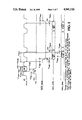
- FIG. 10 is a logic diagram of a weak/strong bus driver of the instant invention.
- bus drivers 50 and 52 are illustrated, each being on different circuits, driving the same external line 54.
- the bus drivers are programmed to drive the line 54 at different times; when they do not drive the line, they assume a "tri-state" mode as is well known to those skilled in the art.
- one driver is disabled and the other is enabled so that one driver turns off, i.e., enters the "tri-state” mode while the other turns on, i.e., begins transmitting.
- This arrangement requires that the first driver is off when the second driver turns on.
- Table I Given the spread in device characteristics of the circuit fabrication process (Table I), it is possible that the second driver 52 will turn on before the first 50 is off. As described above in connection with FIG. 4, this causes surges of current and possible circuit damage if the drivers try to set the external line at opposite levels. This problem exists because of a restriction of the circuit specifications to use only one clock edge for synchronization.
- the data rate on the serial bus 54 is dictated by PCLK.
- one driver 50 drives during a time t1 and the other 52, during a time t2.
- the drivers are otherwise in high impedance (HI-Z) state. It takes the time t3 for the first driver 50 to react to the disabling signal which puts it in high impedance mode and it takes a time t4 for the second driver 52 to react to the enabling signal which puts it in driving mode.
- the time at which either enabling or disabling signals are latched corrsponds to the falling edge of PCLK.
- t3 can be larger than t4 or conversely. We consider the case where t4 is smaller than t3. This implies that the second driver 52 is trying to drive the data on the bus 54 while the first driver 50 is still driving the bus and not yet disabled.
- the first circuit 50 is driving the bus 54 during the time t1 with a strong driver and holding the bus during a time t2 with a weak driver.
- the second circuit is driving the bus during the time t3 with a strong driver and holding the bus during a time t4 with a weak driver. It takes a time t5 for the first circuit 50 to go back to high impedance mode, and it takes a time t6 for the second circuit 52 to be enabled.
- the circuit is transmitting a series of 3 bits 56, then a series of 4 bits 58 with a "dead time" 57 in between. During that "dead time” another driver circuit can transmit data. Whatever the state of the external line is, the strong driver has to drive the first bit of each series.
- the weak/strong driver combination 60 of the instant invention is shown in FIG. 10.
- FIG. 10 indicates which portions of the device 60 are related to the strong driver 62, the weak driver 64, the sensor 66 and the first bit detection 68.
- the strong driver 62 must be used to transmit the first bit of a series, as detected by first bit detection unit 68.
- the sensor 66 detects the level of the external line 70.
- the weak driver 64 stays enabled. Otherwise, if the level of the external line is different from the one of the data to be transmitted, the strong driver 62 is enabled. As soon as the line has reached the appropriate level, the strong driver is disabled and the weak driver takes over. Therefore, whether the strong driver is enabled or not depends on the result of the comparison between what is on the line and what has to be driven on it, as determined by sensor 66.
- Control logic portions of driver 60, one 72 for the strong driver 62 and one 74 for the weak driver 64 are also shown in FIG. 10.
- the strong and weak drivers 62 and 64 each comprise two CMOS transistors 76 and 78, and 80 and 82, respectively, and two inverters 84 and 86, and 88 and 90, respectively.
- the output terminal of each inverter 84, 86, 88, 90 is connected to the gate of a corresponding transistor 76, 78, 80, 82.
- the drains of transistors 76 and 78 are connected in common and to the external line 70, as are the drains of transistors 80 and 82.
- the source of transistors 76 and 80 are connected to a positive voltage source, the drains of transistors 78 and 82 are connected to ground.
- portions 62 and 64 of driver 60 are conventional tri-state drivers.
- control logic portions 72 and 74 are conventional, each having a NOR gate 92 and 94, respectively, each having its output terminal connected to the input terminal of inverter 84 and 88, respectively. Each has a NAND gate 96 and 98, respectively, its output terminal connected to the input terminal of inverter 86 and 90, respectively.
- control logic 72 the output of a second NOR gate 100 is connected to a first input of gate 92.
- control logic 74 the output of a second NOR gate 102 is connected to a first input of gate 98.
- control logic 72 the output of a second NAND gate 104 is connected to a first input of gate 96.
- control logic 74 the output of a second NAND gate 106 is connected to a first input of gate 94.
- the data to be transmitted (DIN) in inverted form is received on signal line 72 and conducted to a second input of gates 92, 96, 94 and 98.
- a high-impedance (HIZ) input signal (active in a logic HIGH level) is received on a signal line 108 and is conducted to an input of an inverter 110.
- the HIZ signal indicates whether DIN is to be transmitted or ignored, depending on whether HIZ is active or inactive, respectively.
- the output signal generated by inverter 110 is conducted to a third input of gates 92 and 94.
- the output signal is also conducted to the input of an inverter 112 and the output signal so generated is conducted to a third input of gates 96 and 98.
- the first-bit detection 68 also receives the HIZ signal at an input to an inverter 114.
- the output signal generated by inverter 114 is conducted to an input terminal of an MOS transmission gate switch 116.
- Switch 116 receives the PCM clock (PCLK) signal which enables (closes) the switch and receives complemented PCM clock (PCLKL) which disables (opens) the switch.
- PCLK PCM clock
- PCLKL PCM clock
- the signal conducted by switch 116 is received by an inverter 118 which generates a signal conducted to an input terminal of an MOS transmission gate switch 120.
- Switch 120 receives a PCM clock fall (PCLKF) (the PCLKF signal is non-overlapping the PCLK signal) signal which disables the switch. And a complemented PCLKFL signal which disables switch 120.
- PCLKF PCM clock fall
- PCLK and PCLKF have durations as non-overlapping clocks.
- the signal conducted by switch 120 is received by an inverter 122 which generates a signal conducted to a first terminal of a NAND gate 124.
- the HIZ signal is conducted to a second terminal of NAND gate 124.
- Elements 114, 116, 118, 120, 122 and 124 form an edge detector, inverters 114 and 118 isolate stages formed by transfer gates 116 and 120, and create a storage node for the transfer gates. These elements detect the rising edge of the HIZ signal as it is first activated, indicating the first bit to be transmitted.
- the signal generated by NAND gate 124 is one PCLK period long and is active during the PCLK period corresponding to reception of the DIN signal representing the first bit to be transmitted.
- the signal generated by gate 124 is at a logic LOW level when the first bit is transmitted. This signal is conducted to a second input of gate 104 and gate 106 and via an inverter 126 to a second input of gate 100 and 102.
- sensor 66 receives the data out (DOUT) signal generated by driver 60 at the gates of a group of four CMOS transistors 128, 130, 132 and 134.
- These transistors and MOS transistors 136 and 138 form a Schmidt trigger circuit forming part of a comparator for the DIN and DOUT signals.
- the source of transistor 128 is connected to a positive voltage and the drain and source of transistors 128 and 130, respectively, are connected to the drain of transistor 136.
- the source of transistor 136 is also connected to ground.
- the gates of transistors 136 and 138 are connected to the drains of transistors 130 and 132.
- the source and drain of transistors 132 and 134, respectively, are connected to the drain of transistor 138.
- the source of transistor 138 is connected to a positive voltage and the source of transistor 134 is connected to ground.
- the common connection of gates of transistors 136 and 138, the drain of transistor 130 and source of transistor 132 is connected to an input of an inverter 140.
- the signal generated at the output of inverter 140 is conducted to a second input of gates 102 and 106, and via an inverter 142 to a second input of gates 100 and 104.
- the application of the output signal generated by first-bit detection 68 to the first terminal of gates 100, 102, 104 and 106 assures that the strong driver 62 is always enabled for transmission of the first bit of a series of bits, as described hereinabove.
- the sensor 66 operates as a Schmidt trigger that interprets a logic "1" level on line 70 as any voltage above 2.4 volts and a logic “0" as any voltage below 0.4 volts. Between these voltages, sensor 66 does not toggle. If the PCM highway line 70 is initially between these voltages, the sensor 66 does not provide the control logic portions 72 and 74 with any information about the status of the PCM highway. Accordingly, the control logic portion 72 will always cause the strong driver 62 to become enabled initially. Following the first bit of transmission, switching between the drivers occurs when sensor 66 detects a transition.
- strong driver 62 and weak driver 64 are otherwise conventional as are their control logic circuits 72 and 74, respectively. Accordingly, their operation will not be described herein.
Abstract
Description
              TABLE I
______________________________________
PCM Highway Timing
Conditions: O < Ta < 70° C., 4.75 v < Vcc <5.25 v, load
capacitance on logic outputs (Cl) = 150 pF, 360 ohm
pullup on TSCx.
Symbol Description   Min    Type Max     Unit
______________________________________
t.sub.PCY
       PCM Clock Period
                     0.122       16      us
t.sub.PCH
       PCM Clock High
                     48                  ns
       Pulse Width
t.sub.PCL
       PCM Clock Low 48                  ns
       Pulse Width
t.sub.PCF
       Fall Time of Clock
                      5          15      ns
t.sub.PCR
       Rise Time of Clock
                      5          15      ns
t.sub.FSS
       Frame Sync Setup
                     25          t.sub.PCY.sup.-30
                                         ns
       Time
t.sub.FSH
       Frame Sync Hold
                     20                  ns
       Time
t.sub.TSD
       Delay to TSC Valid
                     10          70      ns
t.sub.TSD
       Delay to TSC Off
                     10          60      ns
t.sub.DXD
       PCM Data Output
                     10          70      ns
       Delay
t.sub.DXH
       PCM Data Output
                     10          70      ns
       Hold Time
t.sub.PXZ
       PCM Data Output
                     10          70      ns
       Delay to High Z
t.sub.DRB
       PCM Data Input
                     25                  ns
       Setup Time
T.sub.DRH
       PCM Data Input
                      5                  ns
       Hold Time
______________________________________
Claims (5)
Priority Applications (4)
| Application Number | Priority Date | Filing Date | Title |
|---|---|---|---|
| US07/077,349 US4941126A (en) | 1987-07-24 | 1987-07-24 | Weak/strong bus driver |
| DE3852349T DE3852349T2 (en) | 1987-07-24 | 1988-07-05 | Weak / strong bus driver. |
| EP88110700A EP0300263B1 (en) | 1987-07-24 | 1988-07-05 | Weak/strong bus driver |
| JP63182776A JPH0771091B2 (en) | 1987-07-24 | 1988-07-21 | Bus drive circuit |
Applications Claiming Priority (1)
| Application Number | Priority Date | Filing Date | Title |
|---|---|---|---|
| US07/077,349 US4941126A (en) | 1987-07-24 | 1987-07-24 | Weak/strong bus driver |
Publications (1)
| Publication Number | Publication Date |
|---|---|
| US4941126A true US4941126A (en) | 1990-07-10 |
Family
ID=22137548
Family Applications (1)
| Application Number | Title | Priority Date | Filing Date |
|---|---|---|---|
| US07/077,349 Expired - Lifetime US4941126A (en) | 1987-07-24 | 1987-07-24 | Weak/strong bus driver |
Country Status (4)
| Country | Link |
|---|---|
| US (1) | US4941126A (en) |
| EP (1) | EP0300263B1 (en) |
| JP (1) | JPH0771091B2 (en) |
| DE (1) | DE3852349T2 (en) |
Cited By (10)
| Publication number | Priority date | Publication date | Assignee | Title |
|---|---|---|---|---|
| US5305443A (en) * | 1991-03-13 | 1994-04-19 | At&T Bell Laboratories | Microprocessor with low power bus |
| US5418935A (en) * | 1990-04-30 | 1995-05-23 | Unisys Corporation | Apparatus for preventing double drive occurrences on a common bus by delaying enablement of one driver after indication of disablement to other driver is received |
| US5729547A (en) * | 1996-02-07 | 1998-03-17 | Dutec, Inc. | Automatic driver/receiver control for half-duplex serial networks |
| US5835535A (en) * | 1992-11-23 | 1998-11-10 | Motorola, Inc. | Data bus interface apparatus which measures voltage potential on the uplink line of the data bus and removes an AC component |
| US5941997A (en) * | 1996-11-26 | 1999-08-24 | Play Incorporated | Current-based contention detection and handling system |
| US20040215856A1 (en) * | 2003-04-28 | 2004-10-28 | Yves Leduc | Terminal management bus |
| US20050213394A1 (en) * | 2004-03-24 | 2005-09-29 | Toshimasa Namekawa | Multiple-select multiplexer circuit, semiconductor memory device including a multiplexer circuit and method of testing the semiconductor memory device |
| US20080123730A1 (en) * | 2006-10-17 | 2008-05-29 | Monolithic Power Systems, Inc. | System and method for implementing a single-wire serial protocol |
| CN101165675B (en) * | 2006-10-17 | 2012-09-12 | 成都芯源系统有限公司 | System and method for implementing single serial protocol |
| CN104145256A (en) * | 2012-03-05 | 2014-11-12 | Abb技术有限公司 | Collision detection in eia-485 bus systems |
Citations (6)
| Publication number | Priority date | Publication date | Assignee | Title |
|---|---|---|---|---|
| US4242738A (en) * | 1979-10-01 | 1980-12-30 | Rca Corporation | Look ahead high speed circuitry |
| US4477741A (en) * | 1982-03-29 | 1984-10-16 | International Business Machines Corporation | Dynamic output impedance for 3-state drivers |
| US4500988A (en) * | 1982-03-08 | 1985-02-19 | Sperry Corporation | VLSI Wired-OR driver/receiver circuit |
| US4531068A (en) * | 1983-09-19 | 1985-07-23 | International Business Machines Corporation | Bus line precharging tristate driver circuit |
| US4620310A (en) * | 1985-03-11 | 1986-10-28 | Metapath Inc. | Method and apparatus for generating bipolar pulses in a local area network |
| US4734909A (en) * | 1982-03-08 | 1988-03-29 | Sperry Corporation | Versatile interconnection bus |
Family Cites Families (5)
| Publication number | Priority date | Publication date | Assignee | Title |
|---|---|---|---|---|
| US3749936A (en) * | 1971-08-19 | 1973-07-31 | Texas Instruments Inc | Fault protected output buffer |
| US4178620A (en) * | 1977-10-11 | 1979-12-11 | Signetics Corporation | Three state bus driver with protection circuitry |
| US4305106A (en) * | 1980-01-18 | 1981-12-08 | Harris Corporation | System for short circuit protection using electronic logic in a feedback arrangement |
| JPS6064547A (en) * | 1983-09-19 | 1985-04-13 | Fujitsu Ltd | Two-way signal transmission system |
| JPS6132162A (en) * | 1984-07-24 | 1986-02-14 | Fuji Photo Film Co Ltd | Competition preventing circuit of information transfer |
-
1987
- 1987-07-24 US US07/077,349 patent/US4941126A/en not_active Expired - Lifetime
-
1988
- 1988-07-05 DE DE3852349T patent/DE3852349T2/en not_active Expired - Fee Related
- 1988-07-05 EP EP88110700A patent/EP0300263B1/en not_active Expired - Lifetime
- 1988-07-21 JP JP63182776A patent/JPH0771091B2/en not_active Expired - Lifetime
Patent Citations (6)
| Publication number | Priority date | Publication date | Assignee | Title |
|---|---|---|---|---|
| US4242738A (en) * | 1979-10-01 | 1980-12-30 | Rca Corporation | Look ahead high speed circuitry |
| US4500988A (en) * | 1982-03-08 | 1985-02-19 | Sperry Corporation | VLSI Wired-OR driver/receiver circuit |
| US4734909A (en) * | 1982-03-08 | 1988-03-29 | Sperry Corporation | Versatile interconnection bus |
| US4477741A (en) * | 1982-03-29 | 1984-10-16 | International Business Machines Corporation | Dynamic output impedance for 3-state drivers |
| US4531068A (en) * | 1983-09-19 | 1985-07-23 | International Business Machines Corporation | Bus line precharging tristate driver circuit |
| US4620310A (en) * | 1985-03-11 | 1986-10-28 | Metapath Inc. | Method and apparatus for generating bipolar pulses in a local area network |
Cited By (15)
| Publication number | Priority date | Publication date | Assignee | Title |
|---|---|---|---|---|
| US5418935A (en) * | 1990-04-30 | 1995-05-23 | Unisys Corporation | Apparatus for preventing double drive occurrences on a common bus by delaying enablement of one driver after indication of disablement to other driver is received |
| US5305443A (en) * | 1991-03-13 | 1994-04-19 | At&T Bell Laboratories | Microprocessor with low power bus |
| US5835535A (en) * | 1992-11-23 | 1998-11-10 | Motorola, Inc. | Data bus interface apparatus which measures voltage potential on the uplink line of the data bus and removes an AC component |
| US5729547A (en) * | 1996-02-07 | 1998-03-17 | Dutec, Inc. | Automatic driver/receiver control for half-duplex serial networks |
| US5941997A (en) * | 1996-11-26 | 1999-08-24 | Play Incorporated | Current-based contention detection and handling system |
| US20040215856A1 (en) * | 2003-04-28 | 2004-10-28 | Yves Leduc | Terminal management bus |
| US20050213394A1 (en) * | 2004-03-24 | 2005-09-29 | Toshimasa Namekawa | Multiple-select multiplexer circuit, semiconductor memory device including a multiplexer circuit and method of testing the semiconductor memory device |
| US7064571B2 (en) | 2004-03-24 | 2006-06-20 | Kabushiki Kaisha Toshiba | Multiple-select multiplexer circuit, semiconductor memory device including a multiplexer circuit and method of testing the semiconductor memory device |
| US20080123730A1 (en) * | 2006-10-17 | 2008-05-29 | Monolithic Power Systems, Inc. | System and method for implementing a single-wire serial protocol |
| US7944807B2 (en) * | 2006-10-17 | 2011-05-17 | Monolithic Power Systems, Inc. | System and method for implementing a single-wire serial protocol |
| CN101165675B (en) * | 2006-10-17 | 2012-09-12 | 成都芯源系统有限公司 | System and method for implementing single serial protocol |
| TWI459207B (en) * | 2006-10-17 | 2014-11-01 | Monolithic Power Systems Inc | System and method for implementing a single-wire serial protocol |
| CN104145256A (en) * | 2012-03-05 | 2014-11-12 | Abb技术有限公司 | Collision detection in eia-485 bus systems |
| US20140372645A1 (en) * | 2012-03-05 | 2014-12-18 | Abb Technology Ag | Collision detection in eia-485 bus systems |
| US9678919B2 (en) * | 2012-03-05 | 2017-06-13 | Abb Schweiz Ag | Collision detection in EIA-485 bus systems |
Also Published As
| Publication number | Publication date |
|---|---|
| JPS6444144A (en) | 1989-02-16 |
| DE3852349T2 (en) | 1995-07-27 |
| EP0300263A2 (en) | 1989-01-25 |
| JPH0771091B2 (en) | 1995-07-31 |
| DE3852349D1 (en) | 1995-01-19 |
| EP0300263B1 (en) | 1994-12-07 |
| EP0300263A3 (en) | 1991-11-06 |
Similar Documents
| Publication | Publication Date | Title |
|---|---|---|
| US5455802A (en) | Dual dynamic sense amplifiers for a memory array | |
| KR0164807B1 (en) | Data output buffer control circuit for semiconductor memory device | |
| EP0647028B1 (en) | Latch controlled output driver | |
| US4941126A (en) | Weak/strong bus driver | |
| KR100506063B1 (en) | Apparatus for controlling setup/hold time | |
| KR100223675B1 (en) | Data-output-related circuit suitable for high speed semiconductor memory device | |
| WO1986001658A1 (en) | Assist circuit for improving the rise time of an electronic signal | |
| US7982505B2 (en) | Logic circuit, address decoder circuit and semiconductor memory | |
| KR100789195B1 (en) | Input/output interface and semiconductor integrated circuit having input/output interface | |
| US4808855A (en) | Distributed precharge wire-or bus | |
| US7365587B2 (en) | Contention-free keeper circuit and a method for contention elimination | |
| KR19990081109A (en) | Phase separator | |
| US6411553B1 (en) | Single ended data bus equilibration scheme | |
| US8432195B2 (en) | Latch circuits with synchronous data loading and self-timed asynchronous data capture | |
| EP0777328A2 (en) | Bus driver failure detection systems | |
| US5469476A (en) | Circuit and method for filtering voltage spikes | |
| EP0808022B1 (en) | Latch circuit operating in synchronization with clock signals | |
| KR100316184B1 (en) | Auto-precharge controller | |
| KR100323642B1 (en) | Improved clock-synchronizing semiconductor memory device | |
| US5905678A (en) | Control circuit of an output buffer | |
| EP0678870B1 (en) | Method and circuit for suppressing data loading noise in non-volatile memories | |
| KR100293730B1 (en) | Data output buffer | |
| US5970014A (en) | Semiconductor memory device having two or more memory blocks | |
| KR100508722B1 (en) | Apparutus for fixing pulse width | |
| EP0915477B1 (en) | Method and circuit for generating an ATD signal to regulate the access to a non-volatile memory |
Legal Events
| Date | Code | Title | Description |
|---|---|---|---|
| AS | Assignment |
Owner name: ADVANCED MICRO DEVICES, INC., 901 THOMPSON PLACE, Free format text: ASSIGNMENT OF ASSIGNORS INTEREST.;ASSIGNOR:HAUBURSIN, PIERRE F.;REEL/FRAME:004749/0829 Effective date: 19870709 |
|
| FEPP | Fee payment procedure |
Free format text: PAYOR NUMBER ASSIGNED (ORIGINAL EVENT CODE: ASPN); ENTITY STATUS OF PATENT OWNER: LARGE ENTITY |
|
| STCF | Information on status: patent grant |
Free format text: PATENTED CASE |
|
| FPAY | Fee payment |
Year of fee payment: 4 |
|
| SULP | Surcharge for late payment | ||
| FPAY | Fee payment |
Year of fee payment: 8 |
|
| AS | Assignment |
Owner name: MORGAN STANLEY & CO. INCORPORATED, NEW YORK Free format text: SECURITY INTEREST;ASSIGNOR:LEGERITY, INC.;REEL/FRAME:011601/0539 Effective date: 20000804 |
|
| AS | Assignment |
Owner name: LEGERITY, INC., TEXAS Free format text: ASSIGNMENT OF ASSIGNORS INTEREST;ASSIGNOR:ADVANCED MICRO DEVICES, INC.;REEL/FRAME:011700/0686 Effective date: 20000731 |
|
| FPAY | Fee payment |
Year of fee payment: 12 |
|
| AS | Assignment |
Owner name: MORGAN STANLEY & CO. INCORPORATED, AS FACILITY COL Free format text: SECURITY AGREEMENT;ASSIGNORS:LEGERITY, INC.;LEGERITY HOLDINGS, INC.;LEGERITY INTERNATIONAL, INC.;REEL/FRAME:013372/0063 Effective date: 20020930 |
|
| AS | Assignment |
Owner name: LEGERITY, INC., TEXAS Free format text: RELEASE BY SECURED PARTY;ASSIGNOR:MORGAN STANLEY SENIOR FUNDING INC;REEL/FRAME:019640/0676 Effective date: 20070803 Owner name: LEGERITY, INC.,TEXAS Free format text: RELEASE BY SECURED PARTY;ASSIGNOR:MORGAN STANLEY SENIOR FUNDING INC;REEL/FRAME:019640/0676 Effective date: 20070803 |