US5122848A - Insulated-gate vertical field-effect transistor with high current drive and minimum overlap capacitance - Google Patents
Insulated-gate vertical field-effect transistor with high current drive and minimum overlap capacitance Download PDFInfo
- Publication number
- US5122848A US5122848A US07/682,623 US68262391A US5122848A US 5122848 A US5122848 A US 5122848A US 68262391 A US68262391 A US 68262391A US 5122848 A US5122848 A US 5122848A
- Authority
- US
- United States
- Prior art keywords
- layer
- trench
- gate
- effect transistor
- vertical field
- Prior art date
- Legal status (The legal status is an assumption and is not a legal conclusion. Google has not performed a legal analysis and makes no representation as to the accuracy of the status listed.)
- Expired - Lifetime
Links
- 230000005669 field effect Effects 0.000 title claims description 19
- 229910021420 polycrystalline silicon Inorganic materials 0.000 claims abstract description 36
- 229920005591 polysilicon Polymers 0.000 claims abstract description 36
- 125000006850 spacer group Chemical group 0.000 claims abstract description 24
- 239000000758 substrate Substances 0.000 claims abstract description 19
- 239000004065 semiconductor Substances 0.000 claims abstract description 8
- 230000003071 parasitic effect Effects 0.000 claims description 10
- 239000004020 conductor Substances 0.000 claims 1
- 239000007943 implant Substances 0.000 abstract description 5
- XUIMIQQOPSSXEZ-UHFFFAOYSA-N Silicon Chemical compound [Si] XUIMIQQOPSSXEZ-UHFFFAOYSA-N 0.000 description 7
- 229910052710 silicon Inorganic materials 0.000 description 7
- 239000010703 silicon Substances 0.000 description 7
- 150000002500 ions Chemical class 0.000 description 6
- 239000000463 material Substances 0.000 description 4
- 238000004519 manufacturing process Methods 0.000 description 3
- 229920002120 photoresistant polymer Polymers 0.000 description 3
- 239000003990 capacitor Substances 0.000 description 2
- 230000015556 catabolic process Effects 0.000 description 2
- 239000002019 doping agent Substances 0.000 description 2
- BHEPBYXIRTUNPN-UHFFFAOYSA-N hydridophosphorus(.) (triplet) Chemical compound [PH] BHEPBYXIRTUNPN-UHFFFAOYSA-N 0.000 description 2
- 230000010354 integration Effects 0.000 description 2
- 230000000873 masking effect Effects 0.000 description 2
- 229910052782 aluminium Inorganic materials 0.000 description 1
- XAGFODPZIPBFFR-UHFFFAOYSA-N aluminium Chemical compound [Al] XAGFODPZIPBFFR-UHFFFAOYSA-N 0.000 description 1
- 230000003247 decreasing effect Effects 0.000 description 1
- PCHJSUWPFVWCPO-UHFFFAOYSA-N gold Chemical compound [Au] PCHJSUWPFVWCPO-UHFFFAOYSA-N 0.000 description 1
- 229910052737 gold Inorganic materials 0.000 description 1
- 239000010931 gold Substances 0.000 description 1
- 229910052751 metal Inorganic materials 0.000 description 1
- 239000002184 metal Substances 0.000 description 1
- 238000000034 method Methods 0.000 description 1
- 238000012986 modification Methods 0.000 description 1
- 230000004048 modification Effects 0.000 description 1
- 239000007858 starting material Substances 0.000 description 1
Images


Classifications
-
- H—ELECTRICITY
- H10—SEMICONDUCTOR DEVICES; ELECTRIC SOLID-STATE DEVICES NOT OTHERWISE PROVIDED FOR
- H10B—ELECTRONIC MEMORY DEVICES
- H10B12/00—Dynamic random access memory [DRAM] devices
- H10B12/01—Manufacture or treatment
- H10B12/02—Manufacture or treatment for one transistor one-capacitor [1T-1C] memory cells
- H10B12/03—Making the capacitor or connections thereto
- H10B12/038—Making the capacitor or connections thereto the capacitor being in a trench in the substrate
- H10B12/0383—Making the capacitor or connections thereto the capacitor being in a trench in the substrate wherein the transistor is vertical
-
- H—ELECTRICITY
- H01—ELECTRIC ELEMENTS
- H01L—SEMICONDUCTOR DEVICES NOT COVERED BY CLASS H10
- H01L29/00—Semiconductor devices adapted for rectifying, amplifying, oscillating or switching, or capacitors or resistors with at least one potential-jump barrier or surface barrier, e.g. PN junction depletion layer or carrier concentration layer; Details of semiconductor bodies or of electrodes thereof ; Multistep manufacturing processes therefor
- H01L29/66—Types of semiconductor device ; Multistep manufacturing processes therefor
- H01L29/66007—Multistep manufacturing processes
- H01L29/66075—Multistep manufacturing processes of devices having semiconductor bodies comprising group 14 or group 13/15 materials
- H01L29/66227—Multistep manufacturing processes of devices having semiconductor bodies comprising group 14 or group 13/15 materials the devices being controllable only by the electric current supplied or the electric potential applied, to an electrode which does not carry the current to be rectified, amplified or switched, e.g. three-terminal devices
- H01L29/66409—Unipolar field-effect transistors
- H01L29/66477—Unipolar field-effect transistors with an insulated gate, i.e. MISFET
- H01L29/66666—Vertical transistors
-
- H—ELECTRICITY
- H01—ELECTRIC ELEMENTS
- H01L—SEMICONDUCTOR DEVICES NOT COVERED BY CLASS H10
- H01L29/00—Semiconductor devices adapted for rectifying, amplifying, oscillating or switching, or capacitors or resistors with at least one potential-jump barrier or surface barrier, e.g. PN junction depletion layer or carrier concentration layer; Details of semiconductor bodies or of electrodes thereof ; Multistep manufacturing processes therefor
- H01L29/66—Types of semiconductor device ; Multistep manufacturing processes therefor
- H01L29/68—Types of semiconductor device ; Multistep manufacturing processes therefor controllable by only the electric current supplied, or only the electric potential applied, to an electrode which does not carry the current to be rectified, amplified or switched
- H01L29/76—Unipolar devices, e.g. field effect transistors
- H01L29/772—Field effect transistors
- H01L29/78—Field effect transistors with field effect produced by an insulated gate
- H01L29/7827—Vertical transistors
Definitions
- This invention relates generally to field-effect transistors ("FETs”), and more particularly to those FETs having a channel region that is generally vertical with respect to the horizontal plane of the silicon wafer.
- the area of an individual transistor on the integrated circuit must decrease in order to maintain die size and to control manufacturing costs.
- vertical FETs were introduced either in a trench or a V-groove to align the channel region of the FET vertically. Therefore, the area of the FET could be reduced because the channel did not use valuable horizontal area leading to a larger die area.
- a problem with many of the vertical designs is that performance is sacrificed as the area is decreased.
- Parasitic capacitance from the gate of the FET to the source (“overlap capacitance"), drain, or substrate can increase in the vertical FET, which results in a lower maximum operating frequency.
- the drain contact is made at the bottom of the FET through the substrate or by directly metallizing the bottom surface of the die, and thus the drain and source contacts cannot both be made at the surface of the transistor.
- a need remains for a vertical FET having an area smaller than a horizontal FET having a comparable channel region, while having minimum gate parasitic capacitance and the option of surface gate, source, and drain contacts.
- an object of the invention to provide a vertical FET having a small horizontal area suitable for high density integration on a silicon die.
- Another object of the invention is to provide a vertical FET having low parasitic gate capacitance in order to maintain a high maximum operating frequency.
- a further object of the invention is to provide a vertical FET having a high current drive capability.
- An advantage of the invention is that the vertical FET requires no additional masking steps beyond those normally required for the fabrication of an integrated random access memory.
- Another advantage of the invention is that the source, drain, and gate contacts of the vertical FET may all be contacted from the top surface of the die, if desired.
- Another advantage of the invention is that the gate region within each trench sidewall contains no discontinuous features that decrease breakdown voltage.
- an insulatedgate vertical FET has a channel region and gate structure that is formed along the sidewall of trench in a P-type semiconductor substrate.
- the drain and source regions of the FET are formed in the mesa and the base portions of the trench. All contacts to the gate, drain, and source regions can be made from the top surface of the semiconductor substrate.
- One or more sidewalls of the trench are oxidized with a thin gate oxide dielectric layer followed by a thin polysilicon deposited film to form an insulated gate layer.
- a reactive ion etch step removes the insulated gate layer from the mesa and the base portions of the trench.
- An enhanced N-type implant creates the drain and source regions in the mesa and the base portions of the trench.
- the trench is partially filled with a spacer oxide layer to reduce gate-to-source overlap capacitance.
- a conformal conductive polysilicon layer is deposited over the insulated gate layer.
- a portion of the conductive polysilicon layer is extended above the surface of the trench onto the mesa to form a gate contact.
- a field oxide covers the entire surface of the FET, which is opened in the mesa to form gate and drain contacts, and in the base to form the source contact.
- FIGS. 1-1A, 2-3, 4-4A, 5, 6-6A, 7, 8 and 8A are plan and sectional views of a semiconductor substrate at various stages of processing in accordance with the invention that ultimately form an insulated-gate vertical FET.
- a semiconductor substrate 12 forms the starting material for the FET.
- the substrate material can be P-type or N-type silicon formed in a wafer, epitaxial layer, or well.
- the top surface of the substrate defines a reference surface for defining subsequent vertical structures.
- a trench in the substrate 12 forms the channel region and the gate structure of the vertical FET 10.
- the trench defines a surface including first and second mesa portions 14A and 14B at the level of the reference surface of the substrate 12, one or more sidewalls 16, and a base 18 recessed from the reference surface.
- An insulated gate layer 20 is formed on the sidewalls 16 of the trench, which includes a gate dielectric layer 22 and a gate conductive layer 24.
- a first enhanced N-type layer 26 implanted in the first portion of the mesa l4A forms the first current node of the transistor, typically the drain. However, since the drain and source are interchangeable in an FET, the N-type layer 26 can also serve as the source.
- a second enhanced N-type layer 28 is implanted in the base 18 of the trench to form the second current node of the transistor, typically the source. Again, given the interchangeability of the current nodes, the second enhanced N-type layer 28 can also serve as the drain.
- a spacer dielectric layer 30 partially fills the base 18 of the trench and a conductive layer 32 is deposited along the sidewalls 16 of the trench over the insulated gate layer 20 extending from the spacer dielectric layer 30 to the reference surface of the substrate 12.
- the conductive layer 32 forms part of a gate contact and is spaced apart from the enhanced N-type layer 28 by the spacer dielectric layer 30 to decrease the parasitic overlap capacitance between the gate and source of the FET.
- the conductive layer 32 and the spacer dielectric layer 30 are opened to expose the second enhanced N-type layer 28.
- a field dielectric layer 34 covers the entire surface of the FET 10, and is opened in three places to form drain, source, and gate contacts.
- the field dielectric layer 34 is opened above the first enhanced N-type layer 26 to form a drain contact 36, which is covered with an interconnect line 42; above the second enhanced N-type layer 28 to form a source contact 38, which is covered with an interconnect line 44; and above the conductive layer 32 in the second portion 14B of the mesa to form a gate contact 40, which is covered with an interconnect line 46.
- FIG. 1 there is shown a sectional view of a partially processed silicon substrate 12 having a patterned photoresist layer 11 over an optional thin grown oxide layer 15.
- the substrate can be either P-type or N-type material depending upon whether an N-channel or a P-channel FET is desired.
- FIG. 1A is a corresponding plan view showing the contours of the photoresist opening, which will determine the nature of the trench. In the case of a rectangular pattern, a trench having four sidewalls and a rectangular base is formed. Other patterns, including a circular pattern resulting in one continuous sidewall and polygonal patterns resulting in multiple sidewalls are possible within the constraints of the photolithographic equipment that is used.
- the trench is formed with a reactive ion etch, revealing first and second mesa portions 14A and 14B, sidewalls 16, and a base portion 18.
- the sidewalls 16 of the trench form the body of the FET 10 that includes the channel region.
- the FET 10 can thus be formed in one or more of the sidewalls 16.
- the etchant species for removing the silicon substrate and creating the trench can be CF 4 , or any other conventional etchant species.
- the depth of the trench defines the length of the channel of the FET 10. Therefore, the channel is ideally etched to a depth equal to the desired length of the channel region, up to a maximum length of about 8000 to 10000 Angstroms.
- the width, and consequently the width to length (“W/L”) ratio of the FET 10, is determined by the dimensions of the photoresist pattern.
- the insulated gate layer 20 is revealed in greater detail.
- the insulated gate layer 20 is comprised of a gate dielectric layer 22 such as oxide, and a gate conductive layer 24 such as polysilicon.
- the gate oxide layer is grown along the entire surface of the trench to a depth of about 200 to 250 Angstroms, but this depth can be made thinner or thicker as required by the application.
- the thin gate polysilicon layer 24 is deposited onto the surface of the oxide layer 22 to a thickness of about 500 to 1000 Angstroms. Again, the thickness can be easily adjusted as required by the application.
- the gate polysilicon layer 24 is highly conformal with oxide layer 22.
- the gate polysilicon layer 24 forms the active gate contact of the FET 10, which inverts the substrate silicon 12 in the sidewalls 16 of the trench.
- the gate polysilicon layer 24 be doped with an appropriate dopant such as phosphorous to form a conductive layer capable of inverting the entire channel region.
- a suitable sheet resistance for the gate polysilicon layer 24 after the doping step is completed is about 50 ohms per square.
- the insulated gate layer 24 is removed in a first portion l4A of the mesa, and first and second enhanced N-type ("N+") layers 26 and 28 are implanted into the first portion l4A of the mesa and into the base of the trench 18 to form the active drain and source of the FET 10.
- the gate polysilicon layer 24 is removed with a reactive ion etch.
- the gate polysilicon layer remains on the sidewalls 16 since the reactive ion etch acts primarily in the vertical directional and the gate polysilicon layer 24 is conformal to the sidewalls 16.
- the gate oxide layer 22 is removed from the first portion 14A of the mesa and the base 18 by an oxide etch.
- first and second enhanced N-type layers 26 and 28 are implanted into the first portion of the mesa 14A and the base 18.
- a suitable implant dosage is 9 ⁇ 10 15 ions per cm 2 at 30 KeV.
- the P-N junction between the enhanced N-type layers and the P-type body of the FET 10 using this implant dosage occurs at a depth of approximately 2000 to 4000 Angstroms.
- FIG. 4A The corresponding plan view is shown in FIG. 4A, revealing the first enhanced N-type layer 26 in the first portion of the mesa l4A, the gate dielectric layer 22 and the gate conductive layer 24 along the sidewalls of the trench and in the second portion of the mesa 14B, and the second enhanced N-type layer 28 in the base of the trench.
- the base 18 of the trench is partially filled with a spacer oxide layer 30 in FIG. 5.
- the spacer oxide layer 30 minimizes the parasitic overlap capacitance between the gate and the source of the FET 10.
- the spacer oxide layer 30 is a thick conformal layer that is deposited over the surface of the FET 10, which completely fills in the trench.
- a mechanical planerization removes most of the spacer oxide layer 30 from the mesa portions of the trench, while leaving the spacer oxide layer 30 in the trench.
- a subsequent oxide etch removes any remaining oxide from the mesa portions of the trench, and etches back the spacer oxide layer 30 in the trench to partially fill the trench to a thickness of about 2000 to 3000 Angstroms.
- the thickness of the spacer oxide layer 30 can be adjusted depending upon the reduction in the parasitic overlap capacitance that is desired.
- a conductive layer 32 is added that contacts the insulated gate layer 20 in order to provide a surface contact for the gate of the FET 10.
- the conductive layer 32 is a conformal polysilicon layer that is deposited over the entire surface. Once the conductive layer 32 has been deposited, it is masked and etched away in the first portion l4A of the mesa and at the base 18 of the trench. The conductive layer remains on the sidewalls 16 of the trench and in the second portion 14B of the mesa.
- a suitable thickness for the conductive layer is about 2000 Angstroms.
- the polysilicon is doped with an appropriate dopant such as phosphorous to render it conductive.
- a suitable sheet resistance upon completion of the doping step is about 25 to 35 ohms per square.
- FIG. 6A The corresponding plan view is shown in FIG. 6A, revealing the first enhanced N-type layer 26 in the first portion of the mesa l4A, the gate dielectric layer 22, the gate conductive layer 24, and the conductive layer 32 along the sidewalls of the trench and in the second portion of the mesa 14B, and the spacer dielectric layer 30 in the base of the trench.
- a center portion of the spacer dielectric layer 30 is etched away using a conventional oxide etch to reveal the second enhanced N-type layer 28.
- the opening in the spacer dielectric layer 30 subsequently serves as a top surface source contact.
- a thick, conformal field dielectric layer 34 such as oxide is subsequently deposited over the entire surface of the FET 10.
- the field dielectric is etched in three places to form a drain contact 36, a source contact 38, and a gate contact 40.
- Each contact is respectively covered with a separate interconnect line 42, 44, and 46 for interconnecting the FET 10 with other circuit components.
- the interconnect lines can be polysilicon, doped polysilicon, or metal such as gold or aluminum.
- FIG. 8A The corresponding plan view is shown in FIG. 8A in outline form only.
- the outline of the gate dielectric layer 22, the gate conductive layer 24, and the conductive layer 32 along the sidewalls of the trench and in the second portion of the mesa 14B is shown.
- the location of the drain contact 36, source contact 38, and gate contact 40, as well as the drain interconnect line 42, the source interconnect line 44, and the gate interconnect line is also shown.
- an insulated-gate vertical FET has a small horizontal area suitable for high density integration on a silicon die, since the gate and channel area are disposed along and within one or more sidewalls of the trench.
- the active gate region is continuous along the trench sidewall and is protected from further processing steps.
- the active gate region within each trench sidewall 16 is continuous from the mesa to the base and contains no sharp corners, edges, steps or other such discontinuous features that decrease breakdown voltage.
- Low parasitic gate-to-source overlap capacitance is reduced by the spacer dielectric layer 30 in order to maintain a high maximum operating frequency. Note in FIG. 8 that only the thin gate conductive layer 24 remains in close proximity to the second enhanced N-type layer 28, establishing a minimum overlap capacitance.
- the vertical FET has a high current drive capability at a given W/L ratio since the parasitic capacitance is low. It has also been shown that the vertical FET 10 requires no additional masking steps beyond those normally required for the fabrication of an integrated random access memory. For example, the N+ implant used to form the source and drain regions is typically creates the storage node of the capacitor for a memory cell.
- the source, drain, and gate contacts of the vertical FET 10 may all be contacted from the top surface of the die, if desired. It is appreciated, however, by those skilled in the art that the exact configuration and layout of the FET 10 can be changed in many ways. For example, the drain and gate contacts need not be placed in a row as shown in FIGS. 8 and 8A, but can be orthogonally arranged if required by layout considerations. Also, the source region of the FET 10 need not be contacted from the surface, but can be contacted through additional N-type layers in contact with N-type layer 28, or by directly metallizing the bottom surface of the die by any conventional means taught in the prior art. The source region of the FET 10 may also be coupled to a capacitor in a DRAM array configuration, while still maintaining the minimized gate-to-source overlap capacitance of the present invention.
- the vertical FET 10 of the present invention is suitable for use in many applications, such as in a DRAM array, in an inverter, a buffer or driver circuit, or a stand-alone power FET. If minimum area is required, it is desirable that the gate of the vertical FET 10 be constructed in only one of the sidewalls of a rectangular trench. If maximum drive current is required for a power FET, it is desirable that the gate of the vertical FET 10 be constructed in all four sidewalls of a rectangular trench.
Abstract
An insulated-gate vertical FET has a channel region and gate structure that is formed along the sidewall of trench in a P-type semiconductor substrate. The drain and source regions of the FET are formed in the mesa and the base portions of the trench. All contacts to the gate, drain, and source regions can be made from the top surface of the semiconductor substrate. One or more sidewalls of the trench are oxidized with a thin gate oxide dielectric layer followed by a thin polysilicon deposited film to form an insulated gate layer. A reactive ion etch step removes the insulated gate layer from the mesa and the base portion of the trench. An enhanced N-type implant creates the drain and source regions in the mesa and the base portions of the trench. The trench is partially filled with a spacer oxide layer to reduce gate-to-source overlap capacitance. A conformal conductive polysilicon layer is deposited over the insulated gate layer. A portion of the conductive polysilicon layer is extended above the surface of the trench onto the mesa to form a gate contact. A field oxide covers the entire surface of the FET, which is opened in the mesa to form gate and drain contacts, and in the base to form the source contact.
Description
This invention relates generally to field-effect transistors ("FETs"), and more particularly to those FETs having a channel region that is generally vertical with respect to the horizontal plane of the silicon wafer.
As the performance and complexity of integrated circuits, and in particular memory circuits, increases, the area of an individual transistor on the integrated circuit must decrease in order to maintain die size and to control manufacturing costs. In the past, vertical FETs were introduced either in a trench or a V-groove to align the channel region of the FET vertically. Therefore, the area of the FET could be reduced because the channel did not use valuable horizontal area leading to a larger die area. A problem with many of the vertical designs is that performance is sacrificed as the area is decreased. Parasitic capacitance from the gate of the FET to the source ("overlap capacitance"), drain, or substrate can increase in the vertical FET, which results in a lower maximum operating frequency. In addition, in many vertical designs, the drain contact is made at the bottom of the FET through the substrate or by directly metallizing the bottom surface of the die, and thus the drain and source contacts cannot both be made at the surface of the transistor.
Accordingly, a need remains for a vertical FET having an area smaller than a horizontal FET having a comparable channel region, while having minimum gate parasitic capacitance and the option of surface gate, source, and drain contacts.
It is, therefore, an object of the invention to provide a vertical FET having a small horizontal area suitable for high density integration on a silicon die.
Another object of the invention is to provide a vertical FET having low parasitic gate capacitance in order to maintain a high maximum operating frequency.
A further object of the invention is to provide a vertical FET having a high current drive capability.
An advantage of the invention is that the vertical FET requires no additional masking steps beyond those normally required for the fabrication of an integrated random access memory.
Another advantage of the invention is that the source, drain, and gate contacts of the vertical FET may all be contacted from the top surface of the die, if desired.
Another advantage of the invention is that the gate region within each trench sidewall contains no discontinuous features that decrease breakdown voltage.
According to the present invention, an insulatedgate vertical FET has a channel region and gate structure that is formed along the sidewall of trench in a P-type semiconductor substrate. The drain and source regions of the FET are formed in the mesa and the base portions of the trench. All contacts to the gate, drain, and source regions can be made from the top surface of the semiconductor substrate. One or more sidewalls of the trench are oxidized with a thin gate oxide dielectric layer followed by a thin polysilicon deposited film to form an insulated gate layer. A reactive ion etch step removes the insulated gate layer from the mesa and the base portions of the trench. An enhanced N-type implant creates the drain and source regions in the mesa and the base portions of the trench. The trench is partially filled with a spacer oxide layer to reduce gate-to-source overlap capacitance. A conformal conductive polysilicon layer is deposited over the insulated gate layer. A portion of the conductive polysilicon layer is extended above the surface of the trench onto the mesa to form a gate contact. A field oxide covers the entire surface of the FET, which is opened in the mesa to form gate and drain contacts, and in the base to form the source contact.
The foregoing and other objects, features and advantages of the invention are more readily apparent from the following detailed description of a preferred embodiment of the invention, which proceeds with reference to the accompanying drawings.
BRIEF DESCRIPTION OF THE DRAWING FIGURES
FIGS. 1-1A, 2-3, 4-4A, 5, 6-6A, 7, 8 and 8A are plan and sectional views of a semiconductor substrate at various stages of processing in accordance with the invention that ultimately form an insulated-gate vertical FET.
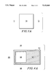
The sectional view of a completed insulated-gate vertical FET 10 is shown in the sectional view of FIG. 8. A semiconductor substrate 12 forms the starting material for the FET. The substrate material can be P-type or N-type silicon formed in a wafer, epitaxial layer, or well. The top surface of the substrate defines a reference surface for defining subsequent vertical structures. A trench in the substrate 12 forms the channel region and the gate structure of the vertical FET 10. The trench defines a surface including first and second mesa portions 14A and 14B at the level of the reference surface of the substrate 12, one or more sidewalls 16, and a base 18 recessed from the reference surface. An insulated gate layer 20 is formed on the sidewalls 16 of the trench, which includes a gate dielectric layer 22 and a gate conductive layer 24.
A first enhanced N-type layer 26 implanted in the first portion of the mesa l4A forms the first current node of the transistor, typically the drain. However, since the drain and source are interchangeable in an FET, the N-type layer 26 can also serve as the source. A second enhanced N-type layer 28 is implanted in the base 18 of the trench to form the second current node of the transistor, typically the source. Again, given the interchangeability of the current nodes, the second enhanced N-type layer 28 can also serve as the drain.
A spacer dielectric layer 30 partially fills the base 18 of the trench and a conductive layer 32 is deposited along the sidewalls 16 of the trench over the insulated gate layer 20 extending from the spacer dielectric layer 30 to the reference surface of the substrate 12. The conductive layer 32 forms part of a gate contact and is spaced apart from the enhanced N-type layer 28 by the spacer dielectric layer 30 to decrease the parasitic overlap capacitance between the gate and source of the FET.
The conductive layer 32 and the spacer dielectric layer 30 are opened to expose the second enhanced N-type layer 28. A field dielectric layer 34 covers the entire surface of the FET 10, and is opened in three places to form drain, source, and gate contacts. The field dielectric layer 34 is opened above the first enhanced N-type layer 26 to form a drain contact 36, which is covered with an interconnect line 42; above the second enhanced N-type layer 28 to form a source contact 38, which is covered with an interconnect line 44; and above the conductive layer 32 in the second portion 14B of the mesa to form a gate contact 40, which is covered with an interconnect line 46.
The structure and method for making the FET 10, and the nature of the individual layers including dimensions and suitable materials is described in greater detail below.
Referring now to FIG. 1, there is shown a sectional view of a partially processed silicon substrate 12 having a patterned photoresist layer 11 over an optional thin grown oxide layer 15. The substrate can be either P-type or N-type material depending upon whether an N-channel or a P-channel FET is desired. FIG. 1A is a corresponding plan view showing the contours of the photoresist opening, which will determine the nature of the trench. In the case of a rectangular pattern, a trench having four sidewalls and a rectangular base is formed. Other patterns, including a circular pattern resulting in one continuous sidewall and polygonal patterns resulting in multiple sidewalls are possible within the constraints of the photolithographic equipment that is used.
In FIG. 2, the trench is formed with a reactive ion etch, revealing first and second mesa portions 14A and 14B, sidewalls 16, and a base portion 18. The sidewalls 16 of the trench form the body of the FET 10 that includes the channel region. The FET 10 can thus be formed in one or more of the sidewalls 16. The etchant species for removing the silicon substrate and creating the trench can be CF4, or any other conventional etchant species. The depth of the trench defines the length of the channel of the FET 10. Therefore, the channel is ideally etched to a depth equal to the desired length of the channel region, up to a maximum length of about 8000 to 10000 Angstroms. The width, and consequently the width to length ("W/L") ratio of the FET 10, is determined by the dimensions of the photoresist pattern.
In FIG. 3, the insulated gate layer 20 is revealed in greater detail. The insulated gate layer 20 is comprised of a gate dielectric layer 22 such as oxide, and a gate conductive layer 24 such as polysilicon. The gate oxide layer is grown along the entire surface of the trench to a depth of about 200 to 250 Angstroms, but this depth can be made thinner or thicker as required by the application. The thin gate polysilicon layer 24 is deposited onto the surface of the oxide layer 22 to a thickness of about 500 to 1000 Angstroms. Again, the thickness can be easily adjusted as required by the application. The gate polysilicon layer 24 is highly conformal with oxide layer 22. The gate polysilicon layer 24 forms the active gate contact of the FET 10, which inverts the substrate silicon 12 in the sidewalls 16 of the trench. Therefore, it is desirable that the gate polysilicon layer 24 be doped with an appropriate dopant such as phosphorous to form a conductive layer capable of inverting the entire channel region. A suitable sheet resistance for the gate polysilicon layer 24 after the doping step is completed is about 50 ohms per square.
In FIG. 4, the insulated gate layer 24 is removed in a first portion l4A of the mesa, and first and second enhanced N-type ("N+") layers 26 and 28 are implanted into the first portion l4A of the mesa and into the base of the trench 18 to form the active drain and source of the FET 10. The gate polysilicon layer 24 is removed with a reactive ion etch. The gate polysilicon layer remains on the sidewalls 16 since the reactive ion etch acts primarily in the vertical directional and the gate polysilicon layer 24 is conformal to the sidewalls 16. After the gate polysilicon layer 24 is removed with the reactive ion etch, the gate oxide layer 22 is removed from the first portion 14A of the mesa and the base 18 by an oxide etch. After the insulated gate layer 20 is removed, first and second enhanced N- type layers 26 and 28 are implanted into the first portion of the mesa 14A and the base 18. A suitable implant dosage is 9×10¹⁵ ions per cm2 at 30 KeV. The P-N junction between the enhanced N-type layers and the P-type body of the FET 10 using this implant dosage occurs at a depth of approximately 2000 to 4000 Angstroms.
The corresponding plan view is shown in FIG. 4A, revealing the first enhanced N-type layer 26 in the first portion of the mesa l4A, the gate dielectric layer 22 and the gate conductive layer 24 along the sidewalls of the trench and in the second portion of the mesa 14B, and the second enhanced N-type layer 28 in the base of the trench.
The base 18 of the trench is partially filled with a spacer oxide layer 30 in FIG. 5. The spacer oxide layer 30 minimizes the parasitic overlap capacitance between the gate and the source of the FET 10. The spacer oxide layer 30 is a thick conformal layer that is deposited over the surface of the FET 10, which completely fills in the trench. A mechanical planerization removes most of the spacer oxide layer 30 from the mesa portions of the trench, while leaving the spacer oxide layer 30 in the trench. A subsequent oxide etch removes any remaining oxide from the mesa portions of the trench, and etches back the spacer oxide layer 30 in the trench to partially fill the trench to a thickness of about 2000 to 3000 Angstroms. However, the thickness of the spacer oxide layer 30 can be adjusted depending upon the reduction in the parasitic overlap capacitance that is desired.
In FIG. 6 a conductive layer 32 is added that contacts the insulated gate layer 20 in order to provide a surface contact for the gate of the FET 10. The conductive layer 32 is a conformal polysilicon layer that is deposited over the entire surface. Once the conductive layer 32 has been deposited, it is masked and etched away in the first portion l4A of the mesa and at the base 18 of the trench. The conductive layer remains on the sidewalls 16 of the trench and in the second portion 14B of the mesa. A suitable thickness for the conductive layer is about 2000 Angstroms. The polysilicon is doped with an appropriate dopant such as phosphorous to render it conductive. A suitable sheet resistance upon completion of the doping step is about 25 to 35 ohms per square.
The corresponding plan view is shown in FIG. 6A, revealing the first enhanced N-type layer 26 in the first portion of the mesa l4A, the gate dielectric layer 22, the gate conductive layer 24, and the conductive layer 32 along the sidewalls of the trench and in the second portion of the mesa 14B, and the spacer dielectric layer 30 in the base of the trench.
In FIG. 7, a center portion of the spacer dielectric layer 30 is etched away using a conventional oxide etch to reveal the second enhanced N-type layer 28. The opening in the spacer dielectric layer 30 subsequently serves as a top surface source contact. A thick, conformal field dielectric layer 34 such as oxide is subsequently deposited over the entire surface of the FET 10. As discussed above, the field dielectric is etched in three places to form a drain contact 36, a source contact 38, and a gate contact 40. Each contact is respectively covered with a separate interconnect line 42, 44, and 46 for interconnecting the FET 10 with other circuit components. The interconnect lines can be polysilicon, doped polysilicon, or metal such as gold or aluminum.
The corresponding plan view is shown in FIG. 8A in outline form only. The outline of the gate dielectric layer 22, the gate conductive layer 24, and the conductive layer 32 along the sidewalls of the trench and in the second portion of the mesa 14B is shown. The location of the drain contact 36, source contact 38, and gate contact 40, as well as the drain interconnect line 42, the source interconnect line 44, and the gate interconnect line is also shown.
Therefore, it has been shown that an insulated-gate vertical FET has a small horizontal area suitable for high density integration on a silicon die, since the gate and channel area are disposed along and within one or more sidewalls of the trench. The active gate region is continuous along the trench sidewall and is protected from further processing steps. The active gate region within each trench sidewall 16 is continuous from the mesa to the base and contains no sharp corners, edges, steps or other such discontinuous features that decrease breakdown voltage. Low parasitic gate-to-source overlap capacitance is reduced by the spacer dielectric layer 30 in order to maintain a high maximum operating frequency. Note in FIG. 8 that only the thin gate conductive layer 24 remains in close proximity to the second enhanced N-type layer 28, establishing a minimum overlap capacitance. Furthermore, the vertical FET has a high current drive capability at a given W/L ratio since the parasitic capacitance is low. It has also been shown that the vertical FET 10 requires no additional masking steps beyond those normally required for the fabrication of an integrated random access memory. For example, the N+ implant used to form the source and drain regions is typically creates the storage node of the capacitor for a memory cell.
It has also been shown that the source, drain, and gate contacts of the vertical FET 10 may all be contacted from the top surface of the die, if desired. It is appreciated, however, by those skilled in the art that the exact configuration and layout of the FET 10 can be changed in many ways. For example, the drain and gate contacts need not be placed in a row as shown in FIGS. 8 and 8A, but can be orthogonally arranged if required by layout considerations. Also, the source region of the FET 10 need not be contacted from the surface, but can be contacted through additional N-type layers in contact with N-type layer 28, or by directly metallizing the bottom surface of the die by any conventional means taught in the prior art. The source region of the FET 10 may also be coupled to a capacitor in a DRAM array configuration, while still maintaining the minimized gate-to-source overlap capacitance of the present invention.
The vertical FET 10 of the present invention is suitable for use in many applications, such as in a DRAM array, in an inverter, a buffer or driver circuit, or a stand-alone power FET. If minimum area is required, it is desirable that the gate of the vertical FET 10 be constructed in only one of the sidewalls of a rectangular trench. If maximum drive current is required for a power FET, it is desirable that the gate of the vertical FET 10 be constructed in all four sidewalls of a rectangular trench.
Having described and illustrated the principles of the invention in a preferred embodiment thereof, it is apparent that the invention can be modified in arrangement and detail without departing from those principles. For example, the polarity of the N-type and P-type layers discussed herein can be reversed, depending upon whether a P-channel or N-channel device is selected. As another example, the materials selected for the various layers and their attendant specifications can all be changed to suit the requirements of the application. Therefore, we claim all modifications and variations of the invention falling within the spirit and scope of the following claims.
Claims (17)
1. A vertical field-effect transistor having a drain, a source, and an insulated gate, comprising:
a semiconductor substrate of a first conductivity type having a reference surface and including a trench, the trench defining a surface including a mesa at the level of the reference surface, a sidewall, and a base recessed from the reference surface;
an insulated gate layer on the sidewall of the trench including a gate oxide layer and an adjacent gate polysilicon layer;
a first layer of a second conductivity type in the mesa of the trench forming a first current node of the transistor;
a second layer of the second conductivity type in the base of the trench forming a second current node of the transistor;
a spacer dielectric layer having a thickness greater than the thickness of the gate oxide layer partially filling the trench; and
a conductive layer located along the sidewall of the trench and in electrical contact with the gate polysilicon layer extending from the spacer dielectric layer to the reference surface,
the conductive layer being spaced apart from the second layer of the second conductivity type by the spacer dielectric layer to decrease a parasitic capacitance between the conductive layer and the second layer of the second conductivity type.
2. A vertical field-effect transistor as in claim 1 in which the distance between the conductive layer and the second layer of the second conductivity type is selected to reduce the parasitic capacitance below a predetermined capacitance.
3. A vertical field-effect transistor as in claim 1 in which the base is recessed about 8000 to 10000 Angstroms from the reference surface.
4. A vertical field-effect transistor as in claim 1 in which the gate oxide layer is about 200 to 250 Angstroms thick.
5. A vertical field-effect transistor as in claim 1 in which the gate polysilicon layer is about 500 to 1000 Angstroms thick.
6. A vertical field-effect transistor as in claim 1 in which the gate polysilicon layer comprises a doped polysilicon layer having a resistivity of about fifty ohms per square.
7. A vertical field-effect transistor as in claim 1 in which the spacer dielectric oxide layer is about 2000 to 3000 Angstroms thick.
8. A vertical field-effect transistor as in claim 1 in which the conductive layer is about 5000 Angstroms thick.
9. A vertical field-effect transistor as in claim 1 in which the conductive layer comprises a doped polysilicon layer having a resistivity of about 25 to 35 ohms per square.
10. A vertical field-effect transistor having a drain, a source, and an insulated gate, comprising:
a semiconductor substrate of a first conductivity type having a reference surface and including a trench, the trench defining a surface including a mesa at the level of the reference surface, a sidewall, and a base recessed from the reference surface;
an insulated gate layer on the sidewall of the trench including a gate oxide layer and an adjacent gate polysilicon layer;
a first layer of a second conductivity type in the mesa of the trench forming a first current node of the transistor;
a second layer of the second conductivity type in the base of the trench forming a second current node of the transistor;
a spacer oxide layer partially filling the trench;
a second polysilicon layer located along the sidewall of the trench and in electrical contact with the gate polysilicon layer extending from the spacer oxide layer to the reference surface, the second polysilicon layer being electrically isolated from both the first and second layers of the second conductivity type; and
a conductor extending from the mesa of the trench to the base of the trench to ohmically contact the second layer of the second conductivity type.
11. A vertical field-effect transistor as in claim 10 in which the base is recessed about 8000 to 10000 Angstroms from the reference surface.
12. A vertical field-effect transistor as in claim 10 in which the gate oxide layer is about 200 to 250 Angstroms thick.
13. A vertical field-effect transistor as in claim 10 in which the gate polysilicon layer is about 500 to 1000 Angstroms thick.
14. A vertical field-effect transistor as in claim 10 in which the gate polysilicon layer comprises a doped polysilicon layer having a resistivity of about fifty ohms per square.
15. A vertical field-effect transistor as in claim 10 in which the spacer oxide layer at the base of the trench is about 2000 to 3000 Angstroms thick.
16. A vertical field-effect transistor as in claim 10 in which the second polysilicon layer is about 2000 Angstroms thick.
17. A vertical field-effect transistor as in claim 10 in which the second polysilicon layer comprises a doped polysilicon layer having a resistivity of about 25 to 35 ohms per square.
Priority Applications (2)
| Application Number | Priority Date | Filing Date | Title |
|---|---|---|---|
| US07/682,623 US5122848A (en) | 1991-04-08 | 1991-04-08 | Insulated-gate vertical field-effect transistor with high current drive and minimum overlap capacitance |
| US07/835,691 US5250450A (en) | 1991-04-08 | 1992-02-12 | Insulated-gate vertical field-effect transistor with high current drive and minimum overlap capacitance |
Applications Claiming Priority (1)
| Application Number | Priority Date | Filing Date | Title |
|---|---|---|---|
| US07/682,623 US5122848A (en) | 1991-04-08 | 1991-04-08 | Insulated-gate vertical field-effect transistor with high current drive and minimum overlap capacitance |
Related Child Applications (1)
| Application Number | Title | Priority Date | Filing Date |
|---|---|---|---|
| US07/835,691 Division US5250450A (en) | 1991-04-08 | 1992-02-12 | Insulated-gate vertical field-effect transistor with high current drive and minimum overlap capacitance |
Publications (1)
| Publication Number | Publication Date |
|---|---|
| US5122848A true US5122848A (en) | 1992-06-16 |
Family
ID=24740473
Family Applications (1)
| Application Number | Title | Priority Date | Filing Date |
|---|---|---|---|
| US07/682,623 Expired - Lifetime US5122848A (en) | 1991-04-08 | 1991-04-08 | Insulated-gate vertical field-effect transistor with high current drive and minimum overlap capacitance |
Country Status (1)
| Country | Link |
|---|---|
| US (1) | US5122848A (en) |
Cited By (102)
| Publication number | Priority date | Publication date | Assignee | Title |
|---|---|---|---|---|
| US5219793A (en) * | 1991-06-03 | 1993-06-15 | Motorola Inc. | Method for forming pitch independent contacts and a semiconductor device having the same |
| US5229310A (en) * | 1991-05-03 | 1993-07-20 | Motorola, Inc. | Method for making a self-aligned vertical thin-film transistor in a semiconductor device |
| US5244824A (en) * | 1990-09-05 | 1993-09-14 | Motorola, Inc. | Trench capacitor and transistor structure and method for making the same |
| US5285093A (en) * | 1992-10-05 | 1994-02-08 | Motorola, Inc. | Semiconductor memory cell having a trench structure |
| US5324973A (en) * | 1993-05-03 | 1994-06-28 | Motorola Inc. | Semiconductor SRAM with trench transistors |
| US5324673A (en) * | 1992-11-19 | 1994-06-28 | Motorola, Inc. | Method of formation of vertical transistor |
| US5382816A (en) * | 1992-07-03 | 1995-01-17 | Mitsubishi Denki Kabushiki Kaisha | Semiconductor device having vertical transistor with tubular double-gate |
| US5398200A (en) * | 1992-03-02 | 1995-03-14 | Motorola, Inc. | Vertically formed semiconductor random access memory device |
| US5426059A (en) * | 1994-05-26 | 1995-06-20 | Queyssac; Daniel G. | Method of making vertically stacked bipolar semiconductor structure |
| US5512517A (en) * | 1995-04-25 | 1996-04-30 | International Business Machines Corporation | Self-aligned gate sidewall spacer in a corrugated FET and method of making same |
| WO1997003463A1 (en) * | 1995-07-10 | 1997-01-30 | Siemens Aktiengesellschaft | Integrated circuit arrangement with at least two components insulated from one another and a process for producing the said circuit arrangement |
| US5670803A (en) * | 1995-02-08 | 1997-09-23 | International Business Machines Corporation | Three-dimensional SRAM trench structure and fabrication method therefor |
| US5705409A (en) * | 1995-09-28 | 1998-01-06 | Motorola Inc. | Method for forming trench transistor structure |
| DE19711165A1 (en) * | 1997-03-18 | 1998-09-24 | Smi Syst Microelect Innovat | Contact arrangement of a planar, integrable semiconductor arrangement and method for producing this contact arrangement |
| US5879971A (en) * | 1995-09-28 | 1999-03-09 | Motorola Inc. | Trench random access memory cell and method of formation |
| US5886382A (en) * | 1997-07-18 | 1999-03-23 | Motorola, Inc. | Trench transistor structure comprising at least two vertical transistors |
| US5895253A (en) * | 1997-08-22 | 1999-04-20 | Micron Technology, Inc. | Trench isolation for CMOS devices |
| US5937283A (en) * | 1997-08-14 | 1999-08-10 | Lg Semicon Co., Ltd. | Method of making a dual gate trench thin film transistor |
| US5967030A (en) * | 1995-11-17 | 1999-10-19 | Micron Technology, Inc. | Global planarization method and apparatus |
| US6049496A (en) * | 1998-03-30 | 2000-04-11 | Micron Technology, Inc. | Circuit and method for low voltage, current sense amplifier |
| EP0993049A1 (en) * | 1998-09-30 | 2000-04-12 | Siemens Aktiengesellschaft | Vertical field-effect transistor having an annular trench gate and method of making the same |
| US6060754A (en) * | 1998-03-30 | 2000-05-09 | Micron Technology, Inc. | Circuit and method for gate-body structures in CMOS technology |
| US6075272A (en) * | 1998-03-30 | 2000-06-13 | Micron Technology, Inc. | Structure for gated lateral bipolar transistors |
| US6090716A (en) * | 1996-12-17 | 2000-07-18 | Siliconix Incorporated | Method of fabricating a field effect transistor |
| US6097065A (en) * | 1998-03-30 | 2000-08-01 | Micron Technology, Inc. | Circuits and methods for dual-gated transistors |
| US6103612A (en) * | 1998-09-02 | 2000-08-15 | Micron Technology, Inc. | Isolated interconnect studs and method for forming the same |
| US6104066A (en) * | 1998-03-30 | 2000-08-15 | Micron Technology, Inc. | Circuit and method for low voltage, voltage sense amplifier |
| US6180980B1 (en) * | 1999-07-12 | 2001-01-30 | Mosel Vitelic Inc. | Trench non-volatile memory cell |
| US6215150B1 (en) * | 1997-04-14 | 2001-04-10 | Sharp Kabushiki Kaisha | Vertically integrated semiconductor device |
| US6218316B1 (en) | 1998-10-22 | 2001-04-17 | Micron Technology, Inc. | Planarization of non-planar surfaces in device fabrication |
| US6229342B1 (en) | 1998-03-30 | 2001-05-08 | Micron Technology, Inc. | Circuits and method for body contacted and backgated transistors |
| US6307235B1 (en) | 1998-03-30 | 2001-10-23 | Micron Technology, Inc. | Another technique for gated lateral bipolar transistors |
| US6316807B1 (en) * | 1997-12-05 | 2001-11-13 | Naoto Fujishima | Low on-resistance trench lateral MISFET with better switching characteristics and method for manufacturing same |
| US6316363B1 (en) | 1999-09-02 | 2001-11-13 | Micron Technology, Inc. | Deadhesion method and mechanism for wafer processing |
| US6331488B1 (en) | 1997-05-23 | 2001-12-18 | Micron Technology, Inc. | Planarization process for semiconductor substrates |
| US6448615B1 (en) | 1998-02-26 | 2002-09-10 | Micron Technology, Inc. | Methods, structures, and circuits for transistors with gate-to-body capacitive coupling |
| US20030008461A1 (en) * | 2001-02-09 | 2003-01-09 | Micron Technology, Inc. | Flash memory with ultra thin vertical body transistors |
| US6518172B1 (en) | 2000-08-29 | 2003-02-11 | Micron Technology, Inc. | Method for applying uniform pressurized film across wafer |
| US6518622B1 (en) * | 2000-03-20 | 2003-02-11 | Agere Systems Inc. | Vertical replacement gate (VRG) MOSFET with a conductive layer adjacent a source/drain region and method of manufacture therefor |
| US20030107402A1 (en) * | 2001-02-09 | 2003-06-12 | Micron Technology, Inc. | Programmable logic arrays with ultra thin body transistors |
| US20040007721A1 (en) * | 2001-02-09 | 2004-01-15 | Micron Technology, Inc. | Folded bit line DRAM with vertical ultra thin body transistors |
| US20040032773A1 (en) * | 2001-02-09 | 2004-02-19 | Micron Technology, Inc. | Programmable memory address and decode circuits with vertical body transistors |
| US20040061172A1 (en) * | 2002-10-01 | 2004-04-01 | International Business Machines Corporation | Damascene gate multi-mesa MOSFET |
| US20040147078A1 (en) * | 2001-05-30 | 2004-07-29 | Fuji Electric Co., Ltd. | Semiconductor device and a method for manufacturing same |
| US6781197B2 (en) | 2001-03-21 | 2004-08-24 | Fuji Electric Co., Ltd. | Trench-type MOSFET having a reduced device pitch and on-resistance |
| US6818946B1 (en) * | 2000-08-28 | 2004-11-16 | Semiconductor Components Industries, L.L.C. | Trench MOSFET with increased channel density |
| US20040262688A1 (en) * | 2003-06-25 | 2004-12-30 | International Business Machines Corporation | METHOD OF MAKING A finFET HAVING SUPPRESSED PARASITIC DEVICE CHARACTERISTICS |
| US20050023571A1 (en) * | 2001-09-07 | 2005-02-03 | Power Integrations, Inc. | High-voltage vertical transistor with a multi-layered extended drain structure |
| US6890812B2 (en) | 2001-02-09 | 2005-05-10 | Micron Technology Inc. | Method of forming a memory having a vertical transistor |
| US20050104121A1 (en) * | 2001-09-07 | 2005-05-19 | Power Integrations, Inc. | Method of fabricating a high-voltage transistor with an extended drain structure |
| US20050106795A1 (en) * | 2002-08-15 | 2005-05-19 | Tang Sanh D. | Methods of forming field effect transistors and methods of forming field effect transistor gates and gate lines |
| DE10203164B4 (en) * | 2002-01-28 | 2005-06-16 | Infineon Technologies Ag | Power semiconductor component and method for its production |
| US20050133858A1 (en) * | 2001-09-07 | 2005-06-23 | Power Integrations, Inc. | High-voltage vertical transistor with a multi-gradient drain doping profile |
| US20050167749A1 (en) * | 2001-09-07 | 2005-08-04 | Power Integrations, Inc. | High-voltage vertical transistor with edge termination structure |
| US20050179081A1 (en) * | 2004-02-16 | 2005-08-18 | Mutsumi Kitamura | Bidirectional semiconductor device, method of fabricating the same, and semiconductor device incorporating the same |
| US20050186740A1 (en) * | 2004-02-25 | 2005-08-25 | Samsung Electronics Co., Ltd. | Vertical transistor structure for use in semiconductor device and method of forming the same |
| US20060017088A1 (en) * | 2004-07-20 | 2006-01-26 | Abbott Todd R | DRAM layout with vertical FETS and method of formation |
| US20060043449A1 (en) * | 2004-09-01 | 2006-03-02 | Tang Sanh D | Semiconductor constructions and transistors, and methods of forming semiconductor constructions and transistors |
| US20060081884A1 (en) * | 2004-03-11 | 2006-04-20 | Micron Technology, Inc. | Semiconductor constructions |
| US20060110875A1 (en) * | 2001-12-18 | 2006-05-25 | Fuji Electric Co., Ltd. | Trench lateral power mosfet and a method of manufacturing the same |
| US20060240634A1 (en) * | 2003-09-17 | 2006-10-26 | Tran Luan C | DRAM access transistor and method of formation |
| US20070018223A1 (en) * | 2005-07-25 | 2007-01-25 | Micron Technology Inc. | Dram including a vertical surround gate transistor |
| US20070048941A1 (en) * | 2005-09-01 | 2007-03-01 | Micron Technology, Inc. | Transistor gate forming methods and transistor structures |
| US20070048942A1 (en) * | 2005-08-30 | 2007-03-01 | Micron Technology, Inc. | Methods of forming field effect transistors on substrates |
| US20070262395A1 (en) * | 2006-05-11 | 2007-11-15 | Gibbons Jasper S | Memory cell access devices and methods of making the same |
| US20070262415A1 (en) * | 2006-05-11 | 2007-11-15 | Casey Smith | Recessed antifuse structures and methods of making the same |
| US20070264771A1 (en) * | 2006-05-11 | 2007-11-15 | Venkatesan Ananthan | Dual work function recessed access device and methods of forming |
| US20080042179A1 (en) * | 2006-08-21 | 2008-02-21 | Micron Technology, Inc. | Memory arrays and methods of fabricating memory arrays |
| US20080099847A1 (en) * | 2005-03-10 | 2008-05-01 | Micron Technology, Inc. | Integrated Circuits and Methods of Forming a Field Effect Transistor |
| US20080157132A1 (en) * | 2006-12-27 | 2008-07-03 | Dae-Young Kim | Method for forming the gate of a transistor |
| US20080166856A1 (en) * | 2005-03-25 | 2008-07-10 | Parekh Kunal R | Methods of Forming Recessed Access Devices Associated With Semiconductor Constructions |
| US20080197417A1 (en) * | 2007-02-16 | 2008-08-21 | Power Integrations, Inc. | Segmented pillar layout for a high-voltage vertical transistor |
| US20080197397A1 (en) * | 2007-02-16 | 2008-08-21 | Power Integrations, Inc. | Checkerboarded high-voltage vertical transistor layout |
| US20080197406A1 (en) * | 2007-02-16 | 2008-08-21 | Power Integrations, Inc. | Sensing FET integrated with a high-voltage vertical transistor |
| US20080197418A1 (en) * | 2007-02-16 | 2008-08-21 | Power Integrations, Inc. | Gate pullback at ends of high-voltage vertical transistor structure |
| US20080272428A1 (en) * | 2005-02-08 | 2008-11-06 | Nxp B.V. | Semiconductor Device Structure With a Tapered Field Plate and Cylindrical Drift Region Geometry |
| US7468536B2 (en) | 2007-02-16 | 2008-12-23 | Power Integrations, Inc. | Gate metal routing for transistor with checkerboarded layout |
| US7488641B2 (en) | 1998-12-03 | 2009-02-10 | Micron Technology, Inc. | Trench DRAM cell with vertical device and buried word lines |
| US7557032B2 (en) | 2005-09-01 | 2009-07-07 | Micron Technology, Inc. | Silicided recessed silicon |
| US7560793B2 (en) | 2002-05-02 | 2009-07-14 | Micron Technology, Inc. | Atomic layer deposition and conversion |
| US7601595B2 (en) | 2005-07-06 | 2009-10-13 | Micron Technology, Inc. | Surround gate access transistors with grown ultra-thin bodies |
| US20090311845A1 (en) * | 2006-09-07 | 2009-12-17 | Micron Technology, Inc. | One Transistor Memory Cell with Bias Gate |
| US7670646B2 (en) | 2002-05-02 | 2010-03-02 | Micron Technology, Inc. | Methods for atomic-layer deposition |
| US7696567B2 (en) | 2005-08-31 | 2010-04-13 | Micron Technology, Inc | Semiconductor memory device |
| US7700441B2 (en) | 2006-02-02 | 2010-04-20 | Micron Technology, Inc. | Methods of forming field effect transistors, methods of forming field effect transistor gates, methods of forming integrated circuitry comprising a transistor gate array and circuitry peripheral to the gate array, and methods of forming integrated circuitry comprising a transistor gate array including first gates and second grounded isolation gates |
| US7824986B2 (en) | 2008-11-05 | 2010-11-02 | Micron Technology, Inc. | Methods of forming a plurality of transistor gates, and methods of forming a plurality of transistor gates having at least two different work functions |
| US20100276751A1 (en) * | 2008-05-28 | 2010-11-04 | Ptek Technology Co., Ltd. | Integrated circuit utilizing trench-type power mos transistor |
| US7935999B2 (en) | 2005-09-01 | 2011-05-03 | Micron Technology, Inc. | Memory device |
| US7939409B2 (en) | 2005-09-01 | 2011-05-10 | Micron Technology, Inc. | Peripheral gate stacks and recessed array gates |
| US8101992B2 (en) | 2005-05-13 | 2012-01-24 | Micron Technology, Inc. | Memory array with surrounding gate access transistors and capacitors with global and staggered local bit lines |
| US8227305B2 (en) | 2005-05-13 | 2012-07-24 | Micron Technology, Inc. | Memory array with ultra-thin etched pillar surround gate access transistors and buried data/bit lines |
| US20130049108A1 (en) * | 2011-08-26 | 2013-02-28 | Taiwan Semiconductor Manufacturing Company, Ltd. | Quasi-Vertical Power MOSFET and Methods of Forming the Same |
| US8399920B2 (en) | 2005-07-08 | 2013-03-19 | Werner Juengling | Semiconductor device comprising a transistor gate having multiple vertically oriented sidewalls |
| US8501563B2 (en) | 2005-07-20 | 2013-08-06 | Micron Technology, Inc. | Devices with nanocrystals and methods of formation |
| CN103311295A (en) * | 2012-03-14 | 2013-09-18 | 台湾积体电路制造股份有限公司 | Transistor and method of manufacturing the same |
| US8551823B2 (en) | 2006-07-17 | 2013-10-08 | Micron Technology, Inc. | Methods of forming lines of capacitorless one transistor DRAM cells, methods of patterning substrates, and methods of forming two conductive lines |
| US20140175539A1 (en) * | 2011-10-27 | 2014-06-26 | Globalfoundries Inc. | Canyon gate transistor and methods for its fabrication |
| US9287271B2 (en) | 2011-08-23 | 2016-03-15 | Micron Technology, Inc. | Vertical transistor devices, memory arrays, and methods of forming vertical transistor devices |
| US9543396B2 (en) | 2013-12-13 | 2017-01-10 | Power Integrations, Inc. | Vertical transistor device structure with cylindrically-shaped regions |
| US10325988B2 (en) | 2013-12-13 | 2019-06-18 | Power Integrations, Inc. | Vertical transistor device structure with cylindrically-shaped field plates |
| US10515801B2 (en) | 2007-06-04 | 2019-12-24 | Micron Technology, Inc. | Pitch multiplication using self-assembling materials |
| US11404412B2 (en) | 2020-08-07 | 2022-08-02 | Samsung Electronics Co., Ltd. | Semiconductor device |
Citations (19)
| Publication number | Priority date | Publication date | Assignee | Title |
|---|---|---|---|---|
| US4116720A (en) * | 1977-12-27 | 1978-09-26 | Burroughs Corporation | Method of making a V-MOS field effect transistor for a dynamic memory cell having improved capacitance |
| US4199774A (en) * | 1978-09-18 | 1980-04-22 | The Board Of Trustees Of The Leland Stanford Junior University | Monolithic semiconductor switching device |
| US4272302A (en) * | 1979-09-05 | 1981-06-09 | The United States Of America As Represented By The Administrator Of The National Aeronautics And Space Administration | Method of making V-MOS field effect transistors utilizing a two-step anisotropic etching and ion implantation |
| US4359816A (en) * | 1980-07-08 | 1982-11-23 | International Business Machines Corporation | Self-aligned metal process for field effect transistor integrated circuits |
| US4364074A (en) * | 1980-06-12 | 1982-12-14 | International Business Machines Corporation | V-MOS Device with self-aligned multiple electrodes |
| US4364073A (en) * | 1980-03-25 | 1982-12-14 | Rca Corporation | Power MOSFET with an anode region |
| US4374455A (en) * | 1979-10-30 | 1983-02-22 | Rca Corporation | Method for manufacturing a vertical, grooved MOSFET |
| US4464212A (en) * | 1982-12-13 | 1984-08-07 | International Business Machines Corporation | Method for making high sheet resistivity resistors |
| US4476622A (en) * | 1981-12-24 | 1984-10-16 | Gte Laboratories Inc. | Recessed gate static induction transistor fabrication |
| US4503598A (en) * | 1982-05-20 | 1985-03-12 | Fairchild Camera & Instrument Corporation | Method of fabricating power MOSFET structure utilizing self-aligned diffusion and etching techniques |
| US4543706A (en) * | 1984-02-24 | 1985-10-01 | Gte Laboratories Incorporated | Fabrication of junction field effect transistor with filled grooves |
| US4566172A (en) * | 1984-02-24 | 1986-01-28 | Gte Laboratories Incorporated | Method of fabricating a static induction type recessed junction field effect transistor |
| US4567641A (en) * | 1982-04-12 | 1986-02-04 | General Electric Company | Method of fabricating semiconductor devices having a diffused region of reduced length |
| US4650544A (en) * | 1985-04-19 | 1987-03-17 | Advanced Micro Devices, Inc. | Shallow groove capacitor fabrication method |
| US4758528A (en) * | 1980-07-08 | 1988-07-19 | International Business Machines Corporation | Self-aligned metal process for integrated circuit metallization |
| US4859622A (en) * | 1986-11-12 | 1989-08-22 | Matsubishi Denki Kabushiki Kaisha | Method of making a trench capacitor for dram |
| US4890144A (en) * | 1987-09-14 | 1989-12-26 | Motorola, Inc. | Integrated circuit trench cell |
| US4920065A (en) * | 1988-10-31 | 1990-04-24 | International Business Machines Corporation | Method of making ultra dense dram cells |
| US4941026A (en) * | 1986-12-05 | 1990-07-10 | General Electric Company | Semiconductor devices exhibiting minimum on-resistance |
-
1991
- 1991-04-08 US US07/682,623 patent/US5122848A/en not_active Expired - Lifetime
Patent Citations (19)
| Publication number | Priority date | Publication date | Assignee | Title |
|---|---|---|---|---|
| US4116720A (en) * | 1977-12-27 | 1978-09-26 | Burroughs Corporation | Method of making a V-MOS field effect transistor for a dynamic memory cell having improved capacitance |
| US4199774A (en) * | 1978-09-18 | 1980-04-22 | The Board Of Trustees Of The Leland Stanford Junior University | Monolithic semiconductor switching device |
| US4272302A (en) * | 1979-09-05 | 1981-06-09 | The United States Of America As Represented By The Administrator Of The National Aeronautics And Space Administration | Method of making V-MOS field effect transistors utilizing a two-step anisotropic etching and ion implantation |
| US4374455A (en) * | 1979-10-30 | 1983-02-22 | Rca Corporation | Method for manufacturing a vertical, grooved MOSFET |
| US4364073A (en) * | 1980-03-25 | 1982-12-14 | Rca Corporation | Power MOSFET with an anode region |
| US4364074A (en) * | 1980-06-12 | 1982-12-14 | International Business Machines Corporation | V-MOS Device with self-aligned multiple electrodes |
| US4359816A (en) * | 1980-07-08 | 1982-11-23 | International Business Machines Corporation | Self-aligned metal process for field effect transistor integrated circuits |
| US4758528A (en) * | 1980-07-08 | 1988-07-19 | International Business Machines Corporation | Self-aligned metal process for integrated circuit metallization |
| US4476622A (en) * | 1981-12-24 | 1984-10-16 | Gte Laboratories Inc. | Recessed gate static induction transistor fabrication |
| US4567641A (en) * | 1982-04-12 | 1986-02-04 | General Electric Company | Method of fabricating semiconductor devices having a diffused region of reduced length |
| US4503598A (en) * | 1982-05-20 | 1985-03-12 | Fairchild Camera & Instrument Corporation | Method of fabricating power MOSFET structure utilizing self-aligned diffusion and etching techniques |
| US4464212A (en) * | 1982-12-13 | 1984-08-07 | International Business Machines Corporation | Method for making high sheet resistivity resistors |
| US4543706A (en) * | 1984-02-24 | 1985-10-01 | Gte Laboratories Incorporated | Fabrication of junction field effect transistor with filled grooves |
| US4566172A (en) * | 1984-02-24 | 1986-01-28 | Gte Laboratories Incorporated | Method of fabricating a static induction type recessed junction field effect transistor |
| US4650544A (en) * | 1985-04-19 | 1987-03-17 | Advanced Micro Devices, Inc. | Shallow groove capacitor fabrication method |
| US4859622A (en) * | 1986-11-12 | 1989-08-22 | Matsubishi Denki Kabushiki Kaisha | Method of making a trench capacitor for dram |
| US4941026A (en) * | 1986-12-05 | 1990-07-10 | General Electric Company | Semiconductor devices exhibiting minimum on-resistance |
| US4890144A (en) * | 1987-09-14 | 1989-12-26 | Motorola, Inc. | Integrated circuit trench cell |
| US4920065A (en) * | 1988-10-31 | 1990-04-24 | International Business Machines Corporation | Method of making ultra dense dram cells |
Non-Patent Citations (6)
| Title |
|---|
| Krishna Shenai, A 55 V, 0.2 m . cm 2 Vertical Trench Power MOSFET, IEEE Electron Device Letters, vol. 12 No. 3, Mar. 1991, pp. 108 110. * |
| Krishna Shenai, A 55-V, 0.2-mΩ. cm2 Vertical Trench Power MOSFET, IEEE Electron Device Letters, vol. 12 No. 3, Mar. 1991, pp. 108-110. |
| Nicky C. C. Lu, Advanced Cell Structures for Dynamic RAMs, IEEE Circuits and Devices Magazine, 1/89, pp. 27 36. * |
| Nicky C. C. Lu, Advanced Cell Structures for Dynamic RAMs, IEEE Circuits and Devices Magazine, 1/89, pp. 27-36. |
| Tadahiro Ohmi, Power Static Induction Transistor Technology, IEEE Paper, Catalog No. CH1504 0/79/0000 0084 pp. 84 87. * |
| Tadahiro Ohmi, Power Static Induction Transistor Technology, IEEE Paper, Catalog No. CH1504-0/79/0000-0084 pp. 84-87. |
Cited By (262)
| Publication number | Priority date | Publication date | Assignee | Title |
|---|---|---|---|---|
| US5244824A (en) * | 1990-09-05 | 1993-09-14 | Motorola, Inc. | Trench capacitor and transistor structure and method for making the same |
| US5229310A (en) * | 1991-05-03 | 1993-07-20 | Motorola, Inc. | Method for making a self-aligned vertical thin-film transistor in a semiconductor device |
| US5219793A (en) * | 1991-06-03 | 1993-06-15 | Motorola Inc. | Method for forming pitch independent contacts and a semiconductor device having the same |
| US5398200A (en) * | 1992-03-02 | 1995-03-14 | Motorola, Inc. | Vertically formed semiconductor random access memory device |
| US5382816A (en) * | 1992-07-03 | 1995-01-17 | Mitsubishi Denki Kabushiki Kaisha | Semiconductor device having vertical transistor with tubular double-gate |
| US5480838A (en) * | 1992-07-03 | 1996-01-02 | Mitsubishi Denki Kabushiki Kaisha | Method of manufacturing a semiconductor device having vertical transistor with tubular double-gate |
| US5285093A (en) * | 1992-10-05 | 1994-02-08 | Motorola, Inc. | Semiconductor memory cell having a trench structure |
| US5324673A (en) * | 1992-11-19 | 1994-06-28 | Motorola, Inc. | Method of formation of vertical transistor |
| US5414288A (en) * | 1992-11-19 | 1995-05-09 | Motorola, Inc. | Vertical transistor having an underlying gate electrode contact |
| US5324973A (en) * | 1993-05-03 | 1994-06-28 | Motorola Inc. | Semiconductor SRAM with trench transistors |
| US5426059A (en) * | 1994-05-26 | 1995-06-20 | Queyssac; Daniel G. | Method of making vertically stacked bipolar semiconductor structure |
| US6174763B1 (en) | 1995-02-08 | 2001-01-16 | International Business Machines Corporation | Three-dimensional SRAM trench structure and fabrication method therefor |
| US5670803A (en) * | 1995-02-08 | 1997-09-23 | International Business Machines Corporation | Three-dimensional SRAM trench structure and fabrication method therefor |
| US5512517A (en) * | 1995-04-25 | 1996-04-30 | International Business Machines Corporation | Self-aligned gate sidewall spacer in a corrugated FET and method of making same |
| US5793082A (en) * | 1995-04-25 | 1998-08-11 | International Business Machines Corporation | Self-aligned gate sidewall spacer in a corrugated FET |
| CN1093983C (en) * | 1995-07-10 | 2002-11-06 | 西门子公司 | Integrated circuit arrangement with at least two components insulated from one another and process for producing the said circuit arrangement |
| US5990536A (en) * | 1995-07-10 | 1999-11-23 | Siemens Aktiengesellschaft | Integrated circuit arrangement having at least two mutually insulated components, and method for its production |
| WO1997003463A1 (en) * | 1995-07-10 | 1997-01-30 | Siemens Aktiengesellschaft | Integrated circuit arrangement with at least two components insulated from one another and a process for producing the said circuit arrangement |
| US5879971A (en) * | 1995-09-28 | 1999-03-09 | Motorola Inc. | Trench random access memory cell and method of formation |
| US5705409A (en) * | 1995-09-28 | 1998-01-06 | Motorola Inc. | Method for forming trench transistor structure |
| US6037202A (en) * | 1995-09-28 | 2000-03-14 | Motorola, Inc. | Method for growing an epitaxial layer of material using a high temperature initial growth phase and a low temperature bulk growth phase |
| US5967030A (en) * | 1995-11-17 | 1999-10-19 | Micron Technology, Inc. | Global planarization method and apparatus |
| US6683003B2 (en) | 1995-11-17 | 2004-01-27 | Micron Technology, Inc. | Global planarization method and apparatus |
| US6237483B1 (en) | 1995-11-17 | 2001-05-29 | Micron Technology, Inc. | Global planarization method and apparatus |
| US6062133A (en) * | 1995-11-17 | 2000-05-16 | Micron Technology, Inc. | Global planarization method and apparatus |
| US6090716A (en) * | 1996-12-17 | 2000-07-18 | Siliconix Incorporated | Method of fabricating a field effect transistor |
| DE19711165A1 (en) * | 1997-03-18 | 1998-09-24 | Smi Syst Microelect Innovat | Contact arrangement of a planar, integrable semiconductor arrangement and method for producing this contact arrangement |
| WO1998042025A1 (en) * | 1997-03-18 | 1998-09-24 | Simi Silicium Microelectronic Integration Gmbh | Contact arrangement for a planar, integrable semiconductor arrangement and method for producing said contact arrangement |
| US6215150B1 (en) * | 1997-04-14 | 2001-04-10 | Sharp Kabushiki Kaisha | Vertically integrated semiconductor device |
| US6693034B2 (en) | 1997-05-23 | 2004-02-17 | Micron Technology, Inc. | Deadhesion method and mechanism for wafer processing |
| US20040209475A1 (en) * | 1997-05-23 | 2004-10-21 | Doan Trung T. | Planarization process for semiconductor substrates |
| US6743724B2 (en) | 1997-05-23 | 2004-06-01 | Micron Technology, Inc. | Planarization process for semiconductor substrates |
| US6331488B1 (en) | 1997-05-23 | 2001-12-18 | Micron Technology, Inc. | Planarization process for semiconductor substrates |
| US20060249723A1 (en) * | 1997-05-23 | 2006-11-09 | Doan Trung T | Planarization process for semiconductor substrates |
| US5886382A (en) * | 1997-07-18 | 1999-03-23 | Motorola, Inc. | Trench transistor structure comprising at least two vertical transistors |
| US6268625B1 (en) | 1997-08-14 | 2001-07-31 | Lg Semicon Co., Ltd. | Trench-type thin film transistor |
| US5937283A (en) * | 1997-08-14 | 1999-08-10 | Lg Semicon Co., Ltd. | Method of making a dual gate trench thin film transistor |
| US5895253A (en) * | 1997-08-22 | 1999-04-20 | Micron Technology, Inc. | Trench isolation for CMOS devices |
| US6365952B1 (en) | 1997-08-22 | 2002-04-02 | Micron Technology, Inc. | Trench isolation for CMOS devices |
| US6664163B2 (en) | 1997-12-05 | 2003-12-16 | Naoto Fujishima | Low on-resistance trench lateral MISFET with better switching characteristics and method for manufacturing same |
| US20040014263A1 (en) * | 1997-12-05 | 2004-01-22 | Naoto Fujishima | Low on-resistance trench lateral MISFET with better switching characteristics and method for manufacturing same |
| US6316807B1 (en) * | 1997-12-05 | 2001-11-13 | Naoto Fujishima | Low on-resistance trench lateral MISFET with better switching characteristics and method for manufacturing same |
| US6696330B2 (en) | 1998-02-26 | 2004-02-24 | Micron Technology, Inc. | Methods, structures, and circuits for transistors with gate-to-body capacitive coupling |
| US6448615B1 (en) | 1998-02-26 | 2002-09-10 | Micron Technology, Inc. | Methods, structures, and circuits for transistors with gate-to-body capacitive coupling |
| US6235569B1 (en) | 1998-03-30 | 2001-05-22 | Micron Technology, Inc. | Circuit and method for low voltage, voltage sense amplifier |
| US6107663A (en) * | 1998-03-30 | 2000-08-22 | Micron Technology, Inc. | Circuit and method for gate-body structures in CMOS technology |
| US6049496A (en) * | 1998-03-30 | 2000-04-11 | Micron Technology, Inc. | Circuit and method for low voltage, current sense amplifier |
| US6104066A (en) * | 1998-03-30 | 2000-08-15 | Micron Technology, Inc. | Circuit and method for low voltage, voltage sense amplifier |
| US6097065A (en) * | 1998-03-30 | 2000-08-01 | Micron Technology, Inc. | Circuits and methods for dual-gated transistors |
| US6340612B1 (en) | 1998-03-30 | 2002-01-22 | Micron Technology, Inc. | Method of fabricating body contacted and backgated transistors |
| US6229342B1 (en) | 1998-03-30 | 2001-05-08 | Micron Technology, Inc. | Circuits and method for body contacted and backgated transistors |
| US6365448B2 (en) | 1998-03-30 | 2002-04-02 | Micron Technology, Inc. | Structure and method for gated lateral bipolar transistors |
| US6376317B1 (en) | 1998-03-30 | 2002-04-23 | Micron Technology, Inc. | Methods for dual-gated transistors |
| US6307235B1 (en) | 1998-03-30 | 2001-10-23 | Micron Technology, Inc. | Another technique for gated lateral bipolar transistors |
| US6414356B1 (en) | 1998-03-30 | 2002-07-02 | Micron Technology, Inc. | Circuits and methods for dual-gated transistors |
| US6165828A (en) * | 1998-03-30 | 2000-12-26 | Micron Technology, Inc. | Structure and method for gated lateral bipolar transistors |
| US6638807B2 (en) | 1998-03-30 | 2003-10-28 | Mircon Technology, Inc. | Technique for gated lateral bipolar transistors |
| US6060754A (en) * | 1998-03-30 | 2000-05-09 | Micron Technology, Inc. | Circuit and method for gate-body structures in CMOS technology |
| US6075272A (en) * | 1998-03-30 | 2000-06-13 | Micron Technology, Inc. | Structure for gated lateral bipolar transistors |
| US6091654A (en) * | 1998-03-30 | 2000-07-18 | Micron Technology, Inc. | Circuit and method for low voltage, current sense amplifier |
| US6103612A (en) * | 1998-09-02 | 2000-08-15 | Micron Technology, Inc. | Isolated interconnect studs and method for forming the same |
| US6717200B1 (en) | 1998-09-30 | 2004-04-06 | Siemens Aktiengesellschaft | Vertical field effect transistor with internal annular gate and method of production |
| EP0993049A1 (en) * | 1998-09-30 | 2000-04-12 | Siemens Aktiengesellschaft | Vertical field-effect transistor having an annular trench gate and method of making the same |
| US6677252B2 (en) | 1998-10-22 | 2004-01-13 | Micron Technology, Inc. | Methods for planarization of non-planar surfaces in device fabrication |
| US6218316B1 (en) | 1998-10-22 | 2001-04-17 | Micron Technology, Inc. | Planarization of non-planar surfaces in device fabrication |
| US6403499B2 (en) | 1998-10-22 | 2002-06-11 | Micron Technology, Inc. | Planarization of non-planar surfaces in device fabrication |
| US20090130807A1 (en) * | 1998-12-03 | 2009-05-21 | Micron Technology, Inc. | Trench DRAM Cell with Vertical Device and Buried Word Lines |
| US7883962B2 (en) | 1998-12-03 | 2011-02-08 | Micron Technology, Inc. | Trench DRAM cell with vertical device and buried word lines |
| US7785961B2 (en) | 1998-12-03 | 2010-08-31 | Micron Technology, Inc. | Trench DRAM cell with vertical device and buried word lines |
| US7488641B2 (en) | 1998-12-03 | 2009-02-10 | Micron Technology, Inc. | Trench DRAM cell with vertical device and buried word lines |
| US20100297819A1 (en) * | 1998-12-03 | 2010-11-25 | Micron Technology, Inc. | Trench DRAM Cell with Vertical Device and Buried Word Lines |
| US6180980B1 (en) * | 1999-07-12 | 2001-01-30 | Mosel Vitelic Inc. | Trench non-volatile memory cell |
| US6316363B1 (en) | 1999-09-02 | 2001-11-13 | Micron Technology, Inc. | Deadhesion method and mechanism for wafer processing |
| US6506679B2 (en) | 1999-09-02 | 2003-01-14 | Micron Technology, Inc. | Deadhesion method and mechanism for wafer processing |
| US6518622B1 (en) * | 2000-03-20 | 2003-02-11 | Agere Systems Inc. | Vertical replacement gate (VRG) MOSFET with a conductive layer adjacent a source/drain region and method of manufacture therefor |
| US6818946B1 (en) * | 2000-08-28 | 2004-11-16 | Semiconductor Components Industries, L.L.C. | Trench MOSFET with increased channel density |
| US6987040B2 (en) * | 2000-08-28 | 2006-01-17 | Semiconductor Components Industries, L.L.C. | Trench MOSFET with increased channel density |
| US20050035402A1 (en) * | 2000-08-28 | 2005-02-17 | Prasad Venkatraman | Trench MOSFET with increased channel density |
| US6828227B2 (en) | 2000-08-29 | 2004-12-07 | Micron Technology, Inc. | Method for applying uniform pressurized film across wafer |
| US20030104691A1 (en) * | 2000-08-29 | 2003-06-05 | Blalock Guy T. | Method for applying uniform pressurized film across wafer |
| US6518172B1 (en) | 2000-08-29 | 2003-02-11 | Micron Technology, Inc. | Method for applying uniform pressurized film across wafer |
| US6653722B2 (en) | 2000-08-29 | 2003-11-25 | Micron Technology, Inc. | Method for applying uniform pressurized film across wafer |
| US6881627B2 (en) | 2001-02-09 | 2005-04-19 | Micron Technology, Inc. | Flash memory with ultra thin vertical body transistors |
| US7489002B2 (en) | 2001-02-09 | 2009-02-10 | Micron Technology, Inc. | Memory having a vertical transistor |
| US20040032773A1 (en) * | 2001-02-09 | 2004-02-19 | Micron Technology, Inc. | Programmable memory address and decode circuits with vertical body transistors |
| US20050145911A1 (en) * | 2001-02-09 | 2005-07-07 | Micron Technology, Inc. | Memory having a vertical transistor |
| US20030107402A1 (en) * | 2001-02-09 | 2003-06-12 | Micron Technology, Inc. | Programmable logic arrays with ultra thin body transistors |
| US20030008461A1 (en) * | 2001-02-09 | 2003-01-09 | Micron Technology, Inc. | Flash memory with ultra thin vertical body transistors |
| US6890812B2 (en) | 2001-02-09 | 2005-05-10 | Micron Technology Inc. | Method of forming a memory having a vertical transistor |
| US6894532B2 (en) | 2001-02-09 | 2005-05-17 | Micron Technology, Inc. | Programmable logic arrays with ultra thin body transistors |
| US7015525B2 (en) | 2001-02-09 | 2006-03-21 | Micron Technology, Inc. | Folded bit line DRAM with vertical ultra thin body transistors |
| US6995057B2 (en) | 2001-02-09 | 2006-02-07 | Micron Technology Inc. | Folded bit line DRAM with vertical ultra thin body transistors |
| US6903367B2 (en) | 2001-02-09 | 2005-06-07 | Micron Technology Inc. | Programmable memory address and decode circuits with vertical body transistors |
| US20040007721A1 (en) * | 2001-02-09 | 2004-01-15 | Micron Technology, Inc. | Folded bit line DRAM with vertical ultra thin body transistors |
| US20050190617A1 (en) * | 2001-02-09 | 2005-09-01 | Micron Technology, Inc. | Folded bit line DRAM with vertical ultra thin body transistors |
| US20040256666A1 (en) * | 2001-03-21 | 2004-12-23 | Fuji Electric Co., Ltd. | Trench-type MOSFET having a reduced device pitch and on-resistance |
| US7005352B2 (en) | 2001-03-21 | 2006-02-28 | Fuji Electric Co., Inc. | Trench-type MOSFET having a reduced device pitch and on-resistance |
| US6781197B2 (en) | 2001-03-21 | 2004-08-24 | Fuji Electric Co., Ltd. | Trench-type MOSFET having a reduced device pitch and on-resistance |
| US20040147078A1 (en) * | 2001-05-30 | 2004-07-29 | Fuji Electric Co., Ltd. | Semiconductor device and a method for manufacturing same |
| US7056793B2 (en) * | 2001-05-30 | 2006-06-06 | Fuji Electric Co., Ltd. | Semiconductor device and a method for manufacturing same |
| US7221011B2 (en) | 2001-09-07 | 2007-05-22 | Power Integrations, Inc. | High-voltage vertical transistor with a multi-gradient drain doping profile |
| US20050167749A1 (en) * | 2001-09-07 | 2005-08-04 | Power Integrations, Inc. | High-voltage vertical transistor with edge termination structure |
| US7459366B2 (en) | 2001-09-07 | 2008-12-02 | Power Integrations, Inc. | High-voltage vertical transistor with a multi-gradient drain doping profile |
| US20110018058A1 (en) * | 2001-09-07 | 2011-01-27 | Power Integrations, Inc. | High-voltage vertical transistor with edge termination structure |
| US7786533B2 (en) | 2001-09-07 | 2010-08-31 | Power Integrations, Inc. | High-voltage vertical transistor with edge termination structure |
| US7998817B2 (en) | 2001-09-07 | 2011-08-16 | Power Integrations, Inc. | Method of fabricating a high-voltage transistor with an extended drain structure |
| US20090233407A1 (en) * | 2001-09-07 | 2009-09-17 | Power Integrations, Inc. | Method of fabricating a high-voltage transistor with an extended drain structure |
| US7253042B2 (en) | 2001-09-07 | 2007-08-07 | Power Integrations, Inc. | Method of fabricating a high-voltage transistor with an extended drain structure |
| US20080102581A1 (en) * | 2001-09-07 | 2008-05-01 | Power Integrations, Inc. | High-voltage vertical transistor with a multi-gradient drain doping profile |
| US20070293002A1 (en) * | 2001-09-07 | 2007-12-20 | Power Intergrations, Inc. | Method of fabricating a high-voltage transistor with an extended drain structure |
| US20050133858A1 (en) * | 2001-09-07 | 2005-06-23 | Power Integrations, Inc. | High-voltage vertical transistor with a multi-gradient drain doping profile |
| US7745291B2 (en) | 2001-09-07 | 2010-06-29 | Power Integrations, Inc. | Method of fabricating a high-voltage transistor with an extended drain structure |
| US20050104121A1 (en) * | 2001-09-07 | 2005-05-19 | Power Integrations, Inc. | Method of fabricating a high-voltage transistor with an extended drain structure |
| US20050023571A1 (en) * | 2001-09-07 | 2005-02-03 | Power Integrations, Inc. | High-voltage vertical transistor with a multi-layered extended drain structure |
| US7829944B2 (en) * | 2001-09-07 | 2010-11-09 | Power Integrations, Inc. | High-voltage vertical transistor with a multi-layered extended drain structure |
| US8940605B2 (en) | 2001-09-07 | 2015-01-27 | Power Integrations, Inc. | Method of fabricating a high-voltage transistor with an extended drain structure |
| US8552496B2 (en) | 2001-09-07 | 2013-10-08 | Power Integrations, Inc. | High-voltage vertical transistor with edge termination structure |
| US20060110875A1 (en) * | 2001-12-18 | 2006-05-25 | Fuji Electric Co., Ltd. | Trench lateral power mosfet and a method of manufacturing the same |
| DE10261600B4 (en) * | 2001-12-18 | 2014-08-14 | Fuji Electric Co., Ltd | Semiconductor component and method for its production |
| US7256086B2 (en) * | 2001-12-18 | 2007-08-14 | Fuji Electric Co., Ltd. | Trench lateral power MOSFET and a method of manufacturing the same |
| DE10203164B4 (en) * | 2002-01-28 | 2005-06-16 | Infineon Technologies Ag | Power semiconductor component and method for its production |
| US7589029B2 (en) | 2002-05-02 | 2009-09-15 | Micron Technology, Inc. | Atomic layer deposition and conversion |
| US7560793B2 (en) | 2002-05-02 | 2009-07-14 | Micron Technology, Inc. | Atomic layer deposition and conversion |
| US7670646B2 (en) | 2002-05-02 | 2010-03-02 | Micron Technology, Inc. | Methods for atomic-layer deposition |
| US20050106795A1 (en) * | 2002-08-15 | 2005-05-19 | Tang Sanh D. | Methods of forming field effect transistors and methods of forming field effect transistor gates and gate lines |
| US8440515B2 (en) | 2002-08-15 | 2013-05-14 | Micron Technology, Inc. | Method of forming a field effect transistor |
| US20080311719A1 (en) * | 2002-08-15 | 2008-12-18 | Tang Sanh D | Method Of Forming A Field Effect Transistor |
| US7465616B2 (en) | 2002-08-15 | 2008-12-16 | Micron Technology, Inc. | Method of forming a field effect transistor |
| US8802520B2 (en) | 2002-08-15 | 2014-08-12 | Micron Technology, Inc. | Method of forming a field effect transistor having source/drain material over insulative material |
| US7470576B2 (en) | 2002-08-15 | 2008-12-30 | Micron Technology, Inc. | Methods of forming field effect transistor gate lines |
| US6818952B2 (en) * | 2002-10-01 | 2004-11-16 | International Business Machines Corporation | Damascene gate multi-mesa MOSFET |
| US7081387B2 (en) | 2002-10-01 | 2006-07-25 | International Business Machines Corporation | Damascene gate multi-mesa MOSFET |
| US20040061172A1 (en) * | 2002-10-01 | 2004-04-01 | International Business Machines Corporation | Damascene gate multi-mesa MOSFET |
| US20050012145A1 (en) * | 2002-10-01 | 2005-01-20 | International Business Machines Corporation | Damascene gate multi-mesa MOSFET |
| US20040262688A1 (en) * | 2003-06-25 | 2004-12-30 | International Business Machines Corporation | METHOD OF MAKING A finFET HAVING SUPPRESSED PARASITIC DEVICE CHARACTERISTICS |
| US7470578B2 (en) | 2003-06-25 | 2008-12-30 | International Business Machines Corporation | Method of making a finFET having suppressed parasitic device characteristics |
| US6992354B2 (en) | 2003-06-25 | 2006-01-31 | International Business Machines Corporation | FinFET having suppressed parasitic device characteristics |
| US7518184B2 (en) | 2003-09-17 | 2009-04-14 | Micron Technology, Inc. | DRAM access transistor |
| US20060240634A1 (en) * | 2003-09-17 | 2006-10-26 | Tran Luan C | DRAM access transistor and method of formation |
| US20070176232A1 (en) * | 2003-09-17 | 2007-08-02 | Tran Luan C | DRAM access transistor and method of formation |
| US7547604B2 (en) | 2003-09-17 | 2009-06-16 | Micron Technology, Inc. | Method of forming a recessed gate structure on a substrate having insulating columns and removing said insulating columns after forming a conductive region of the gate structure |
| US8084812B2 (en) | 2004-02-16 | 2011-12-27 | Fuji Electric Co., Ltd. | Bidirectional semiconductor device, method of fabricating the same, and semiconductor device incorporating the same |
| US20050179081A1 (en) * | 2004-02-16 | 2005-08-18 | Mutsumi Kitamura | Bidirectional semiconductor device, method of fabricating the same, and semiconductor device incorporating the same |
| US7902596B2 (en) | 2004-02-16 | 2011-03-08 | Fuji Electric Systems Co., Ltd. | Bidirectional semiconductor device and a manufacturing method thereof |
| US20100044749A1 (en) * | 2004-02-16 | 2010-02-25 | Fuji Electric Device Technology Co., Ltd. | Bidirectional semiconductor device, method of fabricating the same, and semiconductor device incorporating the same |
| US7408224B2 (en) * | 2004-02-25 | 2008-08-05 | Samsung Electronics Co., Ltd. | Vertical transistor structure for use in semiconductor device and method of forming the same |
| US20050186740A1 (en) * | 2004-02-25 | 2005-08-25 | Samsung Electronics Co., Ltd. | Vertical transistor structure for use in semiconductor device and method of forming the same |
| US20060081884A1 (en) * | 2004-03-11 | 2006-04-20 | Micron Technology, Inc. | Semiconductor constructions |
| US7453103B2 (en) | 2004-03-11 | 2008-11-18 | Micron Technology, Inc. | Semiconductor constructions |
| US7989866B2 (en) | 2004-07-20 | 2011-08-02 | Micron Technology, Inc. | DRAM layout with vertical FETS and method of formation |
| US7518182B2 (en) | 2004-07-20 | 2009-04-14 | Micron Technology, Inc. | DRAM layout with vertical FETs and method of formation |
| US7736969B2 (en) | 2004-07-20 | 2010-06-15 | Micron Technology, Inc. | DRAM layout with vertical FETS and method of formation |
| US20060017088A1 (en) * | 2004-07-20 | 2006-01-26 | Abbott Todd R | DRAM layout with vertical FETS and method of formation |
| US20060038205A1 (en) * | 2004-07-20 | 2006-02-23 | Abbott Todd R | DRAM layout with vertical FETS and method of formation |
| US20100052027A1 (en) * | 2004-07-20 | 2010-03-04 | Micron Technology, Inc. | DRAM Layout with Vertical FETS and Method of Formation |
| US8274106B2 (en) | 2004-07-20 | 2012-09-25 | Micron Technology, Inc. | DRAM layout with vertical FETs and method of formation |
| US8482047B2 (en) | 2004-07-20 | 2013-07-09 | Micron Technology, Inc. | DRAM layout with vertical FETS and method of formation |
| US20110012182A1 (en) * | 2004-09-01 | 2011-01-20 | Micron Technology Inc. | Semiconductor Constructions and Transistors, and Methods of Forming Semiconductor Constructions and Transistors |
| US20060261393A1 (en) * | 2004-09-01 | 2006-11-23 | Tang Sanh D | Semiconductor constructions and transistors, and methods of forming semiconductor constructions and transistors |
| US20060043449A1 (en) * | 2004-09-01 | 2006-03-02 | Tang Sanh D | Semiconductor constructions and transistors, and methods of forming semiconductor constructions and transistors |
| US7825462B2 (en) | 2004-09-01 | 2010-11-02 | Micron Technology, Inc. | Transistors |
| US8120101B2 (en) | 2004-09-01 | 2012-02-21 | Micron Technology, Inc. | Semiconductor constructions and transistors, and methods of forming semiconductor constructions and transistors |
| US7547945B2 (en) | 2004-09-01 | 2009-06-16 | Micron Technology, Inc. | Transistor devices, transistor structures and semiconductor constructions |
| US20080142882A1 (en) * | 2004-09-01 | 2008-06-19 | Tang Sanh D | Transistors |
| US7501684B2 (en) | 2004-09-01 | 2009-03-10 | Micron Technology, Inc. | Methods of forming semiconductor constructions |
| US7989881B2 (en) * | 2005-02-08 | 2011-08-02 | Nxp B.V. | Semiconductor device structure with a tapered field plate and cylindrical drift region geometry |
| US20080272428A1 (en) * | 2005-02-08 | 2008-11-06 | Nxp B.V. | Semiconductor Device Structure With a Tapered Field Plate and Cylindrical Drift Region Geometry |
| US20080099847A1 (en) * | 2005-03-10 | 2008-05-01 | Micron Technology, Inc. | Integrated Circuits and Methods of Forming a Field Effect Transistor |
| US7687857B2 (en) | 2005-03-10 | 2010-03-30 | Micron Technology, Inc. | Integrated circuits |
| US20080166856A1 (en) * | 2005-03-25 | 2008-07-10 | Parekh Kunal R | Methods of Forming Recessed Access Devices Associated With Semiconductor Constructions |
| US7897460B2 (en) | 2005-03-25 | 2011-03-01 | Micron Technology, Inc. | Methods of forming recessed access devices associated with semiconductor constructions |
| US20110117725A1 (en) * | 2005-03-25 | 2011-05-19 | Micron Technology, Inc. | Methods of Forming Recessed Access Devices Associated with Semiconductor Constructions |
| US8067286B2 (en) | 2005-03-25 | 2011-11-29 | Micron Technology, Inc. | Methods of forming recessed access devices associated with semiconductor constructions |
| US8227305B2 (en) | 2005-05-13 | 2012-07-24 | Micron Technology, Inc. | Memory array with ultra-thin etched pillar surround gate access transistors and buried data/bit lines |
| US8350320B2 (en) | 2005-05-13 | 2013-01-08 | Micron Technology, Inc. | Memory array and memory device |
| US8637362B2 (en) | 2005-05-13 | 2014-01-28 | Micron Technology, Inc. | Memory array with ultra-thin etched pillar surround gate access transistors and buried data/bit lines |
| US8101992B2 (en) | 2005-05-13 | 2012-01-24 | Micron Technology, Inc. | Memory array with surrounding gate access transistors and capacitors with global and staggered local bit lines |
| US8609523B2 (en) | 2005-05-13 | 2013-12-17 | Micron Technology, Inc. | Method of making a memory array with surrounding gate access transistors and capacitors with global staggered local bit lines |
| US7626219B2 (en) | 2005-07-06 | 2009-12-01 | Micron Technology, Inc. | Surround gate access transistors with grown ultra-thin bodies |
| US7601595B2 (en) | 2005-07-06 | 2009-10-13 | Micron Technology, Inc. | Surround gate access transistors with grown ultra-thin bodies |
| US8115243B2 (en) | 2005-07-06 | 2012-02-14 | Micron Technology, Inc. | Surround gate access transistors with grown ultra-thin bodies |
| US7888721B2 (en) | 2005-07-06 | 2011-02-15 | Micron Technology, Inc. | Surround gate access transistors with grown ultra-thin bodies |
| US8916912B2 (en) | 2005-07-08 | 2014-12-23 | Micron Technology, Inc. | Semiconductor device comprising a transistor gate having multiple vertically oriented sidewalls |
| US8399920B2 (en) | 2005-07-08 | 2013-03-19 | Werner Juengling | Semiconductor device comprising a transistor gate having multiple vertically oriented sidewalls |
| US9536971B2 (en) | 2005-07-08 | 2017-01-03 | Micron Technology, Inc. | Semiconductor device comprising a transistor gate having multiple vertically oriented sidewalls |
| US8501563B2 (en) | 2005-07-20 | 2013-08-06 | Micron Technology, Inc. | Devices with nanocrystals and methods of formation |
| US8921914B2 (en) | 2005-07-20 | 2014-12-30 | Micron Technology, Inc. | Devices with nanocrystals and methods of formation |
| US7768051B2 (en) | 2005-07-25 | 2010-08-03 | Micron Technology, Inc. | DRAM including a vertical surround gate transistor |
| US7566620B2 (en) | 2005-07-25 | 2009-07-28 | Micron Technology, Inc. | DRAM including a vertical surround gate transistor |
| US20070018223A1 (en) * | 2005-07-25 | 2007-01-25 | Micron Technology Inc. | Dram including a vertical surround gate transistor |
| US20070048942A1 (en) * | 2005-08-30 | 2007-03-01 | Micron Technology, Inc. | Methods of forming field effect transistors on substrates |
| US8877589B2 (en) | 2005-08-30 | 2014-11-04 | Micron Technology, Inc. | Methods of forming field effect transistors on substrates |
| US7867851B2 (en) | 2005-08-30 | 2011-01-11 | Micron Technology, Inc. | Methods of forming field effect transistors on substrates |
| US8426273B2 (en) | 2005-08-30 | 2013-04-23 | Micron Technology, Inc. | Methods of forming field effect transistors on substrates |
| US8222105B2 (en) | 2005-08-31 | 2012-07-17 | Micron Technology, Inc. | Methods of fabricating a memory device |
| US8546215B2 (en) | 2005-08-31 | 2013-10-01 | Micron Technology, Inc. | Methods of fabricating a memory device |
| US7696567B2 (en) | 2005-08-31 | 2010-04-13 | Micron Technology, Inc | Semiconductor memory device |
| US8481385B2 (en) | 2005-08-31 | 2013-07-09 | Micron Technology, Inc. | Methods of fabricating a memory device |
| US20070048941A1 (en) * | 2005-09-01 | 2007-03-01 | Micron Technology, Inc. | Transistor gate forming methods and transistor structures |
| US7977236B2 (en) | 2005-09-01 | 2011-07-12 | Micron Technology, Inc. | Method of forming a transistor gate of a recessed access device, method of forming a recessed transistor gate and a non-recessed transistor gate, and method of fabricating an integrated circuit |
| US7939409B2 (en) | 2005-09-01 | 2011-05-10 | Micron Technology, Inc. | Peripheral gate stacks and recessed array gates |
| US7935999B2 (en) | 2005-09-01 | 2011-05-03 | Micron Technology, Inc. | Memory device |
| US20110092062A1 (en) * | 2005-09-01 | 2011-04-21 | Micron Technology, Inc. | Transistor Gate Forming Methods and Transistor Structures |
| US20070166920A1 (en) * | 2005-09-01 | 2007-07-19 | Tang Sanh D | Transistor gate forming methods and transistor structures |
| US8349687B2 (en) | 2005-09-01 | 2013-01-08 | Micron Technology, Inc. | Transistor gate forming methods and transistor structures |
| US8252646B2 (en) | 2005-09-01 | 2012-08-28 | Micron Technology, Inc. | Peripheral gate stacks and recessed array gates |
| US9076888B2 (en) | 2005-09-01 | 2015-07-07 | Micron Technology, Inc. | Silicided recessed silicon |
| US7659560B2 (en) | 2005-09-01 | 2010-02-09 | Micron Technology, Inc. | Transistor structures |
| US7557032B2 (en) | 2005-09-01 | 2009-07-07 | Micron Technology, Inc. | Silicided recessed silicon |
| US7867845B2 (en) | 2005-09-01 | 2011-01-11 | Micron Technology, Inc. | Transistor gate forming methods and transistor structures |
| US7902028B2 (en) | 2006-02-02 | 2011-03-08 | Micron Technology, Inc. | Methods of forming field effect transistors, methods of forming field effect transistor gates, methods of forming integrated circuitry comprising a transistor gate array and circuitry peripheral to the gate array, and methods of forming integrated circuitry comprising a transistor gate array including first gates and second grounded isolation gates |
| US8389363B2 (en) | 2006-02-02 | 2013-03-05 | Micron Technology, Inc. | Methods of forming field effect transistors, methods of forming field effect transistor gates, methods of forming integrated circuitry comprising a transistor gate array and circuitry peripheral to the gate array, and methods of forming integrated circuitry comprising a transistor gate array including first gates and second grounded isolation gates |
| US20100173456A1 (en) * | 2006-02-02 | 2010-07-08 | Micron Technology, Inc. | Methods of Forming Field Effect Transistors, Methods of Forming Field Effect Transistor Gates, Methods of Forming Integrated Circuitry Comprising a Transistor Gate Array and Circuitry Peripheral to the Gate Array, and Methods of Forming Integrated Circuitry Comprising a Transistor Gate Array Including First Gates and Second Grounded Isolation Gates |
| US7700441B2 (en) | 2006-02-02 | 2010-04-20 | Micron Technology, Inc. | Methods of forming field effect transistors, methods of forming field effect transistor gates, methods of forming integrated circuitry comprising a transistor gate array and circuitry peripheral to the gate array, and methods of forming integrated circuitry comprising a transistor gate array including first gates and second grounded isolation gates |
| US8692320B2 (en) | 2006-05-11 | 2014-04-08 | Micron Technology, Inc. | Recessed memory cell access devices and gate electrodes |
| US20070264771A1 (en) * | 2006-05-11 | 2007-11-15 | Venkatesan Ananthan | Dual work function recessed access device and methods of forming |
| US9502516B2 (en) | 2006-05-11 | 2016-11-22 | Micron Technology, Inc. | Recessed access devices and gate electrodes |
| US8008144B2 (en) | 2006-05-11 | 2011-08-30 | Micron Technology, Inc. | Dual work function recessed access device and methods of forming |
| US8710583B2 (en) | 2006-05-11 | 2014-04-29 | Micron Technology, Inc. | Dual work function recessed access device and methods of forming |
| US20070262415A1 (en) * | 2006-05-11 | 2007-11-15 | Casey Smith | Recessed antifuse structures and methods of making the same |
| US9543433B2 (en) | 2006-05-11 | 2017-01-10 | Micron Technology, Inc. | Dual work function recessed access device and methods of forming |
| US8860174B2 (en) | 2006-05-11 | 2014-10-14 | Micron Technology, Inc. | Recessed antifuse structures and methods of making the same |
| US20070262395A1 (en) * | 2006-05-11 | 2007-11-15 | Gibbons Jasper S | Memory cell access devices and methods of making the same |
| US9129847B2 (en) | 2006-07-17 | 2015-09-08 | Micron Technology, Inc. | Transistor structures and integrated circuitry comprising an array of transistor structures |
| US8551823B2 (en) | 2006-07-17 | 2013-10-08 | Micron Technology, Inc. | Methods of forming lines of capacitorless one transistor DRAM cells, methods of patterning substrates, and methods of forming two conductive lines |
| US8394699B2 (en) | 2006-08-21 | 2013-03-12 | Micron Technology, Inc. | Memory arrays and methods of fabricating memory arrays |
| US7772632B2 (en) | 2006-08-21 | 2010-08-10 | Micron Technology, Inc. | Memory arrays and methods of fabricating memory arrays |
| US20080042179A1 (en) * | 2006-08-21 | 2008-02-21 | Micron Technology, Inc. | Memory arrays and methods of fabricating memory arrays |
| US8446762B2 (en) | 2006-09-07 | 2013-05-21 | Micron Technology, Inc. | Methods of making a semiconductor memory device |
| US7944743B2 (en) | 2006-09-07 | 2011-05-17 | Micron Technology, Inc. | Methods of making a semiconductor memory device |
| US20090311845A1 (en) * | 2006-09-07 | 2009-12-17 | Micron Technology, Inc. | One Transistor Memory Cell with Bias Gate |
| US20080157132A1 (en) * | 2006-12-27 | 2008-07-03 | Dae-Young Kim | Method for forming the gate of a transistor |
| US8410551B2 (en) | 2007-02-16 | 2013-04-02 | Power Integrations, Inc. | Checkerboarded high-voltage vertical transistor layout |
| US20080197418A1 (en) * | 2007-02-16 | 2008-08-21 | Power Integrations, Inc. | Gate pullback at ends of high-voltage vertical transistor structure |
| US20080197397A1 (en) * | 2007-02-16 | 2008-08-21 | Power Integrations, Inc. | Checkerboarded high-voltage vertical transistor layout |
| US7468536B2 (en) | 2007-02-16 | 2008-12-23 | Power Integrations, Inc. | Gate metal routing for transistor with checkerboarded layout |
| US7859037B2 (en) | 2007-02-16 | 2010-12-28 | Power Integrations, Inc. | Checkerboarded high-voltage vertical transistor layout |
| US8653583B2 (en) | 2007-02-16 | 2014-02-18 | Power Integrations, Inc. | Sensing FET integrated with a high-voltage transistor |
| US8222691B2 (en) | 2007-02-16 | 2012-07-17 | Power Integrations, Inc. | Gate pullback at ends of high-voltage vertical transistor structure |
| US20080197417A1 (en) * | 2007-02-16 | 2008-08-21 | Power Integrations, Inc. | Segmented pillar layout for a high-voltage vertical transistor |
| US7595523B2 (en) | 2007-02-16 | 2009-09-29 | Power Integrations, Inc. | Gate pullback at ends of high-voltage vertical transistor structure |
| US7557406B2 (en) | 2007-02-16 | 2009-07-07 | Power Integrations, Inc. | Segmented pillar layout for a high-voltage vertical transistor |
| US8022456B2 (en) | 2007-02-16 | 2011-09-20 | Power Integrations, Inc. | Checkerboarded high-voltage vertical transistor layout |
| US20080197406A1 (en) * | 2007-02-16 | 2008-08-21 | Power Integrations, Inc. | Sensing FET integrated with a high-voltage vertical transistor |
| US10515801B2 (en) | 2007-06-04 | 2019-12-24 | Micron Technology, Inc. | Pitch multiplication using self-assembling materials |
| US20100276751A1 (en) * | 2008-05-28 | 2010-11-04 | Ptek Technology Co., Ltd. | Integrated circuit utilizing trench-type power mos transistor |
| US8299526B2 (en) * | 2008-05-28 | 2012-10-30 | Ptek Technology Co., Ltd. | Integrated circuit utilizing trench-type power MOS transistor |
| US8034687B2 (en) | 2008-11-05 | 2011-10-11 | Micron Technology, Inc. | Methods of forming a plurality of transistor gates, and methods of forming a plurality of transistor gates having at least two different work functions |
| US8524561B2 (en) | 2008-11-05 | 2013-09-03 | Micron Technology, Inc. | Methods of forming a plurality of transistor gates, and methods of forming a plurality of transistor gates having at least two different work functions |
| US7824986B2 (en) | 2008-11-05 | 2010-11-02 | Micron Technology, Inc. | Methods of forming a plurality of transistor gates, and methods of forming a plurality of transistor gates having at least two different work functions |
| US20110039404A1 (en) * | 2008-11-05 | 2011-02-17 | Micron Technology, Inc. | Methods of Forming a Plurality of Transistor Gates, and Methods of Forming a Plurality of Transistor Gates Having at Least Two Different Work Functions |
| US9401363B2 (en) | 2011-08-23 | 2016-07-26 | Micron Technology, Inc. | Vertical transistor devices, memory arrays, and methods of forming vertical transistor devices |
| US9287271B2 (en) | 2011-08-23 | 2016-03-15 | Micron Technology, Inc. | Vertical transistor devices, memory arrays, and methods of forming vertical transistor devices |
| US20130049108A1 (en) * | 2011-08-26 | 2013-02-28 | Taiwan Semiconductor Manufacturing Company, Ltd. | Quasi-Vertical Power MOSFET and Methods of Forming the Same |
| US9818859B2 (en) * | 2011-08-26 | 2017-11-14 | Taiwan Semiconductor Manufacturing Company, Ltd. | Quasi-vertical power MOSFET and methods of forming the same |
| US9490361B2 (en) * | 2011-10-27 | 2016-11-08 | GlobalFoundries, Inc. | Canyon gate transistor and methods for its fabrication |
| US20140175539A1 (en) * | 2011-10-27 | 2014-06-26 | Globalfoundries Inc. | Canyon gate transistor and methods for its fabrication |
| CN103311295A (en) * | 2012-03-14 | 2013-09-18 | 台湾积体电路制造股份有限公司 | Transistor and method of manufacturing the same |
| US9543396B2 (en) | 2013-12-13 | 2017-01-10 | Power Integrations, Inc. | Vertical transistor device structure with cylindrically-shaped regions |
| US10325988B2 (en) | 2013-12-13 | 2019-06-18 | Power Integrations, Inc. | Vertical transistor device structure with cylindrically-shaped field plates |
| US11404412B2 (en) | 2020-08-07 | 2022-08-02 | Samsung Electronics Co., Ltd. | Semiconductor device |
| US11749678B2 (en) | 2020-08-07 | 2023-09-05 | Samsung Electronics Co., Ltd. | Semiconductor device |
Similar Documents
| Publication | Publication Date | Title |
|---|---|---|
| US5122848A (en) | Insulated-gate vertical field-effect transistor with high current drive and minimum overlap capacitance | |
| US5250450A (en) | Insulated-gate vertical field-effect transistor with high current drive and minimum overlap capacitance | |
| US6194301B1 (en) | Method of fabricating an integrated circuit of logic and memory using damascene gate structure | |
| US4906587A (en) | Making a silicon-on-insulator transistor with selectable body node to source node connection | |
| US6995412B2 (en) | Integrated circuit with capacitors having a fin structure | |
| US5770483A (en) | Multi-level transistor fabrication method with high performance drain-to-gate connection | |
| US4795721A (en) | Walled slot devices and method of making same | |
| KR100222363B1 (en) | Semiconductor device | |
| US9245975B2 (en) | Recessed channel insulated-gate field effect transistor with self-aligned gate and increased channel length | |
| US7518198B2 (en) | Transistor and method for manufacturing the same | |
| JPH10242420A (en) | Semiconductor device and its manufacture | |
| US20030127690A1 (en) | Fin-based double poly dynamic threshold CMOS FET with spacer gate and method of fabrication | |
| JPH034560A (en) | Field-effect trench-transistor-device and manufacture thereof | |
| US5874769A (en) | Mosfet isolation structure with planar surface | |
| US5079605A (en) | Silicon-on-insulator transistor with selectable body node to source node connection | |
| US20090224295A1 (en) | Mos transistor manufacturing | |
| US10170482B2 (en) | Structure to prevent lateral epitaxial growth in semiconductor devices | |
| US5156992A (en) | Process for forming poly-sheet pillar transistor DRAM cell | |
| KR100757531B1 (en) | Integrated circuit arrangement comprising capacitors and preferably planar transistors, and production method | |
| US5747367A (en) | Multi-level transistor fabrication method with high performance source/drain connection | |
| US5198383A (en) | Method of fabricating a composed pillar transistor DRAM Cell | |
| US6133606A (en) | High voltage complementary semiconductor device (HV-CMOS) with gradient doping electrodes | |
| US6566696B1 (en) | Self-aligned VT implant | |
| JP3063203B2 (en) | Semiconductor memory and manufacturing method thereof | |
| JPH056967A (en) | Gate array |
Legal Events
| Date | Code | Title | Description |
|---|---|---|---|
| AS | Assignment |
Owner name: MICRON TECHNOLOGY, INC., 2805 EAST COLUMBIA ROAD B Free format text: ASSIGNMENT OF ASSIGNORS INTEREST.;ASSIGNORS:LEE, RUOJIA;GONZALEZ, FERNANDO;REEL/FRAME:005677/0171 Effective date: 19910405 |
|
| FEPP | Fee payment procedure |
Free format text: PAYOR NUMBER ASSIGNED (ORIGINAL EVENT CODE: ASPN); ENTITY STATUS OF PATENT OWNER: LARGE ENTITY |
|
| STCF | Information on status: patent grant |
Free format text: PATENTED CASE |
|
| FPAY | Fee payment |
Year of fee payment: 4 |
|
| FPAY | Fee payment |
Year of fee payment: 8 |
|
| FPAY | Fee payment |
Year of fee payment: 12 |