US5175774A - Semiconductor wafer marking for identification during processing - Google Patents
Semiconductor wafer marking for identification during processing Download PDFInfo
- Publication number
- US5175774A US5175774A US07/598,110 US59811090A US5175774A US 5175774 A US5175774 A US 5175774A US 59811090 A US59811090 A US 59811090A US 5175774 A US5175774 A US 5175774A
- Authority
- US
- United States
- Prior art keywords
- dot
- matrix
- wafer
- column
- baseline
- Prior art date
- Legal status (The legal status is an assumption and is not a legal conclusion. Google has not performed a legal analysis and makes no representation as to the accuracy of the status listed.)
- Expired - Lifetime
Links
Images

Classifications
-
- H—ELECTRICITY
- H01—ELECTRIC ELEMENTS
- H01L—SEMICONDUCTOR DEVICES NOT COVERED BY CLASS H10
- H01L23/00—Details of semiconductor or other solid state devices
- H01L23/544—Marks applied to semiconductor devices or parts, e.g. registration marks, alignment structures, wafer maps
-
- B—PERFORMING OPERATIONS; TRANSPORTING
- B44—DECORATIVE ARTS
- B44B—MACHINES, APPARATUS OR TOOLS FOR ARTISTIC WORK, e.g. FOR SCULPTURING, GUILLOCHING, CARVING, BRANDING, INLAYING
- B44B7/00—Machines, apparatus or hand tools for branding, e.g. using radiant energy such as laser beams
-
- G—PHYSICS
- G06—COMPUTING; CALCULATING OR COUNTING
- G06K—GRAPHICAL DATA READING; PRESENTATION OF DATA; RECORD CARRIERS; HANDLING RECORD CARRIERS
- G06K1/00—Methods or arrangements for marking the record carrier in digital fashion
- G06K1/12—Methods or arrangements for marking the record carrier in digital fashion otherwise than by punching
- G06K1/126—Methods or arrangements for marking the record carrier in digital fashion otherwise than by punching by photographic or thermographic registration
-
- G—PHYSICS
- G06—COMPUTING; CALCULATING OR COUNTING
- G06K—GRAPHICAL DATA READING; PRESENTATION OF DATA; RECORD CARRIERS; HANDLING RECORD CARRIERS
- G06K19/00—Record carriers for use with machines and with at least a part designed to carry digital markings
- G06K19/06—Record carriers for use with machines and with at least a part designed to carry digital markings characterised by the kind of the digital marking, e.g. shape, nature, code
- G06K19/06009—Record carriers for use with machines and with at least a part designed to carry digital markings characterised by the kind of the digital marking, e.g. shape, nature, code with optically detectable marking
-
- G—PHYSICS
- G06—COMPUTING; CALCULATING OR COUNTING
- G06K—GRAPHICAL DATA READING; PRESENTATION OF DATA; RECORD CARRIERS; HANDLING RECORD CARRIERS
- G06K19/00—Record carriers for use with machines and with at least a part designed to carry digital markings
- G06K19/06—Record carriers for use with machines and with at least a part designed to carry digital markings characterised by the kind of the digital marking, e.g. shape, nature, code
- G06K2019/06215—Aspects not covered by other subgroups
- G06K2019/06253—Aspects not covered by other subgroups for a specific application
-
- H—ELECTRICITY
- H01—ELECTRIC ELEMENTS
- H01L—SEMICONDUCTOR DEVICES NOT COVERED BY CLASS H10
- H01L2223/00—Details relating to semiconductor or other solid state devices covered by the group H01L23/00
- H01L2223/544—Marks applied to semiconductor devices or parts
- H01L2223/54406—Marks applied to semiconductor devices or parts comprising alphanumeric information
-
- H—ELECTRICITY
- H01—ELECTRIC ELEMENTS
- H01L—SEMICONDUCTOR DEVICES NOT COVERED BY CLASS H10
- H01L2223/00—Details relating to semiconductor or other solid state devices covered by the group H01L23/00
- H01L2223/544—Marks applied to semiconductor devices or parts
- H01L2223/54493—Peripheral marks on wafers, e.g. orientation flats, notches, lot number
-
- H—ELECTRICITY
- H01—ELECTRIC ELEMENTS
- H01L—SEMICONDUCTOR DEVICES NOT COVERED BY CLASS H10
- H01L2924/00—Indexing scheme for arrangements or methods for connecting or disconnecting semiconductor or solid-state bodies as covered by H01L24/00
- H01L2924/0001—Technical content checked by a classifier
- H01L2924/0002—Not covered by any one of groups H01L24/00, H01L24/00 and H01L2224/00
Definitions
- the present invention relates to marking semiconductor wafers such as silicon wafers for subsequently identifying the wafers during integrated circuit fabrication.
- the present invention includes a novel binary dot-array encoding scheme for forming reliable, machine-readable identifying markings on a wafer.
- a semiconductor wafer such as a silicon wafer
- the identifying number typically consists of an ordered series of digits that indicate, for example, a fab facility number, lot number and wafer number or the like.
- the wafers typically are tracked on a computer system to control inventory or to select or control one or more processing steps depending upon the identity a particular wafer.
- a laser scribe system includes a laser source which "writes" on a wafer in a predetermined pattern, for example to form a numeral or series of numerals, as further described below.
- the laser beam melts and vaporizes the silicon to form a trench or depression in a predetermined location.
- Alphanumeric characters may be formed in that manner.
- characters written by a laser scribe system measure in a range of from about 16 by 32 mils up to three times that area. It has been found that such characters may be read by the naked eye under very good light conditions. The characters are difficult to read, however, because silicon wafers are very shiny, i.e. reflective, and the characters are the same color as the remainder of the wafer, so contrast is very limited. Larger characters are easier to discern, but the size of the characters must be traded off against sacrificed wafer area, as circuits formed in the same area as the laser markings are likely to be defective for that reason. Smaller, yet reliably readable identifying markings would be desirable.
- a vision system can be used in conjunction with a laser scribe system to allow a computer system to read a wafer identifying number.
- a vision system allows for greater automation of the integrated circuit fabrication process. It generally incorporates an optical input device such as a microscope or camera, coupled to a light receiver such as a CCD array, in turn coupled to a computer for processing the raw data in an effort to recognize an alphanumeric character.
- Vision systems adequate for character recognition are expensive, presently costing on the order of $30,000 for hardware. Additional expense is incurred for character recognition software. What is needed is to improve the reliability of reading wafer identifying data, at lower cost, and while minimizing sacrificed wafer area.
- Another object of the invention is to reduce the wafer area needed to mark identifying information on a wafer.
- Yet another object is to provide redundancy in identifying information marked on wafers to improve reliability and reduce the number of unreadable wafers.
- a further object is to reduce the cost of vision systems adequate for automated wafer identification by reducing the required selectivity.
- the present invention includes improved methods of marking and reading identifying information, such as lot and wafer numbers, on semiconductor wafers for tracking such wafers through the integrated circuit manufacturing process.
- a numeric string representing a lot and wafer number is encoded in the form of an array of dots inscribed on the wafer surface.
- the dots are positioned on a matrix of predetermined dot locations.
- the matrix includes a series of parallel columns, each column corresponding to one digit of the wafer identifying number.
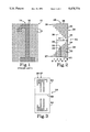
- FIG. 1 illustrates a matrix of dot locations in which a predetermined subset of the dot locations have been marked so that the marked dots together form the alphanumeric character "1".
- FIG. 2 illustrates an adjacent pair of matrices of dot locations for marking a wafer with two copies of an encoded identifying number according to the present invention.
- FIG. 3 illustrates a pair of adjacent dot arrays marked on a wafer surface, each dot array including an encoded representation of a wafer identifying number in accordance with the present invention.
- FIG. 4 illustrates four alternative markings of an identifying number on a wafer, each marking including an alphanumeric representation of the identifying number and a plurality of dot arrays, each dot array containing an encoded representation of the wafer identifying number.
- FIG. 1 shows an alphanumeric character ("1") represented in a matrix 10 of dot locations as is known in the prior art.
- the matrix 10 consists of 16 columns by 23 rows of dot locations, each location being indicated by a small circle, for example dot locations 12.
- a predetermined alphanumeric character 14, here the number one, is formed in the matrix 10 by writing on (or filling in) a predetermined subset of the dot locations, for example, by use of a laser scribe, to form dots, e.g., dots 16, which together form the character.
- dots e.g., dots 16 which together form the character.
- a series of alphanumeric characters can be marked onto a wafer in this fashion, as further discussed below with regard to FIG. 4, to form a complete wafer identifying number.
- FIG. 2 illustrates the general arrangement of a binary dot-array encoding system for marking an identifying number on a semiconductor wafer according to the present invention.
- a first matrix of dot locations 20 is shown below a second matrix 30 of equal size.
- Each matrix 20, 30 includes a matrix of dot locations defining a series of parallel columns.
- a predetermined wafer identifying number is encoded as follows. Each digit of the number is represented by a contiguous series of dots scribed or marked in a corresponding column of dot locations in the matrix. The number of dots marked in each column is equal to the numeric value of the corresponding digit plus one dot, illustrated by the formula:
- N is the numeral value of the digit and n is the same value expressed in scribed dots.
- the marked dots together form a dot array.
- the dot locations are marked by a laser scribe system, for example, the Wafermark 200HS available from Lumonics of Camarillo, Calif.
- FIG. 2 illustrates this encoding scheme.
- the FIG. not all dot locations in the matrix are indicated, to improve clarity. Rather, small circles are shown to indicate the dot locations to be marked to encode each of the numerals zero through ten.
- the alphanumeric equivalent of each column of dots is shown below the corresponding column. For example, a series of six dots (28) are shown in the column labeled "5". The unmarked dot locations are not shown.
- Matrix 20 is circumscribed by a dashed line 24 which includes a horizontal baseline 25.
- a first row of dot locations 27 extends along the baseline 25. These are referred to as origin dot locations.
- a series of dot locations are marked which includes the required number of dots (determined as described above), marked on a contiguous series of dot locations that beings at the origin dot location. This arrangement has several advantages explained below.
- dots are marked on the wafer in the dot locations indicated by the column of circles aligned over the respective digit.
- the numeral 7 there are eight circles in the column above the numeral 7.
- dots would be marked on the wafer in each of the eight dot locations represented by the circles 22.
- the first row 27 of dot locations will always be marked. This feature provides a convenient reference for a vision system to read the coded wafer ID number, discussed further below.
- Each column has a height that corresponds to ten dot locations.
- the width of each field is sized to include a number of columns at least equal to the number of digits in a desired wafer identifying number. According to an operative example of the invention, seven columns are used. Accordingly, the dashed line 24 which circumscribes field 20 includes seven columns. Seven digits of identifying numbers could be allocated, for example, to provide a one-digit fab number, a four-digit lot number and a two-digit wafer number.
- Matrix 30 has the same height (ten dot locations) and the same width (seven dot locations or columns) as matrix 20.
- Matrix 3 is positioned in adjacent registration with matrix 20 such that each column of the second matrix is collinear with the corresponding column of the first matrix, for reasons explained below.
- Matrix 30 is inverted with respect to matrix 20 about dashed line 41. Accordingly, dashed line 35 along the top of the figure defines the baseline of matrix 30.
- dots are marked on the wafer in a number of dot locations in each column that corresponds to the respective digit, as explained above. Here, however, the dots are marked on a contiguous series of dot locations that begins at the baseline 35 and extends downward in the figure. For example, a series of dots 38 consists of six dots, representing the number five, in the column labeled "5".
- a first row 39 of dot locations along baseline 38 of matrix 30 will always be marked, again providing a reference for an automated vision system.
- the dot array coding described dramatically reduces the required field size for a vision system to capture, read and determine the wafer number. For example, eight fields of the type shown in FIG. 1 are required to encode a wafer number, whereas the matrix pair 20, 30 of FIG. 2 encodes the same wafer number twice.
- the baseline row 27 provides a reference line for the vision system.
- the baseline row preferably consists of at least eight dots, though the number may be varied, for example, in accordance with the number of digits to be encoded.
- Each column of dots, representing a digit extends perpendicular to the baseline beginning with the origin dot in the baseline row.
- the baseline rows 27, 39 are parallel to each other and spaced apart by a predetermined distance, for simple and reliable orientation of the vision system. They must be spaced at least 20 dot positions apart so the fields do not overlap.
- a vision system suitable for practicing the present invention is a model 386HR available from Intelledex of Corvallis, Oreg.
- the vision system is arranged to scan the wafer and capture data representing an image of the dot array.
- a vision system can easily recognize each scribed dot and check its location in one or more of a variety of ways. For example, each column of dots must be contiguous from the baseline row. If any dot location is unmarked, but a dot is detected "higher up" in the same column, the marking is defective.
- location of the "highest” dot in each column can be compared to the corresponding dot in the other array of a dot-array pair.
- “highest” means furthest from the applicable baseline row. The distance of the highest dot from the baseline row of dots determines the indicated digit value.
- K is a constant, fixed value +/- a definable error or tolerance.
- X is the column number or position, so generally Xl equals X2.
- Y is the distance from the corresponding baseline or baseline row of dots.
- the likelihood is that, where one field of a pair is defective, the other is not.
- three fields, each containing a redundant representation of the same wafer identifying number, are provided.
- a simple voting algorithm can be applied to determine which array, if any, is defective and ignore it. The identification of the wafer is not lost, however, as the non-defective dot arrays can be used to recover the wafer identifying number.
- FIG. 3 illustrates an example of a wafer surface 50 that has been marked with a predetermined identifying number (3271701) according to the present invention.
- the surface 50 includes a first field, circumscribed by dashed line 52, and a second field of equal size, circumscribed by dashed line 54.
- Each field includes a dot array that represents the wafer identifying number.
- Each dot of the array is inscribed on one of a predetermined matrix of dot locations on the wafer.
- the matrix includes seven columns and ten rows, as explained above with respect to FIG. 2.
- the first column 55 is marked in four successive dot locations, beginning at the base location. These four dots encode the digit "3" as explained above.
- the third column 57 is marked in eight successive dot locations, beginning at the base location, to represent the digit "7.”
- each of the other columns can be decoded into their respective digits.
- the series of decoded digits can be assembled to form the wafer identifying number, here equal to 3271701.
- the second field 54 is identical to the first field 52, albeit inverted about the horizontal axis 59.
- the fields are aligned so that corresponding columns are collinear.
- Field 54 includes a second dot array identical to the array described above in field 52.
- the second array thus provides a duplicate of the complete wafer identifying number.
- the first and second dot arrays together form an array pair, amenable to validity checking as described previously.
- FIG. 4 illustrates a series of alternative methods of marking an identifying number on a wafer surface.
- Each subpart of the FIG. A-D includes an alphanumeric representation 60 of the wafer identifying number "32717-01.”
- the alphanumeric representations may conveniently be formed of dots as illustrated in FIG. 1.
- the wafer is also marked with a pair of dot arrays, indicated by dashed box 50.
- Box 50 represents a dot-array pair such as the array pair of FIG. 3.
- the exact location of the dot array marking is not critical, as long as it does not overlap the alphanumeric marking 60.
- This FIG. illustrates the relative sizes or wafer area required for these two types of markings. While the pair 50 of dot arrays contains two copies of the wafer identifying number, it occupies a total area equal to about 90% of the wafer area occupied by a single digit of the alphanumeric representation 60.
- the alphanumeric version and the dot array version of the wafer identifying number are redundant, as they contain the same information.
- the dot array code version is superior for machine reading, as it is more reliable and subject to error checking as described above.
- the hyphen in the alphanumeric representation may be omitted in the dot array encoding because it is unnecessary for the computer system to distinguish, for example, a lot number from wafer number.
- FIG. 4(B) illustrates an alternative wafer marking which includes two copies of the dot array pair 50, for a total of four dot-array encoded copies of the wafer identifying number.
- Each dot array pair can be checked for validity, as explained. An invalid pair can be detected and ignored for purposes of identifying the wafer.
- the dot arrays are shown adjacent the alphanumeric representation. This has the advantage of minimizing the total wafer area dedicated to identification markings.
- the alphanumeric representation 60 may be omitted, but it is convenient for human determination of the wafer number, under appropriate magnification.
- alphanumeric characters are formed in a 23 by 15 dot array, as illustrated in FIG. 1.
- a nominal center-to-center dot size is on the order of two microns.
- the 23 by 15 dot array thus would occupy a wafer area on the order of 50 by 30 microns. Additional space is provided between alphanumeric characters to make them more readable.
- a 100 x magnification, for example, would produce an apparent character height of about five millimeters or approximately 1/4 inch.
- a pair of dot arrays, such as pair 50 which includes two copies of the wafer identifying number, measures about 7 columns by 20 rows. Again assuming a two-micron nominal dot size, the pair of dot arrays would measure only about 14 by 40 microns.
- FIG. 4(c) illustrates another alternative embodiment which includes a dot array pair 50 and a single dot array 54.
- Array 54 contains another copy of the wafer identifying number, encoded as described above. This embodiment thus provides three encoded copies of the identifying number, a convenient arrangement for employing a two-out-of-three voting mechanism for detecting a defective copy.
- FIG. 4(d) illustrates yet another alternative embodiment which includes the dot array pair 50, a second dot array pair 54 and a third array pair 56.
- Arrays 50 and 54 provide three copies of the identifying number as described above.
- Array 56 provides yet a fourth copy of the identifying number for additional redundancy at minimal additional cost in terms of wafer area.
Abstract
Description
n=N+1dot
Claims (2)
Priority Applications (1)
| Application Number | Priority Date | Filing Date | Title |
|---|---|---|---|
| US07/598,110 US5175774A (en) | 1990-10-16 | 1990-10-16 | Semiconductor wafer marking for identification during processing |
Applications Claiming Priority (1)
| Application Number | Priority Date | Filing Date | Title |
|---|---|---|---|
| US07/598,110 US5175774A (en) | 1990-10-16 | 1990-10-16 | Semiconductor wafer marking for identification during processing |
Publications (1)
| Publication Number | Publication Date |
|---|---|
| US5175774A true US5175774A (en) | 1992-12-29 |
Family
ID=24394278
Family Applications (1)
| Application Number | Title | Priority Date | Filing Date |
|---|---|---|---|
| US07/598,110 Expired - Lifetime US5175774A (en) | 1990-10-16 | 1990-10-16 | Semiconductor wafer marking for identification during processing |
Country Status (1)
| Country | Link |
|---|---|
| US (1) | US5175774A (en) |
Cited By (56)
| Publication number | Priority date | Publication date | Assignee | Title |
|---|---|---|---|---|
| FR2738650A1 (en) * | 1995-09-13 | 1997-03-14 | Moussette Jean Pierre Roger De | METHOD OF RECOGNITION BY OPTOELECTRONIC READING OF ALPHANUMERIC AND SYMBOLIC SIGNS WITH HAND-WRITTEN OR PRINTED FILLING |
| WO1998005427A1 (en) * | 1996-08-01 | 1998-02-12 | Micronic B.V. | Test tube with optically readable coding |
| US5774022A (en) * | 1996-08-29 | 1998-06-30 | Micron Communications, Inc. | Digital clock recovery loop |
| US5890807A (en) * | 1995-10-28 | 1999-04-06 | Deutsche Itt Industries Gmbh | Method for identifying an apparatus or device utilizing a randomly produced characteristic thereof |
| US5894172A (en) * | 1996-05-27 | 1999-04-13 | Mitsubishi Denki Kabushiki Kaisha | Semiconductor device with identification function |
| EP0927947A2 (en) * | 1997-12-03 | 1999-07-07 | Miyachi Technos Corporation | Two-dimensional bar code laser marking method |
| US5970398A (en) * | 1996-07-30 | 1999-10-19 | Micron Communications, Inc. | Radio frequency antenna with current controlled sensitivity |
| US6049624A (en) * | 1998-02-20 | 2000-04-11 | Micron Technology, Inc. | Non-lot based method for assembling integrated circuit devices |
| US6100765A (en) * | 1998-01-09 | 2000-08-08 | Micron Technology, Inc. | Digital clock recovery loop |
| US6130602A (en) * | 1996-05-13 | 2000-10-10 | Micron Technology, Inc. | Radio frequency data communications device |
| US6147321A (en) * | 1997-08-01 | 2000-11-14 | Infineon Technologies Ag | Configuration for the automatic inscription or reinscription of wafers |
| US6248973B1 (en) * | 1998-03-11 | 2001-06-19 | Komatsu Limited | Laser marking method for semiconductor wafer |
| US6265684B1 (en) * | 1999-10-28 | 2001-07-24 | Promos Technologies Inc. | Wafer ID optical sorting system |
| US6268641B1 (en) | 1998-03-30 | 2001-07-31 | Kabushiki Kaisha Toshiba | Semiconductor wafer having identification indication and method of manufacturing the same |
| US6303899B1 (en) * | 1998-12-11 | 2001-10-16 | Lsi Logic Corporation | Method and apparatus for scribing a code in an inactive outer clear out area of a semiconductor wafer |
| US6315202B2 (en) * | 1997-08-11 | 2001-11-13 | Technolines, Llc. | Material coding using lasers |
| US20020031732A1 (en) * | 2000-08-24 | 2002-03-14 | Tdk Corporation | Method for imprinting a wafer with identifying information, and exposing method and apparatus for imprinting a wafer with identifying information |
| US20020088743A1 (en) * | 1997-01-17 | 2002-07-11 | Beffa Raymond J. | Method for sorting integrated circuit devices |
| US6466131B1 (en) | 1996-07-30 | 2002-10-15 | Micron Technology, Inc. | Radio frequency data communications device with adjustable receiver sensitivity and method |
| US20030036025A1 (en) * | 2001-08-09 | 2003-02-20 | Taisuke Hirooka | Method of recording identifier and set of photomasks |
| US20030059726A1 (en) * | 2001-09-05 | 2003-03-27 | Sumitomo Special Metals Co., Ltd. | Method of recording identifier and set of photomasks |
| US6696879B1 (en) | 1996-05-13 | 2004-02-24 | Micron Technology, Inc. | Radio frequency data communications device |
| US6774340B1 (en) * | 1998-11-25 | 2004-08-10 | Komatsu Limited | Shape of microdot mark formed by laser beam and microdot marking method |
| US6774685B2 (en) | 1996-05-13 | 2004-08-10 | Micron Technology, Inc. | Radio frequency data communications device |
| US20040156529A1 (en) * | 1994-03-17 | 2004-08-12 | Davis Bruce L. | Methods and tangible objects employing textured machine readable data |
| US6792365B2 (en) | 2001-08-10 | 2004-09-14 | Micron Technology, Inc. | Sequential unique marking |
| US6836468B1 (en) | 1996-05-13 | 2004-12-28 | Micron Technology, Inc. | Radio frequency data communications device |
| US6941124B1 (en) | 1996-05-13 | 2005-09-06 | Micron Technology, Inc. | Method of speeding power-up of an amplifier, and amplifier |
| US7007855B1 (en) | 2000-03-17 | 2006-03-07 | International Business Machines Corporation | Wafer identification mark |
| US7107117B2 (en) | 1997-02-17 | 2006-09-12 | Micron Technology, Inc. | Sorting a group of integrated circuit devices for those devices requiring special testing |
| US7124050B2 (en) | 1997-02-26 | 2006-10-17 | Micron Technology, Inc. | Method in an integrated circuit (IC) manufacturing process for identifying and redirecting IC's mis-processed during their manufacture |
| US7155300B2 (en) | 1997-06-06 | 2006-12-26 | Micron Technology, Inc. | Method for using data regarding manufacturing procedures integrated circuits (IC's) have undergone, such as repairs, to select procedures the IC's will undergo, such as additional repairs |
| US20070170381A1 (en) * | 2000-04-04 | 2007-07-26 | Little Joseph R | Semiconductor device structure that includes markings covered by visibly opaque materials |
| US20070209447A1 (en) * | 2006-03-10 | 2007-09-13 | Northrop Grumman Corporation | In-situ large area optical strain measurement using an encoded dot pattern |
| US20070222611A1 (en) * | 2000-04-26 | 2007-09-27 | Micron Technology, Inc. | Automated antenna trim for transmitting and receiving semiconductor devices |
| US7276672B2 (en) | 1997-01-17 | 2007-10-02 | Micron Technology, Inc. | Method for sorting integrated circuit devices |
| US20070239307A1 (en) * | 1997-03-24 | 2007-10-11 | Jones Mark L | Process and method for continuous, non lot-based integrated circuit manufacturing |
| CN100346394C (en) * | 2004-04-20 | 2007-10-31 | 阿尔卑斯电气株式会社 | Film magnetic head and its individual identification method |
| US20080048018A1 (en) * | 1998-09-11 | 2008-02-28 | Davis Bruce L | Methods, Objects and Apparatus Employing Machine Readable Data |
| US20080266192A1 (en) * | 2007-04-26 | 2008-10-30 | Micron Technology, Inc. | Methods and systems of changing antenna polarization |
| US20090058649A1 (en) * | 2007-08-31 | 2009-03-05 | Micron Technology, Inc. | Selectively coupling to feed points of an antenna system |
| US7561938B2 (en) | 1997-06-06 | 2009-07-14 | Micron Technology, Inc. | Method for using data regarding manufacturing procedures integrated circuits (ICS) have undergone, such as repairs, to select procedures the ICs will undergo, such as additional repairs |
| US20100046838A1 (en) * | 2008-07-24 | 2010-02-25 | Uri Vekstein | System and method for obtaining text |
| US7727785B2 (en) | 2002-02-25 | 2010-06-01 | Micron Technology, Inc. | Wafer back side coating to balance stress from passivation layer on front of wafer and be used as die attach adhesive |
| US20120025344A1 (en) * | 2010-07-29 | 2012-02-02 | Stmicroelectronics S.R.L. | Traceable integrated circuits and production method thereof |
| US8115637B2 (en) | 2008-06-03 | 2012-02-14 | Micron Technology, Inc. | Systems and methods to selectively connect antennas to receive and backscatter radio frequency signals |
| US20130037526A1 (en) * | 2005-10-21 | 2013-02-14 | Orbotech Ltd. | Automatic repair of electric circuits |
| US8505108B2 (en) | 1993-11-18 | 2013-08-06 | Digimarc Corporation | Authentication using a digital watermark |
| US9099481B2 (en) | 2013-03-15 | 2015-08-04 | Semiconductor Components Industries, Llc | Methods of laser marking semiconductor substrates |
| US9136222B2 (en) | 2012-05-11 | 2015-09-15 | GlobalFoundries, Inc. | Chip identification pattern and method of forming |
| US20160069757A1 (en) * | 2013-05-03 | 2016-03-10 | Indian Council Of Medicalresearch | Non-Contact Method for Measurement of Strain Profile at a Location Interposed within a Soft Deformable Object with Dynamic Evolution of the Strain Under Dynamic Loading or Fracture of the Object |
| US20200262229A1 (en) * | 2017-11-07 | 2020-08-20 | Sumitomo Electric Sintered Alloy, Ltd. | Iron-based sintered body, method for laser-marking the same, and method for manufacturing the same |
| US10998285B2 (en) | 2019-01-25 | 2021-05-04 | Omnivision Technologies, Inc. | Code pattern for representing tracing number of chip |
| US20220107967A1 (en) * | 2020-10-06 | 2022-04-07 | SafeGraph, Inc. | Systems and Methods for Generating Multi-Part Place Identifiers |
| US20220301907A1 (en) * | 2019-08-23 | 2022-09-22 | Ev Group E. Thallner Gmbh | Method and device for the alignment of substrates |
| US11562928B2 (en) | 2019-01-25 | 2023-01-24 | Omnivision Technologies, Inc. | Laser marked code pattern for representing tracing number of chip |
Citations (6)
| Publication number | Priority date | Publication date | Assignee | Title |
|---|---|---|---|---|
| US3470357A (en) * | 1963-06-07 | 1969-09-30 | Wilhelm Ritzerfeld | Method of producing a printing form and of evaluating data contained therein |
| US3544771A (en) * | 1967-01-03 | 1970-12-01 | Hughes Aircraft Co | Record medium having character representations thereon |
| US3776454A (en) * | 1969-09-12 | 1973-12-04 | L Jones | Data supports for numerical data |
| US4162035A (en) * | 1977-09-23 | 1979-07-24 | General Signal Corporation | High resolution optical position code detector for information recorded on record carrier partially in humanly intelligible form |
| US4275380A (en) * | 1979-05-30 | 1981-06-23 | Ncr Corporation | Topography for integrated circuits pattern recognition array |
| US4409686A (en) * | 1980-06-16 | 1983-10-11 | Harris Corporation | Method of serialization of dice |
-
1990
- 1990-10-16 US US07/598,110 patent/US5175774A/en not_active Expired - Lifetime
Patent Citations (6)
| Publication number | Priority date | Publication date | Assignee | Title |
|---|---|---|---|---|
| US3470357A (en) * | 1963-06-07 | 1969-09-30 | Wilhelm Ritzerfeld | Method of producing a printing form and of evaluating data contained therein |
| US3544771A (en) * | 1967-01-03 | 1970-12-01 | Hughes Aircraft Co | Record medium having character representations thereon |
| US3776454A (en) * | 1969-09-12 | 1973-12-04 | L Jones | Data supports for numerical data |
| US4162035A (en) * | 1977-09-23 | 1979-07-24 | General Signal Corporation | High resolution optical position code detector for information recorded on record carrier partially in humanly intelligible form |
| US4275380A (en) * | 1979-05-30 | 1981-06-23 | Ncr Corporation | Topography for integrated circuits pattern recognition array |
| US4409686A (en) * | 1980-06-16 | 1983-10-11 | Harris Corporation | Method of serialization of dice |
Cited By (158)
| Publication number | Priority date | Publication date | Assignee | Title |
|---|---|---|---|---|
| US8505108B2 (en) | 1993-11-18 | 2013-08-06 | Digimarc Corporation | Authentication using a digital watermark |
| US20050180599A1 (en) * | 1994-03-17 | 2005-08-18 | Davis Bruce L. | Methods and tangible objects employing textured machine readable data |
| US7076084B2 (en) | 1994-03-17 | 2006-07-11 | Digimarc Corporation | Methods and objects employing machine readable data |
| US6882738B2 (en) | 1994-03-17 | 2005-04-19 | Digimarc Corporation | Methods and tangible objects employing textured machine readable data |
| US20040156529A1 (en) * | 1994-03-17 | 2004-08-12 | Davis Bruce L. | Methods and tangible objects employing textured machine readable data |
| US7305117B2 (en) * | 1994-03-17 | 2007-12-04 | Digimarc Corporation | Methods and tangible objects employing machine readable data |
| WO1997010565A1 (en) * | 1995-09-13 | 1997-03-20 | Moussette Jean Pierre | Indicia device and optical scanning method |
| FR2738650A1 (en) * | 1995-09-13 | 1997-03-14 | Moussette Jean Pierre Roger De | METHOD OF RECOGNITION BY OPTOELECTRONIC READING OF ALPHANUMERIC AND SYMBOLIC SIGNS WITH HAND-WRITTEN OR PRINTED FILLING |
| US5890807A (en) * | 1995-10-28 | 1999-04-06 | Deutsche Itt Industries Gmbh | Method for identifying an apparatus or device utilizing a randomly produced characteristic thereof |
| US6721289B1 (en) | 1996-05-13 | 2004-04-13 | Micron Technology, Inc. | Radio frequency data communications device |
| US6771613B1 (en) | 1996-05-13 | 2004-08-03 | Micron Technology, Inc. | Radio frequency data communications device |
| US6941124B1 (en) | 1996-05-13 | 2005-09-06 | Micron Technology, Inc. | Method of speeding power-up of an amplifier, and amplifier |
| US6492192B1 (en) | 1996-05-13 | 2002-12-10 | Micron Technology, Inc. | Method of making a Schottky diode in an integrated circuit |
| US6130602A (en) * | 1996-05-13 | 2000-10-10 | Micron Technology, Inc. | Radio frequency data communications device |
| US7079043B2 (en) | 1996-05-13 | 2006-07-18 | Micron Technology, Inc. | Radio frequency data communications device |
| US6157230A (en) * | 1996-05-13 | 2000-12-05 | Micron Technology, Inc. | Method for realizing an improved radio frequency detector for use in a radio frequency identification device, frequency lock loop, timing oscillator, method of constructing a frequency lock loop and method of operating an integrated circuit |
| US6198357B1 (en) | 1996-05-13 | 2001-03-06 | Micron Technology, Inc. | Stage having controlled variable resistance load circuit for use in voltage controlled ring oscillator |
| US6198332B1 (en) | 1996-05-13 | 2001-03-06 | Micron Technology, Inc. | Frequency doubler and method of doubling frequency |
| US6836472B2 (en) | 1996-05-13 | 2004-12-28 | Micron Technology, Inc. | Radio frequency data communications device |
| US7545256B2 (en) | 1996-05-13 | 2009-06-09 | Keystone Technology Solutions, Llc | System and method for identifying a radio frequency identification (RFID) device |
| US6249185B1 (en) | 1996-05-13 | 2001-06-19 | Micron Technology, Inc. | Method of speeding power-up of an amplifier, and amplifier |
| US6836468B1 (en) | 1996-05-13 | 2004-12-28 | Micron Technology, Inc. | Radio frequency data communications device |
| US6825773B1 (en) | 1996-05-13 | 2004-11-30 | Micron Technology, Inc. | Radio frequency data communications device |
| US6774685B2 (en) | 1996-05-13 | 2004-08-10 | Micron Technology, Inc. | Radio frequency data communications device |
| US6466634B1 (en) | 1996-05-13 | 2002-10-15 | Micron Technology, Inc. | Radio frequency data communications device |
| US6278698B1 (en) | 1996-05-13 | 2001-08-21 | Micron Technology, Inc. | Radio frequency data communications device |
| US6735183B2 (en) | 1996-05-13 | 2004-05-11 | Micron Technology, Inc. | Radio frequency data communications device |
| US6947513B2 (en) | 1996-05-13 | 2005-09-20 | Micron Technology, Inc. | Radio frequency data communications device |
| US6314440B1 (en) | 1996-05-13 | 2001-11-06 | Micron Technology, Inc. | Pseudo random number generator |
| US7385477B2 (en) | 1996-05-13 | 2008-06-10 | Keystone Technology Solutions, Llc | Radio frequency data communications device |
| US6316975B1 (en) | 1996-05-13 | 2001-11-13 | Micron Technology, Inc. | Radio frequency data communications device |
| US6337634B1 (en) | 1996-05-13 | 2002-01-08 | Micron Technology, Inc. | Radio frequency data communications device |
| US6351190B1 (en) | 1996-05-13 | 2002-02-26 | Micron Technology, Inc. | Stage having controlled variable resistance load circuit for use in voltage controlled ring oscillator |
| US6696879B1 (en) | 1996-05-13 | 2004-02-24 | Micron Technology, Inc. | Radio frequency data communications device |
| US6384648B1 (en) | 1996-05-13 | 2002-05-07 | Micron Technology, Inc. | Radio frequency data communications device |
| US7170867B2 (en) | 1996-05-13 | 2007-01-30 | Micron Technology, Inc. | Radio frequency data communications device |
| US6600428B1 (en) | 1996-05-13 | 2003-07-29 | Micron Technology, Inc. | Radio frequency data communications device |
| US5894172A (en) * | 1996-05-27 | 1999-04-13 | Mitsubishi Denki Kabushiki Kaisha | Semiconductor device with identification function |
| US5970398A (en) * | 1996-07-30 | 1999-10-19 | Micron Communications, Inc. | Radio frequency antenna with current controlled sensitivity |
| US20070075837A1 (en) * | 1996-07-30 | 2007-04-05 | Tuttle Mark E | Radio frequency data communications device with selectively removable antenna portion and method |
| US6509837B1 (en) | 1996-07-30 | 2003-01-21 | Micron Technology, Inc. | Radio frequency data communications device with adjustable receiver sensitivity and method |
| US7345575B2 (en) | 1996-07-30 | 2008-03-18 | Micron Technology, Inc. | Radio frequency data communications device with adjustable receiver sensitivity and method |
| US6781508B2 (en) | 1996-07-30 | 2004-08-24 | Micron Technology Inc | Radio frequency data communications device with adjustable receiver sensitivity and method |
| US7283035B2 (en) | 1996-07-30 | 2007-10-16 | Micron Technology, Inc. | Radio frequency data communications device with selectively removable antenna portion and method |
| US6574454B1 (en) | 1996-07-30 | 2003-06-03 | Micron Technology, Inc. | Radio frequency antenna with current controlled sensitivity |
| US6122494A (en) * | 1996-07-30 | 2000-09-19 | Micron Technology, Inc. | Radio frequency antenna with current controlled sensitivity |
| US6466131B1 (en) | 1996-07-30 | 2002-10-15 | Micron Technology, Inc. | Radio frequency data communications device with adjustable receiver sensitivity and method |
| US8624711B2 (en) | 1996-07-30 | 2014-01-07 | Round Rock Research, Llc | Radio frequency identification device operating methods, radio frequency identification device configuration methods, and radio frequency identification devices |
| US20080100422A1 (en) * | 1996-07-30 | 2008-05-01 | Tuttle Mark E | Radio Frequency Identification Device Operating Methods, Radio Frequency Identification Device Configuration Methods, and Radio Frequency Identification Devices |
| US7884724B2 (en) | 1996-07-30 | 2011-02-08 | Round Rock Research, Llc | Radio frequency data communications device with selectively removable antenna portion and method |
| US20060143899A1 (en) * | 1996-07-30 | 2006-07-06 | Tuttle Mark E | Radio frequency data communications device with selectively removable antenna portion and method |
| US20040085190A1 (en) * | 1996-07-30 | 2004-05-06 | Tuttle Mark E. | Radio frequency data communications device with adjustable receiver sensitivity and method |
| US6270728B1 (en) | 1996-08-01 | 2001-08-07 | Micronic B.V. | Test tube with optically readable coding |
| WO1998005427A1 (en) * | 1996-08-01 | 1998-02-12 | Micronic B.V. | Test tube with optically readable coding |
| US5774022A (en) * | 1996-08-29 | 1998-06-30 | Micron Communications, Inc. | Digital clock recovery loop |
| US6285261B1 (en) | 1996-08-29 | 2001-09-04 | Micron Technology, Inc. | Digital clock recovery loop |
| US5982237A (en) * | 1996-08-29 | 1999-11-09 | Micron Communications, Inc. | Digital clock recovery loop |
| US20020088743A1 (en) * | 1997-01-17 | 2002-07-11 | Beffa Raymond J. | Method for sorting integrated circuit devices |
| US20090038997A1 (en) * | 1997-01-17 | 2009-02-12 | Micron Technology, Inc. | Method for sorting integrated circuit devices |
| US20090060703A1 (en) * | 1997-01-17 | 2009-03-05 | Micron Technology, Inc. | Method for sorting integrated circuit devices |
| US7682847B2 (en) | 1997-01-17 | 2010-03-23 | Micron Technology, Inc. | Method for sorting integrated circuit devices |
| US7875821B2 (en) | 1997-01-17 | 2011-01-25 | Micron Technology, Inc. | Method for sorting integrated circuit devices |
| US20110089088A1 (en) * | 1997-01-17 | 2011-04-21 | Micron Technology, Inc. | Method for sorting integrated circuit devices |
| US7446277B2 (en) | 1997-01-17 | 2008-11-04 | Micron Technology, Inc. | Method for sorting integrated circuit devices |
| US7368678B2 (en) | 1997-01-17 | 2008-05-06 | Micron Technology, Inc. | Method for sorting integrated circuit devices |
| US7276672B2 (en) | 1997-01-17 | 2007-10-02 | Micron Technology, Inc. | Method for sorting integrated circuit devices |
| US7107117B2 (en) | 1997-02-17 | 2006-09-12 | Micron Technology, Inc. | Sorting a group of integrated circuit devices for those devices requiring special testing |
| US7502659B2 (en) | 1997-02-17 | 2009-03-10 | Micron Technology, Inc. | Sorting a group of integrated circuit devices for those devices requiring special testing |
| US7117063B2 (en) | 1997-02-17 | 2006-10-03 | Micro Technology, Inc. | Sorting a group of integrated circuit devices for those devices requiring special testing |
| US7124050B2 (en) | 1997-02-26 | 2006-10-17 | Micron Technology, Inc. | Method in an integrated circuit (IC) manufacturing process for identifying and redirecting IC's mis-processed during their manufacture |
| US7885782B2 (en) | 1997-02-26 | 2011-02-08 | Micron Technology, Inc. | Method in an integrated circuit (IC) manufacturing process for identifying and redirecting ICs mis-processed during their manufacture |
| US20100222913A1 (en) * | 1997-03-24 | 2010-09-02 | Micron Technology, Inc. | Methods for non lot-based integrated circuit manufacturing |
| US7738988B2 (en) | 1997-03-24 | 2010-06-15 | Micron Technology, Inc. | Process and method for continuous, non lot-based integrated circuit manufacturing |
| US7555358B2 (en) | 1997-03-24 | 2009-06-30 | Micron Technology, Inc. | Process and method for continuous, non lot-based integrated circuit manufacturing |
| US8600540B2 (en) | 1997-03-24 | 2013-12-03 | Micron Technology, Inc. | Methods for non-lot-based manufacturing of articles |
| US8315730B2 (en) | 1997-03-24 | 2012-11-20 | Micron Technology, Inc. | Methods for non lot-based integrated circuit manufacturing |
| US20070239307A1 (en) * | 1997-03-24 | 2007-10-11 | Jones Mark L | Process and method for continuous, non lot-based integrated circuit manufacturing |
| US7561938B2 (en) | 1997-06-06 | 2009-07-14 | Micron Technology, Inc. | Method for using data regarding manufacturing procedures integrated circuits (ICS) have undergone, such as repairs, to select procedures the ICs will undergo, such as additional repairs |
| US7155300B2 (en) | 1997-06-06 | 2006-12-26 | Micron Technology, Inc. | Method for using data regarding manufacturing procedures integrated circuits (IC's) have undergone, such as repairs, to select procedures the IC's will undergo, such as additional repairs |
| US6147321A (en) * | 1997-08-01 | 2000-11-14 | Infineon Technologies Ag | Configuration for the automatic inscription or reinscription of wafers |
| US6315202B2 (en) * | 1997-08-11 | 2001-11-13 | Technolines, Llc. | Material coding using lasers |
| EP0927947A2 (en) * | 1997-12-03 | 1999-07-07 | Miyachi Technos Corporation | Two-dimensional bar code laser marking method |
| CN1116653C (en) * | 1997-12-03 | 2003-07-30 | 宫地技术株式会社 | Two-dimensional bar code laser marking method |
| EP0927947A3 (en) * | 1997-12-03 | 2001-04-25 | Miyachi Technos Corporation | Two-dimensional bar code laser marking method |
| US6121574A (en) * | 1997-12-03 | 2000-09-19 | Miyachi Technos Corporation | Two-dimensional bar code laser marking method |
| US6100765A (en) * | 1998-01-09 | 2000-08-08 | Micron Technology, Inc. | Digital clock recovery loop |
| US6049624A (en) * | 1998-02-20 | 2000-04-11 | Micron Technology, Inc. | Non-lot based method for assembling integrated circuit devices |
| US6226394B1 (en) | 1998-02-20 | 2001-05-01 | Micron Tecnology, Inc. | Non-lot based method for assembling integrated circuit devices |
| US7120287B2 (en) | 1998-02-20 | 2006-10-10 | Micron Technology, Inc. | Non-lot based method for assembling integrated circuit devices |
| US6400840B2 (en) | 1998-02-20 | 2002-06-04 | Micron Technology, Inc. | Non-lot based method for assembling integrated circuit devices |
| US20040005090A1 (en) * | 1998-02-20 | 2004-01-08 | Kevin Wilson | Non-lot based method for assembling integrated circuit devices |
| US6588854B2 (en) | 1998-02-20 | 2003-07-08 | Micron Technology, Inc. | Nonlot based method for assembling integrated circuit devices |
| US6248973B1 (en) * | 1998-03-11 | 2001-06-19 | Komatsu Limited | Laser marking method for semiconductor wafer |
| US6544804B2 (en) | 1998-03-30 | 2003-04-08 | Kabushiki Kaisha Toshiba | Semiconductor wafer having identification indication and method of manufacturing the same |
| US6268641B1 (en) | 1998-03-30 | 2001-07-31 | Kabushiki Kaisha Toshiba | Semiconductor wafer having identification indication and method of manufacturing the same |
| US20080048018A1 (en) * | 1998-09-11 | 2008-02-28 | Davis Bruce L | Methods, Objects and Apparatus Employing Machine Readable Data |
| US7548643B2 (en) * | 1998-09-11 | 2009-06-16 | Digimarc Corporation | Methods, objects and apparatus employing machine readable data |
| US8000518B2 (en) * | 1998-09-11 | 2011-08-16 | Digimarc Corporation | Methods, objects and apparatus employing machine readable data |
| US20090252401A1 (en) * | 1998-09-11 | 2009-10-08 | Davis Bruce L | Methods, Objects and Apparatus Employing Machine Readable Data |
| US6774340B1 (en) * | 1998-11-25 | 2004-08-10 | Komatsu Limited | Shape of microdot mark formed by laser beam and microdot marking method |
| US6303899B1 (en) * | 1998-12-11 | 2001-10-16 | Lsi Logic Corporation | Method and apparatus for scribing a code in an inactive outer clear out area of a semiconductor wafer |
| US6265684B1 (en) * | 1999-10-28 | 2001-07-24 | Promos Technologies Inc. | Wafer ID optical sorting system |
| US7510124B2 (en) | 2000-03-17 | 2009-03-31 | International Business Machines Corporation | Wafer identification mark |
| US7007855B1 (en) | 2000-03-17 | 2006-03-07 | International Business Machines Corporation | Wafer identification mark |
| US20070241202A1 (en) * | 2000-03-17 | 2007-10-18 | International Business Machines Corporation | Wafer identification mark |
| US20070170381A1 (en) * | 2000-04-04 | 2007-07-26 | Little Joseph R | Semiconductor device structure that includes markings covered by visibly opaque materials |
| US7253428B1 (en) | 2000-04-04 | 2007-08-07 | Micron Technology, Inc. | Apparatus and method for feature edge detection in semiconductor processing |
| US20070222611A1 (en) * | 2000-04-26 | 2007-09-27 | Micron Technology, Inc. | Automated antenna trim for transmitting and receiving semiconductor devices |
| US20070290861A1 (en) * | 2000-04-26 | 2007-12-20 | Micron Technology, Inc. | Automated antenna trim for transmitting and receiving semiconductor devices |
| US8134467B2 (en) | 2000-04-26 | 2012-03-13 | Round Rock Research, Llc | Automated antenna trim for transmitting and receiving semiconductor devices |
| US7812728B2 (en) | 2000-04-26 | 2010-10-12 | Round Rock Research, Llc | Methods and apparatuses for radio frequency identification (RFID) tags configured to allow antenna trim |
| US20020031732A1 (en) * | 2000-08-24 | 2002-03-14 | Tdk Corporation | Method for imprinting a wafer with identifying information, and exposing method and apparatus for imprinting a wafer with identifying information |
| US6731373B2 (en) * | 2000-08-24 | 2004-05-04 | Tdk Corporation | Method for imprinting a wafer with identifying information, and exposing method and apparatus for imprinting a wafer with identifying information |
| US20030036025A1 (en) * | 2001-08-09 | 2003-02-20 | Taisuke Hirooka | Method of recording identifier and set of photomasks |
| US6924090B2 (en) | 2001-08-09 | 2005-08-02 | Neomax Co., Ltd. | Method of recording identifier and set of photomasks |
| US20050277210A1 (en) * | 2001-08-10 | 2005-12-15 | Raitter James S | Sequential unique marking |
| US6792365B2 (en) | 2001-08-10 | 2004-09-14 | Micron Technology, Inc. | Sequential unique marking |
| US20050014327A1 (en) * | 2001-08-10 | 2005-01-20 | Raitter James S. | Sequential unique marking |
| US7440860B2 (en) | 2001-08-10 | 2008-10-21 | Micron Technology, Inc. | Sequential unique marking |
| US6996484B2 (en) * | 2001-08-10 | 2006-02-07 | Micron Technology, Inc. | Sequential unique marking |
| US20030059726A1 (en) * | 2001-09-05 | 2003-03-27 | Sumitomo Special Metals Co., Ltd. | Method of recording identifier and set of photomasks |
| US6897010B2 (en) * | 2001-09-05 | 2005-05-24 | Neomax Co., Ltd. | Method of recording identifier and set of photomasks |
| US7727785B2 (en) | 2002-02-25 | 2010-06-01 | Micron Technology, Inc. | Wafer back side coating to balance stress from passivation layer on front of wafer and be used as die attach adhesive |
| CN100346394C (en) * | 2004-04-20 | 2007-10-31 | 阿尔卑斯电气株式会社 | Film magnetic head and its individual identification method |
| US20130037526A1 (en) * | 2005-10-21 | 2013-02-14 | Orbotech Ltd. | Automatic repair of electric circuits |
| US20070209447A1 (en) * | 2006-03-10 | 2007-09-13 | Northrop Grumman Corporation | In-situ large area optical strain measurement using an encoded dot pattern |
| US7377181B2 (en) | 2006-03-10 | 2008-05-27 | Northrop Grumman Corporation | In-situ large area optical strain measurement using an encoded dot pattern |
| US20110032171A1 (en) * | 2007-04-26 | 2011-02-10 | Round Rock Research, Llc | Methods and systems of changing antenna polarization |
| US7825867B2 (en) | 2007-04-26 | 2010-11-02 | Round Rock Research, Llc | Methods and systems of changing antenna polarization |
| US7932867B2 (en) | 2007-04-26 | 2011-04-26 | Round Rock Research, Llc | Methods and systems of changing antenna polarization |
| US20080266192A1 (en) * | 2007-04-26 | 2008-10-30 | Micron Technology, Inc. | Methods and systems of changing antenna polarization |
| US7936268B2 (en) | 2007-08-31 | 2011-05-03 | Round Rock Research, Llc | Selectively coupling to feed points of an antenna system |
| US20090058649A1 (en) * | 2007-08-31 | 2009-03-05 | Micron Technology, Inc. | Selectively coupling to feed points of an antenna system |
| US10685195B2 (en) | 2008-06-03 | 2020-06-16 | Micron Technology, Inc. | Systems and methods to selectively connect antennas to receive and backscatter radio frequency signals |
| US11120234B2 (en) | 2008-06-03 | 2021-09-14 | Micron Technology, Inc. | Systems and methods to selectively connect antennas to receive and backscatter radio frequency signals |
| US8115637B2 (en) | 2008-06-03 | 2012-02-14 | Micron Technology, Inc. | Systems and methods to selectively connect antennas to receive and backscatter radio frequency signals |
| US8963719B2 (en) | 2008-06-03 | 2015-02-24 | Micron Technology, Inc. | Systems and methods to selectively connect antennas to receive and backscatter radio frequency signals |
| US10311261B2 (en) | 2008-06-03 | 2019-06-04 | Micron Technology, Inc. | Systems and methods to selectively connect antennas to receive and backscatter radio frequency signals |
| US8405509B2 (en) | 2008-06-03 | 2013-03-26 | Micron Technology, Inc. | Systems and methods to selectively connect antennas to receive and backscatter radio frequency signals |
| US9652645B2 (en) | 2008-06-03 | 2017-05-16 | Micron Technology, Inc. | Systems and methods to selectively connect antennas to receive and backscatter radio frequency signals |
| US11663424B2 (en) | 2008-06-03 | 2023-05-30 | Micron Technology, Inc. | Systems and methods to selectively connect antennas to communicate via radio frequency signals |
| US8315485B2 (en) * | 2008-07-24 | 2012-11-20 | Camtek Ltd. | System and method for obtaining text |
| US20100046838A1 (en) * | 2008-07-24 | 2010-02-25 | Uri Vekstein | System and method for obtaining text |
| US20160079181A1 (en) * | 2010-07-29 | 2016-03-17 | Stmicroelectronics S.R.L. | Traceable integrated circuits and production method thereof |
| US9224694B2 (en) * | 2010-07-29 | 2015-12-29 | Stmicroelectronics S.R.L. | Traceable integrated circuits and production method thereof |
| US20120025344A1 (en) * | 2010-07-29 | 2012-02-02 | Stmicroelectronics S.R.L. | Traceable integrated circuits and production method thereof |
| US9136222B2 (en) | 2012-05-11 | 2015-09-15 | GlobalFoundries, Inc. | Chip identification pattern and method of forming |
| US9355965B2 (en) | 2013-03-15 | 2016-05-31 | Semiconductor Components Industries, Llc | Semiconductor devices and methods of making the same |
| US9099481B2 (en) | 2013-03-15 | 2015-08-04 | Semiconductor Components Industries, Llc | Methods of laser marking semiconductor substrates |
| US9869596B2 (en) * | 2013-05-03 | 2018-01-16 | Indian Council Of Medical Research | Non-contact method for measurement of strain profile at a location interposed within a soft deformable object with dynamic evolution of the strain under dynamic loading or fracture of the object |
| US20160069757A1 (en) * | 2013-05-03 | 2016-03-10 | Indian Council Of Medicalresearch | Non-Contact Method for Measurement of Strain Profile at a Location Interposed within a Soft Deformable Object with Dynamic Evolution of the Strain Under Dynamic Loading or Fracture of the Object |
| US20200262229A1 (en) * | 2017-11-07 | 2020-08-20 | Sumitomo Electric Sintered Alloy, Ltd. | Iron-based sintered body, method for laser-marking the same, and method for manufacturing the same |
| US11660899B2 (en) * | 2017-11-07 | 2023-05-30 | Sumitomo Electric Sintered Alloy. Ltd. | Iron-based sintered body, method for laser-marking the same, and method for manufacturing the same |
| US10998285B2 (en) | 2019-01-25 | 2021-05-04 | Omnivision Technologies, Inc. | Code pattern for representing tracing number of chip |
| US11562928B2 (en) | 2019-01-25 | 2023-01-24 | Omnivision Technologies, Inc. | Laser marked code pattern for representing tracing number of chip |
| US20220301907A1 (en) * | 2019-08-23 | 2022-09-22 | Ev Group E. Thallner Gmbh | Method and device for the alignment of substrates |
| US20220107967A1 (en) * | 2020-10-06 | 2022-04-07 | SafeGraph, Inc. | Systems and Methods for Generating Multi-Part Place Identifiers |
| US11899696B2 (en) * | 2020-10-06 | 2024-02-13 | SafeGraph, Inc. | Systems and methods for generating multi-part place identifiers |
Similar Documents
| Publication | Publication Date | Title |
|---|---|---|
| US5175774A (en) | Semiconductor wafer marking for identification during processing | |
| US5350715A (en) | Chip identification scheme | |
| US4263504A (en) | High density matrix code | |
| US5479004A (en) | Dynamically variable machine readable binary code and method for reading and producing thereof | |
| US6685095B2 (en) | Apparatus and method for decoding damaged optical codes | |
| CN100433038C (en) | Method for reading a symbol having encoded information | |
| EP0484132B1 (en) | Multiple resolution machine readable symbols | |
| US4510673A (en) | Laser written chip identification method | |
| US20120145779A1 (en) | Two-dimensional symbol code and method for reading the symbol code | |
| EP0721630B1 (en) | Packet bar code encoding and decoding | |
| EP0256807B1 (en) | Optical recording card and method of reading the same | |
| GB2255848A (en) | Label carrying encoded data | |
| KR101601367B1 (en) | Method and light pattern for measuring the height or the height profile of an object | |
| US5920062A (en) | Combined linear and two-dimensional bar code structure | |
| GB2252653A (en) | Decoding encoded information | |
| EP0585244A1 (en) | Data tag and detecting method | |
| US8881985B2 (en) | Method for the concretizing of a substrate | |
| US20180342411A1 (en) | Chip identification system | |
| JPS62237585A (en) | Optical type object identifier | |
| US7188778B2 (en) | Machine-readable symbol and related method | |
| EP0699324B1 (en) | A method and apparatus for identifying the orientation of a dot matrix code marking of an article | |
| US6687403B1 (en) | Process and device for detection of straight-line segments in a stream of digital data that are representative of an image in which the contour points of said image are identified | |
| US20060289661A1 (en) | Bi-directional readable two-dimensional bar code system and its reading method | |
| US20030001019A1 (en) | Computer-and human-readable part markings and system and method using same | |
| EP0736835B1 (en) | Process for reading a dot matrix code marking on an article |
Legal Events
| Date | Code | Title | Description |
|---|---|---|---|
| AS | Assignment |
Owner name: MICRON TECHNOLOGY, INC., 2805 EAST COLUMBIA ROAD, Free format text: ASSIGNMENT OF ASSIGNORS INTEREST.;ASSIGNORS:TRUAX, RODNEY D.;JURICA, LEO B.;REEL/FRAME:005665/0775 Effective date: 19901008 |
|
| STCF | Information on status: patent grant |
Free format text: PATENTED CASE |
|
| FEPP | Fee payment procedure |
Free format text: PAYOR NUMBER ASSIGNED (ORIGINAL EVENT CODE: ASPN); ENTITY STATUS OF PATENT OWNER: LARGE ENTITY |
|
| FPAY | Fee payment |
Year of fee payment: 4 |
|
| REFU | Refund |
Free format text: REFUND - PAYMENT OF MAINTENANCE FEE, 4TH YEAR, LARGE ENTITY (ORIGINAL EVENT CODE: R183); ENTITY STATUS OF PATENT OWNER: LARGE ENTITY |
|
| FPAY | Fee payment |
Year of fee payment: 8 |
|
| FPAY | Fee payment |
Year of fee payment: 12 |