US5218703A - Circuit configuration and method for priority selection of interrupts for a microprocessor - Google Patents
Circuit configuration and method for priority selection of interrupts for a microprocessor Download PDFInfo
- Publication number
- US5218703A US5218703A US07/870,764 US87076492A US5218703A US 5218703 A US5218703 A US 5218703A US 87076492 A US87076492 A US 87076492A US 5218703 A US5218703 A US 5218703A
- Authority
- US
- United States
- Prior art keywords
- interrupt
- priority
- central
- priority level
- signal lines
- Prior art date
- Legal status (The legal status is an assumption and is not a legal conclusion. Google has not performed a legal analysis and makes no representation as to the accuracy of the status listed.)
- Expired - Lifetime
Links
Images


Classifications
-
- G—PHYSICS
- G06—COMPUTING; CALCULATING OR COUNTING
- G06F—ELECTRIC DIGITAL DATA PROCESSING
- G06F13/00—Interconnection of, or transfer of information or other signals between, memories, input/output devices or central processing units
- G06F13/14—Handling requests for interconnection or transfer
- G06F13/20—Handling requests for interconnection or transfer for access to input/output bus
- G06F13/24—Handling requests for interconnection or transfer for access to input/output bus using interrupt
- G06F13/26—Handling requests for interconnection or transfer for access to input/output bus using interrupt with priority control
-
- G—PHYSICS
- G06—COMPUTING; CALCULATING OR COUNTING
- G06F—ELECTRIC DIGITAL DATA PROCESSING
- G06F13/00—Interconnection of, or transfer of information or other signals between, memories, input/output devices or central processing units
- G06F13/14—Handling requests for interconnection or transfer
- G06F13/36—Handling requests for interconnection or transfer for access to common bus or bus system
- G06F13/368—Handling requests for interconnection or transfer for access to common bus or bus system with decentralised access control
- G06F13/374—Handling requests for interconnection or transfer for access to common bus or bus system with decentralised access control using a self-select method with individual priority code comparator
Definitions
- the invention relates to a circuit configuration and method for priority selection in an integrated circuit having a central processing unit and a plurality of interrupt sources that present interrupt requests of differing priority to the central processing unit.
- the next computer generation was constructed in such a way that the central processing unit could be interrupted through an interrupt line whenever a service request from a peripheral source was present. In response, the central processing unit had to poll all of the sources, in order to find the source making the interrupt request.
- Modern microcontrollers are now equipped with a greater number of function units jointly integrated on the chip, such as counter/timers, analog/digital converters, serial interfaces, and capture and compare units. All of these units execute certain functions assigned to them parallel to the central processing unit, until some service by the CPU is required. Upon such interruptions, the central processing unit stores the status of the program that has just run and branches to a subroutine, in order to service the applicable source.
- function units such as counter/timers, analog/digital converters, serial interfaces, and capture and compare units. All of these units execute certain functions assigned to them parallel to the central processing unit, until some service by the CPU is required. Upon such interruptions, the central processing unit stores the status of the program that has just run and branches to a subroutine, in order to service the applicable source.
- microcontroller manufacturers presently offer so-called microcontroller families, in which although the central processing unit is identical, the number and type of jointly integrated peripheral units are variable from one component to another.
- a circuit configuration for priority selection is now expected to meet all of the characteristics of the individual components within the family in the most homogeneous manner possible.
- interrupt sources are few in number, then in general a single-wire system is preferred, in which the interrupt source activates a request line, whereupon the central processing unit interrupts the program running at that time and searches for the source of the interruption.
- the priority of each individual source can also be simultaneously determined, and the source having the highest priority can be selected. If more than one source has the same priority, then the search operation can determine which source is preferred.
- the central processing unit will accept only requests having higher priority than the priority of the task that is being performed.
- a technique less often used provides a separate interrupt line connected to the central processing unit, for each interrupt source. Each line can be separately released or blocked, prioritized and evaluated. In order to reduce the hardware expense required, an attempt is made to group the interrupt requests into groups of equal priority.
- This prioritizing method is that the parallel selection method makes nigh response speeds attainable. However, with a plurality of interrupt sources, the flexibility is greatly restricted.
- each interrupt source has its own hardware circuit, with which it is possible to compare its own priority with that of the other sources.
- the central processing unit can be made to interrupt the program being run, through a feedback line.
- the advantage of this variant circuit is that an arbitrarily great number of additional interrupt sources can be implemented, without impairing the complete flexibility of the system.
- a condition for this decentralized interrupt system is that the circuit expenditure in and between the interrupt sources be kept as low as possible.
- all of the sources are connected to one another by a common line. Through a special polling and feedback scheme, each source tests whether or not it has the highest priority by using priority bits that are present over the common line.
- the polling process begins in each case with the highest priority bit and jumps in stages to the lower-value priority bit.
- Each source that has a lower priority with respect to another source must release the common line.
- At the end of the polling mode only the source having the highest priority at that instant remains connected with the common line.
- a circuit configuration for priority selection in an integrated circuit comprising a central processing unit, a central interrupt node connected to the central processing unit, N interrupt sources for presenting interrupt requests to the central processing unit, peripheral interrupt nodes each being connected to a respective one of the N interrupt sources, and a common interrupt bus connected to the peripheral interrupt nodes and to the central interrupt node.
- the interrupt bus includes m signal lines, where m is greater than 1 and no greater than the square root of N, so that m meets the relationship 1 ⁇ m ⁇ N.
- the interrupt bus has a central activation logic for activating one of the signal lines with the highest activated value and all of the signal lines having a value lower than that of the one signal line.
- the peripheral interrupt nodes include means for activating the interrupt bus in accordance with a priority value.
- the central activation logic has a respective level recognition circuit for each of the m signal lines, for releasing the signal line connected thereto and all of the signal lines with a lower value, in case of a change in level.
- the central interrupt node has a priority latch for temporary storage of recognized priority values in memory, and a comparator connected to the priority latch for comparing an ascertained priority number with the priority of a program being run in the central processing unit.
- each of the interrupt nodes includes means for directly releasing the m signal lines or through encoded sets of discharge wires representing a user pre-programmed priority and all lower priorities.
- a method for priority selection which comprises activating the interrupt bus in accordance with a priority value with a peripheral interrupt node assigned to an interrupt source in the presence of an interrupt request of the interrupt source.
- a method which comprises during a first selection cycle, activating a signal line with each interrupt source making an interrupt request through the peripheral interrupt node connected thereto in accordance with the applicable priority value, subsequently activating the highest-value activated signal line and all of the signal lines having a lower value than the highest-value activated signal line with the central activation logic, storing the priority value of the highest-value activated signal line in memory with the central interrupt node, and simultaneously preventing all of the peripheral interrupt nodes participating in the selection cycle that have activated a signal line of lower value than the highest-value activated signal line from participating in the next selection cycle; and in the next selection cycle, again activating a signal line with all of the still- remaining peripheral interrupt nodes in accordance with the priority value thereof, subsequently again activating the highest-value activated signal line and all of the signal lines of lower value than the highest-value activated signal line with the central activation logic, storing the priority value of the highest-value activated signal line in memory with the central interrupt
- a method which comprises immediately beginning a prioritizing round if no peripheral has made a request or if the current CPU priority is greater than or equal to the interrupting priority.
- a method which comprises placing all of the signal lines in a single circuit.
- a method which comprises generating a vector to the central processing unit with the interrupt source having the highest priority number, once the interrupt source having the highest priority number has been found.
- a method which comprises transmitting an acknowledgement signal through the interrupt bus with the central interrupt node whenever an interrupt request is accepted by the central processing unit, and erasing the interrupt request with the peripheral interrupt source and the peripheral interrupt node connected thereto that had the highest priority in the preceding selection cycle.
- the object of the invention is also attained in accordance with the invention, due to the fact that the signal lines of the interrupt bus are activated by the interrupt sources, which present an interrupt request to the central processing unit, in accordance with the priority numbers assigned to them.
- the signal line corresponding to the higher-value portion of the priority number (priority value) and all of the lower-value signal lines are activated.
- the central interrupt node stores the priority value of the highest-value activated signal line in memory. All of the peripheral interrupt nodes involved in the selection cycle then compare the status on the interrupt bus with the priority value they have transmitted. If an interrupt node ascertains that its priority value was not the highest at that time, then the associated interrupt source is precluded from participating in the next selection cycle.
- all of the remaining sources again participate in the priority selection, by once again activating the signal lines of the interrupt bus in accordance with the next-lower-value portion of the priority number.
- the central interrupt node again stores the priority value corresponding to the highest-value activated signal line in memory, and the peripheral interrupt nodes preclude all of the sources having a priority value which was not the highest from participating in the next selection cycle.
- the interrupt node that has won the prioritizing round then, in one or more cycles, transmits an identification address or vector to the central interrupt node through the interrupt bus.
- this central interrupt node decides whether or not the interrupt request can be processed. If the answer is yes, the central interrupt node sends an acknowledgement signal through the interrupt bus, which causes the peripheral interrupt node that has won the prioritizing round to erase its interrupt request.
- the central processing unit is made to interrupt the program running at that time and to branch to the interrupt processing routine determined by the vector.
- the applicable interrupt request is not accepted by the central interrupt node, such as because the program then running in the central processing unit has a higher priority than the interrupt request, then the request continues to be set in the applicable peripheral interrupt node, and the node again takes part in the next prioritizing round.
- the next prioritizing round can immediately begin if no peripheral has made a request or if the current CPU priority is greater than or equal to the interrupting priority. This reduces the overall interrupt latency since no dummy interrupt vector need be sent to the central node.
- the number of possible priority numbers is defined by the number of selection cycles and the number of signal lines in the interrupt bus.
- N interrupt sources the equation is N ⁇ (m+1) n , where m stands for the number of signal lines and n stands for the number of selection cycles.
- m stands for the number of signal lines
- n stands for the number of selection cycles.
- each interrupt source it is possible to set to any arbitrary priority, by simply changing its register contents.
- the expense for the circuit configuration for priority selection merely rises linearly with the number of new sources.
- a further advantage is that in the implementation of further interrupt sources, neither the interrupt bus nor the central interrupt node needs to be modified. Furthermore, the circuit of the peripheral interrupt nodes need not be modified; it can simply be duplicated. The additional cost factor for the implementation of each further interrupt source is accordingly low.
- the method is substantially faster than with a purely serial polling method.
- the number of selection cycles can be reduced by providing a suitably number of signal lines in the interrupt bus. The circuit designer thus has the option of either reducing the number of signal lines, by allowing more selection cycles for polling, or minimizing the time expenditure for the priority selection by increasing the number of signal lines in the interrupt bus.
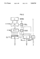
- FIG. 1 is a block circuit diagram of the entire circuit configuration
- FIG. 2 is a block circuit diagram of the structure of a peripheral interrupt node
- FIG. 3 is a schematic circuit diagram of an embodiment of a switching device for a bus connection decision unit inside a peripheral interrupt node;
- FIG. 4 is a schematic and block circuit diagram of the structure of a central activation logic
- FIG. 5 is a block circuit diagram of the structure of a central interrupt node.
- N interrupt sources Q1-QN each being connected through a respective associated peripheral interrupt node PIK1-PIKN to a common interrupt bus IB, which has m signal lines SL.
- the interrupt bus IB also communicates with a central activation logic ZAL and a central interrupt node ZIK, which in turn has access to a central processing unit CPU.
- the central activation logic ZAL is not required if each of the interrupt nodes can directly discharge the m signal lines or if an encoded scheme is used with sets of discharge wires representing a user pre-programmed priority and all lower priorities.
- each peripheral interrupt node PIK having an associated interrupt source Q which presents an interrupt request to the central processing unit CPU activates the signal line SL corresponding to its priority value.
- the central activation logic ZAL thereupon activates the highest-value activated signal line, as well as all of the signal lines having a lower value than that. All of the peripheral interrupt nodes PIK that have not activated the highest-value activated signal line are thereupon precluded from the next selection cycles.
- the central interrupt node ZIK stores the priority value of the highest-value activated signal line SL in memory and combines this priority value with the priority values that were obtained during preceding selection cycles to make a priority number, and compares this number with the priority of the program running at that time in the central processing unit CPU. If the priority number ascertained in this way is accepted by the central processing unit CPU, the peripheral interrupt node PIK having the highest priority number just ascertained can transfer the address of its source to the central processing unit CPU, through the interrupt bus IB.
- the peripheral interrupt node PIK shown in FIG. 2 has a priority register PR, into which the absolute priority number, which may be composed of a level number and a group number, and is associated with the interrupt source Q, can be written.
- the multiplexer MUX is informed through a cycle control circuit ZS as to which portion of the priority number should be transferred from the priority register PR to the decoder.
- a release circuit FS which communicates with the bus connection decision unit BE, releases the output of the decoder DEC whenever the bus connection decision unit BE in the preceding selection cycle had activated the highest-value activated signal line SL. Otherwise, the decoder DEC cannot activate any signal line in the selection cycle just completed, unless it is the first selection cycle being performed, in which all of the peripheral interrupt nodes PIK having interrupt sources Q which have made an interrupt request, can still participate.
- the peripheral interrupt node PIK which is controlled through the cycle control circuit ZS and the release circuit FS, can transmit the vector address assigned to it either by hard wiring or through a register, through a bus connection unit VEC, to the interrupt bus IB.
- the peripheral interrupt node PIK recognizes the acknowledgement signal from the central interrupt node ZIK through a recognition circuit LIA (erase interrupt request), which is likewise activated through the cycle control circuit ZS and the release circuit FS, and as a result informs the associated interrupt source that the interrupt request has been accepted, and that the request should accordingly be erased.
- LIA rase interrupt request
- a three-bit (2 to 1) multiplexer which reads three bits at a time from a six-bit priority register PR during two selection cycles, and through a 1 of 7 decoder DEC activates one of seven signal lines SL.
- the switching example for a bus connection decision unit BE shown in FIG. 3 has seven decoder outputs D0-D6, seven signal lines SL0-SL6, and one output line over which the release circuit FS is informed as to whether or not the peripheral interrupt node (PIK) can again participate in the next selection cycle.
- the interrupt bus IB in this case is formed of seven lines SL0-SL6. At the beginning of each cycle, the bus is preset to the HIGH state. An activation of one signal line then means an resetting of the line to the LOW state.
- Each decoder output D0-D6 controls a transistor T0-T6 and a further transistor T10-T76 in such a way that when the corresponding decoder output D becomes active, the associated signal line SL is reset and the next-higher-value signal line SL is connected to the release circuit FS. If this next-higher signal line SL is reset, that means that this peripheral interrupt node PIK no longer participates during the next selection cycle, because the priority number of its interrupt source Q is lower than the priority number of some other interrupt source Q.
- the central activation logic ZAL is formed of seven level recognition circuits PE0-PE6, which activate their associate and accordingly lower-value signal lines through NAND gates and resetting transistors ET0-ET6.
- the activation of the signal line that is assigned to the particular level recognition circuit itself is performed in order to optimize the level transition speed. Whenever one of the level recognition circuits PE recognizes a change in level of the signal line SL associated with it during one selection cycle, this line and all of the lower-value signal lines SL are connected to ground through the NAND gates and the resetting transistors ET. With the aid of this configuration, it is assured that the bus connection decision units will function correctly even if two interrupt sources Q activate two non-adjacent signal lines SL of the interrupt bus IB.
- the interrupt source Q having the highest priority number recognizes through its bus connection decision unit BE that it has won, and thereupon in turn transmits a vector through the interrupt bus IB to the central processing unit CPU.
- the central interrupt node ZIK has the task of comparing the priority number of the winning interrupt source Q after n selection cycles with the priority of the central processing unit CPU, and of transmitting the received vector to the central processing unit if the new priority is higher, in such a way that the CPU will branch to the appropriate handling routine.
- An acknowledgement signal for erasing the interrupt request of the interrupt node PIK that had won the prioritizing round is transmitted from an acknowledgement signal driver QSTR shown in FIG. 5, through the interrupt bus IB.
- the central interrupt node ZIK is, for instance, formed of a priority encoder COD, which is connected to the interrupt bus IB and sends the number of the signal line SL, encoded, on to a demultiplexer DMUX and a priority latch PRL.
- the priority latch PRL the priority values of the individual selection cycles are combined sequentially to make the complete priority number.
- the demultiplexer DMUX and the priority latch PRL are controlled by a cycle control circuit ZZS, which is activated by the system clock CLK, like the release circuit FS of the peripheral interrupt node PIK.
- a comparator COM compares the priority number stored in memory in the priority latch PRL with the priority number from a processor status word PSW of the program that is being run in the central processing unit CPU.
- the vector address transmitted from the peripheral interrupt node PIK is passed onto the CPU, which thereupon interrupts the program then running and branches to the appropriate interrupt handling routine.
- the central interrupt node ZIK sends an acknowledgement signal through the interrupt bus IB, which causes the interrupt node PIK that has won the prioritizing round to erase the interrupt request at the source connected to it.
- the priority encoder COD is, for instance, in the form of a 7 to 3 encoder
- the demultiplexer DMUX is in the form of a three-bit (1 to 2) circuit.
- the priority registers of the individual peripheral interrupt nodes PIK have a length of six bits, for instance, the priority latch PRL can have a lesser bit width, such as four bits.
- the absolute priority number of an interrupt source is divided into a four-bit level number and a two-bit group number. The level number decides whether or not an interrupt request has a sufficiently high priority to interrupt the running program. In contrast, when a plurality of interrupt requests of the same level number are present, the group number determines which request will be serviced first. Therefore, in this example, only the ascertained four-bit priority level number is compared with the four-bit level number stored in memory in the PSW.
- the central interrupt node ZIK passes the received vector, which in the exemplary embodiment is a six-bit address (each of the 64 possible peripheral interrupt nodes in this system having its own vector), through a vector driver VTR to the CPU. In the next cycle, the acknowledgement signal is transmitted over the interrupt bus IB.
- the CPU itself with a peripheral interrupt node.
- the priority number contained in the PSW must be augmented by a group number.
- the CPU then participates, with the priority assigned to it, in the prioritizing round like every other peripheral interrupt node PIK.
- the central interrupt node then only has the task of receiving the vector and passing it on to the CPU and of generating the acknowledgement signal.
- the CPU accepts the vector only whenever it ascertains that its priority has lost in favor of other priorities during the prioritizing round. It must inform the central interrupt node of this fact, in such a way that the central interrupt node can release the acknowledgement signal from the acknowledgement signal driver QSTR to the interrupt bus IB.
- interrupt bus IB that has 7 signal lines SL
Abstract
Description
Claims (11)
Priority Applications (1)
| Application Number | Priority Date | Filing Date | Title |
|---|---|---|---|
| US07/870,764 US5218703A (en) | 1988-07-07 | 1992-04-20 | Circuit configuration and method for priority selection of interrupts for a microprocessor |
Applications Claiming Priority (4)
| Application Number | Priority Date | Filing Date | Title |
|---|---|---|---|
| DE3823059 | 1988-07-07 | ||
| DE3823059 | 1988-07-07 | ||
| US37684689A | 1989-07-07 | 1989-07-07 | |
| US07/870,764 US5218703A (en) | 1988-07-07 | 1992-04-20 | Circuit configuration and method for priority selection of interrupts for a microprocessor |
Related Parent Applications (1)
| Application Number | Title | Priority Date | Filing Date |
|---|---|---|---|
| US37684689A Continuation | 1988-07-07 | 1989-07-07 |
Publications (1)
| Publication Number | Publication Date |
|---|---|
| US5218703A true US5218703A (en) | 1993-06-08 |
Family
ID=27197894
Family Applications (1)
| Application Number | Title | Priority Date | Filing Date |
|---|---|---|---|
| US07/870,764 Expired - Lifetime US5218703A (en) | 1988-07-07 | 1992-04-20 | Circuit configuration and method for priority selection of interrupts for a microprocessor |
Country Status (1)
| Country | Link |
|---|---|
| US (1) | US5218703A (en) |
Cited By (37)
| Publication number | Priority date | Publication date | Assignee | Title |
|---|---|---|---|---|
| US5404556A (en) * | 1992-06-15 | 1995-04-04 | California Institute Of Technology | Apparatus for carrying out asynchronous communication among integrated circuits |
| US5517624A (en) * | 1992-10-02 | 1996-05-14 | Compaq Computer Corporation | Multiplexed communication protocol between central and distributed peripherals in multiprocessor computer systems |
| US5535420A (en) * | 1994-12-14 | 1996-07-09 | Intel Corporation | Method and apparatus for interrupt signaling in a computer system |
| US5535396A (en) * | 1991-07-06 | 1996-07-09 | Motorola, Inc. | Modulator data/control equipment |
| US5546544A (en) * | 1991-12-04 | 1996-08-13 | North American Philips Corporation | Arbiter with a direct signal path that is modifiable under priority-conflict control |
| US5555420A (en) * | 1990-12-21 | 1996-09-10 | Intel Corporation | Multiprocessor programmable interrupt controller system with separate interrupt bus and bus retry management |
| US5568649A (en) * | 1994-05-31 | 1996-10-22 | Advanced Micro Devices | Interrupt cascading and priority configuration for a symmetrical multiprocessing system |
| US5581771A (en) * | 1993-10-08 | 1996-12-03 | Nec Corporation | Microcomputer having interrupt control circuit to determine priority level |
| US5613128A (en) * | 1990-12-21 | 1997-03-18 | Intel Corporation | Programmable multi-processor interrupt controller system with a processor integrated local interrupt controller |
| US5613126A (en) * | 1994-05-31 | 1997-03-18 | Advanced Micro Devices, Inc. | Timer tick auto-chaining technique within a symmetrical multiprocessing system |
| US5615375A (en) * | 1992-11-17 | 1997-03-25 | Fujitsu Limited | Interrupt control circuit |
| US5619705A (en) * | 1993-12-16 | 1997-04-08 | Intel Corporation | System and method for cascading multiple programmable interrupt controllers utilizing separate bus for broadcasting interrupt request data packet in a multi-processor system |
| US5708813A (en) * | 1994-12-12 | 1998-01-13 | Digital Equipment Corporation | Programmable interrupt signal router |
| US5781187A (en) * | 1994-05-31 | 1998-07-14 | Advanced Micro Devices, Inc. | Interrupt transmission via specialized bus cycle within a symmetrical multiprocessing system |
| US5862366A (en) * | 1996-09-12 | 1999-01-19 | Advanced Micro Devices, Inc. | System and method for simulating a multiprocessor environment for testing a multiprocessing interrupt controller |
| WO1999014679A1 (en) * | 1997-09-12 | 1999-03-25 | Siemens Microelectronics, Inc. | Interrupt system |
| US5894577A (en) * | 1993-09-22 | 1999-04-13 | Advanced Micro Devices, Inc. | Interrupt controller with external in-service indication for power management within a computer system |
| US6205508B1 (en) | 1999-02-16 | 2001-03-20 | Advanced Micro Devices, Inc. | Method for distributing interrupts in a multi-processor system |
| US6295573B1 (en) | 1999-02-16 | 2001-09-25 | Advanced Micro Devices, Inc. | Point-to-point interrupt messaging within a multiprocessing computer system |
| US6389526B1 (en) | 1999-08-24 | 2002-05-14 | Advanced Micro Devices, Inc. | Circuit and method for selectively stalling interrupt requests initiated by devices coupled to a multiprocessor system |
| US6633941B2 (en) | 1999-09-30 | 2003-10-14 | Intel Corporation | Reduced networking interrupts |
| US20040023406A1 (en) * | 2002-07-09 | 2004-02-05 | Schomacker Kevin T. | Optimal windows for obtaining optical data for characterization of tissue samples |
| US6725309B1 (en) * | 1999-03-03 | 2004-04-20 | Hyundai Electronics Industries Co., Ltd. | Multistage interrupt controller for receiving a plurality of interrupt signals to generate a priority interrupt signal |
| US6816934B2 (en) | 2000-12-22 | 2004-11-09 | Hewlett-Packard Development Company, L.P. | Computer system with registered peripheral component interconnect device for processing extended commands and attributes according to a registered peripheral component interconnect protocol |
| US20050193157A1 (en) * | 2004-02-27 | 2005-09-01 | Min-Do Kwon | Apparatus and method for interrupt source signal allocation |
| US20050223149A1 (en) * | 2004-03-30 | 2005-10-06 | Nec Electronics Corporation | Interrupt controlling circuit |
| US20050257224A1 (en) * | 2004-04-28 | 2005-11-17 | Whalen Shaun P | Processor with instruction-based interrupt handling |
| US20070288895A1 (en) * | 2006-06-08 | 2007-12-13 | Sun Microsystems, Inc. | Configuration tool with multi-level priority semantic |
| US20090070546A1 (en) * | 2007-09-11 | 2009-03-12 | Shubhodeep Roy Choudhury | System and Method for Generating Fast Instruction and Data Interrupts for Processor Design Verification and Validation |
| US20090070570A1 (en) * | 2007-09-11 | 2009-03-12 | Shubhodeep Roy Choudhury | System and Method for Efficiently Handling Interrupts |
| US20090070532A1 (en) * | 2007-09-11 | 2009-03-12 | Vinod Bussa | System and Method for Efficiently Testing Cache Congruence Classes During Processor Design Verification and Validation |
| US20100217906A1 (en) * | 2009-02-20 | 2010-08-26 | Qualcomm Incorporated | Methods And Aparatus For Resource Sharing In A Programmable Interrupt Controller |
| US7992059B2 (en) | 2007-09-11 | 2011-08-02 | International Business Machines Corporation | System and method for testing a large memory area during processor design verification and validation |
| US8006221B2 (en) | 2007-09-11 | 2011-08-23 | International Business Machines Corporation | System and method for testing multiple processor modes for processor design verification and validation |
| US8145467B1 (en) * | 2008-02-25 | 2012-03-27 | Xilinx, Inc. | Method and apparatus for profiling a hardware/software embedded system |
| US10684965B2 (en) | 2017-11-08 | 2020-06-16 | Advanced Micro Devices, Inc. | Method to reduce write responses to improve bandwidth and efficiency |
| CN116185915A (en) * | 2023-04-21 | 2023-05-30 | 山东云海国创云计算装备产业创新中心有限公司 | Bus scheduling method, device and equipment, medium and baseboard management control chip |
Citations (13)
| Publication number | Priority date | Publication date | Assignee | Title |
|---|---|---|---|---|
| US4172284A (en) * | 1976-12-30 | 1979-10-23 | International Business Machines Corporation | Priority interrupt apparatus employing a plural stage shift register having separate interrupt mechanisms coupled to the different stages thereof for segregating interrupt requests according to priority levels |
| US4218739A (en) * | 1976-10-28 | 1980-08-19 | Honeywell Information Systems Inc. | Data processing interrupt apparatus having selective suppression control |
| US4275458A (en) * | 1979-12-14 | 1981-06-23 | Gte Automatic Electric Laboratories Incorporated | Interrupt expander circuit |
| US4349873A (en) * | 1980-04-02 | 1982-09-14 | Motorola, Inc. | Microprocessor interrupt processing |
| US4470111A (en) * | 1979-10-01 | 1984-09-04 | Ncr Corporation | Priority interrupt controller |
| US4484302A (en) * | 1980-11-20 | 1984-11-20 | International Business Machines Corporation | Single screen display system with multiple virtual display having prioritized service programs and dedicated memory stacks |
| US4536839A (en) * | 1982-03-30 | 1985-08-20 | Mai Basic Four, Inc. | Memory request arbitrator |
| US4621342A (en) * | 1983-02-03 | 1986-11-04 | Cselt Centro Studi E Laboratori Telecomunicazioni S.P.A. | Arbitration circuitry for deciding access requests from a multiplicity of components |
| US4648029A (en) * | 1984-08-27 | 1987-03-03 | International Business Machines Corporation | Multiplexed interrupt/DMA request arbitration apparatus and method |
| US4764869A (en) * | 1985-08-30 | 1988-08-16 | Hitachi, Ltd. | Method and apparatus for controlling interruption in the course of instruction execution in a processor |
| US4791553A (en) * | 1981-10-20 | 1988-12-13 | Italtel-Societa Italiana Telecomunicazioni S.P.A. | Control unit of input-output interface circuits in an electronic processor |
| US4868742A (en) * | 1984-06-20 | 1989-09-19 | Convex Computer Corporation | Input/output bus for system which generates a new header parcel when an interrupted data block transfer between a computer and peripherals is resumed |
| US4920486A (en) * | 1987-11-23 | 1990-04-24 | Digital Equipment Corporation | Distributed arbitration apparatus and method for shared bus |
-
1992
- 1992-04-20 US US07/870,764 patent/US5218703A/en not_active Expired - Lifetime
Patent Citations (13)
| Publication number | Priority date | Publication date | Assignee | Title |
|---|---|---|---|---|
| US4218739A (en) * | 1976-10-28 | 1980-08-19 | Honeywell Information Systems Inc. | Data processing interrupt apparatus having selective suppression control |
| US4172284A (en) * | 1976-12-30 | 1979-10-23 | International Business Machines Corporation | Priority interrupt apparatus employing a plural stage shift register having separate interrupt mechanisms coupled to the different stages thereof for segregating interrupt requests according to priority levels |
| US4470111A (en) * | 1979-10-01 | 1984-09-04 | Ncr Corporation | Priority interrupt controller |
| US4275458A (en) * | 1979-12-14 | 1981-06-23 | Gte Automatic Electric Laboratories Incorporated | Interrupt expander circuit |
| US4349873A (en) * | 1980-04-02 | 1982-09-14 | Motorola, Inc. | Microprocessor interrupt processing |
| US4484302A (en) * | 1980-11-20 | 1984-11-20 | International Business Machines Corporation | Single screen display system with multiple virtual display having prioritized service programs and dedicated memory stacks |
| US4791553A (en) * | 1981-10-20 | 1988-12-13 | Italtel-Societa Italiana Telecomunicazioni S.P.A. | Control unit of input-output interface circuits in an electronic processor |
| US4536839A (en) * | 1982-03-30 | 1985-08-20 | Mai Basic Four, Inc. | Memory request arbitrator |
| US4621342A (en) * | 1983-02-03 | 1986-11-04 | Cselt Centro Studi E Laboratori Telecomunicazioni S.P.A. | Arbitration circuitry for deciding access requests from a multiplicity of components |
| US4868742A (en) * | 1984-06-20 | 1989-09-19 | Convex Computer Corporation | Input/output bus for system which generates a new header parcel when an interrupted data block transfer between a computer and peripherals is resumed |
| US4648029A (en) * | 1984-08-27 | 1987-03-03 | International Business Machines Corporation | Multiplexed interrupt/DMA request arbitration apparatus and method |
| US4764869A (en) * | 1985-08-30 | 1988-08-16 | Hitachi, Ltd. | Method and apparatus for controlling interruption in the course of instruction execution in a processor |
| US4920486A (en) * | 1987-11-23 | 1990-04-24 | Digital Equipment Corporation | Distributed arbitration apparatus and method for shared bus |
Cited By (55)
| Publication number | Priority date | Publication date | Assignee | Title |
|---|---|---|---|---|
| US5701496A (en) * | 1990-12-21 | 1997-12-23 | Intel Corporation | Multi-processor computer system with interrupt controllers providing remote reading |
| US5613128A (en) * | 1990-12-21 | 1997-03-18 | Intel Corporation | Programmable multi-processor interrupt controller system with a processor integrated local interrupt controller |
| US5555420A (en) * | 1990-12-21 | 1996-09-10 | Intel Corporation | Multiprocessor programmable interrupt controller system with separate interrupt bus and bus retry management |
| US5696976A (en) * | 1990-12-21 | 1997-12-09 | Intel Corporation | Protocol for interrupt bus arbitration in a multi-processor system |
| US5535396A (en) * | 1991-07-06 | 1996-07-09 | Motorola, Inc. | Modulator data/control equipment |
| US5546544A (en) * | 1991-12-04 | 1996-08-13 | North American Philips Corporation | Arbiter with a direct signal path that is modifiable under priority-conflict control |
| US5404556A (en) * | 1992-06-15 | 1995-04-04 | California Institute Of Technology | Apparatus for carrying out asynchronous communication among integrated circuits |
| US5517624A (en) * | 1992-10-02 | 1996-05-14 | Compaq Computer Corporation | Multiplexed communication protocol between central and distributed peripherals in multiprocessor computer systems |
| US5615375A (en) * | 1992-11-17 | 1997-03-25 | Fujitsu Limited | Interrupt control circuit |
| US5894577A (en) * | 1993-09-22 | 1999-04-13 | Advanced Micro Devices, Inc. | Interrupt controller with external in-service indication for power management within a computer system |
| US5581771A (en) * | 1993-10-08 | 1996-12-03 | Nec Corporation | Microcomputer having interrupt control circuit to determine priority level |
| US5619705A (en) * | 1993-12-16 | 1997-04-08 | Intel Corporation | System and method for cascading multiple programmable interrupt controllers utilizing separate bus for broadcasting interrupt request data packet in a multi-processor system |
| US5781187A (en) * | 1994-05-31 | 1998-07-14 | Advanced Micro Devices, Inc. | Interrupt transmission via specialized bus cycle within a symmetrical multiprocessing system |
| US5613126A (en) * | 1994-05-31 | 1997-03-18 | Advanced Micro Devices, Inc. | Timer tick auto-chaining technique within a symmetrical multiprocessing system |
| US5568649A (en) * | 1994-05-31 | 1996-10-22 | Advanced Micro Devices | Interrupt cascading and priority configuration for a symmetrical multiprocessing system |
| US5708813A (en) * | 1994-12-12 | 1998-01-13 | Digital Equipment Corporation | Programmable interrupt signal router |
| US5535420A (en) * | 1994-12-14 | 1996-07-09 | Intel Corporation | Method and apparatus for interrupt signaling in a computer system |
| US5862366A (en) * | 1996-09-12 | 1999-01-19 | Advanced Micro Devices, Inc. | System and method for simulating a multiprocessor environment for testing a multiprocessing interrupt controller |
| US5968159A (en) * | 1997-09-12 | 1999-10-19 | Infineon Technologies Corporation | Interrupt system with fast response time |
| WO1999014679A1 (en) * | 1997-09-12 | 1999-03-25 | Siemens Microelectronics, Inc. | Interrupt system |
| US20060031621A1 (en) * | 1998-09-03 | 2006-02-09 | Compaq Computer Corporation | High speed peripheral interconnect apparatus, method and system |
| US20050273534A1 (en) * | 1998-09-03 | 2005-12-08 | Compaq Computer Corporation | High speed peripheral interconnect apparatus, method and system |
| US20050033893A1 (en) * | 1998-09-03 | 2005-02-10 | Compaq Computer Corporation | High speed peripheral interconnect apparatus, method and system |
| US7587542B2 (en) | 1998-09-03 | 2009-09-08 | Hewlett-Packard Development Company, L.P. | Device adapted to send information in accordance with a communication protocol |
| US7464207B2 (en) | 1998-09-03 | 2008-12-09 | Hewlett-Packard Development Company, L.P. | Device operating according to a communication protocol |
| US7099986B2 (en) | 1998-09-03 | 2006-08-29 | Hewlett-Packard Development Company, L.P. | High speed peripheral interconnect apparatus, method and system |
| US6295573B1 (en) | 1999-02-16 | 2001-09-25 | Advanced Micro Devices, Inc. | Point-to-point interrupt messaging within a multiprocessing computer system |
| US6205508B1 (en) | 1999-02-16 | 2001-03-20 | Advanced Micro Devices, Inc. | Method for distributing interrupts in a multi-processor system |
| US6725309B1 (en) * | 1999-03-03 | 2004-04-20 | Hyundai Electronics Industries Co., Ltd. | Multistage interrupt controller for receiving a plurality of interrupt signals to generate a priority interrupt signal |
| US6389526B1 (en) | 1999-08-24 | 2002-05-14 | Advanced Micro Devices, Inc. | Circuit and method for selectively stalling interrupt requests initiated by devices coupled to a multiprocessor system |
| US6760799B1 (en) * | 1999-09-30 | 2004-07-06 | Intel Corporation | Reduced networking interrupts |
| US6633941B2 (en) | 1999-09-30 | 2003-10-14 | Intel Corporation | Reduced networking interrupts |
| US6816934B2 (en) | 2000-12-22 | 2004-11-09 | Hewlett-Packard Development Company, L.P. | Computer system with registered peripheral component interconnect device for processing extended commands and attributes according to a registered peripheral component interconnect protocol |
| US20040023406A1 (en) * | 2002-07-09 | 2004-02-05 | Schomacker Kevin T. | Optimal windows for obtaining optical data for characterization of tissue samples |
| US20050193157A1 (en) * | 2004-02-27 | 2005-09-01 | Min-Do Kwon | Apparatus and method for interrupt source signal allocation |
| US7484024B2 (en) * | 2004-02-27 | 2009-01-27 | Samsung Electronics Co., Ltd | Apparatus and method for interrupt source signal allocation |
| US20050223149A1 (en) * | 2004-03-30 | 2005-10-06 | Nec Electronics Corporation | Interrupt controlling circuit |
| US7308518B2 (en) * | 2004-03-30 | 2007-12-11 | Nec Electronics Corporation | Interrupt controlling circuit |
| US20050257224A1 (en) * | 2004-04-28 | 2005-11-17 | Whalen Shaun P | Processor with instruction-based interrupt handling |
| US7831979B2 (en) * | 2004-04-28 | 2010-11-09 | Agere Systems Inc. | Processor with instruction-based interrupt handling |
| US20070288895A1 (en) * | 2006-06-08 | 2007-12-13 | Sun Microsystems, Inc. | Configuration tool with multi-level priority semantic |
| US7831960B2 (en) * | 2006-06-08 | 2010-11-09 | Oracle America, Inc. | Configuration tool with multi-level priority semantic |
| US8099559B2 (en) | 2007-09-11 | 2012-01-17 | International Business Machines Corporation | System and method for generating fast instruction and data interrupts for processor design verification and validation |
| US20090070532A1 (en) * | 2007-09-11 | 2009-03-12 | Vinod Bussa | System and Method for Efficiently Testing Cache Congruence Classes During Processor Design Verification and Validation |
| US20090070570A1 (en) * | 2007-09-11 | 2009-03-12 | Shubhodeep Roy Choudhury | System and Method for Efficiently Handling Interrupts |
| US7992059B2 (en) | 2007-09-11 | 2011-08-02 | International Business Machines Corporation | System and method for testing a large memory area during processor design verification and validation |
| US8006221B2 (en) | 2007-09-11 | 2011-08-23 | International Business Machines Corporation | System and method for testing multiple processor modes for processor design verification and validation |
| US8019566B2 (en) | 2007-09-11 | 2011-09-13 | International Business Machines Corporation | System and method for efficiently testing cache congruence classes during processor design verification and validation |
| US20090070546A1 (en) * | 2007-09-11 | 2009-03-12 | Shubhodeep Roy Choudhury | System and Method for Generating Fast Instruction and Data Interrupts for Processor Design Verification and Validation |
| US8145467B1 (en) * | 2008-02-25 | 2012-03-27 | Xilinx, Inc. | Method and apparatus for profiling a hardware/software embedded system |
| US20100217906A1 (en) * | 2009-02-20 | 2010-08-26 | Qualcomm Incorporated | Methods And Aparatus For Resource Sharing In A Programmable Interrupt Controller |
| US8244947B2 (en) * | 2009-02-20 | 2012-08-14 | Qualcomm Incorporated | Methods and apparatus for resource sharing in a programmable interrupt controller |
| US10684965B2 (en) | 2017-11-08 | 2020-06-16 | Advanced Micro Devices, Inc. | Method to reduce write responses to improve bandwidth and efficiency |
| CN116185915A (en) * | 2023-04-21 | 2023-05-30 | 山东云海国创云计算装备产业创新中心有限公司 | Bus scheduling method, device and equipment, medium and baseboard management control chip |
| CN116185915B (en) * | 2023-04-21 | 2023-08-04 | 山东云海国创云计算装备产业创新中心有限公司 | Bus scheduling method, device and equipment, medium and baseboard management control chip |
Similar Documents
| Publication | Publication Date | Title |
|---|---|---|
| US5218703A (en) | Circuit configuration and method for priority selection of interrupts for a microprocessor | |
| US4130864A (en) | Priority selection circuit for multiported central functional unit with automatic priority reduction on excessive port request | |
| US4621342A (en) | Arbitration circuitry for deciding access requests from a multiplicity of components | |
| US5805922A (en) | Queued serial peripheral interface having multiple queues for use in a data processing system | |
| US4519028A (en) | CPU with multi-stage mode register for defining CPU operating environment including charging its communications protocol | |
| US4023143A (en) | Fixed priority interrupt control circuit | |
| US3983540A (en) | Rapid bus priority resolution | |
| US4463445A (en) | Circuitry for allocating access to a demand-shared bus | |
| US4451881A (en) | Data processing system bus for multiple independent users | |
| US5101497A (en) | Programmable interrupt controller | |
| US5027348A (en) | Method and apparatus for dynamic data block length adjustment | |
| US5237567A (en) | Processor communication bus | |
| US6647449B1 (en) | System, method and circuit for performing round robin arbitration | |
| US4675812A (en) | Priority circuit for channel subsystem having components with diverse and changing requirement for system resources | |
| US6182165B1 (en) | Staggered polling of buffer descriptors in a buffer descriptor ring direct memory access system | |
| EP0535821A1 (en) | Method and apparatus for dynamically steering undirected interrupts | |
| US5603035A (en) | Programmable interrupt controller, interrupt system and interrupt control process | |
| EP0327203B1 (en) | NxM arbitrating non-blocking high bandwidth switch | |
| EP0106879B1 (en) | Method and apparatus for limiting bus utilization | |
| WO1999060488A1 (en) | Software configurable technique for prioritizing interrupts in a microprocessor-based system | |
| JPS6142306B2 (en) | ||
| US5371893A (en) | Look-ahead priority arbitration system and method | |
| EP0435092B1 (en) | Data processing system with direct memory access controller and method for varying communication bus masterchip in response to prioritized interrupt requests | |
| US4788639A (en) | Frequency-coded multi-level interrupt control system for a multiprocessor system | |
| US7093045B2 (en) | Method and apparatus for bus arbitration capable of effectively altering a priority order |
Legal Events
| Date | Code | Title | Description |
|---|---|---|---|
| AS | Assignment |
Owner name: SIEMENS AKTIENGESELLSCHAFT, GERMANY Free format text: ASSIGNMENT OF ASSIGNORS INTEREST.;ASSIGNORS:FLECK, ROD;PORET, MARK;MATTHEIS, KARL-HEINZ;REEL/FRAME:006420/0923;SIGNING DATES FROM 19890727 TO 19890808 |
|
| STCF | Information on status: patent grant |
Free format text: PATENTED CASE |
|
| FEPP | Fee payment procedure |
Free format text: PAYOR NUMBER ASSIGNED (ORIGINAL EVENT CODE: ASPN); ENTITY STATUS OF PATENT OWNER: LARGE ENTITY |
|
| FPAY | Fee payment |
Year of fee payment: 4 |
|
| FPAY | Fee payment |
Year of fee payment: 8 |
|
| FEPP | Fee payment procedure |
Free format text: PAYER NUMBER DE-ASSIGNED (ORIGINAL EVENT CODE: RMPN); ENTITY STATUS OF PATENT OWNER: LARGE ENTITY Free format text: PAYOR NUMBER ASSIGNED (ORIGINAL EVENT CODE: ASPN); ENTITY STATUS OF PATENT OWNER: LARGE ENTITY |
|
| FPAY | Fee payment |
Year of fee payment: 12 |
|
| AS | Assignment |
Owner name: INFINEON TECHNOLOGIES AG, GERMANY Free format text: ASSIGNMENT OF ASSIGNORS INTEREST;ASSIGNOR:SIEMENS AKTIENGESELLSCHAFT;REEL/FRAME:026358/0703 Effective date: 19990331 |