US5378945A - Voltage level converting buffer circuit - Google Patents
Voltage level converting buffer circuit Download PDFInfo
- Publication number
- US5378945A US5378945A US08/097,781 US9778193A US5378945A US 5378945 A US5378945 A US 5378945A US 9778193 A US9778193 A US 9778193A US 5378945 A US5378945 A US 5378945A
- Authority
- US
- United States
- Prior art keywords
- transistor
- buffer circuit
- voltage level
- source
- gate
- Prior art date
- Legal status (The legal status is an assumption and is not a legal conclusion. Google has not performed a legal analysis and makes no representation as to the accuracy of the status listed.)
- Expired - Lifetime
Links
Images
Classifications
-
- H—ELECTRICITY
- H03—ELECTRONIC CIRCUITRY
- H03K—PULSE TECHNIQUE
- H03K19/00—Logic circuits, i.e. having at least two inputs acting on one output; Inverting circuits
- H03K19/003—Modifications for increasing the reliability for protection
- H03K19/00315—Modifications for increasing the reliability for protection in field-effect transistor circuits
-
- H—ELECTRICITY
- H03—ELECTRONIC CIRCUITRY
- H03K—PULSE TECHNIQUE
- H03K19/00—Logic circuits, i.e. having at least two inputs acting on one output; Inverting circuits
- H03K19/0175—Coupling arrangements; Interface arrangements
- H03K19/0185—Coupling arrangements; Interface arrangements using field effect transistors only
- H03K19/018507—Interface arrangements
- H03K19/018521—Interface arrangements of complementary type, e.g. CMOS
Definitions
- This invention relates generally to voltage level conversion buffers for integrated circuit components, and more particularly to a buffer circuit which converts a logic signal at a first voltage level to a logic signal at a second different voltage level.
- MOSFET metal-oxide-semiconductor field-effect transistors
- a MOSFET generally includes a source and a drain each coupled to an n-type (or p-type) region having a p-type (or n-type) channel between the two regions and a gate coupled to a dielectric layer used to isolate the gate from the channel.
- a voltage applied to the gate induces an electric field across the gate dielectric layer and modulates the free-carrier concentration in the channel region.
- MOSFETs are generally small and easy to fabricate, and significant improvements in switching speed and power consumption can be made if complementary-symmetry MOSFETs (i.e., CMOS devices; both NMOS and PMOS devices) are used.
- One technique used to reduce power consumption is to reduce the supply voltage provided to the transistors in the IC. Additionally, as the transistors become smaller, a reduced supply voltage may also be required to lower the electric fields across the transistor terminals which can cause various reliability problems.
- transistors which are capable of conducting a maximum current flow equal to the maximum current flow through transistors using a higher supply voltage such that transistors using a reduced supply voltage level will have comparable switching times to transistors using a higher supply voltage level.
- the gate dielectric will irreparably break down and permanently change from an insulator to a conductor (i.e., the transistor behaves as a resistive short).
- Vgs is generally kept less than or equal to the supply voltage.
- Vdd the asserted input signal voltage level provided by components using higher supply voltages, Vdd, cannot be directly applied to gates of transistors which must operate at a reduced supply voltage, Vddr.
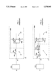
- FIG. 1 One technique used to protect a component using a reduced supply voltage, Vddr, from input signals from a component using a higher supply voltage, Vdd, is shown in FIG. 1.
- a component 10 is shown coupled to an input terminal 12 of a component 14.
- Component 10 uses a supply voltage Vdd while component 14 uses a reduced supply voltage Vddr.
- Input terminal 12 is shown coupled to buffer circuit 16 which includes an NMOS transistor 18 having a drain 18d, a gate 18g, and a source 18s.
- the drain 18d is connected to input terminal 12, the gate 18g is connected to Vddr, and the source 18s is coupled to logic element 20.
- Logic element 20 is shown to include an NMOS transistor 22 and a PMOS transistor 24 connected in such a way as to provide an inverter.
- the source 18s of the NMOS transistor 18 is connected to the gates 22g, 24g of NMOS transistor 22 and PMOS transistor 24, respectively.
- NMOS transistor 22 will be fully conducting when the gate to source voltage drop, Vgs, is equal to Vddr, and PMOS transistor 24 will be fully off when
- the aggregate standby current may be higher than a maximum allowable standby current and may cause significant standby power consumption. This type of component may not be readily usable in a battery powered system.
- FIG. 2 A technique used to reduce the cross-current discussed above is shown in FIG. 2 where the buffer circuit 16 of FIG. 1 is shown with the addition of a PMOS transistor 26 having a gate 26g, a drain 26d, and a source 26s.
- the output of inverter 20 is shown connected to gate 26g, while source 26s is connected to Vddr and drain 26d is connected to the output of buffer circuit 16 and input of inverter 20.
- PMOS transistor 26 is one technique used to increase the voltage level provided to gates 22g, 24g of inverter 20 when the input signal applied to input terminal 12 is asserted.
- the PMOS transistor 24 when an asserted input signal is applied to input terminal 12, initially, the PMOS transistor 24 will not be fully off and the NMOS transistor 22g will not be fully on. However, the output of the inverter will be approximately a low output signal.
- the arrangement of FIG. 2 provides this low output signal to the gate 26g of PMOS transistor 26 which turns transistor 26 on and allows current to flow from source 26s to drain 26d such that the voltage level at drain 26d is increased to Vddr provided that the asserted voltage level applied to input terminal 12 is greater than or equal to Vddr-Vt which will be discussed more fully below. Raising the input voltage level of inverter 20 to Vddr prevents the cross-current discussed above in reference to the circuit of FIG. 1.
- a back-drive current may be generated from PMOS transistor 26 through transistor 18 to input terminal 12.
- the transistor 18 will begin conducting current from source 18s to drain 18d, thus, producing a back-drive current to input terminal 12.
- This back-drive of current will prevent PMOS transistor 26 from pulling up the inverter 20 input to Vddr, and thus, will not eliminate the cross-current discussed in reference to the circuit of FIG. 1. Further, this back-drive current may violate very small limits placed on component input pad leakage.
- a voltage level converting buffer circuit for an integrated circuit component includes a first and a second transistor each having a gate, a drain, and a source.
- the drain of the first transistor and the gate of the second transistor are connected together to receive an input for the buffer circuit, and the gate of the first transistor and the drain of the second transistor are connected to a supply voltage.
- the sources of the first and second transistors are connected together to provide an output for the buffer circuit.
- the buffer circuit converts an asserted input signal voltage level into a maximum allowable asserted input signal voltage level which is sufficient to allow for maximum transistor current conduction within the low-power integrated circuit component transistors while maintaining switching speed and preventing transistor damage, a back-drive current, and a cross-current within the low-power component transistors.
- FIG. 1 is a schematic diagram of a first prior art voltage level converting buffer circuit for an integrated circuit component
- FIG. 2 is a schematic diagram of a second prior art voltage level converting buffer circuit for an integrated circuit component
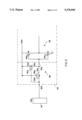
- FIG. 3 is a schematic diagram of a voltage level converting buffer circuit for an integrated circuit component in accordance with the invention.
- a component 30 is shown coupled to an input terminal 32a of a component 34.
- FIG. 3 also shows that component 30 uses a supply voltage Vdd while component 34 uses a reduced supply voltage Vddr.
- Component 34 which can be any suitable logic device is shown to include a buffer circuit 36 having the input terminal 32a, said buffer circuit 36 is provided to convert a signal at a first voltage level from component 30 to a signal at a second voltage level for use in component 34 which uses a reduced supply voltage Vddr.
- Component 34 will generally have many input terminals (not shown) and will generally include an associated number of buffer circuits (not shown).
- input terminal 32a is shown coupled to buffer circuit 36 which includes an NMOS transistor 38 having a drain 38d, a gate 38g, and a source 38s and an NMOS transistor 40 having a drain 40d, a gate 40g, and a source 40s.
- Drain 38d and gate 40g are shown connected to input terminal 32a
- gate 38g and drain 40d are connected to the reduced supply voltage Vddr
- source 38s is connected to source 40s and logic element 42.
- Logic element 42 is shown coupled to buffer circuit output terminal 32b, and includes an NMOS transistor 44 and a PMOS transistor 46 connected in a known way to form an inverter.
- the sources 38s, 40s of the NMOS transistors 38, 40, respectively, are connected to gates 44g, 46g of NMOS transistor 44 and PMOS transistor 46, respectively.
- the logic element 42 is shown as an inverter in FIG. 3, however, it is to be understood that any logic element may be connected to buffer circuit 36.
- the invention includes a voltage level conversion buffer circuit for an integrated circuit (IC) component.
- the IC component will be referred to as a low-power component, because it contains logic elements, for example, inverter 42 as shown in FIG. 3, comprising transistors using a supply voltage, referred to as a reduced supply voltage, which is lower than the voltage level of asserted signals driven as outputs by components to which input terminals of the low-power component are coupled.
- the buffer circuit converts an asserted input signal voltage level into a maximum allowable asserted input signal voltage level. The converted asserted signal is then provided to an input of a logic element comprising transistors using the reduced supply voltage.
- the arrangement depicted in FIG. 3, prevents the gate to source voltage drop (i.e., Vgs) in transistors 44, 46 from being greater than the reduced supply voltage Vddr in order to prevent gate dielectric breakdown and other reliability problems in those transistors.
- the arrangement also provides an asserted signal voltage level related to the input signal voltage level provided at input terminal 32a and limited to Vddr to inverter 42 which will prevent a cross-current between the transistors 44, 46 of inverter 42 when the input signal voltage level is greater than or equal to Vddr+Vt and will prevent a back-drive current through transistor 38.
- component 34 is a CMOS device having Vddr equal to 3.6 V and threshold voltage Vt equal to 0.6 V.
- Component 30 connected to input terminal 32a of component 34 is a different device having Vdd equal to 5 V such that the maximum asserted signal voltage level provided at input terminal 32a by component 30 will be 5 V and the deasserted signal voltage level provided at input terminal 32a will be 0 V.
- drain 38d of transistor 38 and gate 40g of transistor 40 are also deasserted through direct connections to input terminal 32a.
- transistor 38 When the input signal voltage level applied to input terminal 32a changes from being deasserted to being asserted, initially, transistor 38 is on (Vgs>Vt). As input terminal 32a changes from being deasserted to being asserted, the current being conducted through transistor 38 increases the voltage level at source 38s. Thus, the voltage level at the input to inverter 42 is approximately equal to the voltage level of input terminal 32a, Vin, as shown in the table above.
- Transistor 38 prevents gate dielectric breakdown in transistors 44, 46 of inverter 42 by limiting the voltage level provided at gates 44g, 46g to a maximum of Vddr-Vt. However, the voltage limiting provided by transistor 38 alone would cause a cross-current between transistor 46 and transistor 44 when an asserted input signal voltage level is provided at input terminal 32a.
- Transistor 40 will not begin conducting current until Vgs is greater than Vt (i.e., Vin ⁇ Vddr), and because the voltage level at the source 38s of transistor 38 is increasing and is connected to source 40s of transistor 40, Vgs of transistor 40 may not be greater than Vt until the voltage level at input terminal 32a, and hence, gate 40g of transistor 40 is 3.6 V (i.e., Vddr) and rising. At this point, Vgs for transistor 40 is 0.6 V which is equal to Vt and as voltage level of gate 40g rises, transistor 40 will begin conducting current from drain 40d to source 40s. When transistor 40 turns on, the voltage level at source 40s will be increased substantially close to Vddr.
- Vgs of transistor 40 prevents Vgs of transistor 40 from becoming greater than Vddr which prevents gate dielectric breakdown.
- Vddr a critical level
- Vgs of transistor 40 will not reach a level greater than Vddr, because the voltage level provided at source 38s by transistor 38 is approximately 3.0 V and the voltage level provided to gate 40g of transistor 40 is approximately 5.5 V maximum.
- Vgs for transistor 40 is a maximum of approximately 2.5 V which is less than Vddr (i.e., 3.6 V) and thus, far less than the critical voltage level.
- transistor 40 eliminates any cross-current between PMOS transistor 46 and NMOS transistor 44 of inverter 42.
- transistor 40 Since transistor 40 will not increase the voltage level at source 40s to Vddr until the voltage level at input terminal 32a is greater than or equal to Vddr+Vt, the voltage level at source 38s will never be greater than the voltage level provided at input terminal 32a. This prevents a back-drive of current through transistor 38.
- buffer circuit 36 and in particular transistor 38 would provide the TTL asserted and deasserted voltage levels to the input of inverter 42, but buffer circuit 36 and in particular transistor 40 would not increase the voltage level at the input to inverter 42 to Vddr.
- buffer circuit 36 would not eliminate the cross-current in inverter 42, but buffer circuit 36 would substantially prevent a back-drive current through transistor 38 keeping the voltage level at the input to inverter 42 approximately equal to the voltage level applied at input terminal 32a.
- Buffer circuit 36 requires very little space which is generally a critical factor in integrated circuit components. Further, buffer circuit 36 comprises the same type of transistors as the logic elements making up the component, and accordingly, the buffer circuit does not complicate the fabrication process for the component. Additionally, the buffer circuit is readily adaptable for use with different voltages.
Abstract
Description
______________________________________
Input Terminal
             Inverter 20 Input
                          Inverter 42 Input
Voltage Level
             Voltage Level
                          Voltage Level
Vin          (FIG. 1)     (FIG. 3)
______________________________________
0 V → Vddr - Vt
             Vin          Vin
Vddr - Vt → Vddr
             Vddr - Vt    Vddr - Vt
Vddr → Vddr + Vt
             Vddr - Vt    Vin - Vt
≧Vddr + Vt
             Vddr - Vt    Vddr
______________________________________
Claims (9)
Priority Applications (1)
| Application Number | Priority Date | Filing Date | Title |
|---|---|---|---|
| US08/097,781 US5378945A (en) | 1993-07-26 | 1993-07-26 | Voltage level converting buffer circuit |
Applications Claiming Priority (1)
| Application Number | Priority Date | Filing Date | Title |
|---|---|---|---|
| US08/097,781 US5378945A (en) | 1993-07-26 | 1993-07-26 | Voltage level converting buffer circuit |
Publications (1)
| Publication Number | Publication Date |
|---|---|
| US5378945A true US5378945A (en) | 1995-01-03 |
Family
ID=22265098
Family Applications (1)
| Application Number | Title | Priority Date | Filing Date |
|---|---|---|---|
| US08/097,781 Expired - Lifetime US5378945A (en) | 1993-07-26 | 1993-07-26 | Voltage level converting buffer circuit |
Country Status (1)
| Country | Link |
|---|---|
| US (1) | US5378945A (en) |
Cited By (14)
| Publication number | Priority date | Publication date | Assignee | Title |
|---|---|---|---|---|
| EP0690578A1 (en) * | 1994-05-31 | 1996-01-03 | Nec Corporation | MOSFET interface circuit having an increased or a reduced mutual conductance |
| US5541534A (en) * | 1995-02-13 | 1996-07-30 | International Business Machines Corporation | Mixed voltage interface converter |
| US5661416A (en) * | 1994-05-02 | 1997-08-26 | Hitachi, Ltd. | Interface circuit and interface-network system using the same |
| US5748028A (en) * | 1996-10-31 | 1998-05-05 | International Business Machines Corporation | Method and apparatus for multi-level input voltage receiver circuit |
| EP0865163A1 (en) * | 1997-03-14 | 1998-09-16 | Lucent Technologies Inc. | High-voltage tolerant input buffer in low-voltage technology |
| WO2003069780A1 (en) * | 2002-02-11 | 2003-08-21 | Honeywell International Inc. | Multi power supply circuit protection apparatus and method |
| US20040032284A1 (en) * | 2002-06-13 | 2004-02-19 | Stmicroelectronics Pvt. Ltd. | Digital electronic circuit for translating high voltage levels to low voltage levels |
| US20050110520A1 (en) * | 2003-11-20 | 2005-05-26 | Industrial Technology Research Institute. | Input stage for mixed-voltage-tolerant buffer without leakage issue |
| KR100549935B1 (en) * | 1998-12-08 | 2006-05-03 | 삼성전자주식회사 | Input buffer of semiconductor memory device |
| KR100631909B1 (en) * | 1999-12-13 | 2006-10-04 | 삼성전자주식회사 | Buffer circuit |
| US8044684B1 (en) | 2010-04-15 | 2011-10-25 | Stmicroelectronics Pvt. Ltd. | Input and output buffer including a dynamic driver reference generator |
| WO2014110371A1 (en) * | 2013-01-14 | 2014-07-17 | Qualcomm Incorporated | Single-ended high voltage input-capable comparator circuit |
| US9536593B1 (en) * | 2016-05-23 | 2017-01-03 | Qualcomm Incorporated | Low power receiver with wide input voltage range |
| US10924093B1 (en) * | 2019-10-31 | 2021-02-16 | Nxp Usa, Inc. | Integrated circuit with finFETs having dummy structures |
Citations (4)
| Publication number | Priority date | Publication date | Assignee | Title |
|---|---|---|---|---|
| US4935649A (en) * | 1988-07-11 | 1990-06-19 | Cypress Semiconductor Corporation | Clamped sense amplifier |
| US4963765A (en) * | 1989-07-03 | 1990-10-16 | Texas Instruments Incorporated | High speed CMOS transition detector circuit |
| US5057712A (en) * | 1989-09-29 | 1991-10-15 | Advanced Micro Device, Inc. | Address transition detector for programmable logic array |
| US5151616A (en) * | 1990-01-23 | 1992-09-29 | Nec Corporation | Cmos high voltage switch |
-
1993
- 1993-07-26 US US08/097,781 patent/US5378945A/en not_active Expired - Lifetime
Patent Citations (4)
| Publication number | Priority date | Publication date | Assignee | Title |
|---|---|---|---|---|
| US4935649A (en) * | 1988-07-11 | 1990-06-19 | Cypress Semiconductor Corporation | Clamped sense amplifier |
| US4963765A (en) * | 1989-07-03 | 1990-10-16 | Texas Instruments Incorporated | High speed CMOS transition detector circuit |
| US5057712A (en) * | 1989-09-29 | 1991-10-15 | Advanced Micro Device, Inc. | Address transition detector for programmable logic array |
| US5151616A (en) * | 1990-01-23 | 1992-09-29 | Nec Corporation | Cmos high voltage switch |
Cited By (26)
| Publication number | Priority date | Publication date | Assignee | Title |
|---|---|---|---|---|
| US5661416A (en) * | 1994-05-02 | 1997-08-26 | Hitachi, Ltd. | Interface circuit and interface-network system using the same |
| EP0690578A1 (en) * | 1994-05-31 | 1996-01-03 | Nec Corporation | MOSFET interface circuit having an increased or a reduced mutual conductance |
| US5541534A (en) * | 1995-02-13 | 1996-07-30 | International Business Machines Corporation | Mixed voltage interface converter |
| EP0727725A2 (en) * | 1995-02-13 | 1996-08-21 | International Business Machines Corporation | A mixed voltage interface converter |
| US5663663A (en) * | 1995-02-13 | 1997-09-02 | International Business Machines Corporation | Mixed voltage interface converter |
| EP0727725A3 (en) * | 1995-02-13 | 1997-10-29 | Ibm | A mixed voltage interface converter |
| US5748028A (en) * | 1996-10-31 | 1998-05-05 | International Business Machines Corporation | Method and apparatus for multi-level input voltage receiver circuit |
| EP0865163A1 (en) * | 1997-03-14 | 1998-09-16 | Lucent Technologies Inc. | High-voltage tolerant input buffer in low-voltage technology |
| US5952848A (en) * | 1997-03-14 | 1999-09-14 | Lucent Technologies Inc. | High-voltage tolerant input buffer in low-voltage technology |
| KR100549935B1 (en) * | 1998-12-08 | 2006-05-03 | 삼성전자주식회사 | Input buffer of semiconductor memory device |
| KR100631909B1 (en) * | 1999-12-13 | 2006-10-04 | 삼성전자주식회사 | Buffer circuit |
| WO2003069780A1 (en) * | 2002-02-11 | 2003-08-21 | Honeywell International Inc. | Multi power supply circuit protection apparatus and method |
| US20040032284A1 (en) * | 2002-06-13 | 2004-02-19 | Stmicroelectronics Pvt. Ltd. | Digital electronic circuit for translating high voltage levels to low voltage levels |
| US20050110520A1 (en) * | 2003-11-20 | 2005-05-26 | Industrial Technology Research Institute. | Input stage for mixed-voltage-tolerant buffer without leakage issue |
| US7504861B2 (en) * | 2003-11-20 | 2009-03-17 | Transpacific Ip, Ltd. | Input stage for mixed-voltage-tolerant buffer with reduced leakage |
| US20090195269A1 (en) * | 2003-11-20 | 2009-08-06 | Che-Hao Chuang | Input stage for mixed-voltage-tolerant buffer with reduced leakage |
| US7969190B2 (en) | 2003-11-20 | 2011-06-28 | Che-Hao Chuang | Input stage for mixed-voltage-tolerant buffer with reduced leakage |
| US8736305B2 (en) | 2010-04-15 | 2014-05-27 | STMicroelectronics Interntaional N.V. | Input and output buffer including a dynamic driver reference generator |
| US8044684B1 (en) | 2010-04-15 | 2011-10-25 | Stmicroelectronics Pvt. Ltd. | Input and output buffer including a dynamic driver reference generator |
| WO2014110371A1 (en) * | 2013-01-14 | 2014-07-17 | Qualcomm Incorporated | Single-ended high voltage input-capable comparator circuit |
| US9086711B2 (en) | 2013-01-14 | 2015-07-21 | Qualcomm Incorporated | Single-ended high voltage input-capable comparator circuit |
| CN104919703A (en) * | 2013-01-14 | 2015-09-16 | 高通股份有限公司 | Single-ended high voltage input-capable comparator circuit |
| JP2016503276A (en) * | 2013-01-14 | 2016-02-01 | クゥアルコム・インコーポレイテッドQualcomm Incorporated | Comparator circuit capable of single-ended high-voltage input |
| CN104919703B (en) * | 2013-01-14 | 2017-10-20 | 高通股份有限公司 | Single-ended comparators circuit with high voltage input capability |
| US9536593B1 (en) * | 2016-05-23 | 2017-01-03 | Qualcomm Incorporated | Low power receiver with wide input voltage range |
| US10924093B1 (en) * | 2019-10-31 | 2021-02-16 | Nxp Usa, Inc. | Integrated circuit with finFETs having dummy structures |
Similar Documents
| Publication | Publication Date | Title |
|---|---|---|
| US5568065A (en) | Circuit for connecting a node to a voltage source selected from alternative voltage sources | |
| US7936209B2 (en) | I/O buffer with low voltage semiconductor devices | |
| US6700429B2 (en) | Semiconductor device | |
| US5933027A (en) | High-voltage-tolerant output buffers in low-voltage technology | |
| EP0608489B1 (en) | Low-to-high voltage translator with latch-up immunity | |
| US5378945A (en) | Voltage level converting buffer circuit | |
| US6040729A (en) | Digital output buffer for multiple voltage system | |
| US5880605A (en) | Low-power 5 volt tolerant input buffer | |
| US6342996B1 (en) | Single gate oxide high to low level converter circuit with overvoltage protection | |
| US6580291B1 (en) | High voltage output buffer using low voltage transistors | |
| JPH02214219A (en) | Bipolar mos tri-state output buffer | |
| US4386286A (en) | High current static MOS output buffer circuit for power-down mode of operation | |
| US5359240A (en) | Low power digital signal buffer circuit | |
| US5723992A (en) | Low leakage output driver circuit which can be utilized in a multi-voltage source | |
| US6462602B1 (en) | Voltage level translator systems and methods | |
| US6269042B1 (en) | I/O circuit of semiconductor integrated device | |
| US6861724B2 (en) | Semiconductor integrated circuit | |
| KR100479765B1 (en) | High voltage driving circuit for plasma display panel | |
| US7046493B2 (en) | Input/output buffer protection circuit | |
| US4868903A (en) | Safe logic zero and one supply for CMOS integrated circuits | |
| Liu et al. | A new design of mixed-voltage I/O buffers with low-voltage-thin-oxide CMOS process | |
| JP2654275B2 (en) | Bidirectional buffer | |
| JPH06291638A (en) | Semiconductor unit | |
| US6882188B1 (en) | Input/output buffer | |
| KR100631909B1 (en) | Buffer circuit |
Legal Events
| Date | Code | Title | Description |
|---|---|---|---|
| AS | Assignment |
Owner name: DIGITAL EQUIPMENT CORPORATION, MASSACHUSETTS Free format text: ASSIGNMENT OF ASSIGNORS INTEREST;ASSIGNORS:PARTOVI, HAMID;BUTLER, STEVEN W.;TRAN, LUAN Q.;REEL/FRAME:006648/0969 Effective date: 19930716 |
|
| STPP | Information on status: patent application and granting procedure in general |
Free format text: APPLICATION UNDERGOING PREEXAM PROCESSING |
|
| FEPP | Fee payment procedure |
Free format text: PAYOR NUMBER ASSIGNED (ORIGINAL EVENT CODE: ASPN); ENTITY STATUS OF PATENT OWNER: LARGE ENTITY |
|
| FPAY | Fee payment |
Year of fee payment: 4 |
|
| AS | Assignment |
Owner name: COMPAQ INFORMATION TECHNOLOGIES GROUP, L.P., TEXAS Free format text: ASSIGNMENT OF ASSIGNORS INTEREST;ASSIGNORS:DIGITAL EQUIPMENT CORPORATION;COMPAQ COMPUTER CORPORATION;REEL/FRAME:012447/0903;SIGNING DATES FROM 19991209 TO 20010620 |
|
| FPAY | Fee payment |
Year of fee payment: 8 |
|
| AS | Assignment |
Owner name: HEWLETT-PACKARD DEVELOPMENT COMPANY, L.P., TEXAS Free format text: CHANGE OF NAME;ASSIGNOR:COMPAQ INFORMANTION TECHNOLOGIES GROUP LP;REEL/FRAME:014102/0224 Effective date: 20021001 |
|
| FPAY | Fee payment |
Year of fee payment: 12 |