US5568171A - Compact inkjet substrate with a minimal number of circuit interconnects located at the end thereof - Google Patents
Compact inkjet substrate with a minimal number of circuit interconnects located at the end thereof Download PDFInfo
- Publication number
- US5568171A US5568171A US08/319,895 US31989594A US5568171A US 5568171 A US5568171 A US 5568171A US 31989594 A US31989594 A US 31989594A US 5568171 A US5568171 A US 5568171A
- Authority
- US
- United States
- Prior art keywords
- substrate
- ink
- circuitry
- actuation
- ejection chambers
- Prior art date
- Legal status (The legal status is an assumption and is not a legal conclusion. Google has not performed a legal analysis and makes no representation as to the accuracy of the status listed.)
- Expired - Lifetime
Links
- 239000000758 substrate Substances 0.000 title claims abstract description 198
- 230000005540 biological transmission Effects 0.000 claims abstract description 8
- 239000012530 fluid Substances 0.000 claims 14
- 238000009834 vaporization Methods 0.000 abstract description 37
- 230000008016 vaporization Effects 0.000 abstract description 37
- 238000010304 firing Methods 0.000 description 42
- 210000003128 head Anatomy 0.000 description 39
- 239000010410 layer Substances 0.000 description 24
- 239000000853 adhesive Substances 0.000 description 21
- 230000001070 adhesive effect Effects 0.000 description 21
- 230000004888 barrier function Effects 0.000 description 17
- 238000000034 method Methods 0.000 description 15
- XUIMIQQOPSSXEZ-UHFFFAOYSA-N Silicon Chemical compound [Si] XUIMIQQOPSSXEZ-UHFFFAOYSA-N 0.000 description 11
- 238000013461 design Methods 0.000 description 11
- 229910052710 silicon Inorganic materials 0.000 description 11
- 239000010703 silicon Substances 0.000 description 11
- 238000004519 manufacturing process Methods 0.000 description 9
- 239000010409 thin film Substances 0.000 description 9
- 230000008569 process Effects 0.000 description 6
- 210000004894 snout Anatomy 0.000 description 6
- 239000012790 adhesive layer Substances 0.000 description 5
- 230000008901 benefit Effects 0.000 description 5
- 238000010586 diagram Methods 0.000 description 5
- 230000006870 function Effects 0.000 description 5
- 238000003491 array Methods 0.000 description 2
- 239000011324 bead Substances 0.000 description 2
- 238000005520 cutting process Methods 0.000 description 2
- 238000006073 displacement reaction Methods 0.000 description 2
- 239000008393 encapsulating agent Substances 0.000 description 2
- 238000005530 etching Methods 0.000 description 2
- 230000007717 exclusion Effects 0.000 description 2
- 239000002360 explosive Substances 0.000 description 2
- 230000010354 integration Effects 0.000 description 2
- 229920002120 photoresistant polymer Polymers 0.000 description 2
- 229920000642 polymer Polymers 0.000 description 2
- 230000004044 response Effects 0.000 description 2
- RRHGJUQNOFWUDK-UHFFFAOYSA-N Isoprene Chemical compound CC(=C)C=C RRHGJUQNOFWUDK-UHFFFAOYSA-N 0.000 description 1
- 101000798429 Pinus strobus Putative 2-Cys peroxiredoxin BAS1 Proteins 0.000 description 1
- 101001136140 Pinus strobus Putative oxygen-evolving enhancer protein 2 Proteins 0.000 description 1
- 230000009471 action Effects 0.000 description 1
- 238000007792 addition Methods 0.000 description 1
- 239000002313 adhesive film Substances 0.000 description 1
- 230000015556 catabolic process Effects 0.000 description 1
- 238000001816 cooling Methods 0.000 description 1
- 230000008878 coupling Effects 0.000 description 1
- 238000010168 coupling process Methods 0.000 description 1
- 238000005859 coupling reaction Methods 0.000 description 1
- 238000005336 cracking Methods 0.000 description 1
- 230000007547 defect Effects 0.000 description 1
- 230000000694 effects Effects 0.000 description 1
- 238000005538 encapsulation Methods 0.000 description 1
- 229920006332 epoxy adhesive Polymers 0.000 description 1
- 229920005570 flexible polymer Polymers 0.000 description 1
- PCHJSUWPFVWCPO-UHFFFAOYSA-N gold Chemical compound [Au] PCHJSUWPFVWCPO-UHFFFAOYSA-N 0.000 description 1
- 239000010931 gold Substances 0.000 description 1
- 229910052737 gold Inorganic materials 0.000 description 1
- 230000020169 heat generation Effects 0.000 description 1
- 238000010438 heat treatment Methods 0.000 description 1
- 239000012943 hotmelt Substances 0.000 description 1
- 238000010348 incorporation Methods 0.000 description 1
- 238000000608 laser ablation Methods 0.000 description 1
- 230000000873 masking effect Effects 0.000 description 1
- 239000000463 material Substances 0.000 description 1
- 239000000203 mixture Substances 0.000 description 1
- 238000012986 modification Methods 0.000 description 1
- 230000004048 modification Effects 0.000 description 1
- 238000013021 overheating Methods 0.000 description 1
- 230000002093 peripheral effect Effects 0.000 description 1
- 238000007747 plating Methods 0.000 description 1
- 229920001296 polysiloxane Polymers 0.000 description 1
- 238000003825 pressing Methods 0.000 description 1
- 238000011160 research Methods 0.000 description 1
- 239000000565 sealant Substances 0.000 description 1
- 238000004904 shortening Methods 0.000 description 1
Images


Classifications
-
- B—PERFORMING OPERATIONS; TRANSPORTING
- B41—PRINTING; LINING MACHINES; TYPEWRITERS; STAMPS
- B41J—TYPEWRITERS; SELECTIVE PRINTING MECHANISMS, i.e. MECHANISMS PRINTING OTHERWISE THAN FROM A FORME; CORRECTION OF TYPOGRAPHICAL ERRORS
- B41J2/00—Typewriters or selective printing mechanisms characterised by the printing or marking process for which they are designed
- B41J2/005—Typewriters or selective printing mechanisms characterised by the printing or marking process for which they are designed characterised by bringing liquid or particles selectively into contact with a printing material
- B41J2/01—Ink jet
- B41J2/135—Nozzles
- B41J2/14—Structure thereof only for on-demand ink jet heads
- B41J2/14016—Structure of bubble jet print heads
- B41J2/14024—Assembling head parts
-
- B—PERFORMING OPERATIONS; TRANSPORTING
- B41—PRINTING; LINING MACHINES; TYPEWRITERS; STAMPS
- B41J—TYPEWRITERS; SELECTIVE PRINTING MECHANISMS, i.e. MECHANISMS PRINTING OTHERWISE THAN FROM A FORME; CORRECTION OF TYPOGRAPHICAL ERRORS
- B41J2/00—Typewriters or selective printing mechanisms characterised by the printing or marking process for which they are designed
- B41J2/005—Typewriters or selective printing mechanisms characterised by the printing or marking process for which they are designed characterised by bringing liquid or particles selectively into contact with a printing material
- B41J2/01—Ink jet
- B41J2/015—Ink jet characterised by the jet generation process
- B41J2/04—Ink jet characterised by the jet generation process generating single droplets or particles on demand
- B41J2/045—Ink jet characterised by the jet generation process generating single droplets or particles on demand by pressure, e.g. electromechanical transducers
- B41J2/04501—Control methods or devices therefor, e.g. driver circuits, control circuits
- B41J2/04543—Block driving
-
- B—PERFORMING OPERATIONS; TRANSPORTING
- B41—PRINTING; LINING MACHINES; TYPEWRITERS; STAMPS
- B41J—TYPEWRITERS; SELECTIVE PRINTING MECHANISMS, i.e. MECHANISMS PRINTING OTHERWISE THAN FROM A FORME; CORRECTION OF TYPOGRAPHICAL ERRORS
- B41J2/00—Typewriters or selective printing mechanisms characterised by the printing or marking process for which they are designed
- B41J2/005—Typewriters or selective printing mechanisms characterised by the printing or marking process for which they are designed characterised by bringing liquid or particles selectively into contact with a printing material
- B41J2/01—Ink jet
- B41J2/015—Ink jet characterised by the jet generation process
- B41J2/04—Ink jet characterised by the jet generation process generating single droplets or particles on demand
- B41J2/045—Ink jet characterised by the jet generation process generating single droplets or particles on demand by pressure, e.g. electromechanical transducers
- B41J2/04501—Control methods or devices therefor, e.g. driver circuits, control circuits
- B41J2/04546—Multiplexing
-
- B—PERFORMING OPERATIONS; TRANSPORTING
- B41—PRINTING; LINING MACHINES; TYPEWRITERS; STAMPS
- B41J—TYPEWRITERS; SELECTIVE PRINTING MECHANISMS, i.e. MECHANISMS PRINTING OTHERWISE THAN FROM A FORME; CORRECTION OF TYPOGRAPHICAL ERRORS
- B41J2/00—Typewriters or selective printing mechanisms characterised by the printing or marking process for which they are designed
- B41J2/005—Typewriters or selective printing mechanisms characterised by the printing or marking process for which they are designed characterised by bringing liquid or particles selectively into contact with a printing material
- B41J2/01—Ink jet
- B41J2/015—Ink jet characterised by the jet generation process
- B41J2/04—Ink jet characterised by the jet generation process generating single droplets or particles on demand
- B41J2/045—Ink jet characterised by the jet generation process generating single droplets or particles on demand by pressure, e.g. electromechanical transducers
- B41J2/04501—Control methods or devices therefor, e.g. driver circuits, control circuits
- B41J2/0458—Control methods or devices therefor, e.g. driver circuits, control circuits controlling heads based on heating elements forming bubbles
-
- B—PERFORMING OPERATIONS; TRANSPORTING
- B41—PRINTING; LINING MACHINES; TYPEWRITERS; STAMPS
- B41J—TYPEWRITERS; SELECTIVE PRINTING MECHANISMS, i.e. MECHANISMS PRINTING OTHERWISE THAN FROM A FORME; CORRECTION OF TYPOGRAPHICAL ERRORS
- B41J2/00—Typewriters or selective printing mechanisms characterised by the printing or marking process for which they are designed
- B41J2/005—Typewriters or selective printing mechanisms characterised by the printing or marking process for which they are designed characterised by bringing liquid or particles selectively into contact with a printing material
- B41J2/01—Ink jet
- B41J2/135—Nozzles
- B41J2/14—Structure thereof only for on-demand ink jet heads
- B41J2/14016—Structure of bubble jet print heads
- B41J2/14032—Structure of the pressure chamber
- B41J2/1404—Geometrical characteristics
-
- B—PERFORMING OPERATIONS; TRANSPORTING
- B41—PRINTING; LINING MACHINES; TYPEWRITERS; STAMPS
- B41J—TYPEWRITERS; SELECTIVE PRINTING MECHANISMS, i.e. MECHANISMS PRINTING OTHERWISE THAN FROM A FORME; CORRECTION OF TYPOGRAPHICAL ERRORS
- B41J2/00—Typewriters or selective printing mechanisms characterised by the printing or marking process for which they are designed
- B41J2/005—Typewriters or selective printing mechanisms characterised by the printing or marking process for which they are designed characterised by bringing liquid or particles selectively into contact with a printing material
- B41J2/01—Ink jet
- B41J2/135—Nozzles
- B41J2/14—Structure thereof only for on-demand ink jet heads
- B41J2/14016—Structure of bubble jet print heads
- B41J2/14072—Electrical connections, e.g. details on electrodes, connecting the chip to the outside...
-
- B—PERFORMING OPERATIONS; TRANSPORTING
- B41—PRINTING; LINING MACHINES; TYPEWRITERS; STAMPS
- B41J—TYPEWRITERS; SELECTIVE PRINTING MECHANISMS, i.e. MECHANISMS PRINTING OTHERWISE THAN FROM A FORME; CORRECTION OF TYPOGRAPHICAL ERRORS
- B41J2/00—Typewriters or selective printing mechanisms characterised by the printing or marking process for which they are designed
- B41J2/005—Typewriters or selective printing mechanisms characterised by the printing or marking process for which they are designed characterised by bringing liquid or particles selectively into contact with a printing material
- B41J2/01—Ink jet
- B41J2/135—Nozzles
- B41J2/14—Structure thereof only for on-demand ink jet heads
- B41J2/14016—Structure of bubble jet print heads
- B41J2/14088—Structure of heating means
- B41J2/14112—Resistive element
- B41J2/14129—Layer structure
-
- B—PERFORMING OPERATIONS; TRANSPORTING
- B41—PRINTING; LINING MACHINES; TYPEWRITERS; STAMPS
- B41J—TYPEWRITERS; SELECTIVE PRINTING MECHANISMS, i.e. MECHANISMS PRINTING OTHERWISE THAN FROM A FORME; CORRECTION OF TYPOGRAPHICAL ERRORS
- B41J2/00—Typewriters or selective printing mechanisms characterised by the printing or marking process for which they are designed
- B41J2/005—Typewriters or selective printing mechanisms characterised by the printing or marking process for which they are designed characterised by bringing liquid or particles selectively into contact with a printing material
- B41J2/01—Ink jet
- B41J2/135—Nozzles
- B41J2/14—Structure thereof only for on-demand ink jet heads
- B41J2/14016—Structure of bubble jet print heads
- B41J2/14145—Structure of the manifold
-
- B—PERFORMING OPERATIONS; TRANSPORTING
- B41—PRINTING; LINING MACHINES; TYPEWRITERS; STAMPS
- B41J—TYPEWRITERS; SELECTIVE PRINTING MECHANISMS, i.e. MECHANISMS PRINTING OTHERWISE THAN FROM A FORME; CORRECTION OF TYPOGRAPHICAL ERRORS
- B41J2/00—Typewriters or selective printing mechanisms characterised by the printing or marking process for which they are designed
- B41J2/005—Typewriters or selective printing mechanisms characterised by the printing or marking process for which they are designed characterised by bringing liquid or particles selectively into contact with a printing material
- B41J2/01—Ink jet
- B41J2/135—Nozzles
- B41J2/14—Structure thereof only for on-demand ink jet heads
- B41J2/14201—Structure of print heads with piezoelectric elements
-
- B—PERFORMING OPERATIONS; TRANSPORTING
- B41—PRINTING; LINING MACHINES; TYPEWRITERS; STAMPS
- B41J—TYPEWRITERS; SELECTIVE PRINTING MECHANISMS, i.e. MECHANISMS PRINTING OTHERWISE THAN FROM A FORME; CORRECTION OF TYPOGRAPHICAL ERRORS
- B41J2/00—Typewriters or selective printing mechanisms characterised by the printing or marking process for which they are designed
- B41J2/005—Typewriters or selective printing mechanisms characterised by the printing or marking process for which they are designed characterised by bringing liquid or particles selectively into contact with a printing material
- B41J2/01—Ink jet
- B41J2/135—Nozzles
- B41J2/14—Structure thereof only for on-demand ink jet heads
- B41J2/1433—Structure of nozzle plates
-
- B—PERFORMING OPERATIONS; TRANSPORTING
- B41—PRINTING; LINING MACHINES; TYPEWRITERS; STAMPS
- B41J—TYPEWRITERS; SELECTIVE PRINTING MECHANISMS, i.e. MECHANISMS PRINTING OTHERWISE THAN FROM A FORME; CORRECTION OF TYPOGRAPHICAL ERRORS
- B41J2/00—Typewriters or selective printing mechanisms characterised by the printing or marking process for which they are designed
- B41J2/005—Typewriters or selective printing mechanisms characterised by the printing or marking process for which they are designed characterised by bringing liquid or particles selectively into contact with a printing material
- B41J2/01—Ink jet
- B41J2/135—Nozzles
- B41J2/16—Production of nozzles
- B41J2/1601—Production of bubble jet print heads
- B41J2/1603—Production of bubble jet print heads of the front shooter type
-
- B—PERFORMING OPERATIONS; TRANSPORTING
- B41—PRINTING; LINING MACHINES; TYPEWRITERS; STAMPS
- B41J—TYPEWRITERS; SELECTIVE PRINTING MECHANISMS, i.e. MECHANISMS PRINTING OTHERWISE THAN FROM A FORME; CORRECTION OF TYPOGRAPHICAL ERRORS
- B41J2/00—Typewriters or selective printing mechanisms characterised by the printing or marking process for which they are designed
- B41J2/005—Typewriters or selective printing mechanisms characterised by the printing or marking process for which they are designed characterised by bringing liquid or particles selectively into contact with a printing material
- B41J2/01—Ink jet
- B41J2/135—Nozzles
- B41J2/16—Production of nozzles
- B41J2/1621—Manufacturing processes
- B41J2/1623—Manufacturing processes bonding and adhesion
-
- B—PERFORMING OPERATIONS; TRANSPORTING
- B41—PRINTING; LINING MACHINES; TYPEWRITERS; STAMPS
- B41J—TYPEWRITERS; SELECTIVE PRINTING MECHANISMS, i.e. MECHANISMS PRINTING OTHERWISE THAN FROM A FORME; CORRECTION OF TYPOGRAPHICAL ERRORS
- B41J2/00—Typewriters or selective printing mechanisms characterised by the printing or marking process for which they are designed
- B41J2/005—Typewriters or selective printing mechanisms characterised by the printing or marking process for which they are designed characterised by bringing liquid or particles selectively into contact with a printing material
- B41J2/01—Ink jet
- B41J2/135—Nozzles
- B41J2/16—Production of nozzles
- B41J2/1621—Manufacturing processes
- B41J2/1626—Manufacturing processes etching
- B41J2/1628—Manufacturing processes etching dry etching
-
- B—PERFORMING OPERATIONS; TRANSPORTING
- B41—PRINTING; LINING MACHINES; TYPEWRITERS; STAMPS
- B41J—TYPEWRITERS; SELECTIVE PRINTING MECHANISMS, i.e. MECHANISMS PRINTING OTHERWISE THAN FROM A FORME; CORRECTION OF TYPOGRAPHICAL ERRORS
- B41J2/00—Typewriters or selective printing mechanisms characterised by the printing or marking process for which they are designed
- B41J2/005—Typewriters or selective printing mechanisms characterised by the printing or marking process for which they are designed characterised by bringing liquid or particles selectively into contact with a printing material
- B41J2/01—Ink jet
- B41J2/135—Nozzles
- B41J2/16—Production of nozzles
- B41J2/1621—Manufacturing processes
- B41J2/1631—Manufacturing processes photolithography
-
- B—PERFORMING OPERATIONS; TRANSPORTING
- B41—PRINTING; LINING MACHINES; TYPEWRITERS; STAMPS
- B41J—TYPEWRITERS; SELECTIVE PRINTING MECHANISMS, i.e. MECHANISMS PRINTING OTHERWISE THAN FROM A FORME; CORRECTION OF TYPOGRAPHICAL ERRORS
- B41J2/00—Typewriters or selective printing mechanisms characterised by the printing or marking process for which they are designed
- B41J2/005—Typewriters or selective printing mechanisms characterised by the printing or marking process for which they are designed characterised by bringing liquid or particles selectively into contact with a printing material
- B41J2/01—Ink jet
- B41J2/135—Nozzles
- B41J2/16—Production of nozzles
- B41J2/1621—Manufacturing processes
- B41J2/1632—Manufacturing processes machining
- B41J2/1634—Manufacturing processes machining laser machining
-
- B—PERFORMING OPERATIONS; TRANSPORTING
- B41—PRINTING; LINING MACHINES; TYPEWRITERS; STAMPS
- B41J—TYPEWRITERS; SELECTIVE PRINTING MECHANISMS, i.e. MECHANISMS PRINTING OTHERWISE THAN FROM A FORME; CORRECTION OF TYPOGRAPHICAL ERRORS
- B41J2/00—Typewriters or selective printing mechanisms characterised by the printing or marking process for which they are designed
- B41J2/005—Typewriters or selective printing mechanisms characterised by the printing or marking process for which they are designed characterised by bringing liquid or particles selectively into contact with a printing material
- B41J2/01—Ink jet
- B41J2/135—Nozzles
- B41J2/16—Production of nozzles
- B41J2/1621—Manufacturing processes
- B41J2/1635—Manufacturing processes dividing the wafer into individual chips
-
- B—PERFORMING OPERATIONS; TRANSPORTING
- B41—PRINTING; LINING MACHINES; TYPEWRITERS; STAMPS
- B41J—TYPEWRITERS; SELECTIVE PRINTING MECHANISMS, i.e. MECHANISMS PRINTING OTHERWISE THAN FROM A FORME; CORRECTION OF TYPOGRAPHICAL ERRORS
- B41J2/00—Typewriters or selective printing mechanisms characterised by the printing or marking process for which they are designed
- B41J2/005—Typewriters or selective printing mechanisms characterised by the printing or marking process for which they are designed characterised by bringing liquid or particles selectively into contact with a printing material
- B41J2/01—Ink jet
- B41J2/135—Nozzles
- B41J2/16—Production of nozzles
- B41J2/1621—Manufacturing processes
- B41J2/164—Manufacturing processes thin film formation
- B41J2/1643—Manufacturing processes thin film formation thin film formation by plating
-
- B—PERFORMING OPERATIONS; TRANSPORTING
- B41—PRINTING; LINING MACHINES; TYPEWRITERS; STAMPS
- B41J—TYPEWRITERS; SELECTIVE PRINTING MECHANISMS, i.e. MECHANISMS PRINTING OTHERWISE THAN FROM A FORME; CORRECTION OF TYPOGRAPHICAL ERRORS
- B41J2/00—Typewriters or selective printing mechanisms characterised by the printing or marking process for which they are designed
- B41J2/005—Typewriters or selective printing mechanisms characterised by the printing or marking process for which they are designed characterised by bringing liquid or particles selectively into contact with a printing material
- B41J2/01—Ink jet
- B41J2/17—Ink jet characterised by ink handling
- B41J2/175—Ink supply systems ; Circuit parts therefor
- B41J2/17503—Ink cartridges
- B41J2/17506—Refilling of the cartridge
- B41J2/17509—Whilst mounted in the printer
-
- B—PERFORMING OPERATIONS; TRANSPORTING
- B41—PRINTING; LINING MACHINES; TYPEWRITERS; STAMPS
- B41J—TYPEWRITERS; SELECTIVE PRINTING MECHANISMS, i.e. MECHANISMS PRINTING OTHERWISE THAN FROM A FORME; CORRECTION OF TYPOGRAPHICAL ERRORS
- B41J2/00—Typewriters or selective printing mechanisms characterised by the printing or marking process for which they are designed
- B41J2/005—Typewriters or selective printing mechanisms characterised by the printing or marking process for which they are designed characterised by bringing liquid or particles selectively into contact with a printing material
- B41J2/01—Ink jet
- B41J2/17—Ink jet characterised by ink handling
- B41J2/175—Ink supply systems ; Circuit parts therefor
- B41J2/17503—Ink cartridges
- B41J2/17513—Inner structure
-
- B—PERFORMING OPERATIONS; TRANSPORTING
- B41—PRINTING; LINING MACHINES; TYPEWRITERS; STAMPS
- B41J—TYPEWRITERS; SELECTIVE PRINTING MECHANISMS, i.e. MECHANISMS PRINTING OTHERWISE THAN FROM A FORME; CORRECTION OF TYPOGRAPHICAL ERRORS
- B41J2/00—Typewriters or selective printing mechanisms characterised by the printing or marking process for which they are designed
- B41J2/005—Typewriters or selective printing mechanisms characterised by the printing or marking process for which they are designed characterised by bringing liquid or particles selectively into contact with a printing material
- B41J2/01—Ink jet
- B41J2/17—Ink jet characterised by ink handling
- B41J2/175—Ink supply systems ; Circuit parts therefor
- B41J2/17503—Ink cartridges
- B41J2/1752—Mounting within the printer
- B41J2/17523—Ink connection
-
- B—PERFORMING OPERATIONS; TRANSPORTING
- B41—PRINTING; LINING MACHINES; TYPEWRITERS; STAMPS
- B41J—TYPEWRITERS; SELECTIVE PRINTING MECHANISMS, i.e. MECHANISMS PRINTING OTHERWISE THAN FROM A FORME; CORRECTION OF TYPOGRAPHICAL ERRORS
- B41J2/00—Typewriters or selective printing mechanisms characterised by the printing or marking process for which they are designed
- B41J2/005—Typewriters or selective printing mechanisms characterised by the printing or marking process for which they are designed characterised by bringing liquid or particles selectively into contact with a printing material
- B41J2/01—Ink jet
- B41J2/17—Ink jet characterised by ink handling
- B41J2/175—Ink supply systems ; Circuit parts therefor
- B41J2/17503—Ink cartridges
- B41J2/17526—Electrical contacts to the cartridge
- B41J2/1753—Details of contacts on the cartridge, e.g. protection of contacts
-
- B—PERFORMING OPERATIONS; TRANSPORTING
- B41—PRINTING; LINING MACHINES; TYPEWRITERS; STAMPS
- B41J—TYPEWRITERS; SELECTIVE PRINTING MECHANISMS, i.e. MECHANISMS PRINTING OTHERWISE THAN FROM A FORME; CORRECTION OF TYPOGRAPHICAL ERRORS
- B41J2/00—Typewriters or selective printing mechanisms characterised by the printing or marking process for which they are designed
- B41J2/005—Typewriters or selective printing mechanisms characterised by the printing or marking process for which they are designed characterised by bringing liquid or particles selectively into contact with a printing material
- B41J2/01—Ink jet
- B41J2/17—Ink jet characterised by ink handling
- B41J2/175—Ink supply systems ; Circuit parts therefor
- B41J2/17503—Ink cartridges
- B41J2/17553—Outer structure
-
- B—PERFORMING OPERATIONS; TRANSPORTING
- B41—PRINTING; LINING MACHINES; TYPEWRITERS; STAMPS
- B41J—TYPEWRITERS; SELECTIVE PRINTING MECHANISMS, i.e. MECHANISMS PRINTING OTHERWISE THAN FROM A FORME; CORRECTION OF TYPOGRAPHICAL ERRORS
- B41J2/00—Typewriters or selective printing mechanisms characterised by the printing or marking process for which they are designed
- B41J2/005—Typewriters or selective printing mechanisms characterised by the printing or marking process for which they are designed characterised by bringing liquid or particles selectively into contact with a printing material
- B41J2/01—Ink jet
- B41J2/17—Ink jet characterised by ink handling
- B41J2/175—Ink supply systems ; Circuit parts therefor
- B41J2/17503—Ink cartridges
- B41J2/17556—Means for regulating the pressure in the cartridge
-
- B—PERFORMING OPERATIONS; TRANSPORTING
- B41—PRINTING; LINING MACHINES; TYPEWRITERS; STAMPS
- B41J—TYPEWRITERS; SELECTIVE PRINTING MECHANISMS, i.e. MECHANISMS PRINTING OTHERWISE THAN FROM A FORME; CORRECTION OF TYPOGRAPHICAL ERRORS
- B41J2/00—Typewriters or selective printing mechanisms characterised by the printing or marking process for which they are designed
- B41J2/005—Typewriters or selective printing mechanisms characterised by the printing or marking process for which they are designed characterised by bringing liquid or particles selectively into contact with a printing material
- B41J2/01—Ink jet
- B41J2/135—Nozzles
- B41J2/14—Structure thereof only for on-demand ink jet heads
- B41J2002/14387—Front shooter
-
- B—PERFORMING OPERATIONS; TRANSPORTING
- B41—PRINTING; LINING MACHINES; TYPEWRITERS; STAMPS
- B41J—TYPEWRITERS; SELECTIVE PRINTING MECHANISMS, i.e. MECHANISMS PRINTING OTHERWISE THAN FROM A FORME; CORRECTION OF TYPOGRAPHICAL ERRORS
- B41J2202/00—Embodiments of or processes related to ink-jet or thermal heads
- B41J2202/01—Embodiments of or processes related to ink-jet heads
- B41J2202/13—Heads having an integrated circuit
Definitions
- the present invention generally relates to inkjet and other types of printers and, more particularly, to the printhead portion of an inkjet printer.
- Inkjet print cartridges operate by causing a small volume of ink to vaporize and be ejected from a firing chamber through one of a plurality of orifices so as to print a dot of ink on a recording medium such as paper.
- the orifices are arranged in one or more linear nozzle arrays. The properly sequenced ejection of ink from each orifice causes characters or other images to be printed in a swath across the paper.
- An inkjet printhead generally includes ink channels to supply ink from an ink reservoir to each vaporization chamber (i.e., firing chamber) proximate to an orifice; a nozzle member in which the orifices are formed; and a silicon substrate containing a series of thin film resistors, one resistor per vaporization chamber.
- vaporization chamber i.e., firing chamber
- an electrical current from an external power supply is passed through a selected thin film resistor.
- the resistor is then heated, in turn superheating a thin layer of the adjacent ink within a vaporization chamber, causing explosive vaporization, and, consequently, causing a droplet of ink to be ejected through an associated orifice onto the paper.
- ink is fed from an ink reservoir to the various vaporization chambers through an elongated hole formed in the substrate.
- the ink then flows to a manifold area, formed in a barrier layer between the substrate and a nozzle member, then into a plurality of ink channels, and finally into the various vaporization chambers.
- This design may be classified as a "center” feed design, with side electrical interconnects to a flex-circuit along the full length of the substrate.
- Ink is fed to the vaporization chambers from a central location then distributed outward into the vaporization chambers which contain the firing resistors.
- Some disadvantages of this type of ink feed design are that manufacturing time is required to make the hole in the substrate, and the required substrate area is increased by at least the area of the hole and also by extra substrate at both ends of the hole to provide structural integrity. Also, once the hole is formed, the substrate is relatively fragile, making handling more difficult.
- Such prior printhead design limited the ability of printheads to have compact stable substrates with wide swath high nozzle densities and the lower operating temperatures required for increased resolution and throughput. Print resolution depends on the density of ink-ejecting orifices and heating resistors formed on the cartridge printhead substrate.
- Modern circuit fabrication techniques allow the placement of substantial numbers of resistors on a single printhead substrate.
- the number of resistors applied to the substrate is limited by the number and location of the conductive components used to electrically connect the printhead to external driver circuitry in the printer unit.
- an increasingly large number of firing resistors requires a correspondingly large number of interconnection pads, leads, grounds and the like. This increase in components and interconnects and the resulting increase in substrate size causes greater manufacturing/production costs, increases the probability that defects will occur during the manufacturing process, and increases the heat generated during high frequency operation.
- thermal inkjet printheads have been developed which efficiently incorporate pulse driver circuitry directly on the printhead substrate with the firing resistors.
- the incorporation of driver circuitry on the printhead substrate in this manner reduces the number of interconnect components needed to electrically connect the printhead to the printer unit. This results in improved production and operating efficiency.
- driver components address lines, ground lines and firing resistors onto a common substrate is based on specialized, multi-layer connective circuitry so that the driver transistors can communicate with the firing resistors and other portions of the printing system.
- this connective circuitry involves a plurality of separate conductive layers.
- the printhead nozzles are placed closer together and are fed through an "edge feed" ink channel architecture. Both firing resistors and the associated orifices are placed closer together along the full length of the outer edges of the substrate, with the related circuitry primarily located in the middle portion of the substrate.
- the width of the printing swath is increased by placing more nozzles on the print head to create a nozzle array which prints a one-half inch print swath.
- the invention contemplates a compact substrate having multiplexing transmission circuitry including actuation signal lines, address circuitry and ground lines in connection with firing resistors in three hundred vaporization chambers located along the full length of both outer edges of the substrate, with the vaporization chambers fed through an "edge feed" ink channel architecture, and with a minimal number of interconnect junctions located on the substrate at both ends of the substrate.
- the substrate is preferably affixed to a printhead cartridge which provides ink from an ink reservoir through the ink channels to the vaporization chambers.
- the cartridge interconnect pads engage a matching set of carriage interconnect pads in order for actuation signals to be selectively sent via the address circuitry to firing resistors in the vaporization chambers.
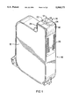
- FIG. 1 is a perspective view of an inkjet print cartridge according to one embodiment of the present invention.
- FIG. 2 is a perspective view of the front surface of the Tape Automated Bonding (TAB) printhead assembly (hereinafter “TAB head assembly”) removed from the print cartridge of FIG. 1.
- TAB head assembly Tape Automated Bonding
- FIG. 3 is a perspective view of an simplified schematic of the inkjet print cartridge of FIG. 1. for illustrative purposes.
- FIG. 4 is a perspective view of the front surface of the Tape Automated Bonding (TAB) printhead assembly (hereinafter “TAB head assembly”) removed from the print cartridge of FIG. 3.
- TAB head assembly Tape Automated Bonding
- FIG. 5 is a perspective view of the back surface of the TAB head assembly of FIG. 4 with a silicon substrate mounted thereon and the conductive leads attached to the substrate.
- FIG. 6 is a side elevational view in cross-section taken along line A--A in FIG. 5 illustrating the attachment of conductive leads to electrodes on the silicon substrate.
- FIG. 7 is a perspective view of the inkjet print cartridge of FIG. 1 with the TAB head assembly removed.
- FIG. 8 is a perspective view of the headland area of the inkjet print cartridge of FIG. 7.
- FIG. 9 is a top plan view of the headland area of the inkjet print cartridge of FIG. 7.
- FIG. 10 is a perspective view of a portion of the inkjet print cartridge of FIG. 3 illustrating the configuration of a seal which is formed between the ink cartridge body and the TAB head assembly.
- FIG. 11 is a top perspective view of a substrate structure containing heater resistors, ink channels, and vaporization chambers, which is mounted on the back of the TAB head assembly of FIG. 4.
- FIG. 12 is a top perspective view, partially cut away, of a portion of the TAB head assembly showing the relationship of an orifice with respect to a vaporization chamber, a heater resistor, and an edge of the substrate.
- FIG. 13 is a schematic cross-sectional view taken along line B--B of FIG. 10 showing the adhesive seal between the TAB head assembly and the print cartridge as well as the ink flow path around the edges of the substrate.
- FIG. 14 is a view of one arrangement of orifices and the associated heater resistors on a printhead.
- FIG. 15 is a schematic diagram of one heater resistor and its associated address line, drive transistor, primitive select line and ground line.
- FIG. 16 is a schematic diagram of the firing sequence for the address select lines when the printer carriage is moving from left to right.
- FIG. 17 is a diagram showing the layout of the contact pads on the TAB head assemble.
- FIG. 18 is a magnified perspective view showing a THA mounted on a print cartridge.
- FIG. 19 shows one end of a substrate with firing resistors #1 and #2, with the interconnects identified.
- FIG. 20 shows the opposite end of the substrate of FIG. 19, with firing resistors #299 and #300, with the interconnects identified.
- FIG. 21 shows the substrate schematics and data taken in a direction along the width of the substrate.
- FIG. 22 shows the substrate schematics and data taken in a direction along the length of the substrate.
- FIG. 23 shows a silicon wafer prior to the individual dies being cut and separated from the wafer.
- FIG. 24 shows the schematic and data for cutting a silicon wafer into individual dies.
- a barrier layer containing ink channels and vaporization chambers is located between a rectangular substrate and a nozzle member containing an array of orifices.
- the substrate contains two linear arrays of heater elements, and each orifice in the nozzle member is associated with a vaporization chamber and heater element.
- the ink channels in the barrier layer have ink entrances generally running along two opposite edges of the substrate so that ink flowing around the edges of the substrate gain access to the ink channels and to the vaporization chambers. Piezoelectric elements can be used instead of heater elements.
- the features of the invention include an ink delivery system for an array of nozzle orifices in a print cartridge comprising an ink reservoir; a substrate having a plurality of individual ink firing chambers with an ink firing element in each chamber; an ink channel connecting said reservoir with said ink firing chambers, said channel including a primary channel connected at a first end with said reservoir and at a second end to a secondary channel; a separate inlet passage for each firing chamber connecting said secondary channel with said firing chamber for allowing high frequency refill of the firing chamber; a group of said firing chambers in adjacent relationship forming a primitive in which only one firing chamber in said primitive is activated at a time; first circuit means on said substrate connected to said firing elements; and second circuit means on said cartridge connected to said first circuit means, for transmitting firing signals to said ink firing elements at a frequency greater than 9 kHz.
- reference numeral 10 generally indicates an inkjet print cartridge incorporating a printhead according to one embodiment of the present invention simplified for illustrative purposes.
- the inkjet print cartridge 10 includes an ink reservoir 12 and a printhead 14, where the printhead 14 is formed using Tape Automated Bonding (TAB).
- TAB head assembly 14 includes a nozzle member 16 comprising two parallel columns of offset holes or orifices 17 formed in a flexible polymer flexible circuit 18 by, for example, laser ablation.
- a back surface of the flexible circuit 18 includes conductive traces 36 formed thereon using a conventional photolithographic etching and/or plating process. These conductive traces 36 are terminated by large contact pads 20 designed to interconnect with a printer.
- the print cartridge 10 is designed to be installed in a printer so that the contact pads 20, on the front surface of the flexible circuit 18, contact printer electrodes providing externally generated energization signals to the printhead.
- Windows 22 and 24 extend through the flexible circuit 18 and are used to facilitate bonding of the other ends of the conductive traces 36 to electrodes on a silicon substrate containing heater resistors.
- the windows 22 and 24 are filled with an encapsulant to protect any underlying portion of the traces and substrate.
- the flexible circuit 18 is bent over the back edge of the print cartridge "snout" and extends approximately one half the length of the back wall 25 of the snout. This flap portion of the flexible circuit 18 is needed for the routing of conductive traces 36 which are connected to the substrate electrodes through the far end window 22.
- the contact pads 20 are located on the flexible circuit 18 which is secured to this wall and the conductive traces 36 are routed over the bend and are connected to the substrate electrodes through the windows 22, 24 in the flexible circuit 18.
- FIG. 2 shows a front view of the TAB head assembly 14 of FIG. 1 removed from the print cartridge 10 and prior to windows 22 and 24 in the TAB head assembly 14 being filled with an encapsulant.
- TAB head assembly 14 has affixed to the back of the flexible circuit 18 a silicon substrate 28 (not shown) containing a plurality of individually energizable thin film resistors. Each resistor is located generally behind a single orifice 17 and acts as an ohmic heater when selectively energized by one or more pulses applied sequentially or simultaneously to one or more of the contact pads 20.
- the orifices 17 and conductive traces 36 may be of any size, number, and pattern, and the various figures are designed to simply and clearly show the features of the invention. The relative dimensions of the various features have been greatly adjusted for the sake of clarity.
- the orifice 17 pattern on the flexible circuit 18 shown in FIG. 2 may be formed by a masking process in combination with a laser or other etching means in a step-and-repeat process, which would be readily understood by one of ordinary skilled in the art after reading this disclosure.
- FIG. 14, to be described in detail later, provides additional details of this process. Further details regarding TAB head assembly 14 and flexible circuit 18 are provided below.
- FIG. 3 is a perspective view of a simplified schematic of the inkjet print cartridge of FIG. 1 for illustrative purposes.
- FIG. 4 is a perspective view of the front surface of the Tape Automated Bonding (TAB) printhead assembly (hereinafter “TAB head assembly”) removed from the simplified schematic print cartridge of FIG. 3.
- TAB Tape Automated Bonding
- FIG. 5 shows the back surface of the TAB head assembly 14 of FIG. 4 showing the silicon die or substrate 28 mounted to the back of the flexible circuit 18 and also showing one edge of the barrier layer 30 formed on the substrate 28 containing ink channels and vaporization chambers.
- FIG. 7 shows greater detail of this barrier layer 30 and will be discussed later. Shown along the edge of the barrier layer 30 are the entrances to the ink channels 32 which receive ink from the ink reservoir 12.
- the conductive traces 36 formed on the back of the flexible circuit 18 terminate in contact pads 20 (shown in FIG. 4) on the opposite side of the flexible circuit 18.
- the windows 22 and 24 allow access to the ends of the conductive traces 36 and the substrate electrodes 40 (shown in FIG. 6) from the other side of the flexible circuit 18 to facilitate bonding.
- FIG. 6 shows a side view cross-section taken along line A--A in FIG. 5 illustrating the connection of the ends of the conductive traces 36 to the electrodes 40 formed on the substrate 28.
- a portion 42 of the barrier layer 30 is used to insulate the ends of the conductive traces 36 from the substrate 28.
- FIG. 7 shows the print cartridge 10 of FIG. 1 with the TAB head assembly 14 removed to reveal the headland pattern 50 used in providing a seal between the TAB head assembly 14 and the printhead body.
- FIG. 8 shows the headland area in enlarged perspective view.
- FIG. 9 shows the headland area in an enlarged top plan view. The headland characteristics are exaggerated for clarity. Shown in FIGS. 8 and 9 is a central slot 52 in the print cartridge 10 for allowing ink from the ink reservoir 12 to flow to the back surface of the TAB head assembly 14.
- the headland pattern 50 formed on the print cartridge 10 is configured so that a bead of epoxy adhesive (not shown) dispensed on the inner raised walls 54 and across the wall openings 55 and 56 (so as to circumscribe the substrate when the TAB head assembly 14 is in place) will form an ink seal between the body of the print cartridge 10 and the back of the TAB head assembly 14 when the TAB head assembly 14 is pressed into place against the headland pattern 50.
- Other adhesives which may be used include hot-melt, silicone, UV curable adhesive, and mixtures thereof.
- a patterned adhesive film may be positioned on the headland, as opposed to dispensing a bead of adhesive.
- the TAB head assembly 14 of FIG. 5 When the TAB head assembly 14 of FIG. 5 is properly positioned and pressed down on the headland pattern 50 in FIG. 8 after the adhesive (not shown) is dispensed, the two short ends of the substrate 28 will be supported by the surface portions 57 and 58 within the wall openings 55 and 56. Additional details regarding adhesive 90 are shown in FIG. 13.
- the configuration of the headland pattern 50 is such that, when the substrate 28 is supported by the surface portions 57 and 58, the back surface of the flexible circuit 18 will be slightly above the top of the raised walls 54 and approximately flush with the flat top surface 59 of the print cartridge 10. As the TAB head assembly 14 is pressed down onto the headland 50, the adhesive is squished down.
- the adhesive From the top of the inner raised walls 54, the adhesive overspills into the gutter between the inner raised walls 54 and the outer raised wall 60 and overspills somewhat toward the slot 52. From the wall openings 55 and 56, the adhesive squishes inwardly in the direction of slot 52 and squishes outwardly toward the outer raised wall 60, which blocks further outward displacement of the adhesive.
- the outward displacement of the adhesive not only serves as an ink seal, but encapsulates the conductive traces in the vicinity of the headland 50 from underneath to protect the traces from ink.
- FIG. 10 shows a portion of the completed print cartridge 10 of FIG. 3 illustrating, by cross-hatching, the location of the underlying adhesive 90 (not shown) which forms the seal between the TAB head assembly 14 and the body of the print cartridge 10.
- the adhesive is located generally between the dashed lines surrounding the array of orifices 17, where the outer dashed line 62 is slightly within the boundaries of the outer raised wall 60 in FIG. 7, and the inner dashed line 64 is slightly within the boundaries of the inner raised walls 54 in FIG. 7.
- the adhesive is also shown being squished through the wall openings 55 and 56 (FIG. 7) to encapsulate the traces leading to electrodes on the substrate. A cross-section of this seal taken along line B--B in FIG. 10 is also shown in FIG. 13, to be discussed later.
- This seal formed by the adhesive 90 circumscribing the substrate 28 allows ink to flow from slot 52 and around the sides of the substrate to the vaporization chambers formed in the barrier layer 30, but will prevent ink from seeping out from under the TAB head assembly 14.
- this adhesive seal 90 provides a strong mechanical coupling of the TAB head assembly 14 to the print cartridge 10, provides a fluidic seal, and provides trace encapsulation.
- the adhesive seal is also easier to cure than prior art seals, and it is much easier to detect leaks between the print cartridge body and the printhead, since the sealant line is readily observable. Further details on adhesive seal 90 are shown in FIG. 13.
- FIG. 11 is a front perspective view of the silicon substrate 28 which is affixed to the back of the flexible circuit 18 in FIG. 5 to form the TAB head assembly 14. Silicon substrate 28 has formed on it, using conventional photolithographic techniques, two rows or columns of thin film resistors 70, shown in FIG. 11 exposed through the vaporization chambers 72 formed in the barrier layer 30.
- the substrate 28 is approximately one-half inch long and contains 300 heater resistors 70, thus enabling a resolution of 600 dots per inch.
- Heater resistors 70 may instead be any other type of ink ejection element, such as a piezoelectric pump-type element or any other conventional element.
- element 70 in all the various figures may be considered to be piezoelectric elements in an alternative embodiment without affecting the operation of the printhead.
- electrodes 74 are also formed on the substrate 28 for connection to the conductive traces 36 (shown by dashed fines) formed on the back of the flexible circuit 18.
- a demultiplexer 78 shown by a dashed outline in FIG. 11, is also formed on the substrate 28 for demultiplexing the incoming multiplexed signals applied to the electrodes 74 and distributing the signals to the various thin film resistors 70.
- the demultiplexer 78 enables the use of much fewer electrodes 74 than thin film resistors 70. Having fewer electrodes allows all connections to the substrate to be made from the short end portions of the substrate, as shown in FIG. 4, so that these connections will not interfere with the ink flow around the long sides of the substrate.
- the demultiplexer 78 may be any decoder for decoding encoded signals applied to the electrodes 74.
- the demultiplexer has input leads (not shown for simplicity) connected to the electrodes 74 and has output leads (not shown) connected to the various resistors 70.
- the demultiplexer 78 circuity is discussed in further detail below.
- barrier layer 30 which may be a layer of photoresist or some other polymer, in which is formed the vaporization chambers 72 and ink channels 80.
- a portion 42 of the barrier layer 30 insulates the conductive traces 36 from the underlying substrate 28, as previously discussed with respect to FIG. 4.
- a thin adhesive layer 84 (not shown), such as an uncured layer of poly-isoprene photoresist, is applied to the top surface of the barrier layer 30.
- a separate adhesive layer may not be necessary if the top of the barrier layer 30 can be otherwise made adhesive.
- the resulting substrate structure is then positioned with respect to the back surface of the flexible circuit 18 so as to align the resistors 70 with the orifices formed in the flexible circuit 18.
- This alignment step also inherently aligns the electrodes 74 with the ends of the conductive traces 36.
- the traces 36 are then bonded to the electrodes 74. This alignment and bonding process is described in more detail later with respect to FIG. 14.
- the aligned and bonded substrate/flexible circuit structure is then heated while applying pressure to cure the adhesive layer 84 and firmly affix the substrate structure to the back surface of the flexible circuit 18.
- FIG. 12 is an enlarged view of a single vaporization chamber 72, thin film resistor 70, and frustum shaped orifice 17 after the substrate structure of FIG. 11 is secured to the back of the flexible circuit 18 via the thin adhesive layer 84.
- a side edge of the substrate 28 is shown as edge 86.
- ink flows from the ink reservoir 12 around the side edge 86 of the substrate 28, and into the ink channel 80 and associated vaporization chamber 72, as shown by the arrow 88.
- Upon energization of the thin film resistor 70 a thin layer of the adjacent ink is superheated, causing explosive vaporization and, consequently, causing a droplet of ink to be ejected through the orifice 17.
- the vaporization chamber 72 is then refilled by capillary action.
- the barrier layer 30 is approximately 1 mils thick, the substrate 28 is approximately 20 mils thick, and the flexible circuit 18 is approximately 2 mils thick.
- FIG. 13 Shown in FIG. 13 is a side elevational view cross-section taken along line B--B in FIG. 10 showing a portion of the adhesive seal 90, applied to the inner raised wall 54 and wall openings 55, 56, surrounding the substrate 28 and showing the substrate 28 being adhesively secured to a central portion of the flexible circuit 18 by the thin adhesive layer 84 on the top surface of the barrier layer 30 containing the ink channels and vaporization chambers 92 and 94.
- FIG. 13 also illustrates how ink 88 from the ink reservoir 12 flows through the central slot 52 formed in the print cartridge 10 and flows around the edges 86 of the substrate 28 through ink channels 80 into the vaporization chambers 92 and 94.
- Thin film resistors 96 and 98 are shown within the vaporization chambers 92 and 94, respectively. When the resistors 96 and 98 are energized, the ink within the vaporization chambers 92 and 94 are ejected, as illustrated by the emitted drops of ink 101 and 102.
- the edge feed feature where ink flows around the edges 86 of the substrate 28 and directly into ink channels 80, has a number of advantages over previous center feed printhead designs which form an elongated central hole or slot running lengthwise in the substrate to allow ink to flow into a central manifold and ultimately to the entrances of ink channels.
- One advantage is that the substrate or die 28 width can be made narrower, due to the absence of the elongated central hole or slot in the substrate. Not only can the substrate be made narrower, but the length of the edge feed substrate can be shorter, for the same number of nozzles, than the center feed substrate due to the substrate structure now being less prone to cracking or breaking without the central ink feed hole.
- This shortening of the substrate 28 enables a shorter headland 50 in FIG. 8 and, hence, a shorter print cartridge snout.
- the star wheels can be located closer to the pinch rollers to ensure better paper/roller contact along the transport path of the print cartridge snout. Additionally, by making the substrate smaller, more substrates can be formed per wafer, thus lowering the material cost per substrate.
- edge feed feature manufacturing time is saved by not having to etch a slot in the substrate, and the substrate is less prone to breakage during handling. Further, the substrate is able to dissipate more heat, since the ink flowing across the back of the substrate and around the edges of the substrate acts to draw heat away from the back of the substrate.
- the edge feed design Be eliminating the manifold as well as the slot in the substrate, the ink is able to flow more rapidly into the vaporization chambers, since there is less restriction on the ink flow. This more rapid ink flow improves the frequency response of the printhead, allowing higher printing rates from a given number of orifices. Further, the more rapid ink flow reduces crosstalk between nearby vaporization chambers caused by variations in ink flow as the heater elements in the vaporization chambers are fired.
- the ink reservoir contains two separate ink sources, each containing a different color of ink.
- the central slot 52 in FIG. 13 is bisected, as shown by the dashed line 103, so that each side of the central slot 52 communicates with a separate ink source. Therefore, the left linear array of vaporization chambers can be made to eject one color of ink, while the right linear array of vaporization chambers can be made to eject a different color of ink.
- This concept can even be used to create a four color printhead, where a different ink reservoir feeds ink to ink channels along each of the four sides of the substrate.
- a four-edge design would be used, preferably using a square substrate for symmetry.
- the TAB head assembly is positioned on the print cartridge 10, and the previously described adhesive seal 90 is formed to firmly secure the nozzle member to the print cartridge, provide an ink-proof seal around the substrate between the nozzle member and the ink reservoir, and encapsulate the traces in the vicinity of the headland so as to isolate the traces from the ink.
- Peripheral points on the flexible TAB head assembly are then secured to the plastic print cartridge 10 by a conventional melt-through type bonding process to cause the polymer flexible circuit 18 to remain relatively flush with the surface of the print cartridge 10, as shown in FIG. 1.
- the printhead nozzles must be placed closer together. This requires that both heater resistors and the associated orifices be placed closer together.
- the orifices 17 in the nozzle member 16 of the TAB head assembly are generally arranged in two major columns of orifices 17 as shown in FIG. 14.
- the orifices 17 are conventionally assigned a number as shown, starting at the top right as the TAB head assembly as viewed from the external surface of the nozzle member 16 and ending in the lower left, thereby resulting in the odd numbers being arranged in one column and even numbers being arranged in the second column.
- the orifices/resistors in each column are spaced 1/300 of an inch apart in the long direction of the nozzle member.
- the orifices and resistors in one column are offset from the orifice/resistors in the other column in the long direction of the nozzle member by 1/600 of an inch, thus, providing 600 dots per inch (dpi) printing.
- the orifices 17, while aligned in two major columns as described, are further arranged in an offset pattern within each column to match the offset heater resistors 70 disposed in the substrate 28 as illustrated in FIG. 14.
- a small offset E is provided between resistors. This small offset E allows adjacent resistors 70 to be fired at slightly different times when the TAB head assembly is scanning across the recording medium to further minimize cross-talk effects between adjacent vaporization chambers 130.
- the resistors are fired at twenty two different times, the offset allows the ejected ink drops from different nozzles to be placed in the same horizontal position on the print media.
- the resistors 70 are coupled to electrical drive circuitry (not shown in FIG.
- the firing heater resistors 70 of the preferred embodiment are organized as fourteen primitive groups of twenty or twenty-two resistors. It can be seen that each resistor (numbered 1 through 300 and corresponding to the orifices 17 of FIG. 14) is controlled by its own FET drive transistor, which shares its control input Address Select (A1-A22) with thirteen other resistors. Each resistor is tied to nineteen or twenty-one other resistors by a common node Primitive Select (PS1-PS14). Consequently, firing a particular resistor requires applying a control voltage at its "Address Select" terminal and an electrical power source at its "Primitive Select" terminal. Only one Address Select line is enabled at one time.
- FIG. 15 is a schematic diagram of an individual heater resistor and its FET drive transistor. As shown in FIG. 15, Address Select and Primitive Select lines also contain transistors for draining unwanted electrostatic discharge and pull down resistors to place all unselected addresses in an off state. Table I shows the correlation between the firing resistor/orifice and the Address Select and Primitive Select Lines.
- the Address Select lines are sequentially turned on via TAB head assembly interface circuitry according to a firing order counter located in the printer and sequenced (independently of the data directing which resistor is to be energized) from A1 to A22 when printing form left to right and from A22 to A1 when printing from right to left.
- the print data retrieved from the printer memory turns on any combination of the Primitive Select lines.
- Primitive Select lines (instead of Address Select lines) are used in the preferred embodiment to control the pulse width. Disabling Address Select lines while the drive transistors are conducting high current can cause avalanche breakdown and consequent physical damage to MOS transistors. Accordingly, the Address Select lines are "set" before power is applied to the Primitive Select lines, and conversely, power is turned off before the Address Select lines are changed.
- each primitive is selectively fired by powering the associated primitive select interconnection.
- To provide uniform energy per heater resistor only one resistor is energized at a time per primitive.
- any number of the primitive selects may be enabled concurrently.
- Each enabled primitive select thus delivers both power and one of the enable signals to the driver transistor.
- the other enable signal is an address signal provided by each address select line only one of which is active at a time.
- Each address select line is tied to all of the switching transistors so that all such switching devices are conductive when the interconnection is enabled. Where a primitive select interconnection and an address select line for a heater resistor are both active simultaneously, that particular heater resistor is energized.
- FIG. 16 shows the firing sequence when the print carriage is scanning from left to right. The firing sequence is reversed when scanning from right to left.
- the resistor firing frequency is shown as F in FIG. 16. A brief rest period of approximately ten percent of the period, 1/F is allowed between cycles. This rest period prevents Address Select cycles from overlapping due to printer carriage velocity variations.
- the interconnections for controlling the TAB head assembly driver circuitry include separate primitive select and primitive common interconnections.
- the driver circuity of the preferred embodiment comprises an array of fourteen primitives, fourteen primitive commons, and twenty-two address select lines, thus requiring 50 interconnections to control 300 firing resistors.
- the integration of both heater resistors and FET driver transistors onto a common substrate creates the need for additional layers of conductive circuitry on the substrate so that the transistors could be electrically connected to the resistors and other components of the system. This creates a concentration of heat generation within the substrate.
- the print cartridge 10 is designed to be installed in a printer so that the contact pads 20, on the front surface of the flexible circuit 18, contact printer electrodes which couple externally generated energization signals to the TAB head assembly.
- To access the traces 36 on the back surface of the flexible circuit 18 from the front surface of the flexible circuit holes (vias) are formed through the front surface of the flexible circuit to expose the ends of the traces.
- the exposed ends of the traces are then plated with, for example, gold to form the contact pads 20 shown on the front surface of the flexible circuit in FIG. 2.
- the contact or interface pads 20 are assigned the functions listed in Table II.
- FIG. 17 shows the location of the interface pads 20 on the TAB head assembly of FIG. 2.
- FIG. 18 shows the relative positions of the even # nozzles 2 through 300 and the odd # nozzles 1 through 299 when the THA is mounted on a print cartridge.
- FIGS. 19-20 are an enlarged illustration of both truncated end portions 202, 204 of the substrate showing the ESD devices 206 and the interconnect junctions 208.
- FIGS. 21-22 includes schematic drawings as well as related data tables showing the dimensions, electrical resistance and identification of the various circuitry portions of the substrate. It will be appreciated by those skilled in the art that substantial heat is generated by all of the circuitry on the substrate. More particularly, each firing resistor requires 300 milliamps whenever it is selected for firing. For a 12 KHertz firing frequency of F, and in reference to the firing diagram of FIG. 16, when all of the twenty-two address lines are activated in a duty cycle with each pulse width being 2.3 microseconds, then 2.3 ⁇ 22 equals a result divided by 83 microseconds to create a 61% duty cycle. Therefore it is possible when all primitives are firing at the same time to pass a current of approximately 25 amps through the substrate (300 milliamps ⁇ 14 ⁇ 0.61). The cooling characteristices of the edge feed design are therefore very helpful in avoiding the overheating of the substrate during normal operation.
- FIGS. 23-24 show the dimensions for cutting a silicon wafer in order to obtain a high yield for the substrate dies of the present invention.
- some of the dies such as 210 which extend into the 5 mm wide exclusion zone 212 are not usable if critical components of the multilayer substrate lie inside such exclusion zone, nevertheless the invention still provides significantly better yield than for an estimated yield for a center feed ink channel design having the same 300 nozzle 600 dpi specifications as the presently preferred embodiment of the present invention.
Abstract
Description
TABLE I
__________________________________________________________________________
Nozzle Number by Address Select and Primitive Select Lines
P1 P2
P3
P4
P5 P6 P7 P8 P9 P10
P11
P12
P13
P14
__________________________________________________________________________
A1
1 45
42
89
86
133
130
177
174
221
218
265
262
A2
7
4
51
48
95
92
139
136
183
180
227
224
271
268
A3
13
10
57
54
101
98
145
142
189
186
233
230
277
274
A4
19
16
63
60
107
104
151
148
195
192
239
236
283
280
A5
25
22
69
66
113
110
157
154
201
198
245
242
289
286
A6
31
28
75
72
119
116
163
160
207
204
251
248
295
292
A7
37
34
81
78
125
122
169
166
213
210
257
254 298
A8 40
43
84
87
128
131
172
175
216
219
260
263
A9
5
2
49
46
93
90
137
134
181
178
225
222
269
266
A10
11
8
55
52
99
96
143
140
187
184
231
228
275
272
A11
17
14
61
58
105
102
149
146
193
190
237
234
281
278
A12
23
20
67
64
111
108
155
152
199
196
243
240
287
284
A13
29
26
73
70
117
114
161
158
205
202
249
246
293
290
A14
35
32
79
76
123
120
167
164
211
208
255
252
299
296
A15 38
41
82
85
126
129
170
173
214
217
258
261
A16
3 47
44
91
88
135
132
179
176
223
220
267
264
A17
9
6
53
50
97
94
141
138
185
182
229
226
273
270
A18
15
12
59
56
103
100
147
144
191
188
235
232
279
276
A19
21
18
65
62
109
106
153
150
197
194
241
238
285
282
A20
27
24
71
68
115
112
159
156
203
200
247
244
291
288
A21
33
30
77
74
121
118
165
162
209
206
253
250
297
294
A22
39
36
83
80
127
124
171
168
215
212
259
256 300
__________________________________________________________________________
              TABLE II
______________________________________
ELECTRICAL PAD DEFINITION
Odd Side of Head  Even Side of Head
Pad # Name    Function    Pad # Name  Function
______________________________________
 1    A9      Address Select
                           2    G6    Common 6
              9
 3    PS7     Primitive    4    PS6   Primitive
              Select 7                Select 6
 5    G7      Common 7     6    A11   Address
                                      Select 11
 7    PS5     Primitive Select
                           8    A13   Address
              5                       Select 13
 9    G5      Common 5    10    G4    Common 4
11    G3      Common 3    12    PS4   Primitive
                                      Select 4
13    PS3     Primitive Select
                          14    A15   Address
              3                       Select 15
15    A7      Address Select
                          16    A17   Address
              7                       Select 17
17    A5      Address Select
                          18    G2    Common 2
              5
19    G1      Common 1    20    PS2   Primitive
                                      Select 2
21    PS1     Primitive Select
                          22    A19   Address
              1                       Select 19
23    A3      Address Select
                          24    A21   Address
              3                       Select 21
25    A1      Address Select
                          26    A22   Address
              1                       Select 22
27    TSR     Thermal Sense
                          28    R10X  10X Resistor
29    A2      Address Select
                          30    A20   Address
              2                       Select 20
31    A4      Address Select
                          32    PS14  Primitive
              4                       Select 14
33    PS13    Primitive Select
                          34    G14   Common 14
              13
35    G13     Common 13   36    A18   Address
                                      Select 18
37    A6      Address Select
                          38    A 16  Address
              6                       Select 16
39    A8      Address Select
                          40    PS12  Primitive
              8                       Select 12
41    PS11    Primitive Select
                          42    G12   Common 12
              11
43    G11     Common 11   44    G10   Common 10
45    A10     Address Select
                          46    PS10  Primitive
              10                      Select 10
47    A12     Address Select
                          48    G8    Common 8
              12
49    PS9     Primitive Select
                          50    PS8   Primitive
              9                       Select 8
51    G9      Common 9    52    A14   Address
                                      Select 14
______________________________________
Claims (39)
Priority Applications (1)
| Application Number | Priority Date | Filing Date | Title |
|---|---|---|---|
| US08/319,895 US5568171A (en) | 1992-04-02 | 1994-10-06 | Compact inkjet substrate with a minimal number of circuit interconnects located at the end thereof |
Applications Claiming Priority (3)
| Application Number | Priority Date | Filing Date | Title |
|---|---|---|---|
| US07/862,086 US5278584A (en) | 1992-04-02 | 1992-04-02 | Ink delivery system for an inkjet printhead |
| US08/179,866 US5625396A (en) | 1992-04-02 | 1994-01-11 | Ink delivery method for an inkjet print cartridge |
| US08/319,895 US5568171A (en) | 1992-04-02 | 1994-10-06 | Compact inkjet substrate with a minimal number of circuit interconnects located at the end thereof |
Related Parent Applications (1)
| Application Number | Title | Priority Date | Filing Date |
|---|---|---|---|
| US08/179,866 Continuation-In-Part US5625396A (en) | 1992-04-02 | 1994-01-11 | Ink delivery method for an inkjet print cartridge |
Publications (1)
| Publication Number | Publication Date |
|---|---|
| US5568171A true US5568171A (en) | 1996-10-22 |
Family
ID=46202500
Family Applications (1)
| Application Number | Title | Priority Date | Filing Date |
|---|---|---|---|
| US08/319,895 Expired - Lifetime US5568171A (en) | 1992-04-02 | 1994-10-06 | Compact inkjet substrate with a minimal number of circuit interconnects located at the end thereof |
Country Status (1)
| Country | Link |
|---|---|
| US (1) | US5568171A (en) |
Cited By (24)
| Publication number | Priority date | Publication date | Assignee | Title |
|---|---|---|---|---|
| US5689296A (en) * | 1995-11-02 | 1997-11-18 | Pitney Bowes Inc. | Digital printing apparatus |
| WO1998055316A1 (en) * | 1997-06-06 | 1998-12-10 | Minnesota Mining And Manufacturing Company | Bonding system in an inkjet printer pen and method for providing the same |
| US5883650A (en) * | 1995-12-06 | 1999-03-16 | Hewlett-Packard Company | Thin-film printhead device for an ink-jet printer |
| US6132032A (en) * | 1999-08-13 | 2000-10-17 | Hewlett-Packard Company | Thin-film print head for thermal ink-jet printers |
| US6239820B1 (en) | 1995-12-06 | 2001-05-29 | Hewlett-Packard Company | Thin-film printhead device for an ink-jet printer |
| EP1080898A3 (en) * | 1999-08-30 | 2001-08-16 | Hewlett-Packard Company, A Delaware Corporation | Redundant input signal paths for an inkjet print head |
| US6314660B1 (en) | 1998-11-04 | 2001-11-13 | Hewlett-Packard Company | Cascaded tensioning tangential drive for THA handling |
| EP1093920A3 (en) * | 1999-10-18 | 2002-02-20 | Hewlett-Packard Company, A Delaware Corporation | Large thermal ink jet nozzle array printhead |
| US6378984B1 (en) | 1998-07-31 | 2002-04-30 | Hewlett-Packard Company | Reinforcing features in flex circuit to provide improved performance in a thermal inkjet printhead |
| US6398346B1 (en) | 2000-03-29 | 2002-06-04 | Lexmark International, Inc. | Dual-configurable print head addressing |
| US6431677B1 (en) | 2000-06-08 | 2002-08-13 | Lexmark International, Inc | Print head drive scheme |
| US20030035407A1 (en) * | 2000-03-27 | 2003-02-20 | Rangaprasad Govindarajan | Packet retransmission in wireless packet data networks |
| US6543883B1 (en) | 2001-09-29 | 2003-04-08 | Hewlett-Packard Company | Fluid ejection device with drive circuitry proximate to heating element |
| US6619786B2 (en) | 2001-06-08 | 2003-09-16 | Lexmark International, Inc. | Tab circuit for ink jet printer cartridges |
| US6685291B1 (en) * | 1999-11-29 | 2004-02-03 | Canon Kabushiki Kaisha | Printing apparatus and printing method |
| US20040087063A1 (en) * | 2002-10-31 | 2004-05-06 | Mohammad Akhavin | Edge-sealed substrates and methods for effecting the same |
| US20060221140A1 (en) * | 2005-04-01 | 2006-10-05 | Lexmark International, Inc. | Low profile printhead |
| US20060226139A1 (en) * | 2005-04-06 | 2006-10-12 | Craig Jennings | Wok-piece positioner |
| WO2009018316A1 (en) * | 2007-07-31 | 2009-02-05 | Hewlett-Packard Development Company, L.P. | Printheads |
| US20090205311A1 (en) * | 2006-11-10 | 2009-08-20 | Aerojet-General Corporation, A Corporation Of The State Of Ohio | Combined cycle missile engine system |
| US20100244269A1 (en) * | 2009-03-31 | 2010-09-30 | Samsung Electronics Co., Ltd. | Semiconductor device having integral structure of contact pad and conductive line |
| US20130076834A1 (en) * | 2011-09-22 | 2013-03-28 | Fujifilm Corporation | Inkjet head and method for producing the same |
| US20150305140A1 (en) * | 2014-04-18 | 2015-10-22 | Xerox Corporation | Circuit board reflow of components using on board copper traces as heating element |
| US20180056319A1 (en) * | 2014-06-20 | 2018-03-01 | Stmicroelectronics, Inc. | Microfluidic system with single drive signal for multiple nozzles |
Citations (22)
| Publication number | Priority date | Publication date | Assignee | Title |
|---|---|---|---|---|
| US4312009A (en) * | 1979-02-16 | 1982-01-19 | Smh-Adrex | Device for projecting ink droplets onto a medium |
| US4502060A (en) * | 1983-05-02 | 1985-02-26 | Hewlett-Packard Company | Barriers for thermal ink jet printers |
| US4558333A (en) * | 1981-07-09 | 1985-12-10 | Canon Kabushiki Kaisha | Liquid jet recording head |
| US4587534A (en) * | 1983-01-28 | 1986-05-06 | Canon Kabushiki Kaisha | Liquid injection recording apparatus |
| US4611219A (en) * | 1981-12-29 | 1986-09-09 | Canon Kabushiki Kaisha | Liquid-jetting head |
| US4683481A (en) * | 1985-12-06 | 1987-07-28 | Hewlett-Packard Company | Thermal ink jet common-slotted ink feed printhead |
| US4695854A (en) * | 1986-07-30 | 1987-09-22 | Pitney Bowes Inc. | External manifold for ink jet array |
| US4712172A (en) * | 1984-04-17 | 1987-12-08 | Canon Kabushiki Kaisha | Method for preventing non-discharge in a liquid jet recorder and a liquid jet recorder |
| US4734717A (en) * | 1986-12-22 | 1988-03-29 | Eastman Kodak Company | Insertable, multi-array print/cartridge |
| US4791440A (en) * | 1987-05-01 | 1988-12-13 | International Business Machine Corporation | Thermal drop-on-demand ink jet print head |
| US4847630A (en) * | 1987-12-17 | 1989-07-11 | Hewlett-Packard Company | Integrated thermal ink jet printhead and method of manufacture |
| US4878070A (en) * | 1988-10-17 | 1989-10-31 | Xerox Corporation | Thermal ink jet print cartridge assembly |
| US4922269A (en) * | 1984-06-11 | 1990-05-01 | Canon Kabushiki Kaisha | Liquid jet recording head unit, method of making same and liquid jet recording apparatus incorporating same |
| US4940413A (en) * | 1989-07-26 | 1990-07-10 | Hewlett-Packard Company | Electrical make/break interconnect having high trace density |
| US4942408A (en) * | 1989-04-24 | 1990-07-17 | Eastman Kodak Company | Bubble ink jet print head and cartridge construction and fabrication method |
| US4999650A (en) * | 1989-12-18 | 1991-03-12 | Eastman Kodak Company | Bubble jet print head having improved multiplex actuation construction |
| US5016023A (en) * | 1989-10-06 | 1991-05-14 | Hewlett-Packard Company | Large expandable array thermal ink jet pen and method of manufacturing same |
| US5059989A (en) * | 1990-05-16 | 1991-10-22 | Lexmark International, Inc. | Thermal edge jet drop-on-demand ink jet print head |
| US5091737A (en) * | 1981-10-13 | 1992-02-25 | Canon Kabushiki Kaisha | Recording device |
| US5097274A (en) * | 1990-06-18 | 1992-03-17 | Xerox Corporation | Overlapping chip replaceable subunits, methods of making same, and methods of making RIS or ROS array bars incorporating these subunits |
| US5198834A (en) * | 1991-04-02 | 1993-03-30 | Hewlett-Packard Company | Ink jet print head having two cured photoimaged barrier layers |
| US5315472A (en) * | 1991-07-23 | 1994-05-24 | Hewlett Packard Company | Ground ring/spark gap ESD protection of tab circuits |
-
1994
- 1994-10-06 US US08/319,895 patent/US5568171A/en not_active Expired - Lifetime
Patent Citations (22)
| Publication number | Priority date | Publication date | Assignee | Title |
|---|---|---|---|---|
| US4312009A (en) * | 1979-02-16 | 1982-01-19 | Smh-Adrex | Device for projecting ink droplets onto a medium |
| US4558333A (en) * | 1981-07-09 | 1985-12-10 | Canon Kabushiki Kaisha | Liquid jet recording head |
| US5091737A (en) * | 1981-10-13 | 1992-02-25 | Canon Kabushiki Kaisha | Recording device |
| US4611219A (en) * | 1981-12-29 | 1986-09-09 | Canon Kabushiki Kaisha | Liquid-jetting head |
| US4587534A (en) * | 1983-01-28 | 1986-05-06 | Canon Kabushiki Kaisha | Liquid injection recording apparatus |
| US4502060A (en) * | 1983-05-02 | 1985-02-26 | Hewlett-Packard Company | Barriers for thermal ink jet printers |
| US4712172A (en) * | 1984-04-17 | 1987-12-08 | Canon Kabushiki Kaisha | Method for preventing non-discharge in a liquid jet recorder and a liquid jet recorder |
| US4922269A (en) * | 1984-06-11 | 1990-05-01 | Canon Kabushiki Kaisha | Liquid jet recording head unit, method of making same and liquid jet recording apparatus incorporating same |
| US4683481A (en) * | 1985-12-06 | 1987-07-28 | Hewlett-Packard Company | Thermal ink jet common-slotted ink feed printhead |
| US4695854A (en) * | 1986-07-30 | 1987-09-22 | Pitney Bowes Inc. | External manifold for ink jet array |
| US4734717A (en) * | 1986-12-22 | 1988-03-29 | Eastman Kodak Company | Insertable, multi-array print/cartridge |
| US4791440A (en) * | 1987-05-01 | 1988-12-13 | International Business Machine Corporation | Thermal drop-on-demand ink jet print head |
| US4847630A (en) * | 1987-12-17 | 1989-07-11 | Hewlett-Packard Company | Integrated thermal ink jet printhead and method of manufacture |
| US4878070A (en) * | 1988-10-17 | 1989-10-31 | Xerox Corporation | Thermal ink jet print cartridge assembly |
| US4942408A (en) * | 1989-04-24 | 1990-07-17 | Eastman Kodak Company | Bubble ink jet print head and cartridge construction and fabrication method |
| US4940413A (en) * | 1989-07-26 | 1990-07-10 | Hewlett-Packard Company | Electrical make/break interconnect having high trace density |
| US5016023A (en) * | 1989-10-06 | 1991-05-14 | Hewlett-Packard Company | Large expandable array thermal ink jet pen and method of manufacturing same |
| US4999650A (en) * | 1989-12-18 | 1991-03-12 | Eastman Kodak Company | Bubble jet print head having improved multiplex actuation construction |
| US5059989A (en) * | 1990-05-16 | 1991-10-22 | Lexmark International, Inc. | Thermal edge jet drop-on-demand ink jet print head |
| US5097274A (en) * | 1990-06-18 | 1992-03-17 | Xerox Corporation | Overlapping chip replaceable subunits, methods of making same, and methods of making RIS or ROS array bars incorporating these subunits |
| US5198834A (en) * | 1991-04-02 | 1993-03-30 | Hewlett-Packard Company | Ink jet print head having two cured photoimaged barrier layers |
| US5315472A (en) * | 1991-07-23 | 1994-05-24 | Hewlett Packard Company | Ground ring/spark gap ESD protection of tab circuits |
Cited By (35)
| Publication number | Priority date | Publication date | Assignee | Title |
|---|---|---|---|---|
| US5689296A (en) * | 1995-11-02 | 1997-11-18 | Pitney Bowes Inc. | Digital printing apparatus |
| US5883650A (en) * | 1995-12-06 | 1999-03-16 | Hewlett-Packard Company | Thin-film printhead device for an ink-jet printer |
| US6153114A (en) * | 1995-12-06 | 2000-11-28 | Hewlett-Packard Company | Thin-film printhead device for an ink-jet printer |
| US6239820B1 (en) | 1995-12-06 | 2001-05-29 | Hewlett-Packard Company | Thin-film printhead device for an ink-jet printer |
| WO1998055316A1 (en) * | 1997-06-06 | 1998-12-10 | Minnesota Mining And Manufacturing Company | Bonding system in an inkjet printer pen and method for providing the same |
| US6378984B1 (en) | 1998-07-31 | 2002-04-30 | Hewlett-Packard Company | Reinforcing features in flex circuit to provide improved performance in a thermal inkjet printhead |
| US6314660B1 (en) | 1998-11-04 | 2001-11-13 | Hewlett-Packard Company | Cascaded tensioning tangential drive for THA handling |
| US6132032A (en) * | 1999-08-13 | 2000-10-17 | Hewlett-Packard Company | Thin-film print head for thermal ink-jet printers |
| EP1080898A3 (en) * | 1999-08-30 | 2001-08-16 | Hewlett-Packard Company, A Delaware Corporation | Redundant input signal paths for an inkjet print head |
| US6582062B1 (en) | 1999-10-18 | 2003-06-24 | Hewlett-Packard Development Company, L.P. | Large thermal ink jet nozzle array printhead |
| EP1093920A3 (en) * | 1999-10-18 | 2002-02-20 | Hewlett-Packard Company, A Delaware Corporation | Large thermal ink jet nozzle array printhead |
| US6685291B1 (en) * | 1999-11-29 | 2004-02-03 | Canon Kabushiki Kaisha | Printing apparatus and printing method |
| US20030035407A1 (en) * | 2000-03-27 | 2003-02-20 | Rangaprasad Govindarajan | Packet retransmission in wireless packet data networks |
| US6398346B1 (en) | 2000-03-29 | 2002-06-04 | Lexmark International, Inc. | Dual-configurable print head addressing |
| US6431677B1 (en) | 2000-06-08 | 2002-08-13 | Lexmark International, Inc | Print head drive scheme |
| US6619786B2 (en) | 2001-06-08 | 2003-09-16 | Lexmark International, Inc. | Tab circuit for ink jet printer cartridges |
| US6543883B1 (en) | 2001-09-29 | 2003-04-08 | Hewlett-Packard Company | Fluid ejection device with drive circuitry proximate to heating element |
| US20040087063A1 (en) * | 2002-10-31 | 2004-05-06 | Mohammad Akhavin | Edge-sealed substrates and methods for effecting the same |
| US6951778B2 (en) | 2002-10-31 | 2005-10-04 | Hewlett-Packard Development Company, L.P. | Edge-sealed substrates and methods for effecting the same |
| US20060221140A1 (en) * | 2005-04-01 | 2006-10-05 | Lexmark International, Inc. | Low profile printhead |
| US20060226139A1 (en) * | 2005-04-06 | 2006-10-12 | Craig Jennings | Wok-piece positioner |
| US20090205311A1 (en) * | 2006-11-10 | 2009-08-20 | Aerojet-General Corporation, A Corporation Of The State Of Ohio | Combined cycle missile engine system |
| US8056319B2 (en) | 2006-11-10 | 2011-11-15 | Aerojet—General Corporation | Combined cycle missile engine system |
| US20090033695A1 (en) * | 2007-07-31 | 2009-02-05 | Burton Gregory N | Printheads |
| WO2009018316A1 (en) * | 2007-07-31 | 2009-02-05 | Hewlett-Packard Development Company, L.P. | Printheads |
| CN101765506B (en) * | 2007-07-31 | 2013-06-19 | 惠普开发有限公司 | Printheads |
| US8651604B2 (en) | 2007-07-31 | 2014-02-18 | Hewlett-Packard Development Company, L.P. | Printheads |
| US20100244269A1 (en) * | 2009-03-31 | 2010-09-30 | Samsung Electronics Co., Ltd. | Semiconductor device having integral structure of contact pad and conductive line |
| US8304886B2 (en) * | 2009-03-31 | 2012-11-06 | Samsung Electronics Co., Ltd | Semiconductor device having integral structure of contact pad and conductive line |
| US20130076834A1 (en) * | 2011-09-22 | 2013-03-28 | Fujifilm Corporation | Inkjet head and method for producing the same |
| US20150305140A1 (en) * | 2014-04-18 | 2015-10-22 | Xerox Corporation | Circuit board reflow of components using on board copper traces as heating element |
| US10009993B2 (en) * | 2014-04-18 | 2018-06-26 | Xerox Corporation | Circuit board reflow of components using on board copper traces as heating element |
| US20180056319A1 (en) * | 2014-06-20 | 2018-03-01 | Stmicroelectronics, Inc. | Microfluidic system with single drive signal for multiple nozzles |
| US10543504B2 (en) | 2014-06-20 | 2020-01-28 | Stmicroelectronics, Inc. | Microfluidic system with single drive signal for multiple nozzles |
| US10646892B2 (en) * | 2014-06-20 | 2020-05-12 | Stmicroelectronics, Inc. | Microfluidic system with single drive signal for multiple nozzles |
Similar Documents
| Publication | Publication Date | Title |
|---|---|---|
| US5648804A (en) | Compact inkjet substrate with centrally located circuitry and edge feed ink channels | |
| US5648806A (en) | Stable substrate structure for a wide swath nozzle array in a high resolution inkjet printer | |
| US5568171A (en) | Compact inkjet substrate with a minimal number of circuit interconnects located at the end thereof | |
| US5648805A (en) | Inkjet printhead architecture for high speed and high resolution printing | |
| US5604519A (en) | Inkjet printhead architecture for high frequency operation | |
| US5638101A (en) | High density nozzle array for inkjet printhead | |
| US5563642A (en) | Inkjet printhead architecture for high speed ink firing chamber refill | |
| US5594481A (en) | Ink channel structure for inkjet printhead | |
| US6474789B1 (en) | Recording apparatus, recording head and substrate therefor | |
| JP3404470B2 (en) | Inkjet print head | |
| KR101112533B1 (en) | Fluid Ejection Device | |
| US8651604B2 (en) | Printheads | |
| US20050030358A1 (en) | Filter for printhead assembly | |
| JPH0994968A (en) | Ink jet print head | |
| US7798611B2 (en) | Circuit routing for printhead having increased corrosion resistance | |
| JP2003175609A (en) | Method and structure for sealing wire-bonded portion of semiconductor chip, and printer head | |
| JPH02141246A (en) | Ink-jet recording head |
Legal Events
| Date | Code | Title | Description |
|---|---|---|---|
| AS | Assignment |
Owner name: HEWLETT-PACKARD COMPANY, CALIFORNIA Free format text: ASSIGNMENT OF ASSIGNORS INTEREST;ASSIGNORS:KEEFE, BRIAN J.;CHILDERS, WINTHROP D.;STEINFIELD, STEVEN W.;AND OTHERS;REEL/FRAME:007643/0694;SIGNING DATES FROM 19941218 TO 19950331 |
|
| STCF | Information on status: patent grant |
Free format text: PATENTED CASE |
|
| FPAY | Fee payment |
Year of fee payment: 4 |
|
| AS | Assignment |
Owner name: HEWLETT-PACKARD COMPANY, COLORADO Free format text: MERGER;ASSIGNOR:HEWLETT-PACKARD COMPANY;REEL/FRAME:011523/0469 Effective date: 19980520 |
|
| FEPP | Fee payment procedure |
Free format text: PAYOR NUMBER ASSIGNED (ORIGINAL EVENT CODE: ASPN); ENTITY STATUS OF PATENT OWNER: LARGE ENTITY |
|
| FPAY | Fee payment |
Year of fee payment: 8 |
|
| FPAY | Fee payment |
Year of fee payment: 12 |
|
| REMI | Maintenance fee reminder mailed | ||
| AS | Assignment |
Owner name: HEWLETT-PACKARD DEVELOPMENT COMPANY, L.P., TEXAS Free format text: ASSIGNMENT OF ASSIGNORS INTEREST;ASSIGNOR:HEWLETT-PACKARD COMPANY;REEL/FRAME:026945/0699 Effective date: 20030131 |