US5729683A - Programming memory devices through the parallel port of a computer system - Google Patents
Programming memory devices through the parallel port of a computer system Download PDFInfo
- Publication number
- US5729683A US5729683A US08/444,068 US44406895A US5729683A US 5729683 A US5729683 A US 5729683A US 44406895 A US44406895 A US 44406895A US 5729683 A US5729683 A US 5729683A
- Authority
- US
- United States
- Prior art keywords
- signal
- signals
- parallel port
- state
- command
- Prior art date
- Legal status (The legal status is an assumption and is not a legal conclusion. Google has not performed a legal analysis and makes no representation as to the accuracy of the status listed.)
- Expired - Lifetime
Links
Images


Classifications
-
- G—PHYSICS
- G06—COMPUTING; CALCULATING OR COUNTING
- G06F—ELECTRIC DIGITAL DATA PROCESSING
- G06F8/00—Arrangements for software engineering
- G06F8/60—Software deployment
Definitions
- the invention relates to the transfer of data through the parallel port of a computer system, and more particularly, to a technique of programming memory in the computer system through the parallel port.
- Modern computers are typically managed by a supervisory program called an operating system.
- an operating system In a computer system, several concurrent processes are usually competing for system resources, which include memory and I/O address space, DMA channels and interrupt levels.
- a basic function of the operating system is to schedule the processes and to assign the system resources to prevent a conflict from occurring.
- An operating system includes a large number of computer resource management programs, such as processor scheduling routines, virtual memory management routines, and I/O device control programs (device drivers).
- Commonly used utility programs such as programming language translators and text editors, are often considered part of the operating system and are invoked by commands to the operating system.
- main memory main memory continuously. This portion of the operating system, which is used the most frequently, is generally referred to as the kernel or nucleus.
- the remaining portions of the operating system are typically stored in secondary memory, such as the hard disk, and are loaded into main memory only when needed.
- the operating system is usually stored in a flash EEPROM.
- the operating system is retrieved from the flash EEPROM and loaded into main memory.
- Several issues are encountered when using flash memory to store the operating system. The first of these issues relates to the method of programming the flash memory. Conventionally, a flash memory device is programmed using special equipment before they are soldered onto a system board. However, because several flash EEPROMs are required to store an entire operating system, it would be difficult to keep track of which flash memory device contains which portion of the operating system if the flash memory devices are programmed outside of the hand-held computer systems.
- a second issue relates to reprogramming the flash memory devices once they have been soldered onto the system board.
- a new operating system may need to be reloaded if determined to be defective. Since the operating system controls the programming of the flash memory devices, a defective operating system may not be able to perform the appropriate functions to program the flash memory devices. In addition, the operating system may be entirely non-functional, which would render the entire hand-held computer system non-functional. In either case, the flash memory devices would have to be removed to be reprogrammed. However, removing soldered-down flash memory devices may cause permanent damage. Further, such removal is highly inefficient due to the time and labor involved. Therefore, it is desired that an alternative method of programming the flash memory devices be developed.
- the circuit according to the present invention controls the loading of an operating system into non-volatile memory through the parallel port of a computer system without the need for intervention by the system microprocessor.
- the parallel port is connected to an external computer, which communicates with the circuit to perform the transfer of data through the parallel port.
- the protocol used to transfer data through the parallel port is compatible with the IEEE 1284 specification.
- the external computer establishes a communications link with the circuit by performing a negotiation cycle. If the circuit responds by asserting the proper status lines, the external computer provides two flash command bytes to the parallel port.
- the flash command bytes indicate the type of command to be performed and the starting and ending banks of the flash memory.
- the flash command bytes also specify the block on which the command is to be performed.
- One of the commands that can be specified is the write command, which allows the external computer to load the desired data, such as an entire operating system program, into the flash memory devices.
- Other commands include a read array command, a read status register command, a read identifier command, a clear status register command, and a parallel port disable command.
- the circuit seizes control of the system bus. The circuit then performs a transfer of data according to the command requested. For the write operation, the data are loaded into the circuit one byte at a time and written to the flash memory devices via the system bus. The circuit thus allows a new operating system to be loaded into the non-volatile memory without the need for intervention by the microprocessor.
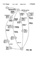
- FIG. 1 is a block diagram of a hand-held computer system according to the preferred embodiment of the present invention
- FIGS. 2A and 2B are a state diagram of a state machine that controls the capture of flash command bytes through the parallel port of the computer system of FIG. 1;
- FIG. 3 is a logic diagram of circuitry that interfaces with signals provided to and by the state machine of FIGS. 2A and 2B;
- FIGS. 4A and 4B are a logic diagram of circuitry used to capture the flash command bytes
- FIG. 5 is a state diagram of a state machine that performs a boundary scan tristate cycle to seize control of the system bus;
- FIG. 6 is a logic diagram of circuitry that interfaces with signals provided to and by the state machine of FIG. 5;
- FIG. 7 is a logic diagram of circuitry for decoding the flash command bytes to determine the type of command requested
- FIGS. 8A and 8B are a logic diagram of an address counter, a byte counter, and a word counter that provides the addresses to flash memory devices in the computer system of FIG. 1, keeps track of the number of bytes transferred through the parallel port in the computer system, and keeps track of the number of words provided over the computer system bus, respectively;
- FIGS. 9A and 9B are a state diagram of a state machine that performs handshaking functions with an external computer connected to the parallel port of the computer system of FIG. 1;
- FIGS. 10A and 10B are a logic diagram of circuitry that interfaces with signals provided to and by the state machine of FIGS. 9A and 9B;
- FIGS. 11A-11C are a state diagram of a state machine that controls the read and write to the flash memory devices located in the computer system of FIG. 1;
- FIG. 12 is a state diagram of a state machine that controls the input signal timings to the flash memory devices located in the computer system of FIG. 1;
- FIGS. 13A and 13B are a logic diagram of circuitry that interfaces with the signals provided to and by the state machines of FIGS. 11A-11C and 12;
- FIGS. 14A and 14B are a logic diagram of a multiplexor selecting the proper data signals to be provided to the system bus of the computer system of FIG. 1;
- FIGS. 15A and 15B are a logic diagram of a multiplexor selecting the proper output byte to be provided to the parallel port of the computer system of FIG. 1.
- a central processing chipset 100 which includes an integrated processor controller (IPC) 102 and a multiple peripheral controller (MPC) 104, is connected to a system bus 106 having a data bus SD, an address bus SA and a control bus SC.
- the integrated processor controller or IPC 102 includes a CPU 108, preferably a 32-bit 386SL microprocessor from Intel Corporation.
- the CPU 108 can be operated at 3.3 volts for low power consumption or at 5 volts for higher performance.
- the preferred embodiment of the computer system C is a hand-held system, the CPU 108 and the rest of the system is powered at 3.3 volts for maximum power efficiency.
- the IPC 102 also includes a non-volatile memory controller 112, as well as an ML bus controller 114 to interface with PCMCIA slot controllers 116, which are connected to the ML bus.
- the ML bus and system address bus SA are multiplexed on the same physical lines to save routing space.
- the IPC 102 also contains a video controller for controlling an LCD display (not shown) connected through an LCD connector 132.
- a bank of memory 148 is connected to the IPC 102 via a memory bus 152.
- the bank of memory 148 preferably implemented with 2 Mbytes of DRAM chips, is used as both main and video memory.
- the multiple peripheral controller or MPC 104 is also connected to the system bus 106.
- the MPC 104 provides an interface to a parallel port 124, a serial port 134, a keyboard 120 and a speaker 122.
- the MPC 104 includes a real-time clock (RTC), which provides various real-time clock functions, and an extended CMOS memory to provide storage for various system configuration information.
- RTC real-time clock
- the hand-held computer system C utilizes a pen as the primary input device.
- a digitizer grid 130 is used to interface the pen to an auxiliary microcontroller 128, which is connected to the MPC 104 via a serial link into a special UART input of the MPC 104.
- the auxiliary microcontroller 128 is also connected to a DC/DC power converter 138.
- the auxiliary microcontroller 128 is used for such other functions as battery charge control and termination, and power supply control and supervision.
- the DC/DC converter 138 is connected between the MPC 104 and a battery 140.
- An enhanced parallel port (EPP) controller 142 is connected between the parallel port 124 and the system bus 106.
- the EPP controller 142 is connected to the parallel port 124 via a parallel port bus 125, which includes a parallel port data bus PD 7:0! and status signals.
- the EPP controller 142 is used to control transfer of data between the parallel port 124 and an external host device (not shown) connected to the parallel port 124.
- an external host computer is utilized, but other devices could be utilized.
- the data is transferred between the host computer and the hand-held computer system C according to the Enhanced Parallel Port (EPP) communications protocol described in the IEEE 1284 specification, Standard Signaling Method for a Bi-directional Parallel Peripheral Interface for Personal Computers, IEEE STD 1284-XXXX (Feb. 1, 1993), which is hereby incorporated by reference.
- the EPP controller 142 can be used with either bi-directional or uni-directional parallel ports.
- the EPP controller 142 includes a mode register 143.
- the mode register 143 indicates one of three modes: a hardware mode, a software slave mode, and a software master mode.
- a hardware mode which is indicated by a signal HW -- MODE being asserted high
- the transfer of data between the host computer and the hand-held computer system C is controlled exclusively by the EPP controller 142.
- software slave mode which is indicated by a signal SW -- SLAVE being asserted high
- the software master mode allows the EPP controller 142 to communicate with another hand-held computer system C, as long as that other system is in software slave mode.
- the hand-held computer system C also includes two banks (banks 0 and 1) of flash EEPROMs 144 to store the operating system.
- the total size of the flash EEPROMs 144 is preferably 4 Megabytes (MB), implemented with 4 1M ⁇ 8 flash EEPROM chips.
- each bank of the flash EEPROMs 144 contains two 1M ⁇ 8 flash memory chips.
- Additional storage capacity in the form of a resident flash array (RFA) 146 is also provided with the computer system C.
- the RFA 146 is also implemented with two banks (banks 2 and 3) of flash EEPROMs, which are connected to the system bus 106.
- the RFA 146 is used as a mass storage device for storage of system and user data.
- the total capacity of the RFA 146 is preferably 4 MB, although additional flash memory devices can be added to increase the storage capacity to 12 MB.
- the RFA 146 is also expandable with flash memory cards inserted through the PCMCIA slots 116.
- a brief description of IEEE 1284 status signals provided through the parallel port 124 is provided here to assist the understanding of the operations of the EPP controller 142.
- the EPP controller 142 is assumed to be in EPP mode for this description.
- a signal NSTROBE is used to denote an address or data read or write operation between the host and a peripheral device such as the hand-held computer system C in the case of the preferred embodiment. If the signal NSTROBE is asserted low, then a write is indicated; if high, a read is indicated. Address and data signals are transferred through a parallel port data bus PD 7:0!.
- a signal NACK is used by the hand-held computer system C to interrupt the host computer. The rising edge of the signal NACK causes the interrupt.
- a signal BUSY is used by the hand-held computer system C to notify the host computer that a data or address transfer has been completed and that the hand-held computer C is ready for the next cycle.
- a signal NAUTOFD when asserted low by the host computer, denotes that a data cycle is taking place.
- a signal NINIT when asserted low by the host computer, initiates a termination cycle to return the EPP controller 142 to the compatible mode, which is an IEEE 1284 mode in which the host to peripheral communication is done via the traditional uni-directional interface. As will be discussed below, asserting the signal NINIT causes the EPP controller 142 to exit from the EPP mode, thereby halting the data transfer between the host computer and the hand-held computer system C.
- a signal NSELECTIN when asserted low by the host computer, denotes an address cycle.
- an IEEE 1284 compliant host computer To communicate with the hand-held computer system C, an IEEE 1284 compliant host computer first enters into a negotiation cycle with the hand-held computer system C. The host computer verifies that the hand-held computer system C is IEEE 1284 compliant by monitoring signals PERROR and NFAULT through the parallel port 124, which must both be at logic high levels. After verifying that the hand-held computer system C is IEEE 1284 compliant, the host computer requests one of a plurality of communications modes provided by the IEEE 1284 specification, which includes the EPP mode. The EPP mode is requested by placing an extensibility value of 0 ⁇ 40 on the parallel port data bus PD 7:0! at the beginning of the negotiation phase. The EPP mode provides asymmetric bi-directional data transfers between the host computer and the hand-held computer system C. For a more detailed description of the EPP communications mode, refer to the IEEE 1284 Specification.
- the host computer provides additional information to the EPP controller 142 without violating the IEEE 1284 standard.
- the additional information preferably consists of two flash command bytes, which include a starting bank number, a block number, the type of command cycle to be performed on the flash EEPROMs 144 or 146, and an ending bank number.
- the starting and ending bank numbers refer to which bank or banks of the flash EEPROMs 144 and 146 are to be accessed.
- the block number designates the particular block in each of the flash EEPROMs 144 or 146 on which the specified command is to be performed.
- the EPP controller 142 issues a boundary scan tristate cycle on the system bus 106 to seize control of the system bus 106. Until the EPP controller 142 obtains control of the system bus 106, it blocks all transfers from the host computer by not responding to any read or write requests. Once the boundary scan tristate cycle has completed, the EPP controller 142 accepts transfer requests from the host computer. Communications between the EPP controller 142 and the flash EEPROMs 144 and 146 are accomplished over the system data bus SD and address bus SA, as well as other control signals.
- the control signals include four chip select signals CS0*-CS3*, a read signal MEMRD, a write signal MEMWR*, and a signal VPP -- SW that causes the DC/DC converter 138 to activate the 12-volt VPP inputs of the flash EEPROMs 144 or 146 for erasing or programming.
- FIGS. 2A and 2B a state diagram is shown of a state machine FSTATE in the EPP controller 142 that controls the capture of the flash command bytes provided by the host computer.
- the inputs to the state machine FSTATE are state signals FSTATE 3:0! and signals SNSELECTIN, SNAUTOFD, SNINIT, RESET, ERROR, BDONE, PD -- IN 7:0! and TO2.
- the outputs of the state machine FSTATE are state signals FSTATE -- D 3:0! and signals RST -- TMR -- W, FLASH -- W, TS and CMD -- SB.
- the parallel port data bus PD 7:0! is provided to input buffers (not shown) in the EPP controller 142.
- the buffered signals are represented as signals PD -- BUF 7:0!.
- the buffered parallel port data input signals PD -- BUF 7:0! are double buffered through two registers 348 and 350 to generate latched data inputs PD -- IN 7:0!.
- the registers 348 and 350 are clocked on the rising edge of CLK14M, a 14 MHz clock signal, and reset by the signal RESET.
- the data provided by the host computer onto the parallel port data bus PD 7:0! is asynchronous to the clock CLK14M, and thus must be double buffered to ensure that the EPP controller 142 receives valid data from the host computer.
- the signal SNAUTOFD is provided by a D flip-flop 306, whose D input is connected to the parallel port status signal NAUTOFD.
- the signal SNSELECTIN is provided by a D flip-flop 310, whose input is connected to the output of another D flip-flop 308.
- the D input of the D flip-flop 308 is connected to the parallel port status signal NSELECTIN.
- the signal SNINIT is provided by a D flip-flop 312, whose D input is connected to the parallel port status signal NINIT.
- the D flip-flops 306, 308, 310 and 312 are all clocked by CLK14M. All of the D flip-flops 306, 308, 310 and 312 are reset on the rising edge of the system reset signal RESET.
- the parallel port signals NSELECTIN, NINIT, and NAUTOFD are latched through the D flip-flops to synchronize them to the clock CLK14M.
- the signal SNINIT is connected to the input of an inverter 314, which drives a signal ABORT.
- the parallel port status signal NINIT when asserted low, initiates a termination cycle. This causes the signal SNINIT to be asserted low, and the signal ABORT to be asserted high, on the next rising edge of the clock CLK14M.
- the timeout signal TO2 is provided by a comparator 320, which compares the output of a counter 318 with the value 0 ⁇ FFFF.
- the timeout signal TO2 is asserted high whenever the counter 318 counts to the value 0 ⁇ FFFF.
- the clock input of the counter 318 is connected to the output of an AND gate 316.
- the first input of the AND gate 316 is connected to the clock CLK14M and its second input is connected to the inverted state of the timeout signal TO2.
- the reset input of the counter 318 is connected to the output of an OR gate 322, whose inputs are connected to a signal RST -- TMR and the system reset signal RESET. When either of these signals is asserted high, the counter 318 is reset to the value 0.
- the signal FLASH -- W is provided by the state machine FSTATE to the 1 input of a multiplexor 326, whose output is connected to the D input of a D flip-flop 334.
- the 0 input of the multiplexor 326 is connected to the output of a multiplexor 324.
- the output of the D flip-flop 334 is connected to a signal FLASH, which is connected to the 0 input of the multiplexor 324.
- the signal FLASH indicates to the other portions of the EPP controller 142 that the flash EEPROMs 144 or 146 are being accessed through the parallel port 124.
- the 1 input of the multiplexor 324 is tied low.
- the select input of the multiplexor 326 is connected to the output of an AND gate 332, whose inputs are connected to the output of a comparator 328 and the output of a comparator 330. If the state machine FSTATE is in state CST5 and the parallel port data inputs PD -- IN 7:0! contain the value 0 ⁇ 40, then the AND gate 332 causes the multiplexor 326 to select the signal FLASH -- W to latch into the D flip-flop 334. Otherwise, the multiplexor 326 selects the output of the multiplexor 324, whose select input is connected to the output of an OR gate 336.
- the inputs of the OR gate 336 are connected to the timeout signal TO2 and the signal ERROR, which indicates that the flash command bytes latched by the EPP controller 142 are erroneous. If either of the signals TO2 or ERROR is asserted high, the multiplexor 324 selects the value 0. Otherwise the output of the D flip-flop 334 is selected. Thus, if the state machine FSTATE is in state CST5 and the value of the parallel port bus PD -- IN 7:0! contains the value 0 ⁇ 40, then the signal FLASH -- W is latched into the D flip-flop 334. Otherwise, the signal FLASH is deasserted low if either the signal TO2 or ERROR is asserted high and remains unchanged otherwise.
- the signal RST -- TMR -- W is connected to the D input of a D flip-flop 304, which is clocked by the clock CLK14M.
- the output of the D flip-flop 304 is connected to the signal RST -- TMR, which when asserted resets the counter 318.
- the D flip-flop 304 is reset by the signal RESET.
- the state machine FSTATE enters into state RST from any other state if the signal RESET is asserted high or if the signal RESET is deasserted low and the signal SNINIT is asserted low.
- state RST the signal RST -- TMR -- W is asserted high.
- the state machine FSTATE transitions from state RST to state CST0 if the following condition is true: the signals SNSELECTIN and SNINIT are high, the signals SNAUTOFD and RESET are low and the data inputs PD -- IN 7:0! contain the value 0 ⁇ 40.
- This condition represents the IEEE 1284 negotiation cycle, which is initiated by the host computer to request an EPP communications mode.
- state CST0 if the states of the signals SNSELECTIN, SNAUTOFD, SNINIT, RESET and PD -- IN 7:0! remain unchanged and the timeout signal TO2 transitions high to indicate that no activity has occurred in 64K (0 ⁇ FFFF) CLK14M cycles, the state machine FSTATE transitions from state CST0 to state STOP. The state machine remains in state STOP until either the reset signal RESET is asserted high or the termination initiation signal SNINIT is asserted low, whereupon the state machine FSTATE transitions back to state RST. With the transition from state CST0 to state STOP, the signal RST -- TMR -- W is asserted high.
- the signals SNSELECTIN and SNINIT are assumed to be high and the signals SNAUTOFD and RESET are assumed low unless otherwise specified. As noted earlier, this condition indicates a negotiation cycle. If the timeout signal TO2 remains deasserted, the state machine stays in state CST0 if any one of the following conditions is true: the value of the data inputs PD -- IN 7:0! is equal to the value 0 ⁇ 40, the bit PD -- IN 7! is low, the bit PD -- IN 6! is high, the bit PD -- IN 5! is low, the bit PD -- IN 4! is high, the bit PD -- IN 3! is low, the PD -- IN 2! is low, the bit PD -- IN 1! is high or the bit PD -- IN 0! is high.
- the state machine FSTATE transitions from state CST0 to state CST1. With the transition, the signal RST -- TMR -- W is asserted high. By placing the value 0 ⁇ AC on the parallel port bus PD 7:0!, the host computer is signaling to the EPP controller 142 that flash command bytes will follow. Once in state CST1, if the timeout signal TO2 is asserted high and the error signal ERROR is deasserted low or if the signal ERROR is asserted high, then the state machine transitions from state CST1 to STOP. The signal RST -- TMR -- W is asserted high with the transition.
- the bit PD -- IN 7! corresponds to a clock bit provided by the host computer. If the clock bit PD -- IN 7! is asserted high and the signals ERROR and TO2 are low, then the state machine stays in state CST1, with all the output signals being deasserted low.
- the host computer asserts the clock bit PD -- IN 7! high. If the signals ERROR and TO2 remain deasserted low, then the state machine transitions from state CST2 to state CST3, asserting the output signal RST -- TMR -- W high. The transition to state CST3 causes the EPP controller 142 to latch in the first flash command byte.
- state CST3 if the clock bit PD -- IN 7! remains high and either of the signals ERROR or TO2 are asserted high, then the state machine FSTATE transitions from state CST3 to state STOP. However, if the signals ERROR and TO2 remain low and the clock bit PD -- IN 7! remains high, then the state machine stays in state CST3.
- the state machine FSTATE transitions from CST3 to state CST4 when the clock bit PD -- IN 7! is deasserted low and the signals ERROR and TO2 remain low.
- the clock bit PD -- IN 7! deasserted low indicates that the host computer is placing the second flash command byte on the parallel port data bus PD -- IN 7:0!. With the transition from state CST3 to state CST4, the signal RST -- TMR -- W is asserted high.
- state machine FSTATE transitions to state STOP if either of the signals ERROR or TO2 are asserted high.
- the signal RST -- TMR -- W is asserted high with the transition.
- the state machine stays in state CST4. If the clock bit PD -- IN 7! is asserted high and the signals ERROR and TO2 remain low, then the state machine transitions from state CST4 to state CST5. This causes the second flash command byte to be latched into the EPP controller 142.
- the signal RST -- TMRW is asserted high with the transition.
- state machine transitions to state STOP if the clock bit PD -- IN 7! is high and either of the signals ERROR or TO2 is also asserted high.
- the signal RST -- TMR -- W is asserted high with the transition.
- the state machine remains in state CST5 if the signals ERROR and TO2 both remain low and one of the following conditions is true: the bit PD -- IN 7! is high, the bit PD -- IN 6! is low, the bit PD -- IN 5! is high, the bit PD -- IN 4! is high, the bit PD -- IN 3! is high, the bit PD -- IN 2! is high, the PD -- IN 1! is high or the bit PD -- IN 0! is high.
- the state machine FSTATE remains in state CST5 until the host computer places the value 0 ⁇ 40 back onto the parallel port data bus PD 7:0!. While in state CST5, all of the output signals of the state machine FSTATE are deasserted low.
- the state machine transitions from state CST5 to state CST6 when the value of the latched data inputs PD -- IN 7:0! is changed to the value 0 ⁇ 40.
- the state machine waits in state CST6 until the signal BDONE is asserted high to indicate that other bus masters on the system bus 106 have relinquished control of the system bus 106, and that the EPP controller 142 has seized control of the system bus 106.
- the state machine remains in state CST6 if the signals ERROR, BDONE, and TO2 are low and the latched data inputs PD -- IN 7:0! contain the value 0 ⁇ 40.
- the signals RST -- TMR -- W , FLASH -- W and TS are asserted high.
- the signal FLASH -- W is latched to produce the signal FLASH, which indicates to the other portions of the EPP controller 142 that an access to the flash EEPROMs 144 or 146 is about to occur.
- the signal TS when asserted high, causes a state machine BSCAN (FIG. 5) to issue a boundary scan tristate cycle to allow the EPP controller 142 to seize control of the system bus 106.
- the state machine FSTATE transitions to state STOP if the signals ERROR and TO2 remain low and the data inputs PD -- IN 7:0! contain the value 0 ⁇ 40.
- the signals RST -- TMR -- W , FLASH -- W and CMD -- SB are asserted high with the transition.
- the signal CMD -- SB causes decoding of the latched flash command bytes to generate one of a plurality of signals to indicate the type of command cycle to be executed.
- Capture signals CAPTURE0, CAPTURE1, CAPTUREA0 and CAPTUREA1 are all pulsed signals.
- the signal CAPTURE0 is generated by the combination of a comparator 400, D flip-flops 402, 404 and 406, and an AND gate 408. If the comparator 400 determines that the state machine FSTATE is in state CST3, it latches a high into the D flip-flop 402 on the rising edge of the clock CLK14M. On the next rising edge of the clock CLK14M, the high state is latched into the D flip-flop 404.
- the output of the D flip-flop 404 is connected to the first input of the AND gate 408, whose other input is connected to the inverted state of the output of the D flip-flop 406.
- the AND gate 408 asserts the signal CAPTURE0 high.
- the high value from the comparator 400 is latched into the D flip-flop 406, at which point the signal CAPTURE0 is deasserted low.
- the signal CAPTURE0 is pulsed high for one CLK14M cycle.
- the signal CAPTURE1 is generated in a similar manner by the combination of a comparator 410, D flip-flops 412, 414 and 416, and an AND gate 418. If the state machine FSTATE is in state CST5, the comparator 410 outputs a high state. The signal CAPTURE1 is also pulsed high for one CLK14M cycle.
- the signal CAPTUREA0 is pulsed high by the combination of a comparator 420, D flip-flops 422 and 424, and an AND gate 426. If the state machine FSTATE is in state CST2, the comparator 420 outputs a high. The output of the comparator 420 is connected to the D input of the D flip-flop 422, which is clocked by CLK14M. On the next rising edge of the clock CLK14M, the high state provided by the comparator 420 is latched into the D flip-flop 422. The output of the D flip-flop 422 is provided to the first input of the AND gate 426 and also to the D input of the flip-flop 424.
- the other input of the AND gate 426 is connected to the inverted state of the output of the D flip-flop 424.
- the signal CAPTUREA0 is asserted high by the AND gate 426.
- the D flip-flop 424 latches in the high value.
- the signal CAPTUREA0 is deasserted low.
- the signal CAPTUREA1 is pulsed high in a similar fashion by the combination of a comparator 428, D flip-flops 430 and 432, and an AND gate 434.
- the signal CAPTUREA1 is pulsed high for one CLK14M cycle when the state machine FSTATE reaches state CST4.
- the D flip-flops 402-406, 412-416, 422 and 424, and 430 and 432 are all reset low when the signal RESET is asserted high.
- the latched parallel port data inputs PD -- IN 6:0! are provided to the 1 input of a multiplexor 436.
- the 0 input of the multiplexor 436 is connected to the output of a register 440, which is connected to signals FCMD 6:0!.
- the signals FCMD 6:0! represent the 7 lower bits of the first flash command byte.
- the select input of the multiplexor 436 is connected to the signal CAPTURE0.
- the output of the multiplexor 436 is connected to the 0 input of a multiplexor 438, whose 1 input is tied low.
- the output of the multiplexor 438 is connected to the input of the register 440, and the select input of the multiplexor 438 is connected to the output of a comparator 441.
- the comparator 441 determines if the state machine FSTATE is in state CST1.
- the register 440 is clocked by CLK14M and reset by the signal RESET.
- the comparator 441 asserts a high output, causing the multiplexor 438 to select the value 0 to latch into the register 440.
- the register 440 is thus initialized to the value 0 whenever the state machine FSTATE transitions to state CST1 in response to a negotiation cycle. If the state machine FSTATE is not in state CST1, then the output of the multiplexor 436 is selected.
- the multiplexor 436 selects the signals FCMD 6:0! if the signal CAPTURE0 is low, keeping the state of signals FCMD 6:0! unchanged.
- the multiplexor 436 selects the parallel port data inputs PD -- IN 6:0! if the signal CAPTURE0 is asserted high.
- the first command byte is latched into the register 440 when the signal CAPTURE0 is asserted high.
- the second flash command byte is latched into a register 446 and provided onto signals FCMD 14:8! if the signal CAPTURE1 is asserted high.
- the data inputs PD -- IN 6:0! are connected to the 1 input of a multiplexor 442.
- the 0 input of the multiplexor 442 is connected to the signals FCMD 14:8!.
- the select input of the multiplexor 442 is connected to the signal CAPTURE1.
- the output of the multiplexor 442 is connected to the 0 input of a multiplexor 444, whose 1 input is tied low.
- the output of the multiplexor 444 is connected to the input of the register 446, which is clocked by CLK14M and reset by the signal RESET.
- the select input of the multiplexor 444 is connected to the output of the comparator 441.
- the state machine FSTATE is in state CST1
- the value 0 is latched into the register 446.
- the signal CAPTURE1 is deasserted low, the signals FCMD 14:8! remain unchanged.
- the signal CAPTURE1 is asserted high, indicating that the state machine FSTATE has reached state CST5
- the data inputs PD -- IN 6:0! are latched into the register 446.
- the state of the data inputs PD -- IN 6:0! are also latched into registers 454 and 458 (FIG. 4B) in states CST2 and CST4, respectively. These values are compared to the values obtained in states CST3 and CST5 to ensure that no error has occurred.
- the host computer places valid first and second flash command bytes onto the parallel port data bus PD 7:0! during states CST2 and CST4, respectively. Comparing the values latched in states CST2 and CST4 with the values latched in states CST3 and CST5, respectively, ensures that the flash command bytes have been held long enough to satisfy hold time requirements.
- the state of the parallel port data inputs PD -- IN 6:0! is latched into the registers 454 and 458, whose outputs are represented by signals TP0 6:0! and TP1 6:0!, respectively.
- the data inputs PD -- IN 6:0! are connected to the 1 input of a multiplexor 452, whose output is connected to the input of the register 454.
- the select input of the multiplexor 452 is connected to the signal CAPTUREA0, and its 0 input is connected to the signals TP0 6:0!.
- the state of the data inputs PD -- IN 6:0! is latched into the register 454. Otherwise, the state of the signals TP0 6:0! remain unchanged.
- the data inputs PD -- IN 6:0!0 are connected to the 1 input of a multiplexor 456, whose output is connected to the input of the register 458.
- the select input of the multiplexor 456 is connected to the signal CAPTUREA1, and the 0 input of the multiplexor 456 is connected to the signals TP1 6:0!.
- Both registers 454 and 458 are clocked by CLK14M and reset by the signal RESET.
- the signals TP0 6:0! are compared to the values of the data inputs PD -- IN 6:0! by a comparator 460.
- the output of the comparator 460 is connected to the 1 input of a multiplexor 462, whose output is connected to the 0 input of a multiplexor 464.
- the 0 input of the multiplexor 462 is connected to the output of a D flip-flop 466, which is connected to a signal CMD -- ERR0.
- the D flip-flop 466 is clocked by CLK14M and reset by the signal RESET.
- the select input of the multiplexor 462 is connected to the signal CAPTURE0.
- the 1 input of the multiplexor 464 is tied low and its select input is connected to the output of the comparator 441, which determines if the state machine FSTATE is in state CST1. If the state machine FSTATE is in state CST1, the multiplexor 464 selects the value 0 to latch into the D flip-flop 466 to initialize the signal CMD -- ERR0 low. Otherwise, if the signal CAPTURE0 is low, the state of the D flip-flop 466 remains unchanged. If the signal CAPTURE0 is high, indicating that the first flash command byte is being latched into the register 440, a comparison is made between the signals TP0 6:0! and the latched parallel port data inputs PD -- IN 6:0!.
- the comparator 460 If the values are not equal, then the comparator 460 outputs a high, which is latched into the D flip-flop 466 through the multiplexors 462 and 464.
- the output of the D flip-flop 466 is connected to the first input of an OR gate 480, whose output is connected to the signal ERROR.
- the second flash command byte is compared in a similar fashion by the combination of a comparator 470, multiplexors 472 and 474, and a D flip-flop 476.
- the D flip-flop 476 is clocked by CLK14M and reset by the signal RESET. If the value of the signals TP1 6:0! is not equal to the value of the latched data inputs PD -- IN 6:0! when the signal CAPTURE1 is asserted high, then the comparator 470 asserts a high, which is latched into the D flip-flop 476 through the multiplexors 472 and 474 on the rising edge of the clock CLK14M.
- the output of the D flip-flop 476 is connected to a signal CMD -- ERR1, which is connected to the second input of the OR gate 480.
- the D flip-flop 476 is also initialized to the value 0 when the state machine FSTATE reaches state CST1. Thus, if either the first flash command byte or second flash command byte does not produce a match, then the signal ERROR is asserted high by the OR gate 480 to indicate an error.
- the flash command bits FCMD 15:0! contain the following information.
- Bits FCMD 15! and FCMD 7! are clock bits used by the host computer to clock the flash command bytes into the EPP controller 142.
- the bits FCMD 6:5! determine the starting bank number, which can be one of the values 0-3.
- Bits FCMD 3:0! represent the block in the selected bank of flash memory.
- Each bank of the flash EEPROMs 144 and 146 contains 16 blocks, in which each block contains 64K bytes.
- bits FCMD 14:12! contain the encoded value of the flash command.
- Available flash commands include a write command, a read command, a block erase command, a clear status register command, a read ID command and a parallel port disable command for the value of bits FCMD 14:12! equal to 1, 2, 3, 4, 5 and 6, respectively.
- Bits FCMD 11:10! are reserved for future expansion.
- bits FCMD 9:8! represents the ending bank number of the flash memory.
- the host computer switches the value of the parallel port bus PD 7:0! back to the value 0 ⁇ 40.
- This causes the state machine FSTATE to transition to state CST6 and to assert the signal TS high.
- the asserted signal TS causes the state machine BSCAN (FIG. 5) in the EPP controller 142 to issue a boundary scan tristate command to the IPC 102 so that the enhanced parallel port controller 142 can seize control of the system bus 106.
- the EPP controller 142 Before it obtains control of the system bus 106, the EPP controller 142 is not ready to receive data from the host computer. As a result, the EPP controller 142 blocks all transfers from the host computer by not responding to any read or write requests from the host computer.
- the inputs to the state machine BSCAN are state signals BSTATE 3:0! and signals TS, COUNT7, RESET and EPP -- REL.
- the signal EPP -- REL is provided by a comparator 340 in FIG. 3. If the comparator 340 determines that the state machine FSTATE is in state STOP, then the signal EPP -- REL is asserted high.
- the outputs of the state machine BSCAN are state signals BSTATE -- D 3:0! and signals TMS, CNTR -- ON, SHIFT -- ON, BDONE and BSC -- EN -- W.
- a system reset indicated by asserting the signal RESET high, causes the state machine BSCAN to enter into its initial state B0. With this transition, the signal TMS is asserted high. The state machine BSCAN stays in state B0 while the signal TS is low and the signal RESET is low. The signal TMS is maintained high.
- the state machine BSCAN begins the boundary scan tristate cycle on the system bus 106.
- the state machine BSCAN transitions from state B0 to B1, asserting the signal BSC -- EN -- W high.
- the signal BSC -- EN -- W causes output tristate buffers that drive the signals TMS and TDO to be enabled.
- the signals TMS and TDO are used to transmit the tristate command to other bus masters using the boundary scan protocol.
- the CPU 108 is the only other bus master that contains the boundary scan test logic.
- the signal TMS is provided to other bus masters to select the desired test operation.
- the signal TDO is a serial output for test instructions and data, which are provided to the boundary scan test serial input of the CPU 108.
- the CPU 108 includes a shift register into which data on the shift input is fed. The data in the shift register is then loaded into a test data register or test instruction register as appropriate.
- the state machine BSCAN If the signal TS is deasserted low when the state machine BSCAN is in state B1, it stays in state B1, maintaining the signal BSC -- EN -- W asserted high. However, if the signal TS is maintained high, the state machine BSCAN transitions from state B1 to B2, asserting the signals TMS and BSC -- EN -- W high. From state B2 the state machine transitions to state B3. The signals TMS and BSC -- EN -- W are maintained high. Asserting the signal TMS high over two clock periods places the test logic in the CPU 108 in a condition ready to accept a new test instruction. Next, the state machine transitions from state B3 to B4. With this transition, the signal TMS is deasserted low, but the signal BSC -- EN -- W is maintained high.
- state machine transitions to state B5, keeping the signal BSC -- EN -- W asserted high.
- the state machine then transitions from state B5 to B6.
- the signals CNTR -- ON and BSC -- EN -- W are asserted high with this transition.
- the signal TMS is maintained low.
- the test logic in the CPU 108 is ready to shift data into the shift register.
- the signal CNTR -- ON enables the clock input of a three-bit counter 604, which is described below in FIG. 6.
- the state machine BSCAN stays in state B6 until the counter 604 reaches a predetermined value, as indicated by the signal COUNT7. Thus, if the signal COUNT7 is deasserted low, the state machine stays in state B6.
- the signals CNTR -- ON and BSC -- EN -- W are maintained high and the signal SHIFT -- ON is asserted high.
- the signal SHIFT -- ON causes the value 0b1101 to be serially shifted onto the signal TDO. This value is in turn shifted into the shift register of the CPU 108 through its test serial input.
- the signal COUNT7 is asserted high and the state machine transitions from state B6 to state B7. With this transition, the signals TMS, CNTR -- ON, SHIFT -- ON and BSC -- EN -- W are all asserted high. Assertion of the signal TMS causes the test logic in the CPU 108 to stop shifting data into its shift register. From state B7, the state machine transitions to state B8 while maintaining the signals TMS and BSC -- EN -- W high. Maintaining the signal TMS high causes the instruction in the shift register to be loaded into the test instruction register of the CPU 108. This instruction is the tristate command, which causes the CPU 108 to tristate its pins to enable the EPP controller 142 to gain control of the bus 106.
- the state machine BSCAN transitions from state B8 to B9.
- the signals BDONE and BSC -- EN -- W are asserted high with the transition.
- the signal BDONE indicates that the boundary scan cycle has completed.
- the state machine BSCAN remains in state B9 until the state machine FSTATE transitions from state CST6 to state STOP.
- the signal EPP -- REL is asserted high, the state machine BSCAN transitions from state B9 to state B1.
- the signal BSC -- EN -- W is maintained high.
- the inputs of an AND gate 602 are connected to the inverted state of the signal EPP -- REL, and to the signal CNTR -- ON and the clock CLK14M.
- the output of the AND gate 602 is connected to the clock input of a three-bit counter 604, whose output is connected to signals COUNT 2:0!.
- the counter 604 is reset to the value 0 when the signal RESET is asserted high.
- the signals COUNT 2:0! are connected to one input of a comparator 606, which compares the value of COUNT 2:0! to the value 3. If a match occurs, the comparator 606 asserts the signal COUNT7 high.
- the state signals BSTATE -- D 3:0! provided by the state machine BSCAN are connected to the input of a register 608, which is clocked by CLK14M.
- the output of the register 608 is connected to state signals BSTATE 3:0!.
- the register 608 is reset to the value 0 ⁇ 0 on the rising edge of the signal RESET.
- the signal BSC -- EN -- W is connected to the D input of a D flip-flop 610, which is clocked on the falling edge of CLK14M.
- the output of the D flip-flop 610 is connected to the signal BSC -- EN.
- the signal BSC -- EN is provided directly to enable the tristate buffers (not shown) driving the signals TMS and TDO.
- the D flip-flop 610 is reset by a signal RESET1, which is provided by a D flip-flop 612.
- the D input of the D flip-flop 612 is connected to the signal RESET, and it is clocked on the rising edge of CLK14M.
- the signal SHIFT -- ON is connected to one input of an AND gate 614.
- the second input of the AND gate 614 is connected to the inverted state of the signal CLK14M.
- the output of the AND gate 614 is connected to the clock input of a 4-bit shift register 616.
- the least significant bit of the shift register 616 is connected to a signal TDO, which is wrapped around and connected to the most significant bit of the 4-bit shift register 616.
- the shift register 616 is reset to the value 0b1101.
- the shift register 616 works in conjunction with the counter 604. While the state machine BSCAN is in state B6, the signal CNTR -- ON is asserted high to enable the counter 604, and the signal SHIFT -- ON is asserted to enable the shift register 616. The state machine BSCAN remains in state B6 until the counter 604 counts to the value 3. This allows the shift register 616 to serially output the value 0b1101 through the signal TDO.
- the EPP controller 142 After the boundary scan tristate cycle has been successfully completed, as indicated by the signal BDONE being asserted high, the EPP controller 142 is ready to accept write and read cycles from the host computer.
- the EPP controller 142 interfaces with the flash EEPROMs 144 and 146 through the system data bus SD 15:0! and the system address bus SA 20:1!.
- four select signals CS0, CS1, CS2, and CS3, are provided to select banks 0, 1, 2 and 3, respectively, of the flash EEPROMs 144 and 146.
- a write to the flash EEPROMs 144 and 146 is indicated by a signal MEMWR*, which is connected to the write enable inputs of the flash EEPROMs 144 or 146.
- a read from the flash EEPROMs 144 and 146 is indicated by a signal MEMRD*, which is connected to output enable inputs of the flash EEPROMs 144 or 146.
- a signal VPP -- SW is provided to the DC/DC converter 138 to activate the 12-volt VPP inputs to the flash EEPROMs 144 and 146.
- the 12-volt VPP supply voltage is needed to erase or program the flash EEPROMs 144 or 146.
- the flash EEPROMs 144 and 146 provide a signal RY to indicate if they are ready for the next command operation.
- the commands recognized by a flash memory device includes a read ID operation, a read status register operation, an erase operation, a clear status register, a write operation and a read array operation.
- the read ID operation allows the host computer to access the manufacturer code and device code of the flash EEPROMs 144 and 146 so that the host computer can automatically match the devices with their proper block erase and write algorithms.
- the read ID cycle is initiated by writing the value 0 ⁇ 90 into a command user interface located in each of the flash EEPROMs 144 and 146. Following the command write, a read cycle from address 0 ⁇ 00000 retrieves the manufacturer code and a read cycle from address 0 ⁇ 00001 returns the device code.
- the read array command is initiated by writing the value 0 ⁇ FF into the command user interface.
- the flash EEPROMs 144 and 146 remain enabled for reads until the contents of the command user interface are changed.
- an entire 64K block of the selected bank of the flash EEPROMs 144 or 146 is accessed in a read array operation.
- an address counter 800 (FIG. 8) is provided that increments the starting block address 64K times.
- Each flash memory device contains a status register which may be read to determine when a write or block erase operation has completed successfully.
- the read status register operation is initiated by writing the value 0 ⁇ 70 to the command user interface. Any subsequent read operation outputs data from the status register.
- the status register is an 8-bit register. The most significant bit, or bit 7, of the register generates the signal RY.
- Bit 6 of the status register indicates whether an erase operation has been suspended. An erase operation can be suspended to allow data to be read from another block of the flash memory.
- Bit 5 of the status register also represented as a signal ERASE -- ERR, indicates whether an error has occurred during a block erase operation.
- Bit 4 also represented as a signal WRITE -- ERR, indicates whether an error has occurred during a write operation.
- Bit 3 also represented as a signal VPP -- ERR, indicates whether the voltage level of the VPP voltage input is below a predetermined threshold value.
- a clear status register command is asserted to reset the erase and write status bits of the status register.
- the clear status register operation is initiated by writing the value 0 ⁇ 50 to the command user interface.
- the block erase operation is executed to one 64k block of the flash memory device at a time and is initiated by a two-cycle command sequence.
- the first cycle is an erase setup command, which is initiated by writing the value 0 ⁇ 20 to the command user interface.
- the second cycle is an erase confirm command, which is asserted by writing the value 0 ⁇ D0 to the command user interface.
- the write operation is also executed by a two command sequence.
- a write set up command is indicated by writing the value 0 ⁇ 40 to the command user interface.
- the second command is the actual write command, in which the flash memory is programmed by specifying the address and data.
- the write is performed when the signal MEMWR, is asserted low.
- completion is indicated by the signal RY or bit 7 of the status register being asserted high.
- the write command is indicated by a signal WRITEB
- the read array command is indicated by a signal READB
- the block erase command is indicated by a signal ERASEB
- the clear status register command is indicated by a signal CLEARS
- a read ID command is indicated by a signal RD -- ID
- a read status register command is indicated by a signal RD -- STAT.
- the EPP controller 142 also recognizes a parallel port disable command. In response to such a command, a signal PD -- DIS -- LAT is used to disable the parallel port 124 in the reverse direction, that is, from the hand-held computer C to the host computer.
- the erase status bit ERASE -- ERR, the write status bit WRITE -- ERR and the VPP status bit VPP -- ERR from the status register in the flash EEPROMs 144 or 146 are placed on the status lines PERROR, SELECT and NFAULT instead of on the parallel port data bus PD 7:0!.
- the flash command bits FCMD 14:12! indicate the command to be performed on the flash EEPROMs 144 and 146.
- the flash command bits FCMD 14:12! are provided to inputs of comparators 702, 710, 718, 726, 734, 742, and 750. If the comparator 702 determines the value of the flash command bits FCMD 14:12! is equal to 1, then a high value is provided to an input of an AND gate 704.
- the second input of the AND gate 704 is connected to the inverted state of the signal ERROR, and its third input is connected to a signal FSECU.
- the signal FSECU is a security signal.
- the EPP controller 142 cannot be accessed by the host computer.
- the security signal FSECU is high, the signal ERROR is low and the value of the flash command bits FSMD 14:12! is equal to 1, then the AND gate 704 outputs a high to the 1 input of a multiplexor 706.
- the output of the multiplexor 706 is connected to the D input of a D flip-flop 708, whose output is connected to the signal WRITEB.
- the signal WRITEB is connected to the 0 input of the multiplexor 706.
- the select input of the multiplexor 706 is connected to the signal CMD -- SB, which is asserted by the state machine FSTATE when it transitions from state CST6 to state STOP.
- state CST6 indicates that the boundary scan tristate cycle has been completed by the state machine BSCAN and that the EPP controller is ready to receive additional commands from the host computer.
- the D flip-flop 708 is clocked by CLK14M and reset by the signal RESET. If the signal CMD -- SB is asserted high, then the multiplexor selects the output of the AND gate 704 to latch into the D flip-flop 708. Otherwise, the state of the signal WRITEB remains unchanged.
- the signal READB is generated by the combination of the comparator 710, a three-input AND gate 712, a multiplexor 714 and a D flip-flop 716. If the comparator 710 determines that the value of the flash command bits FCMD 14:12! is equal to the value 2, and if the signal CMD -- SB is asserted high, then the D flip-flop 716 asserts the signal READB high on the rising edge of the clock CLK14M.
- the signal ERASEB is provided in a similar fashion by the combination of a comparator 718, an AND gate 720, a multiplexor 722 and a D flip-flop 724.
- the signal ERASEB is asserted high if the value of the flash command bits FCMD 14:12! is equal to 3, the signal CMD -- SB is asserted high.
- the signal CLEARS is provided by the combination of a comparator 726, an AND gate 728, a multiplexor 730 and a D flip-flop 732.
- the signal CLEARS is asserted on the rising edge of the clock CLK14M if the value of the flash command bits FCMD 14:12! is equal to 4 and the command strobe CMD -- SB is asserted high.
- the signal RD -- ID is provided by the combination of a comparator 734, a three-input AND gate 736, a multiplexor 738 and a D flip-flop 740.
- the signal RD -- ID is asserted high on the rising edge of CLK14M if the value of the flash command bits FCMD 14:12! is equal to 5 and the command strobe CMD -- SB is asserted high.
- the signal RD -- STAT is provided by the combination of a comparator 742, a three-input AND gate 744, a multiplexor 746 and a D flip-flop 748.
- the signal RD -- STAT is asserted high on the rising edge of CLK14M if the value of the flash command bits FCMD 14:12! is equal to 7 and the command strobe CMD -- SB is asserted high.
- a signal PD -- DIS is provided by the combination of a comparator 750, a three-input AND gate 752, a multiplexor 754 and a D flip-flop 756.
- the signal PD -- DIS is asserted high on the rising edge of CLK14M if the value of the flash command bits FCMD 14:12! is equal to 6 and the command strobe CMD -- SB is asserted high.
- the signal PD -- DIS is provided to one input of an OR gate 758, whose output is connected to the D input of a D flip-flop 760.
- the output of the D flip-flop 760 is connected to the signal PD -- DIS -- LAT, which is also connected to the other input of the OR gate 758.
- the OR gate 758 latches the state of the signal PD -- DIS -- LAT high.
- the parallel port 124 is disabled, it cannot be enabled until a system reset is issued by asserting the signal RESET high.
- the address counter 800 is a 20-bit decrementing counter that provides address signals to the flash EEPROMs 144 and 146 though the system address bus SA 20:1!.
- the clock input of the address counter 800 is connected to the output of a three-input AND gate 816.
- the first input of the AND gate 816 is connected to the clock CLK14M, the second input is connected to the inverted state of a signal ACNT0, and the third input is connected to a signal ADRCLK -- EN.
- the signal ACNT0 indicates that the address counter 800 has counted 64k times, and the signal ADRCLK -- EN is provided to enable the clock input of the address counter 800.
- the data input of the address counter 800 is connected to the output of a multiplexor 806, whose select input is connected to the signal RD -- ID.
- the 1 input of the multiplexor 806 is tied high and the 0 input is connected to the value represented by ⁇ FCMD 3:0!, 0 ⁇ FFFF ⁇ .
- the flash command bits FCMD 3:0! contain the block number of the flash EEPROMs 144 or 146.
- the ending block address ⁇ FCMD 3:0!, 0 ⁇ FFFF ⁇ is selected and loaded into the counter 800 on the rising edge of the clock CLK14M if a load signal LOAD -- AC is asserted high, assuming that the clock input to the address counter 800 is enabled.
- the reset input of the counter 800 is connected to the output of an OR gate 808, whose inputs are connected to the signals RESET and RST -- CNTR. If either of these signals is asserted high, then the counter 800 is reset to the value 0.
- the output of the counter 800 is represented by signals ADDR 19:0!, which are provided to an input of a comparator 812 and an input of an AND gate 814.
- the other input of the comparator 812 is connected to the output of a multiplexor 810, whose select input is connected to the signal RD -- ID.
- the 1 input of the multiplexor 810 is tied low and the 0 input is connected to the value represented by ⁇ FCMD 3:0!, 0 ⁇ 0000 ⁇ .
- the second input of the AND gate 814 is connected to a signal SET -- ADR, which is provided to enable the address signals ADDR 19:0! to be outputted to signals AD -- OUT 20:1!.
- the state of the signals AD -- OUT 20:1! is ultimately provided to the system address bus SA 20:1!.
- the output of the comparator 812 is connected to the signal ACNT0.
- the counter 800 decrements from the value ⁇ FCMD 3:0!, 0 ⁇ FFFF ⁇ down to the value ⁇ FCMD 3:0!, 0 ⁇ 0000 ⁇ .
- the comparator 812 asserts the signal ACNT0 high to indicate that the counter 800 has gone through one 64K block of the selected bank of the flash EEPROMs 144 or 146.
- the signal ACNT0 disables the counter 800 from further counting and from loading in new values.
- the counter 800 starts at the value 1 and decrements down to the value 0, at which time the comparator 810 asserts the signal ACNT0 high.
- the address counter 800 allows the EPP controller 142 to access an entire block of the flash EEPROMs 144 and 146. In a read ID operation, only two bytes are needed from the flash EEPROMs 144 or 146--the manufacturer code and the device code.
- the byte counter 802 ensures that the proper number of bytes of data are transferred through the parallel port 124.
- each bank of the flash EEPROMs 144 or 146 is preferably implemented with two 1M ⁇ 8 flash EEPROM chips. Consequently, for each selected bank of the flash EEPROMs 144 or 146, two bytes of data are transferred in each clock cycle between the host computer and the hand-held computer system C through the parallel port data bus PD 7:0!.
- the clock input of the byte counter 802 is connected to the output of an AND gate 836, whose inputs are connected to the clock CLK14M, the inverted state of a signal BCNT0 and a signal BYCLK.
- the output of the increment circuit 830 is connected to the input of a shifter 832, which performs a binary shift left operation on its input signals.
- the output of the binary shifter 832 is connected to the data input of the byte counter 802.
- the load input of the counter 802 is connected to a signal LOAD -- BC. When the signal LOAD -- BC is asserted high, the output of the binary shifter 832 is loaded into the counter 802 on the rising edge of the clock CLK14M.
- the output of the byte counter 802 is connected to signals BCNT 3:0!, which are connected to an input of a comparator 834.
- the other input of the comparator 834 is connected to the output of a binary shifter 828, whose input is connected to the flash command bits FCMD 6:5!, which represent the starting bank number.
- the binary shifter 828 performs a binary shift left operation on bits FCMD 6:5!.
- the ending bank number is incremented by the value 1 by the increment circuit 830 and effectively multiplied by 2 by the binary shifter 832. That value forms the starting count for the counter 802, which decrements to the value of the starting bank number multiplied by 2.
- the comparator 824 then asserts the signal BCNT0 high to disable further decrementing or loading.
- the byte counter 802 decrements from the value 4 down to the value 0, at which time the signal BCNT0 is asserted high to indicate that four bytes of data have been transferred through the parallel port 124.
- the reset input of the counter 802 is connected to the output of the OR gate 828.
- the byte counter 802 is enabled by the signal BYCLK.
- the signal BYCLK is provided by a D flip-flop 826, whose D input is connected to the output of a multiplexor 824.
- the D flip-flop 826 is clocked by CLK14M and reset by the signal RESET.
- the select input of the multiplexor 824 is connected to a signal WREL.
- the signal WREL indicates that the EPP controller 142 has received a write command from the host computer, and that it is ready to receive write data from the host computer.
- the 1 input of the multiplexor 824 is connected to the output of a comparator 822 and its 0 input is connected to the output of a comparator 820.
- the comparator 820 determines if a state machine PSTATE (described below in FIGS. 9A and 9B) is in state DR1.
- the comparator 822 determines if the state machine PSTATE is in state DW3.
- the state DR1 indicates that the host computer has requested a data read cycle.
- the state DW3 indicates that the host computer has requested a data write cycle. If a data read cycle is indicated, then the byte counter 802 is enabled to transfer the appropriate number of bytes to the host computer. If a data write cycle is indicated, then the byte counter 802 is enabled to transfer the appropriate number of data bytes from the host computer.
- the word counter 804 is used to count the appropriate number of words transferred over the system data bus SD 7:0!. For each bank of the flash EEPROMs 144 or 146 selected, a word is transferred in each clock cycle between the EPP controller 142 and the bank of the flash EEPROMS 144 or 146.
- the clock input of the word counter 804 is connected to the output of an AND gate 840, whose inputs are connected to the clock CLK14M, the inverted state of a signal WCNT0, and a signal WCLK -- EN.
- the data input of the counter 804 is connected to an increment circuit 842, whose input is connected to the flash command bits FCMD 9:8!, which contain the ending bank number.
- the load input of the counter 804 is connected to a signal LOAD WC.
- the incremented ending bank number is loaded into the counter 804 on the rising edge of the clock CLK14M when the signal LOAD -- WC is asserted high.
- the output of the counter 804 is connected to signals WCNT 2:0!, which are provided to an input of a comparator 846.
- the comparator 846 compares the value of the signals WCNT 2:0! with the value of the flash command bits FMD 6:5!, which contain the starting bank number.
- the signal WCNT0 is asserted high.
- the word counter 804 is disabled from further decrementing or loading.
- the reset input of the word counter 804 is also connected to the output of the OR gate 828.
- the clock input of the counter 804 is enabled by the signal WCLK -- EN, which is provided by an OR gate 856, whose first input is connected to a signal RCLK EN and second input is connected to the output of an AND gate 854.
- the signal RCLK EN is asserted high during a read cycle from the flash EEPROMs 144 or 146 to indicate that one word has been read.
- One input of the AND gate 854 is connected to the output of a 5-input OR gate 852, and the other input is connected to a signal WRCLK -- EN.
- the signal WRCLK -- EN is asserted high during a write to flash EEPROMs 144 or 146 to indicate that one word has been written.
- the inputs of the OR gate 852 are connected to the output of an AND gate 848, the output of an AND gate 850, and the signals RD -- ID, CLEARS and RD -- STAT.
- the inputs of the AND gate 848 are connected to signals OUT -- DIR and WRITEB, and the inputs of the AND gate 850 are connected to signals ERASEB and RSTF.
- the command sequence for both the write and block erase commands consist of two cycles.
- the signals OUT -- DIR and RSTF which are described below, ensure that the word counter 804 is decremented only after the two-cycle command sequence has bee performed. For the read ID, clear status register, or read status register command, the word counter 804 is enabled whenever the signal WRCLK -- EN is asserted high.
- FIGS. 9A and 9B a state diagram is shown of a state machine PSTATE, which controls the handshaking between the EPP controller 142 and the host computer according to the IEEE 1284 standard.
- the inputs to the state machine PSTATE are state signals PSTATE 3:0! and signals SNSELCTIN1, SNAUTOFD1, SNSTROBE1, SNINIT1, STOP -- SM, EN -- SM, TXF -- RELD, TXF -- RELA, EPP -- BYTE and TO.
- the signals SNSELECTIN1, SNAUTOFD1, SNSTROBE1, and SNINIT1 are latched versions of the 1284 parallel port signals NSELECTIN, NAUTOFD, NSTROBE, and NINIT, respectively.
- the outputs of the state machine PSTATE are state signals PSTATE -- D 3:0! and signals NACK -- W, BUSY -- W, PERROR -- W, SELECT -- W, NFAULT -- W, ON, T -- RALU and T -- RDLU.
- the signal STOP -- SM indicates that the system reset signal RESET is asserted high or the EPP controller 142 is not in hardware mode.
- the state machine PSTATE transitions to state RESET from any other state.
- the signal SNINIT1 is assumed to be deasserted high and the signal STOP -- SM is assumed to be deasserted low.
- the state machine PSTATE remains in state RESET if any of the signals SNSELECTIN1, EN SM or EPP -- BYTE is low or if the signal SNAUTOFD1 is high.
- the signals NACK -- W and NFAULT -- W are both asserted high. If the signal SNSELECTIN1 and the signal SNAUTOFD1 are asserted high and low, respectively, and the signals EN -- SM and EPP -- BYTE are both asserted high, then the state machine PSTATE transitions from state RESET to state NEGO1.
- the signal EPP -- BYTE is asserted high when the parallel port data bus PD 7:0! contains the value 0 ⁇ 40.
- the signal EN -- SM is asserted high if the signal EPP -- REL is high and if the enhanced parallel port controller 142 is in hardware mode, as indicated by the mode register 143.
- state machine PSTATE transitions to state NEGO1 after the proper negotiation signals for the EPP mode according to the 1284 protocol are presented by the host computer and after the state machine FSTATE (FIGS. 2A and 2B) has transitioned from state CST6 to state STOP.
- the transition of the state machine FSTATE from state CST6 to state STOP indicates that the EPP controller 142 has captured the flash command bytes and has seized control of the system bus 106, and thus is ready to receive signals from the parallel port 124.
- the signals PERROR -- W, SELECT -- W and NFAULT -- W are asserted high to indicate to the host computer that the hand-held computer system C is a 1284 compliant device.
- the state machine PSTATE stays in state NEGO1 if the signals SNSELECTIN1, SNSTROBE1 and EPP -- BYTE are high and the signal SNAUTOFD1 is low. However, if the signals SNSELECTIN1 and EPP -- BYTE are maintained high and the signals SNAUTOFD1 and SNSTROBE1 are asserted low, then the state machine PSTATE transitions from state NEGO1 to state NEG02.
- the signal NSTROBE is asserted low by the host computer for the purpose of latching in the extensibility value, which for the EPP communications mode is the value 0 ⁇ 40.
- the signals PERROR -- W, SELECT -- W and NFAULT -- W are maintained high with the transition.
- the state machine PSTATE stays in state NEG02 if the signals SNSELECTIN1 and EPP -- BYTE are maintained high and if either of the signals SNSTROBE1 or SNAUTOFD1 is asserted low. If both signals SNAUTOFD1 and SNSTROBE1 are both deasserted high, the state machine PSTATE transitions from state NEGO2 to state REL, where the signals NACK -- W, PERROR -- W, SELECT -- W and NFAULT -- W are asserted high. The signals NSTROBE and NAUTOFD are brought back high by the host computer to acknowledge that the host computer has recognized that the hand-held computer C is a 1284 compliant device. By asserting the signal NACK -- W high, the state machine PSTATE is indicating to the host computer that the other parallel port status lines, including the status signal BUSY, can be read.
- the state machine PSTATE stays in state REL until either of signals TXF -- RELD or TXF -- RELA is asserted high. If either of the signals is asserted high, then the state machine PSTATE transitions from state REL to state IDLE, where the signals NACK -- W, PERROR -- W, SELECT -- W and NFAULT -- W are maintained high.
- the signals TXF -- RELD and TXF -- RELA when asserted high, indicate that the EPP controller 142 is ready to begin a data or address transfer, respectively.
- state IDLE if both signals TXF -- RELD and TXF -- RELA are low, the state machine PSTATE transitions back to state REL.
- the state machine stays in state IDLE if the signals SNSELECTIN1 and TXF -- RELA are high and the signal TXF -- RELD is low, or if the signals SNAUTOFD1 and TXF -- RELD are high and the signal TXF -- RELA is low, or all of the signals SNSELECTIN1, SNAUTOFD1, TXF -- RELD and TXF -- RELA are high.
- the signal SNSELECTIN1 is asserted low, an address cycle is requested.
- the signal SNAUTOFD1 When the signal SNAUTOFD1 is asserted low, a data cycle is asserted.
- the state machine PSTATE transitions from state IDLE to state WAIT.
- the state machine transitions to the state WAIT when an address cycle is requested by the host computer and the EPP controller 142 is ready to receive or transmit an address, or if a data cycle is requested by the host computer and the EPP controller 142 is ready to receive or transmit data.
- the signals NACK -- W, PERROR -- W, SELECT -- W, and NFAULT -- W are maintained high and the signal ON is asserted high with the transition.
- the asserted signal ON enables a timeout counter 1032 (FIG. 10A below) to increment.
- the state machine PSTATE stays in state WAIT until the timeout signal TO is asserted high, at which time the state machine PSTATE transitions to state SPL, where the signals NACK -- W, PERROR -- W, SELECT -- W, NFAULT -- W are maintained high.
- state SPL if the signals SNAUTOFD1 anSNSELECTID are low or if the signals SNSELECTIN1 and TXF -- RELA are low, then the state machine PSTATE returns to state REL.
- the state machine PSTATE transitions from state SPL to state DW1, where the signals NACK -- W, BUSY -- W, PERROR -- W, SELECT -- W and NFAULT -- W are set high.
- the signal BUSY -- W transitions high, that indicates to the host computer that the EPP controller 142 is responding to the requested cycle.
- the host computer deasserts the signal NAUTOFD high.
- the state machine PSTATE remains in state DW1 if both signals SNAUTOFD1 and SNSTROBE1 are asserted low.
- state machine PSTATE transitions to state DW2, where the signals NACK -- W, PERROR -- W, SELECT -- W and NFAULT -- W are maintained high and the signal BUSY -- W is asserted low to indicate to the host computer that the EPP controller 142 is ready to receive the next cycle.
- state DW2 if the signal SNAUTOFD1 is maintained deasserted high, the state machine PSTATE transitions to state DW3, where the signals NACK -- W, PERROR -- W, SELECT -- W and NFAULT -- W are maintained high and the signal BUSY -- W is maintained low. From state DW3, the state machine transitions back to state IDLE.
- state SPL If in state SPL, the signals SNSELECTIN1 and SNSTROBE1 are asserted low and the signal TXF RELA is asserted high, which indicate an address write cycle, then the state machine PSTATE transitions to state AW1, where the signals NACK -- W, SELECT -- W, PERROR -- W, and NFAULT -- W are maintained high and the signal BUSY -- W is deasserted high.
- the low-to-high transition of the signal BUSY -- W indicates to the host computer that the EPP controller 142 is ready to receive the address.
- the state machine PSTATE remains in state AW1 until the host computer deasserts the signal NSELECTIN to acknowledge receipt of the signal BUSY.
- the state machine PSTATE transitions from state AW1 to AW2, where the address is latched into the EPP controller 142. If the signal SNSELECTIN1 remains deasserted high, the state machine PSTATE transitions from state AW2 to state IDLE.
- state SPL If in state SPL, the signal SNAUTOFD1 is asserted low, the signal SNSTROBE1 is deasserted high, and the signal TXF -- RELD is asserted high, which indicate a data read cycle, then the state machine PSTATE transitions to state DR.
- the signals NACK -- W, PERROR -- W, SELECT -- W and NFAULT -- W are maintained high and the signal BUSY -- W is deasserted high.
- the signal BUSY -- W is brought high, valid data has already been provided by the EPP controller 142 to the parallel port data bus PD 7:0! for transfer to the host computer.
- the low-to-high transition of the signal BUSY -- W indicates to the host computer that valid data exists on the parallel port data bus PD 7:0!.
- the host computer reads the data and deasserts the signal NAUTOFD, which causes the state machine PSTATE to transition to state DR1, where the signals NACK -- W, PERROR -- W, SELECT -- W and NFAULT -- W are maintained high.
- the state machine then transitions from state DR1 to state IDLE.
- state SPL If in state SPL, the signal SNSELECTIN1 is asserted low, the signal SNSTROBE1 is deasserted high, and the signal TXF -- RELA is asserted high, which indicate an address read cycle, then the state machine PSTATE transitions to state AR, where the signals NACK -- W, PERROR -- W, SELECT -- W and NFAULT -- W are maintained high and the signal BUSY -- W is deasserted high.
- the low-to-high transition of the signal BUSY -- W indicates to the host computer that an address byte is valid on the parallel port data bus PD 7:0!.
- the state machine PSTATE stays in state AR while the signal SNSELECTIN1 is asserted low and the signal SNSTROBE1 is deasserted high. During this time, the host computer is reading the address byte. The host computer then deasserts the signal NSELECTIN, which causes the signal SNSELECTIN1 to also be deasserted high. In response, the state machine PSTATE returns from state AR to state IDLE.
- the parallel port input signals to the EPP controller 142 which include the data bus PD 7:0! and the status signals NSELECTIN, NSTROBE, NAUTOFD, and NINIT, are all double buffered. Double buffering is necessary because the parallel port signals provided by the host computer are asynchronous to the clock CLK14M. The signals are double buffered to ensure that the EPP controller 142 properly recognizes the state of the parallel port signals.
- the parallel port data inputs PD -- IN 7:0! provided by the register 350 in FIG. 3, is provided to an input of a comparator 1006. If the comparator determines that the value of the data inputs PD -- IN 7:0! is equal to the value 0 ⁇ 40, then the signal EPP -- BYTE is asserted high.
- the parallel port signals NSELECTIN, NSTROBE, and NAUTOFD are connected to the D inputs of D flip-flops 1008, 1012 and 1016, respectively, whose outputs are connected to the D inputs of D flip-flops 1010, 1014 and 1018, respectively.
- the D flip-flops 1008-1018 are clocked by CKL14M and reset by the signal RESET.
- the signals SNSELECTIN1, SNSTROBE1, and SNAUTOFD1 are provided by the outputs of the D flip-flops 1010, 1014, and 1018, respectively.
- the signal NINIT is connected to the D input of a D flip-flop 1020.
- the output of the D flip-flop 1020 is connected to the D input of another D flip-flop 1022 and to a first input of a three-input OR gate 1026.
- the output of the D flip-flop 1022 is connected to the D input of a D flip-flop 1024 and to a second input of the OR gate 1026.
- the output of the D flip-flop 1024 is connected to the third input of the OR gate 1026.
- the output of the OR gate 1026 is connected to the D input of a D flip-flop 1028, which generates the signal SNINIT1.
- the D flip-flops 1020, 1022, 1024 and 1028 are all clocked by CKL14M and reset by the signal RESET.
- the combination of the D flip-flops 1020-1028 and the OR gate 1026 serves to extend the pulse of the parallel port status signal NINIT by six CLK14M cycles.
- the timeout signal TO is generated by the combination of an inverter 1030, the counter 1032, and a comparator 1034.
- the signal ON generated by the state machine PSTATE, is provided to the input of the inverter 1030, whose output is connected to the load input of the counter 1032.
- the data input of the counter 1032 is connected to the value 0b000, and its clock input is connected to CLK14M.
- the counter 1032 is reset by the signal RESET. Thus, if the signal ON is deasserted low, then the value 0b000 is loaded into the counter 1032 on the rising edge of each clock CLK14M, which prevents the counter 1032 from counting.
- the load input of the counter 1032 is disabled, which allows the counter 1032 to increment with the rising edge of each clock CLK14M.
- the output of the counter 1032 is connected to signals COUNT 2:0!, which are provided to an input of the comparator 1034. If the value of the signals COUNT 2:0! is equal to the value 0b11, then the comparator 1034 asserts the timeout signal TO high.
- the signal STOP -- SM is provided by an OR gate 1036, whose inputs are connected to the signal RESET and the inverted state of a signal HW -- MODE.
- the signal HW -- MODE is provided by the mode register 143 to indicate that the EPP controller 142 is in hardware mode. Thus, if the EPP controller 142 is not in hardware mode or the signal RESET is high, the OR gate 1036 asserts the signal STOP -- SM high to prevent the state machine PSTATE from functioning.
- the signal EN -- SM is provided by an AND gate 1038, whose inputs are connected to the signals EPP -- REL and HW -- MODE.
- the signal EPP -- REL is asserted high when the state machine FSTATE has transitioned to state STOP (FIGS. 2A and 2B), which indicates either that a timeout condition has occurred, erroneous flash command bytes have been loaded into the EPP controller 142, or the flash command bytes have been successfully loaded and the EPP controller 142 has obtained control of the system bus 106.
- the signal TXF -- REL would not be asserted high.
- the state machine PSTATE would stay in state REL, which would cause the EPP controller 142 not to respond to further requests by the host computer.
- FIG. 10B logic for interfacing with certain of the output signals of the state machine PSTATE is shown. If the parallel port 124 is disabled via the parallel port disable command, then the signal PD -- DIS -- LAT is asserted high. The signal PD -- DIS -- LAT is provided to an input of an AND gate 1040, whose other inputs are connected to the output of a comparator 1042 and the output of an OR gate 1044. The output of the AND gate 140 provides the signal UNI -- DIR.
- the comparator 1042 determines if the state machine RWSTATE (FIGS. 11A-11C below) is in state RW7, which indicates the status bits output phase of a write operation, block erase operation, or a read status register operation.
- the inputs of the OR gate 1044 are connected to signals WRITEB, ERASEB and RD -- STAT. Thus, if the state machine RWSTATE is in state RW7, and a write, block erase or read status register operation is being performed, and the parallel port 124 has been disabled, then the signal UNI -- DIR is asserted high.
- the block erase error flag ERASE -- ERR, the write error flag WRITE -- ERR, and the VPP error flag VPP -- ERR from the flash memory status register are provided to the host computer through the parallel port status signals PERROR, SELECT and NFAULT instead of through the parallel port data bus PD 7:0!.
- the parallel port signals PERROR, SELECT and NFAULT are driven by tristate buffers 1046, 1048 and 1050, respectively.
- the tristate buffers 1046, 1048 and 1050 are enabled by the output of an OR gate 1052, whose inputs are connected to the signals HW -- MODE and SW -- SLAVE.
- the signals HW -- MODE and SW -- SLAVE are provided by the mode register 143 and indicate hardware mode and software slave mode, respectively.
- the tristate buffers 1046, 1048 and 1050 are always enabled when the EPP controller 142 is in hardware mode.
- the inputs of the tristate buffers 1046-1050 are connected to the outputs of multiplexors 1054, 1056 and 1058, respectively.
- the multiplexors 1054-1058 are each selected by the output of an inverter 1060, whose input is connected to the signal UNI -- DIR.
- the 0 inputs of the multiplexors 1054-1058 are connected to the signals ERASE -- ERR, WRITE -- ERR and VPP -- ERR, respectively.
- the 1 inputs of the multiplexors 1054-1058 are connected to the outputs of D flip-flops 1062, 1064 and 1066, respectively.
- the inputs of the D flip-flops 1062-1066 are connected to the signals PERROR -- W, SELECT -- W and NFAULT -- W, respectively, which are provided by the state machine PSTATE.
- the registers 1062-1066 are clocked by CLK14M and reset by the signal RESET.
- the signal UNI DIR is asserted high, indicating that status bits from the flash memory status register are to be outputted, the state of the status bits ERASE -- ERR, WRITE -- ERR, and VPP -- ERR are placed onto signals PERROR, SELECT, and NFAULT, respectively.
- the signal BUSY -- W generated by the state machine PSTATE, is connected to the D input of a D flip-flop 1068, whose output is connected to the D input of a D flip-flop 1070. Both D flip-flops 1068 and 1070 are clocked by CLK14M and reset by the signal RESET.
- the output of the D flip-flop 1070 is connected to the 1 input of a multiplexor 1072, whose 0 input is tied to ground.
- the multiplexor 1072 is selected by the signal HW -- MODE.
- the output of the multiplexor is provided to the input of a tristate buffer 1074, which drives the parallel port signal BUSY.
- the tristate buffer 1074 is enabled by the output of the OR gate 1052.
- a state diagram is shown of the state machine RWSTATE, which controls data and address transfers between the EPP controller 142 and the flash EEPROMs 144 and 146.
- the inputs to the state machine RWSTATE are state signals RWSTATE 2:0! and signals WRITEB, READB, RY1, BCNT0, WCNT0, ACNT0, RESET, ABORT, WDONE, ERASEB, CLEARS, RD -- ID and RD -- STAT.
- the outputs of the state machine RWSTATE are state signals RWSTATE D 2:0!
- the signal RESET is asserted high to cause the state machine RWSTATE to enter into state RW0.
- the signal RST -- CNTR is asserted high.
- the signal RST -- CNTR is used to reset the address counter 800, the byte counter 802 and the word counter 804.
- the signal ABORT is asserted high to cause the state machine RWSTATE to enter into state RW0.
- the signals RST -- CNTR, RST -- CMD and RSTF are asserted high.
- the reset signal RST -- CMD is used to reset the D flip-flops 708, 716, 724, 732,740, 756 and 748 used to generate the signals WRITEB, READB, ERASEB, CLEARS, RD -- ID, PD -- DIS and RD -- STAT, respectively.
- the state machine RWSTATE remains in state RW0 if a command cycle is not being requested by the host computer, as indicated by the signals CLEARS, RD -- ID, RD -- STAT being deasserted low and either the signals ABORT, WRITEB and READB being deasserted low or the signal ABORT being asserted high. While the state machine remains in state RW0, the signal RST -- CNTR is maintained high.
- One of several commands requested by the host computer will cause the state machine RWSTATE to transition from state RWO to state RW1.
- the first of these is a write command, which is indicated by the signal WRITEB being asserted high and the signals READB, ERASEB, CLEARS, RD -- ID and RD -- STATE being deasserted low.
- This causes the signals LOAD -- BC, LOAD -- AC, LOAD -- WC, TXF -- REL, VPP -- SW -- W and WREL to be asserted high.
- the signal LOAD -- BC loads the byte counter 802
- the signal LOAD -- AC loads the address counter 800
- the signal LOAD -- WC loads the word counter 804 to initialize those counters.
- the signal TXF -- REL indicates to the state machine PSTATE that a transfer can be started.
- the signal WREL is provided to enable the clock input to the byte counter 802 when the state machine PSTATE reaches state DW3, which indicates that the EPP controller 142 is in the process of executing a data write cycle.
- the signal VPP -- SW -- W is generated to cause the 12-volt power supply voltage VPP to be asserted to the flash EEPROMs 144 or 146.
- a block erase command from the host computer also causes the state machine RWSTATE to transition from state RW0 to state RW1.
- the block erase command is indicated by the signal ERASEB being asserted high and the signals WRITEB, READB, CLEARS, RD -- ID and RD -- STAT being deasserted low. This causes the output signals LOAD -- AC, LOAD -- WC and VPP -- SW -- W to be asserted. Only the address and word counters 800 and 804 are initialized, since no data is transferred from the host computer through the parallel port 124.
- a clear status register or a read status register command also causes the state machine RWSTATE to transition to state RW1.
- the clear status register command is indicated by the signal CLEARS being asserted high and the signal RD -- STAT being deasserted low.
- the read status command is indicated by the signal RD -- STAT being asserted high and the signal CLEARS being deasserted low.
- the signals WRITEB, READB, ERASEB and RD -- ID are deasserted low. Either of these commands causes the signal LOAD -- WC to be asserted high.
- the only data that need be provided to the flash EEPROMs 144 or 146 are the command addresses that are written to the command user interface. As a result, only the word counter 804 is needed, with the address counter 800 and the byte counter 802 not being used.
- the transition to state RW1 also occurs if a read array command or a read ID command is requested.
- the read array command is indicated by the signal READB being asserted high and the signal RD -- ID being deasserted low.
- the read ID command is indicated by the signal RD -- ID being asserted high and the signal READB being deasserted low.
- the signals WRITEB, ERASEB, CLEARS and RD -- STAT are deasserted low.
- the signals LOAD -- BC, LOAD -- AC, LOAD -- WC are asserted high in both cases.
- the state machine RWSTATE remains in state RW1 until the byte counter 802 causes the signal BCNT0 to be asserted high, indicating that the desired number of bytes have been transferred through the parallel port 124 to the EPP controller 142.
- the state machine RWSTATE stays in state RW1 while the signal WRITEB is asserted high and the signals READB, BCNT0, ERASEB, CLEARS, RD -- ID and RD -- STAT are deasserted low.
- the signals TXF -- REL, VPP -- SW -- W, and WREL are asserted high.
- the signal TXF -- REL indicates to the state machine PSTATE that more data is expected from the host computer.
- the signal WREL enables the clocking of the byte counter 802 whenever the state machine PSTATE reaches state DW3.
- the state machine RWSTATE transitions from state RW1 to RW2 if the signal BCNT0 is asserted high This transition indicates that the desired number of bytes has been transferred from the host computer and causes the signal VPP -- SW -- W to be maintained high.
- the state machine RWSTATE transitions directly from state RW1 to state RW2, causing the signals WB -- W and VPP -- SW -- W to be asserted high.
- the purpose of the signal WB -- W is described later in conjunction with a state machine RWBYTE (FIG. 12).
- a read array command, a clear status register command, a read ID command, and a read status register command also cause the state machine RWSTATE to directly transition from state RW1 to state RW2. These operations cause the signals WB -- W and RSTF to be asserted high.
- the state machine RWSTATE stays in state RW2 while the signal RY1 is deasserted low, indicating that the flash EEPROMs 144 or 146 are not ready for a write cycle.
- the output signal VPP -- SW -- W is maintained high.
- the state machine RWSTATE remains in state RW2 if the signal WDONE is not asserted high.
- the signal WDONE when asserted high, indicates that the state machine RWBYTE (FIG. 12) has completed transferring data to the flash EEPROMs 144 or 146.
- the data transferred is the command address 0 ⁇ FF written to the command user interface of the flash EEPROMs 144 or 146.
- the signals WB -- W and RSTF are asserted high in state RW2.
- the state machine RWSTATE remains in state RW2 for a block erase command if the signal WDONE is deasserted low.
- the signals WB -- W and VPP -- SW -- W are asserted high in this case.
- the command address 0 ⁇ 20 is written to the command user interface of the flash EEPROMs 144 or 146 in state RW2.
- the state machine RWSTATE also remains in state RW2 if the signal WDONE is deasserted low. For these commands, the signal WB -- W is asserted high.
- the command addresses written to the command user interface of the flash EEPROMs 144 or 146 are 0 ⁇ 50, 0 ⁇ 90, and 0 ⁇ 70 for the clear status register, read ID, and read status register commands, respectively.
- the state machine RWSTATE returns to state RW0 if a termination initiation command is issued, as indicated by the signal ABORT being asserted high and the signals CLEARS, RD -- ID, and RD -- STAT being deasserted low. With the transition, the signals RST -- CNTR and RST -- CMD are asserted high by the state machine RWSTATE.
- state RW2 if the write command is asserted, the state machine RWSTATE transitions to state RW3 if the ready signal RY1 is asserted high by the flash EEPROMs 144 or 146.
- the signal RY1 which is the input to the state machine RWSTATE, is a latched version of the signal RY. With this transition, the state machine RWSTATE asserts the signals WB -- W and VPP -- SW -- W high.
- the transition to state RW3 occurs after the flash EEPROMs 144 or 146 have indicated that they are ready for a write operation.
- the transition to state RW3 occurs if the signal WDONE is asserted high, indicating that the command address 0 ⁇ FF has been written. For this transition, the signals WB -- W and RSTF are asserted high.
- the transition to state RW3 indicates that the flash EEPROMs 144 or 146 have been placed into read mode. As will be described below in FIG. 13, all the banks of the flash EEPROMs 144 or 146 are selected during the command address write phase of the read array operation. Thus, the command address write in state RW2 programs all the flash EEPROMs 144 or 146 to the read state simultaneously.
- the transition to state RW3 occurs if the signal WDONE is asserted high.
- the signals WB -- W, RSTF and VPP -- SW -- W are asserted high.
- the transition to state RW3 similarly occurs when the signal WDONE is asserted high. For these transitions, all the output signals of the state machine RWSTATE are deasserted low.
- the state machine RWSTATE remains in state RW3 in a write operation if the signal WCNT0 is deasserted low, which indicates that the word counter 804 has not completed decrementing.
- the command sequence for the write command consists of two cycles. The first cycle writes the command address 0 ⁇ 40 to the command user interface. The second cycle performs the actual write to the array of the selected bank of the flash EEPROMs 144 or 146. This process is repeated for each selected bank of flash EEPROMs 144 or 146. Referring back to FIG. 8, the clock input to the word counter 804 is enabled during a write command only if the signal OUT -- DIR is also high.
- the signal OUT -- DIR is toggled on the assertion of the signal WDONE, which is asserted by the state machine BSCAN (FIG. 12 below) to indicate the completion of a write, either to the user command interface or the array, the flash EEPROMs. Consequently, the word counter 804 is decremented once the two-cycle command sequence has been executed. As a result, the state machine RWSTATE remains in state RW3 until the command sequence has been executed to all the selected banks of the flash EEPROMs 144 or 146, as indicated by the signal WCNT0 being asserted high.
- the signals WB -- W and VPP -- SW -- W are asserted high.
- the state machine RWSTATE remains in state RW3 if the signal WCNT0 is deasserted low, indicating that the appropriate number of words have not yet been read from the flash EEPROMs 144 or 146.
- the signal RB is asserted high by the state machine RWSTATE to enable the read.
- the state machine RWSTATE remains in state RW3 if the signal WDONE is deasserted low. In this case, the signals WB -- W, VPP -- SW -- W and RSTF are asserted high.
- the state machine RWSTATE transitions from state RW3 back to RW2 if the signal WDONE is asserted high and the signal WCNT0 is low. This causes the signals WB -- W and VPP -- SW to be asserted high.
- two command addresses must be written to the command user interface for a block erase command. In state RW2, where the signal RSTF is deasserted low, the first command address 0 ⁇ 20 is written.
- state RW3 where the signal RSTF is asserted high, the second command address 0 ⁇ D0 is written.
- the transitions between states RW2 and RW3 continue until the command addresses have been written to all the selected banks of flash EEPROMs 144 or 146, which is indicated by the signals WCNT0 and WDONE both asserted high.
- the state machine RWSTATE transitions to state RW4, asserting the signals VPP -- SW -- W and RSTF high.
- the state machine RWSTATE transitions back to state RW2 from state RW3 if the signal WCNT0 is deasserted low. With the transition, the signal WB -- W is asserted high. For these commands, the corresponding signal command addresses must be individually written to each selected bank of the flash EEPROMs 144 or 146. The command address write is performed in state RW2.
- the state machine RWSTATE transitions from state RW3 back to state RW0 if one of two conditions occur: the signals ABORT is asserted high and the signals CLEARS, RD -- ID and RD -- STAT are deasserted low, or the signal WCNT0 is asserted high in a clear status register operation. In both cases, the signals TXF -- REL and RB are asserted high. Thus, the clear status register operation ends once the status registers of the selected banks of flash EEPROMs 144 or 146 have been cleared.
- the state machine RWSTATE transitions from state RW3 to state RW4 if the signal WCNTO is asserted high for a write operation, a read array operation, a read ID operation or a read status register operation.
- the signal VPP -- SW -- W is maintained high to allow the flash memory bits to be programmed.
- the signal TXF -- REL is asserted high.
- the signals LOAD -- AC and LOAD -- WC are asserted high to begin the transfer of the IDs from the flash EEPROMs 144 or 146 to the EPP controller 142.
- the signals LOAD -- BC and LOAD -- WC are asserted high to begin the transfer of the status bits to the host computer.
- state machine RWSTATE transitions back to state RW0 if the signal ABORT is asserted high and the signals CLEARS, RD -- ID and RD -- STAT are deasserted low. With this transition, the signals RST -- CNTR and RST -- CMD are asserted high.
- the state machine RWSTATE transitions from state RW4 to state RW1 for a write operation if the signal ACNT0 is deasserted low, indicating that one block of memory has not been completely written.
- the state machine RWSTATE transitions repeatedly between states RW1 and RW4 while it is writing a block of the flash EEPROMs 144 or 146.
- the signals LOAD -- BC, LOAD -- WC, TXF -- REL, ADRCLK -- EN and VPP -- SW -- W are all asserted high to begin a write to the next address location.
- the signal TXF -- REL indicates to the host computer that the EPP controller 142 is ready to accept the next transfer of data and the signal ADRCLK -- EN is asserted high to enable the decrementing of the address counter 800.
- the state machine RWSTATE remains in state RW4 under several conditions. For a write operation, the state machine RWSTATE remains in state RW4 if the ready signal RY1 is deasserted low and the signal ACNT0 is asserted high. In this situation, the signal VPP -- SW -- W is asserted high. This indicates that a block of the flash EEPROMs 144 or 146 has been programmed, but that the last programming step has not yet completed.
- the state machine RWSTATE remains in state RW4 if the signal BCNT0 is deasserted low, indicating that the requisite number of bytes have not been transferred to the host computer through the parallel port 124.
- the signal TXF -- REL is asserted high in this situation to indicate to the state machine PSTATE (FIGS. 9A and 9B) that more data are available.
- the state machine RWSTATE remains in state RW4 if the signal WCNT0 is deasserted low, indicating that the requisite number of words have not been transferred from the flash EEPROMs 144 or 146 to the EPP controller 142.
- the signal RB is asserted high in this case to enable the read operation.
- the state machine RWSTATE remains in state RW4 if the ready signal RY1 is deasserted low. In this case, the signals VPP -- SW -- W and RSTF are asserted high. As with the write operation, the deasserted signal RY1 indicates that the erase operation of the flash EEPROMs 144 or 146 has not yet completed.
- the state machine RWSTATE transitions from state RW4 to RW6 if the signals ACNTO and RY1 are asserted high, indicating that the write operation of an entire block has completed.
- the transition to state RW6 occurs if the ready signal RY1 is asserted high, indicating that the block erase operation has completed.
- the signals LOAD -- BC, LOAD -- WC, VPP -- SW -- W and RB are asserted high.
- the signal RB is asserted high to retrieve the status register bits from the flash EEPROMs 144 or 146 to verify that the write or erase operations have completed successfully.
- the signals LOAD -- BC and LOAD -- WC are asserted high to begin transferring the status bits to the host computer.
- the state machine transitions directly from state RW4 to RW6, asserting the signal RB high to enable the read of the status register bits.
- the state machine RWSTATE transitions from state RW4 to RW7 if the signal WCNT0 is asserted high, which indicates that the ID bits have been read from the selected banks of the flash EEPROMs 144 or 146. With this transition, the transfer release signal TXF -- REL is asserted high.
- the state machine RWSTATE transitions from state RW4 to RW5 if the signal BCNT0 is asserted high. All the output signals are deasserted low for this transition. The transition to state RW5 occurs after the appropriate number of bytes has been transferred to the host computer.
- the state machine RWSTATE remains in state RW6 in a write or erase operation if the signal WCNT0 is deasserted low. This indicates that the selected number of words of the flash memory status bits have not yet been transferred to the EPP controller 142.
- the signals VPP -- SW -- W and RB remain asserted high to allow the status bits of the flash EPPROMs 144 or 146 to be read.
- the state machine transitions from state RW6 to state RW0 if the signal ABORT is asserted high and the signals ERASEB, CLEARS, RD -- ID and RD -- STAT are deasserted low. With this transition, the reset signals RST -- CNTR or RST -- CMD are asserted high.
- the state machine RWSTATE transitions from state RW6 to RW7 in the write or erase operation if the signal WCNT0 is asserted high, indicating that the transfer of the status bits has completed between the flash EEPROMs 144 or 146 and the EPP controller 142.
- the signals TXF -- REL and VPP -- SW W are asserted high in both cases.
- the transition from state RW6 to RW7 occurs if the signal WCNT0 is asserted high, indicating that all the status bits have been transferred. In this case, the signal TXF -- REL is asserted high.
- the state machine RWSTATE remains in state RW7 in a write or erase operation if the signal BCNTO is deasserted low, indicating that the selected number of bytes have not completed transferring from the EPP controller 142 to the host computer through the parallel port 124.
- the signals TXF -- REL and VPP -- SW -- W are maintained high.
- the asserted signal TXF -- REL indicates to the state machine PSTATE that more data are available for transfer.
- the state machine RWSTATE remains in state RW7 if the signal BCNT0 is deasserted low. In these cases, only the signal TXF -- REL is asserted high.
- the state machine RWSTATE transitions from state RW7 to state RW5 once the signal BCNT0 is asserted high. All output signals from the state machine RWSTATE are deasserted low with this transition.
- state RW5 if the signal ACNT0 is deasserted low, then the state machine transitions from state RW5 to RW4, asserting the signals LOAD -- BC, LOAD -- WC, and ADRCLK -- EN to load the byte counter 802, load the word counter 804, and the decrement the address counter 800, respectively.
- the next word of the ID is retrieved from the flash EEPROMs 144 or 146 when the state machine transitions again from state RW4 to RW7 back to state RW5.
- the state machine RWSTATE transitions back to state RW0, asserting signals RST -- CNTR and RST -- CMD.
- the address counter 800 is loaded with the value 1 in a read ID operation. Thus the address counter 800 decrements from the value 1 down to the value 0 to cause the signal ACNT0 to be asserted high. As discussed earlier, a read to address 0 ⁇ 00000 retrieves the manufacturer code while a read to the address 0 ⁇ 00001 returns the device code.
- the state machine RWSTATE transitions from state RW7 to state RW0 if the signal ABORT is asserted high and the signals CLEARS, RD -- ID, RD-STAT are deasserted low.
- the transition from state RW7 to RW0 also occurs for the write and erase operations if the signals BCNT0 is asserted high, indicating that the status bits from the flash EEPROMs 144 or 146 have completed transferring to the host computer.
- the signals RST -- CNTR and RST -- CMD are asserted high in all three cases.
- the transition to state RW0 occurs if the signal BCNT0 is asserted high.
- the output signals RST -- CNTR, RST -- CMD and RSTF are asserted high.
- the state machine RWSTATE transitions from state RW5 to state RW3 if the signal ACNT0 is deasserted low, indicating that a 64k block of the flash EEPROMs 144 or 146 has not completely being read.
- the state machine RWSTATE transitions repeatedly from state RW3 to RW4 to RW5 until an entire block of the flash EEPROMs 144 or 146 has been read.
- the transition from state RW5 to state RW3 causes the signals LOAD -- BC, LOAD -- WC and ADRCLK -- EN to be asserted high.
- the state machine RWSTATE transitions from state RW5 to state RW0.
- the state machine RWSTATE also transitions from state RW5 to state RW0 if the signal ABORT is asserted high and the signals ERASEB, CLEARS, RD -- STAT and RD -- ID are deasserted low. With this transition, the output signals RST -- CNTR and RST -- CMD are asserted high.
- a state diagram of the state machine RWBYTE is shown which sets up the input signal timings to the flash EPPROMs 144 or 146.
- the inputs to the state machine RWBYTE are state signals RW -- BYTE 2:0! and the signals WB, RESET and RB.
- the outputs of the state machine RWBYTE are state signals RW -- BYTE -- D 2:0! and signals SET -- ADR -- W, SET -- DATA -- W, SET -- WE -- W, WDONE, WRCLK -- EN, RCLK -- EN, SET -- OE -- W, and SR -- W.
- the system reset signal RESET is asserted high, the state machine RWBYTE transitions to state WBI. In the ensuing description of the state machine RWBYTE, the signal RESET is assumed to be low.
- the state machine remains in state WBI. If either of the signals WB or RB is asserted high, but not both, then the state machine transitions to state ADR. The transition causes the signal SET -- ADR -- W to be asserted high, which enables the outputs of the address counter 800 to be provided to the system address bus SA 20:1!. From state ADR, the state machine transitions to state WE0 if either the signal WB or RB is asserted high. If the signal WB is asserted high, then the output signals SET -- ADR -- W, SET -- DATA -- W and SET -- WE -- W are asserted high.
- the signal SET -- DATA -- W allows the EPP controller 142 to drive the system data bus SD 15:0!.
- the signal SET -- WE causes the write enable input MEMWR, to the flash EEPROMs 144 or 146 to be asserted low, thereby enabling the flash EEPROMs 144 or 146 for a write operation.
- the signal RB causes the transition to state WE0, then the signals SET -- ADR -- W and SET -- OE -- W are asserted high.
- the signal SET -- OE -- W causes the output enable signal MEMRD* to be provided to the flash EEPROMs 144 or 146.
- state machine transitions to state WE1 if either of the signals WB or RB is asserted. If WB is asserted, then the signals SET -- ADR -- W, SET -- DATA -- W and SET -- WE -- W are asserted high. For a write command, this transition does not occur until the state machine RWSTATE has transitioned from state RW2 to RW3, which signifies that the flash EEPROMs 144 or 146 asserted the ready signal RY to indicate that they are ready to accept a data transfer.
- the data write to either the command user interface or the array of the flash EEPROMs 144 or 146 occurs in states WE0 and WE1.
- state machine transitions to state DATA0 if either of the signals WB or RB is asserted high. If the signal WB causes the transition, then the signals SET -- ADR -- W and SET -- DATA -- W are asserted high.
- the address enable and data enable signals SET -- ADR -- W and SET -- DATA -- W are maintained high after the write enable signal SET -- WE -- W has been deasserted to ensure that the address and data signals provided on the system address and data buses SA 20:1! and SD 15:0!, respectively, remain enabled to satisfy the hold time requirements of the flash EEPROMs 144 or 146.
- the signals SET -- ADR -- W, SET -- OE -- W and SR -- W are asserted high.
- the signal SR -- W indicates to the EPP controller 142 that the read data on the system data bus SD 15:0! is valid.
- the state machine RWSTATE transitions from state DATA0 to state DATA1 if either of the signals WB or RB is asserted high.
- the signal WB causes the output signal WRCLK -- EN to be asserted high, which enables the decrementing of the word counter 804. This indicates that one word has been written to either the command user interface or the array of the flash EEPROMs 144 or 146.
- the state DATA1 is inserted to ensure that the data from the flash EEPROMs 144 or 146 have properly propagated to the parallel port data bus PD 7:0!.
- the state machine transitions from state DATA1 to state X6 if either of the signals WB or RB is asserted high. If the signal WB is asserted high, then the signal WDONE is asserted to indicate to the state machine RWSTATE that the write operation has completed. If the signal RB is asserted high, then signal RCLK -- EN is asserted high. The signal RCLK -- EN enables the clocking of the word counter 804, thereby allowing data from the next bank of flash memory to be read. From state X6, the state machine RWBYTE returns to state WBI.
- the ready signal RY from the flash EEPROMs 144 or 146 is provided to the D input of a D flip-flop 1302.
- the output of the D flip-flop 1302 is connected to the D input of a D flip-flop 1304, whose output is connected to the signal RY1 provided to the state machine RWSTATE.
- the D flip-flops 1302 and 1304 are clocked on the rising edge of CLK14M and reset on the rising edge of the signal RESET.
- the signal WB -- W is connected to the D input of a D flip-flop 1306, which is clocked by CLK14M.
- the output of the D flip-flop 1306 is connected to the signal WB.
- the output state signals RWSTATE -- D 2:0! from the state machine RWSTATE are provided to the input of a register 1308, which is clocked by the rising edge of CLK14M.
- the output of the register 1308 is connected to state signals RWSTATE 2:0!.
- the signal VPP -- SW -- W is latched into a D flip-flop 1310 on the rising edge the clock CLK14M.
- the output of the D flip-flop 1310 is connected to the signal VPP -- SW.
- the D flip-flops 1306, 1308 and 1310 are all reset low by the system reset signal RESET.
- the output state signals RWBYTE -- D 2:0! from the state machine RWBYTE are latched into a register 1312 on the rising edge of the clock CLK14M.
- the output of the register 1312 is connected to the signals RWBYTE 2:0!.
- the signals SET -- ADR -- W, SET -- DATA -- W, SET -- OE -- W, SET -- WE -- W and SR -- W are provided to the D inputs of D flip-flops 1314, 1316, 1318, 1320 and 1322, respectively. All the D flip-flops 1314-1322 are clocked on the rising edge of CLK14M and reset by the signal RESET.
- the outputs of the D flip-flops 1314-1322 provide signals SET -- ADR, SD -- EN, SET -- OE, SET -- WE and SR, respectively.
- the signal SET -- ADR is connected to the input of a buffer 1324, which drives an address enable signal AD -- EN.
- the address enable signal AD -- EN is provided to the enable input of a tristate buffer 1326, whose input is connected to address signals AD -- OUT 20:1!. When the signal AD -- EN is asserted high, the contents of the signals AD -- OUT 20:1! are driven onto the system bus SA 20:1!.
- the signal SD -- EN is provided to the enable input of a tristate buffer 1328, whose input is connected to signals SD -- OUT 15:0!, which represent data latched from the parallel port data bus PD 7:0! that are to be provided to the system data bus SD 15:0!.
- signals SD -- OUT 15:0! represent data latched from the parallel port data bus PD 7:0! that are to be provided to the system data bus SD 15:0!.
- the signal SET -- OE drives the input of an inverter 1330, whose output is connected to the output enable signal MEMRD, provided to the output enable inputs of the flash EEPROMs 144 or 146.
- the signal SET -- WE drives an inverter 1332, whose output is connected to the write signal MEMWR* provided to the write enable inputs of the flash EEPROMs 144 or 146.
- the signal SET -- ADR is connected to one input of each of NAND gates 1334, 1336, 1338 and 1340, which provide the flash chip select signals CS0*, CS1*, CS2*, and CS3*, respectively.
- Each of the other inputs of the NAND gates 1334-1340 are connected to the output of multiplexors 1350, 1352, 1354 and 1356, respectively.
- the 0 input of the multiplexor 1350 is connected to the output of a comparator 1342, which compares the value of the word counter signals WCNT 2:0! with the value 1.
- the 0 input of the multiplexor 1352 is connected to the output of a comparator 1344, which compares the value of the signals WCNT 2:0!
- the 0 input of the multiplexor 1354 is connected to the output of a comparator 1346, which compares the value of the signals WCNT 2:0! with the value 3.
- the 0 input of the multiplexor 1356 is connected to the output of a comparator 1348, which compares the value of the signals WCNT 2:0! with the value 4.
- Each of the 1 inputs of the multiplexors 1350-1356 are tied high.
- the select inputs of the multiplexors 1350-1356 are connected to the output of an AND gate 1358, whose inputs are connected to the signals WB and READB.
- the signals CS0*-CS3* correspond to banks 0-3, respectively, of the flash EEPROMs 144 and 146.
- the chip select signals CS0*-CS3* are all asserted low. Otherwise, the value of the word counter signals WCNT 2:0! determine which of the signals CS0*-CS3* is asserted low when the address enable signal SET -- ADR is asserted high.
- the signals SD -- OUT 15:0! are provided by a multiplexor 1402, whose 0 input is connected to the output of an OR gate 1404 and whose 1 input is connected to the concatenated outputs of OR gates 1406 and 1408.
- the OR gate 1406 provides the 8 most significant bits and the OR gate 1408 provides the 8 least significant bits to the 1 input of the multiplexor 1402.
- the OR gate 1404 receives multiplexed signals of the parallel port data bus PD 7:0!, while the OR gates 1406 and 1408 receive the multiplexed signals of the command addresses.
- the select input of the multiplexor 1402 is connected to the output of an OR gate 1410, whose inputs are connected to the inverted state of a signal OUT -- DIR and to the signals ERASEB, CLEARS, RD -- ID, READB and RD -- STAT.
- the signal OUT -- DIR is provided by a D flip-flop 1412, whose D input is connected to the output of a multiplexor 1416.
- the 0 input of the multiplexor 1416 is connected to the signal OUT -- DIR and the 1 input is connected to the output of an inverter 1418, whose input is connected to the signal OUT -- DIR.
- the select input of the multiplexor 1416 is connected to the signal WDONE.
- the reset signal of the D flip-flop 1412 is connected to the output of an OR gate 1414, whose inputs are connected to the signals RESET and RSTF.
- the initial data provided to the signals SD -- OUT 15:0! are the command addresses. If a write cycle is requested, as indicated by all the signals ERASEB, CLEARS, RD -- ID, READB, and RD STAT being deasserted low, then the signal OUT -- DIR switches the multiplexor 1402 to receive signals from the parallel port data bus PD 7:0! after the initial command sequence.
- the first input of the OR gate 1404 is connected to the output of an OR gate 1420, and the second input of the OR gate 1404 is connected to the output of an OR gate 1426.
- the first input of the OR gate 1420 is connected to the output of an AND gate 1422, which is enabled by the inverted state of the signal CS0*.
- the other input of the AND gate 1422 is connected to signals WB0 15:0!.
- the second input of the OR gate 1420 is connected to the output of an AND gate 1424, which is enabled by the inverted state of the signal CS1*.
- the other input of the AND gate 1424 is connected to signals WB1 15:0!.
- the first input of the OR gate 1426 is connected to the output of an AND gate 1428, which is enabled by the inverted state of the signal CS2*.
- the other input of the AND gate 1428 is connected to signals WB2 15:0!.
- the second input of the OR gate 1426 is connected to the output of an AND gate 1430, which is enabled by the inverted state of the signal CS3*.
- the other input of the AND gate 1430 is connected to signals WB3 15:0!.
- the signals WB0 15:0!, WB1 15:0!, WB2 15:0! and WB3 15:0! are the write data for banks 0-3 of the flash EEPROMs 144 and 146, respectively.
- the AND gates 1422, 1424, 1428 and 1430 and the OR gates 1420, 1426 and 1404 form a multiplexor to select one of the words WB0 15:0!, WB1 15:0!, WB2 15:0!, and WB3 15:0!.
- the 1 input of the multiplexor 1402 is connected to the concatenated outputs of the OR gates 1406 and 1408.
- the OR gates 1406 and 1408 preferably provide identical addresses.
- the inputs of the OR gate 1408 are connected to the outputs of OR gates 1432 and 1434.
- the inputs of the OR gate 1406 are connected to the outputs of OR gates 1431 and 1433.
- the inputs of the OR gate 1433 are connected to the outputs of OR gates 1435 and 1436, as are the inputs of the OR gate 1434.
- the inputs of the OR gate 1431 are connected to the outputs of AND gates 1443 and 1445, as are the inputs of the OR gate 1432.
- the inputs of the OR gate 1435 are connected to the outputs of AND gates 1437 ad 1438.
- the inputs of the OR gate 1436 are connected to the outputs of AND gates 1439 and 1441.
- the inputs of the AND gate 1437 are connected to the signal WRITEB and the value 0 ⁇ 40.
- the inputs of the AND gate 1438 are connected to the signal READB and the value 0 ⁇ FF.
- the inputs of the AND gate 1439 are connected to the signal CLEARS and the value 0 ⁇ 50.
- the inputs of the AND gate 1441 are connected to the signal RD -- ID and the value 0 ⁇ 90.
- the inputs of the AND gate 1443 are connected to the signal ERASEB and the output of a multiplexor 1447, whose select input is connected to the output of an inverter 1449.
- the inverter 1449 is driven by the signal RSTF.
- the 0 input of the multiplexor 1447 is connected to the value 0 ⁇ D0, and its 1 input is connected to the value 0 ⁇ 20.
- the signal RSTF is deasserted low.
- the signal RSTF is asserted high, thereby causing the value 0 ⁇ D0 to be selected.
- the inputs of the AND gate 1445 are connected to the signal RD -- STAT and the value 0 ⁇ 70.
- the appropriate value is multiplexed and provided to the signals SD -- OUT 15:0!.
- the signals WB0 7:0!, WB0 15:8!, WB1 7:0!, WB1 15:8!, WB2 7:0!, WB2 15:8!, WB3 7:0!and WB3 15:8! are provided by registers 1440, 1442, 1444, 1446, 1448, 1450, 1452 and 1454, respectively.
- the inputs of the registers 1440-1454 are connected to outputs of multiplexors 1456, 1458, 1460, 1462, 1464, 1466, 1468 and 1470, respectively.
- Each of the 1 inputs of the multiplexors 1456-1470 is connected to the latched data inputs PD -- IN 7:0!.
- the select inputs of the multiplexors 1456-1470 are connected to the outputs of comparators 1472, 1474, 1476, 1478, 1480, 1482, 1484 and 1486, respectively.
- the comparator 1472 compares the byte counter signals BCNT 3:0! with the value 1.
- the other comparators 1474-1486 compares the value of the signals BCNT 3:0! with the values 2, 3, 4, 5, 6, 7 and 8, respectively.
- the 0 inputs of the multiplexors 1456-1470 are connected to the outputs of the registers 1440-1454, respectively.
- the contents of the latched data inputs PD -- IN 7:0! are loaded into the appropriate one of the registers 1440-1454. Otherwise, the contents of the registers 1440-1454 remain unchanged.
- the clock inputs to the registers 1440-1454 are connected to the output of an AND gate 1488, whose inputs are connected to the clock CLK14M and the output of an AND gate 1490.
- the inputs of the AND gate 1490 are connected to the output of a comparator 1492, the output of a comparator 1494 and the signal WRITEB.
- the comparator 1492 determines if the state machine PSTATE is in state DW1, which indicates a data write cycle, and the comparator 1494 determines if the state machine RWSTATE is in state RW1, which indicates that a command from the host computer has been recognized. Thus, if the state machine PSTATE is in state DW1, the state machine RWSTATE is in state RW1, and a write operation is occurring, then the contents of the latched data inputs PD -- IN 7:0! are latched into the appropriate one of the registers 1440-1454.
- the data enable signal SD -- EN provided by the D flip-flop 1316 in FIG. 13A determines when the latched data signals are driven onto the system data bus SD 15:0!.
- the parallel port data bus PD 7:0! is driven by a tristate buffer 1502, whose input is connected to the output of an AND gate 1503.
- the enable input of the tristate buffer 1502 is connected to a signal PD -- EN, which is provided by a three-input AND gate 1504.
- the parallel port data bus PD 7:0! is also connected to the input of a buffer 1506, which drives the input signals PD BUF 7:0!.
- the inputs of the AND gate 1504 are connected to the output of an OR gate 1508, the output of an OR gate 1510 and the inverted state of the signal PD -- DIS -- LAT. If the parallel port 124 is disabled, as indicated by the signal PD -- DIS -- LAT being asserted high, the tristate buffer 1502 cannot be enabled.
- the inputs of the OR gate 1510 are connected to the output of a comparator 1516 and a comparator 1518.
- the comparator 1516 determines if the state machine PSTATE is in state DR, which indicates a data read cycle, and the comparator 1518 determines if the state machine PSTATE is in state DR1. As noted above, the state machine PSTATE transitions to state DR1 from state DR in a data read cycle after the host has acknowledged that the parallel port data bus PD 7:0! contains valid data.
- the inputs of the OR gate 1508 are connected to the output of an AND gate 1512 and an AND gate 1514.
- the inputs of the AND gate 1512 are connected to the output of a comparator 1520 and to the signal READB.
- the comparator 1520 determines if the state machine RWSTATE is in state RW4, which indicates for a read array command that data is being transferred to the host computer.
- the inputs of the AND gate 1514 are connected to the output of a comparator 1522 and the output of an OR gate 1524.
- the comparator 1522 determines if the state machine RWSTATE is in state RW7.
- the inputs of the OR gate 1524 are connected to signals WRITEB, ERASEB, RD -- ID and RD -- STAT.
- the OR gate 1508 outputs a high to the input of the AND gate 1504.
- the tristate buffer 1502 is enabled during the data transfer stage of a read array operation, or during the status register read stage of a write or block erase operation, or during the output phase of a read ID or read status register operation.
- the inputs of the AND gate 1503 are connected to the output of an OR gate 1526 and the output of the OR gate 1508.
- the inputs of the OR gate 1526 are connected to the output of an OR gate 1530 and an OR gate 1532.
- the inputs of the OR gate 1530 are connected to the outputs of OR gates 1534 and 1536, and the inputs of the OR gate 1532 are connected to the outputs of OR gates 1538 and 1540.
- the inputs of the OR gate 1534 are connected to the outputs of AND gates 1542 and 1544.
- the inputs of the OR gate 1536 are connected to the outputs of AND gates 1546 and 1548.
- the inputs of the OR gate 1538 are connected to outputs of AND gates 1550 and 1552.
- the inputs of the OR gate 1540 are connected to the outputs of AND gates 1554 and 1556.
- the first inputs of the AND gates 1542-1556 are connected to signals SB0 7:0!, SB0 15:8!, SB1 7:0!, SB1 15:8!, SB2 7:0!, SB2 15:8!, SB3 7:0!and SB3 15:8!, respectively.
- the second inputs of the AND gates 1542-1556 are connected to the outputs of the comparators 1472, 1474, 1476, 1478, 1480, 1482, 1484, and 1486, respectively.
- the comparators 1472-1486 compare the value of the byte counter signals BCNT 2:0!with the values 1, 2, 3, 4, 5, 6, 7 and 8, respectively.
- the AND gates 1542-1556 and the OR gates 1526, 1530, 1532 and 1534-1540 form an effective multiplexor to route the appropriate byte to the parallel port data bus PD 7:0!.
- the signals SB0 15:0!, SB1 15:0!, SB2 15:0!, and SB3 15:0! are provided by registers 1574, 1576, 1578 and 1580, respectively.
- the inputs of the registers 1574-1580 are connected to the outputs of multiplexors 1582, 1584, 1586 and 1588, respectively.
- the 1 inputs of the multiplexors 1582-1588 are connected to the system data inputs SD -- IN 15:0!.
- the select inputs of the multiplexors 1582-1588 are connected to the outputs of comparators 1590, 1592, 1594 and 1596, respectively.
- the 0 inputs of the multiplexors 1582-1588 are connected to the output of the registers 1574-1580, respectively.
- the registers 1574-1580 are reset by the signal RESET and are clocked by the output of an AND gate 1598.
- the inputs of the AND gate 1598 are connected to the output of an OR gate 1600, the clock CLK14M and the signal SR.
- the inputs of the OR gate 1600 are connected to the outputs of AND gates 1602, 1604 and 1606.
- the inputs of the AND gate 1602 are connected to the output of a comparator 1608 and to the signal READB.
- the comparator 1608 determines if the state machine RWSTATE is in state RW3.
- the inputs of the AND gate 1604 are connected to the output of a comparator 1610 and the output of an OR gate 1612.
- the comparator 1610 determines if the state machine RWSTATE is in state RW6, and the inputs of the OR gate 1612 are connected to the signals WRITEB, ERASEB and RD -- STAT.
- the inputs of the AND gates 1606 are connected to the output of a comparator 1614 and to the signal RD -- ID.
- the comparator 1614 determines if the state machine RWSTATE is in state RW
- the OR gate 1600 outputs a high value if one of three conditions is true: a read array operation is performed and the state machine RWSTATE is in state RW3, indicating that data is being read from the flash EEPROMs 144 or 146; a write, block erase or read status register operation is being performed and the state machine RWSTATE is in state RW6, which indicates the read of the status register in the flash EEPROMs 144 or 146 is occurring; or if a read ID operation is being performed and the state machine RWSTATE is in state RW4, indicating that the ID is valid on the system data bus SD 15:0!.
- the signal SR is asserted high, then the state of the system data bus SD 15:0!
- the signal SR indicates that the read of the flash EEPROMs 144 or 146 has produced valid output data.
- the output of the appropriate one of the registers 1574-1580 is then provided to the parallel port data bus PD 7:0! if the tristate buffer 1502 is enabled.
- the foregoing has described a controller circuit that controls the transfer of a computer operating system from a host computer into a hand-held computer system through the parallel port without the need of intervention from the microprocessor.
- the operating system is loaded into flash memory devices located in the hand-held computer.
- the protocol used for the transfer is the IEEE 1284 bi-directional parallel port standard.
- the host computer performs a negotiation according to the 1284 standard with the hand-held computer. After the host computer has determined that the hand-held computer is 1284 compliant, it embeds two flash command bytes to indicate the type of command to be performed, selects the desired banks of flash memory, and selects the block in the flash memory.
- the commands that are performed include a write, a read array, a block erase, a read ID, a read status register, a clear status register, and a parallel port disable command.
- the controller circuit performs handshaking functions through the parallel port with the host computer, and it seizes control of the system data bus when a transfer is desired.
Abstract
Description
Claims (31)
Priority Applications (3)
| Application Number | Priority Date | Filing Date | Title |
|---|---|---|---|
| US08/444,068 US5729683A (en) | 1995-05-18 | 1995-05-18 | Programming memory devices through the parallel port of a computer system |
| EP96303540A EP0743597A1 (en) | 1995-05-18 | 1996-05-17 | Programming memory devices through the parallel port of a computer system |
| JP8162289A JPH09237216A (en) | 1995-05-18 | 1996-05-20 | Memory programming device through parallel port in computer system |
Applications Claiming Priority (1)
| Application Number | Priority Date | Filing Date | Title |
|---|---|---|---|
| US08/444,068 US5729683A (en) | 1995-05-18 | 1995-05-18 | Programming memory devices through the parallel port of a computer system |
Publications (1)
| Publication Number | Publication Date |
|---|---|
| US5729683A true US5729683A (en) | 1998-03-17 |
Family
ID=23763362
Family Applications (1)
| Application Number | Title | Priority Date | Filing Date |
|---|---|---|---|
| US08/444,068 Expired - Lifetime US5729683A (en) | 1995-05-18 | 1995-05-18 | Programming memory devices through the parallel port of a computer system |
Country Status (3)
| Country | Link |
|---|---|
| US (1) | US5729683A (en) |
| EP (1) | EP0743597A1 (en) |
| JP (1) | JPH09237216A (en) |
Cited By (47)
| Publication number | Priority date | Publication date | Assignee | Title |
|---|---|---|---|---|
| US5913056A (en) * | 1996-09-25 | 1999-06-15 | Eastman Kodak Company | Remote programming of microprocessor equipment over a standard serial port |
| US6134631A (en) * | 1996-08-19 | 2000-10-17 | Hyundai Electronics America, Inc. | Non-volatile memory with embedded programmable controller |
| US6192438B1 (en) * | 1998-09-18 | 2001-02-20 | Lg Information & Communications, Ltd. | U-interface matching circuit and method |
| US20010052048A1 (en) * | 2000-06-08 | 2001-12-13 | Kaneo Watanabe | Controller and data processing system |
| US6507881B1 (en) * | 1999-06-10 | 2003-01-14 | Mediatek Inc. | Method and system for programming a peripheral flash memory via an IDE bus |
| US20030062938A1 (en) * | 2001-08-31 | 2003-04-03 | Pietro Piersimoni | Multiple partition memory command user interface |
| US6614695B2 (en) * | 2001-08-24 | 2003-09-02 | Micron Technology, Inc. | Non-volatile memory with block erase |
| US6622245B1 (en) * | 2000-03-30 | 2003-09-16 | Intel Corporation | Firmware field programming interface and module for programming non-volatile memory on a circuit board while isolating the processor from power using expansion bus controller |
| US6643728B1 (en) | 2000-05-30 | 2003-11-04 | Lexmark International, Inc. | Method and apparatus for converting IEEE 1284 signals to or from IEEE 1394 signals |
| US20040172496A1 (en) * | 2003-02-28 | 2004-09-02 | Schoepflin Robert W. | Double buffered flash programming |
| US20050135180A1 (en) * | 2000-06-30 | 2005-06-23 | Micron Technology, Inc. | Interface command architecture for synchronous flash memory |
| US20060168364A1 (en) * | 2005-01-27 | 2006-07-27 | Standard Microsystems Corporation | Method for maintaining register integrity and receive packet protection during ULPI PHY to LINK bus transactions |
| US20060212691A1 (en) * | 2005-03-18 | 2006-09-21 | Wood Robert H | Electronic device having an alterable configuration and methods of manufacturing and configuring the same |
| US20060224821A1 (en) * | 2005-04-01 | 2006-10-05 | Mediatek Incorporation | System for parallel updating flash memory and method for the same |
| US20070070385A1 (en) * | 2005-09-16 | 2007-03-29 | Sharp Kabushiki Kaisha | Data processing apparatus |
| US20070076479A1 (en) * | 2005-09-30 | 2007-04-05 | Mosaid Technologies Incorporated | Multiple independent serial link memory |
| US20070153576A1 (en) * | 2005-09-30 | 2007-07-05 | Hakjune Oh | Memory with output control |
| WO2008022454A1 (en) * | 2006-08-22 | 2008-02-28 | Mosaid Technologies Incorporated | Scalable memory system |
| US20080049505A1 (en) * | 2006-08-22 | 2008-02-28 | Mosaid Technologies Incorporated | Scalable memory system |
| US20080052449A1 (en) * | 2006-08-22 | 2008-02-28 | Jin-Ki Kim | Modular command structure for memory and memory system |
| WO2008022434A1 (en) * | 2006-08-22 | 2008-02-28 | Mosaid Technologies Incorporated | Modular command structure for memory and memory system |
| US20080130360A1 (en) * | 2006-11-30 | 2008-06-05 | Mosaid Technologies Incorporated | Flash memory program inhibit scheme |
| WO2008067636A1 (en) * | 2006-12-06 | 2008-06-12 | Mosaid Technologies Incorporated | Apparatus and method for communicating with semiconductor devices of a serial interconnection |
| US20080168296A1 (en) * | 2006-12-06 | 2008-07-10 | Hakjune Oh | Apparatus and method for communicating with semiconductor devices of a serial interconnection |
| US20080178026A1 (en) * | 2007-01-24 | 2008-07-24 | Via Technologies, Inc. | Computer system and power saving method thereof |
| US20080186776A1 (en) * | 2007-02-07 | 2008-08-07 | Mosaid Technologies Incorporated | Source side asymmetrical precharge programming scheme |
| US20080201548A1 (en) * | 2007-02-16 | 2008-08-21 | Mosaid Technologies Incorporated | System having one or more memory devices |
| US20080198682A1 (en) * | 2007-02-16 | 2008-08-21 | Mosaid Technologies Incorporated | Semiconductor device and method for selection and de-selection of memory devices interconnected in series |
| US20080209110A1 (en) * | 2007-02-22 | 2008-08-28 | Mosaid Technologies Incorporated | Apparatus and method of page program operation for memory devices with mirror back-up of data |
| US20080209108A1 (en) * | 2007-02-22 | 2008-08-28 | Hong Beom Pyeon | System and method of page buffer operation for memory devices |
| US20080226004A1 (en) * | 2007-03-12 | 2008-09-18 | Hakjune Oh | Methods and apparatus for clock signal synchronization in a configuration of series-connected semiconductor devices |
| US20090039927A1 (en) * | 2007-02-16 | 2009-02-12 | Mosaid Technologies Incorporated | Clock mode determination in a memory system |
| US20090129184A1 (en) * | 2007-11-15 | 2009-05-21 | Mosaid Technologies Incorporated | Methods and systems for failure isolation and data recovery in a configuration of series-connected semiconductor devices |
| US20090154285A1 (en) * | 2007-12-14 | 2009-06-18 | Mosaid Technologies Incorporated | Memory controller with flexible data alignment to clock |
| US20090154629A1 (en) * | 2007-12-14 | 2009-06-18 | Mosaid Technologies Incorporated | Clock reproducing and timing method in a system having a plurality of devices |
| US20090175081A1 (en) * | 2008-01-07 | 2009-07-09 | Mosaid Technologies Incorporated | Nand flash memory having multiple cell substrates |
| US20100091538A1 (en) * | 2008-10-14 | 2010-04-15 | Mosaid Technologies Incorporated | Bridge device architecture for connecting discrete memory devices to a system |
| US20100091536A1 (en) * | 2008-10-14 | 2010-04-15 | Mosaid Technologies Incorporated | Composite memory having a bridging device for connecting discrete memory devices to a system |
| US20100115172A1 (en) * | 2008-11-04 | 2010-05-06 | Mosaid Technologies Incorporated | Bridge device having a virtual page buffer |
| US20100115214A1 (en) * | 2008-11-04 | 2010-05-06 | Mosaid Technologies Incorporated | Bridging device having a configurable virtual page size |
| US20100157715A1 (en) * | 2008-12-18 | 2010-06-24 | Hong-Beom Pyeon | Semiconductor device with main memory unit and auxiliary memory unit requiring preset operation |
| US20100161877A1 (en) * | 2008-12-18 | 2010-06-24 | Hong Beom Pyeon | Device and method for transferring data to a non-volatile memory device |
| US7747833B2 (en) | 2005-09-30 | 2010-06-29 | Mosaid Technologies Incorporated | Independent link and bank selection |
| US20110145474A1 (en) * | 2009-12-14 | 2011-06-16 | Symwave, Inc. | Efficient Use Of Flash Memory In Flash Drives |
| US7983099B2 (en) | 2007-12-20 | 2011-07-19 | Mosaid Technologies Incorporated | Dual function compatible non-volatile memory device |
| US9240227B2 (en) | 2005-09-30 | 2016-01-19 | Conversant Intellectual Property Management Inc. | Daisy chain cascading devices |
| US11948629B2 (en) | 2005-09-30 | 2024-04-02 | Mosaid Technologies Incorporated | Non-volatile memory device with concurrent bank operations |
Families Citing this family (1)
| Publication number | Priority date | Publication date | Assignee | Title |
|---|---|---|---|---|
| JPH096720A (en) * | 1995-06-15 | 1997-01-10 | Canon Inc | Method and system for transmitting information |
Citations (8)
| Publication number | Priority date | Publication date | Assignee | Title |
|---|---|---|---|---|
| US5142680A (en) * | 1989-04-26 | 1992-08-25 | Sun Microsystems, Inc. | Method for loading an operating system through a network |
| US5195130A (en) * | 1988-05-05 | 1993-03-16 | Transaction Technology, Inc. | Computer and telephone apparatus with user friendly computer interface and enhanced integrity features |
| US5321840A (en) * | 1988-05-05 | 1994-06-14 | Transaction Technology, Inc. | Distributed-intelligence computer system including remotely reconfigurable, telephone-type user terminal |
| US5325529A (en) * | 1990-05-18 | 1994-06-28 | Compaq Computer Corporation | External boot information loading of a personal computer |
| DE4307413A1 (en) * | 1993-03-09 | 1994-09-15 | Siemens Ag | Method of loading operating programs which are required for operation of electrical devices |
| US5408624A (en) * | 1990-11-09 | 1995-04-18 | Ast Research, Inc. | Method and apparatus for down-loading instructions from a host computer system to a memory in a peripheral controller for execution by a core microprocessor in the peripheral controller |
| US5430877A (en) * | 1992-07-21 | 1995-07-04 | Orbitel Mobile Communications Limited | Reprogramming methods and apparatus |
| US5495593A (en) * | 1990-06-29 | 1996-02-27 | National Semiconductor Corporation | Microcontroller device having remotely programmable EPROM and method for programming |
-
1995
- 1995-05-18 US US08/444,068 patent/US5729683A/en not_active Expired - Lifetime
-
1996
- 1996-05-17 EP EP96303540A patent/EP0743597A1/en not_active Withdrawn
- 1996-05-20 JP JP8162289A patent/JPH09237216A/en active Pending
Patent Citations (8)
| Publication number | Priority date | Publication date | Assignee | Title |
|---|---|---|---|---|
| US5195130A (en) * | 1988-05-05 | 1993-03-16 | Transaction Technology, Inc. | Computer and telephone apparatus with user friendly computer interface and enhanced integrity features |
| US5321840A (en) * | 1988-05-05 | 1994-06-14 | Transaction Technology, Inc. | Distributed-intelligence computer system including remotely reconfigurable, telephone-type user terminal |
| US5142680A (en) * | 1989-04-26 | 1992-08-25 | Sun Microsystems, Inc. | Method for loading an operating system through a network |
| US5325529A (en) * | 1990-05-18 | 1994-06-28 | Compaq Computer Corporation | External boot information loading of a personal computer |
| US5495593A (en) * | 1990-06-29 | 1996-02-27 | National Semiconductor Corporation | Microcontroller device having remotely programmable EPROM and method for programming |
| US5408624A (en) * | 1990-11-09 | 1995-04-18 | Ast Research, Inc. | Method and apparatus for down-loading instructions from a host computer system to a memory in a peripheral controller for execution by a core microprocessor in the peripheral controller |
| US5430877A (en) * | 1992-07-21 | 1995-07-04 | Orbitel Mobile Communications Limited | Reprogramming methods and apparatus |
| DE4307413A1 (en) * | 1993-03-09 | 1994-09-15 | Siemens Ag | Method of loading operating programs which are required for operation of electrical devices |
Non-Patent Citations (6)
| Title |
|---|
| IBM Technical Disclosure Bulletin, "Method for Downloading Firmware to RAM", vol. 33, No. 7, Dec. 1990, pp. 342-346. |
| IBM Technical Disclosure Bulletin, "Remote Initial Program Load of a Diskless Computing Device Via a Standard Serial or Parallel Port", vol. 34, No. 10b, Mar. 1992, pp. 211-213. |
| IBM Technical Disclosure Bulletin, Method for Downloading Firmware to RAM , vol. 33, No. 7, Dec. 1990, pp. 342 346. * |
| IBM Technical Disclosure Bulletin, Remote Initial Program Load of a Diskless Computing Device Via a Standard Serial or Parallel Port , vol. 34, No. 10b, Mar. 1992, pp. 211 213. * |
| S.L. Diamond, IEEE Micro, "A new parallel interface standard", vol. 14, No. 4, Aug. 1994, pp. 3, 78. |
| S.L. Diamond, IEEE Micro, A new parallel interface standard , vol. 14, No. 4, Aug. 1994, pp. 3, 78. * |
Cited By (143)
| Publication number | Priority date | Publication date | Assignee | Title |
|---|---|---|---|---|
| US6134631A (en) * | 1996-08-19 | 2000-10-17 | Hyundai Electronics America, Inc. | Non-volatile memory with embedded programmable controller |
| US5913056A (en) * | 1996-09-25 | 1999-06-15 | Eastman Kodak Company | Remote programming of microprocessor equipment over a standard serial port |
| US6192438B1 (en) * | 1998-09-18 | 2001-02-20 | Lg Information & Communications, Ltd. | U-interface matching circuit and method |
| CN100393078C (en) * | 1998-09-18 | 2008-06-04 | Lg-北电株式会社 | U-shape interface matched circuit and method |
| US6507881B1 (en) * | 1999-06-10 | 2003-01-14 | Mediatek Inc. | Method and system for programming a peripheral flash memory via an IDE bus |
| US6622245B1 (en) * | 2000-03-30 | 2003-09-16 | Intel Corporation | Firmware field programming interface and module for programming non-volatile memory on a circuit board while isolating the processor from power using expansion bus controller |
| US6643728B1 (en) | 2000-05-30 | 2003-11-04 | Lexmark International, Inc. | Method and apparatus for converting IEEE 1284 signals to or from IEEE 1394 signals |
| US20010052048A1 (en) * | 2000-06-08 | 2001-12-13 | Kaneo Watanabe | Controller and data processing system |
| US7024513B2 (en) * | 2000-06-08 | 2006-04-04 | Sanyo Electric Co., Ltd. | Controller and data processing system |
| US20050135180A1 (en) * | 2000-06-30 | 2005-06-23 | Micron Technology, Inc. | Interface command architecture for synchronous flash memory |
| US6614695B2 (en) * | 2001-08-24 | 2003-09-02 | Micron Technology, Inc. | Non-volatile memory with block erase |
| US6618293B2 (en) * | 2001-08-24 | 2003-09-09 | Micron Technology, Inc. | Non-volatile memory with block erase |
| US7028135B2 (en) * | 2001-08-31 | 2006-04-11 | Micron Technology, Inc. | Multiple partition memory command user interface |
| US20030062938A1 (en) * | 2001-08-31 | 2003-04-03 | Pietro Piersimoni | Multiple partition memory command user interface |
| US7127564B2 (en) * | 2003-02-28 | 2006-10-24 | Standard Microsystems Corporation | Double buffered flash programming |
| US20040172496A1 (en) * | 2003-02-28 | 2004-09-02 | Schoepflin Robert W. | Double buffered flash programming |
| US20060168364A1 (en) * | 2005-01-27 | 2006-07-27 | Standard Microsystems Corporation | Method for maintaining register integrity and receive packet protection during ULPI PHY to LINK bus transactions |
| US7509439B2 (en) * | 2005-01-27 | 2009-03-24 | Standard Microsystems Corporation | Method for maintaining register integrity and receive packet protection during ULPI PHY to LINK bus transactions |
| US20090158027A1 (en) * | 2005-03-18 | 2009-06-18 | Research In Motion Limited | Electronic device having an alterable configuration and methods of manufacturing and configuring the same |
| US7516315B2 (en) * | 2005-03-18 | 2009-04-07 | Research In Motion Ltd. | Electronic device having an alterable configuration and methods of manufacturing and configuring the same |
| US8156316B2 (en) | 2005-03-18 | 2012-04-10 | Research In Motion Limited | Electronic device having an alterable configuration and methods of manufacturing and configuring the same |
| US8364942B2 (en) | 2005-03-18 | 2013-01-29 | Research In Motion Limited | Electronic device having an alterable configuration and methods of manufacturing and configuring the same |
| US8583907B2 (en) | 2005-03-18 | 2013-11-12 | Blackberry Limited | Electronic device having an alterable configuration and methods of manufacturing and configuring the same |
| US20060212691A1 (en) * | 2005-03-18 | 2006-09-21 | Wood Robert H | Electronic device having an alterable configuration and methods of manufacturing and configuring the same |
| US20060224821A1 (en) * | 2005-04-01 | 2006-10-05 | Mediatek Incorporation | System for parallel updating flash memory and method for the same |
| US20070070385A1 (en) * | 2005-09-16 | 2007-03-29 | Sharp Kabushiki Kaisha | Data processing apparatus |
| US8000144B2 (en) | 2005-09-30 | 2011-08-16 | Mosaid Technologies Incorporated | Method and system for accessing a flash memory device |
| US8285960B2 (en) | 2005-09-30 | 2012-10-09 | Mosaid Technologies Incorporated | Independent link and bank selection |
| US7945755B2 (en) | 2005-09-30 | 2011-05-17 | Mosaid Technologies Incorporated | Independent link and bank selection |
| US20110002171A1 (en) * | 2005-09-30 | 2011-01-06 | Mosaid Technologies Incorporated | Memory with output control |
| US8427897B2 (en) | 2005-09-30 | 2013-04-23 | Mosaid Technologies Incorporated | Memory with output control |
| US7826294B2 (en) | 2005-09-30 | 2010-11-02 | Mosaid Technologies Incorporated | Memory with output control |
| US8199598B2 (en) | 2005-09-30 | 2012-06-12 | Mosaid Technologies Incorporated | Memory with output control |
| US20100199057A1 (en) * | 2005-09-30 | 2010-08-05 | Mosaid Technologies Incorporated | Independent link and bank selection |
| US11948629B2 (en) | 2005-09-30 | 2024-04-02 | Mosaid Technologies Incorporated | Non-volatile memory device with concurrent bank operations |
| US7652922B2 (en) | 2005-09-30 | 2010-01-26 | Mosaid Technologies Incorporated | Multiple independent serial link memory |
| US20100182838A1 (en) * | 2005-09-30 | 2010-07-22 | Mosaid Technologies Incorporated | Flash memory device with data output control |
| US7747833B2 (en) | 2005-09-30 | 2010-06-29 | Mosaid Technologies Incorporated | Independent link and bank selection |
| US20080279003A1 (en) * | 2005-09-30 | 2008-11-13 | Mosaid Technologies Incorporated | Multiple independent serial link memory |
| US8654601B2 (en) | 2005-09-30 | 2014-02-18 | Mosaid Technologies Incorporated | Memory with output control |
| US20090073768A1 (en) * | 2005-09-30 | 2009-03-19 | Mosaid Technologies Incorporated | Memory with output control |
| US20110179245A1 (en) * | 2005-09-30 | 2011-07-21 | Mosaid Technologies Incorporated | Independent link and bank selection |
| US7719892B2 (en) | 2005-09-30 | 2010-05-18 | Mosaid Technologies Incorproated | Flash memory device with data output control |
| US7515471B2 (en) | 2005-09-30 | 2009-04-07 | Mosaid Technologies Incorporated | Memory with output control |
| US20070153576A1 (en) * | 2005-09-30 | 2007-07-05 | Hakjune Oh | Memory with output control |
| US11600323B2 (en) | 2005-09-30 | 2023-03-07 | Mosaid Technologies Incorporated | Non-volatile memory device with concurrent bank operations |
| US8738879B2 (en) | 2005-09-30 | 2014-05-27 | Conversant Intellectual Property Managament Inc. | Independent link and bank selection |
| US20070076479A1 (en) * | 2005-09-30 | 2007-04-05 | Mosaid Technologies Incorporated | Multiple independent serial link memory |
| US8743610B2 (en) | 2005-09-30 | 2014-06-03 | Conversant Intellectual Property Management Inc. | Method and system for accessing a flash memory device |
| US9240227B2 (en) | 2005-09-30 | 2016-01-19 | Conversant Intellectual Property Management Inc. | Daisy chain cascading devices |
| US9230654B2 (en) | 2005-09-30 | 2016-01-05 | Conversant Intellectual Property Management Inc. | Method and system for accessing a flash memory device |
| US20080052449A1 (en) * | 2006-08-22 | 2008-02-28 | Jin-Ki Kim | Modular command structure for memory and memory system |
| US20080049505A1 (en) * | 2006-08-22 | 2008-02-28 | Mosaid Technologies Incorporated | Scalable memory system |
| US8407395B2 (en) | 2006-08-22 | 2013-03-26 | Mosaid Technologies Incorporated | Scalable memory system |
| US20110131383A1 (en) * | 2006-08-22 | 2011-06-02 | Mosaid Technologies Incorporated | Modular command structure for memory and memory system |
| CN101506895B (en) * | 2006-08-22 | 2012-06-27 | 莫塞德技术公司 | Scalable memory system |
| US8671252B2 (en) | 2006-08-22 | 2014-03-11 | Mosaid Technologies Incorporated | Scalable memory system |
| US7904639B2 (en) | 2006-08-22 | 2011-03-08 | Mosaid Technologies Incorporated | Modular command structure for memory and memory system |
| WO2008022434A1 (en) * | 2006-08-22 | 2008-02-28 | Mosaid Technologies Incorporated | Modular command structure for memory and memory system |
| WO2008022454A1 (en) * | 2006-08-22 | 2008-02-28 | Mosaid Technologies Incorporated | Scalable memory system |
| US7511996B2 (en) | 2006-11-30 | 2009-03-31 | Mosaid Technologies Incorporated | Flash memory program inhibit scheme |
| US20080130360A1 (en) * | 2006-11-30 | 2008-06-05 | Mosaid Technologies Incorporated | Flash memory program inhibit scheme |
| US8023321B2 (en) | 2006-11-30 | 2011-09-20 | Mosaid Technologies Incorporated | Flash memory program inhibit scheme |
| US8300468B2 (en) | 2006-11-30 | 2012-10-30 | Mosaid Technologies Incorporated | Flash memory program inhibit scheme |
| US20090147569A1 (en) * | 2006-11-30 | 2009-06-11 | Mosaid Technologies Incorporated | Flash memory program inhibit scheme |
| US7706188B2 (en) | 2006-11-30 | 2010-04-27 | Mosaid Technologies Incorporated | Flash memory program inhibit scheme |
| US20100157684A1 (en) * | 2006-11-30 | 2010-06-24 | Mosaid Technologies Incorporated | Flash memory program inhibit scheme |
| US8230147B2 (en) | 2006-12-06 | 2012-07-24 | Mosaid Technologies Incorporated | Apparatus and method for communicating with semiconductor devices of a serial interconnection |
| US20100268853A1 (en) * | 2006-12-06 | 2010-10-21 | Mosaid Technologies Incorporated | Apparatus and method for communicating with semiconductor devices of a serial interconnection |
| WO2008067636A1 (en) * | 2006-12-06 | 2008-06-12 | Mosaid Technologies Incorporated | Apparatus and method for communicating with semiconductor devices of a serial interconnection |
| US7752364B2 (en) | 2006-12-06 | 2010-07-06 | Mosaid Technologies Incorporated | Apparatus and method for communicating with semiconductor devices of a serial interconnection |
| US20080168296A1 (en) * | 2006-12-06 | 2008-07-10 | Hakjune Oh | Apparatus and method for communicating with semiconductor devices of a serial interconnection |
| US7730337B2 (en) * | 2007-01-24 | 2010-06-01 | Via Technologies, Inc. | Method and apparatus for asserting a hardware pin to disable a data bus connecting a processor and a chipset during power saving state |
| US20080178026A1 (en) * | 2007-01-24 | 2008-07-24 | Via Technologies, Inc. | Computer system and power saving method thereof |
| US7952929B2 (en) | 2007-02-07 | 2011-05-31 | Mosaid Technologies Incorporated | Source side asymmetrical precharge programming scheme |
| US8537617B2 (en) | 2007-02-07 | 2013-09-17 | Mosaid Technologies Incorporated | Source side asymmetrical precharge programming scheme |
| US20080186776A1 (en) * | 2007-02-07 | 2008-08-07 | Mosaid Technologies Incorporated | Source side asymmetrical precharge programming scheme |
| US20110194351A1 (en) * | 2007-02-07 | 2011-08-11 | Mosaid Technologies Incorporated | Source side asymmetrical precharge programming scheme |
| US8139414B2 (en) | 2007-02-07 | 2012-03-20 | Mosaid Technologies Incorporated | Source side asymmetrical precharge programming scheme |
| US20080201588A1 (en) * | 2007-02-16 | 2008-08-21 | Mosaid Technologies Incorporated | Semiconductor device and method for reducing power consumption in a system having interconnected devices |
| US20110110165A1 (en) * | 2007-02-16 | 2011-05-12 | Mosaid Technologies Incorporated | Clock mode determination in a memory system |
| US20080198682A1 (en) * | 2007-02-16 | 2008-08-21 | Mosaid Technologies Incorporated | Semiconductor device and method for selection and de-selection of memory devices interconnected in series |
| US8812768B2 (en) | 2007-02-16 | 2014-08-19 | Conversant Intellectual Property Management Inc. | System having one or more memory devices |
| US7885140B2 (en) | 2007-02-16 | 2011-02-08 | Mosaid Technologies Incorporated | Clock mode determination in a memory system |
| US11880569B2 (en) | 2007-02-16 | 2024-01-23 | Mosaid Technologies Incorporated | Clock mode determination in a memory system |
| US7751272B2 (en) | 2007-02-16 | 2010-07-06 | Mosaid Technologies Incorporated | Semiconductor device and method for selection and de-selection of memory devices interconnected in series |
| US11669248B2 (en) | 2007-02-16 | 2023-06-06 | Mosaid Technologies Incorporated | Clock mode determination in a memory system |
| US8644108B2 (en) | 2007-02-16 | 2014-02-04 | Mosaid Technologies Incorporated | Clock mode determination in a memory system |
| US20080201548A1 (en) * | 2007-02-16 | 2008-08-21 | Mosaid Technologies Incorporated | System having one or more memory devices |
| US20090039927A1 (en) * | 2007-02-16 | 2009-02-12 | Mosaid Technologies Incorporated | Clock mode determination in a memory system |
| US11347396B2 (en) | 2007-02-16 | 2022-05-31 | Mosaid Technologies Incorporated | Clock mode determination in a memory system |
| US8432767B2 (en) | 2007-02-16 | 2013-04-30 | Mosaid Technologies Incorporated | Clock mode determination in a memory system |
| US20080209108A1 (en) * | 2007-02-22 | 2008-08-28 | Hong Beom Pyeon | System and method of page buffer operation for memory devices |
| US8880780B2 (en) | 2007-02-22 | 2014-11-04 | Conversant Intellectual Property Management Incorporated | Apparatus and method for using a page buffer of a memory device as a temporary cache |
| US20080209110A1 (en) * | 2007-02-22 | 2008-08-28 | Mosaid Technologies Incorporated | Apparatus and method of page program operation for memory devices with mirror back-up of data |
| US8046527B2 (en) | 2007-02-22 | 2011-10-25 | Mosaid Technologies Incorporated | Apparatus and method for using a page buffer of a memory device as a temporary cache |
| US8060691B2 (en) | 2007-02-22 | 2011-11-15 | Mosaid Technologies Incorporated | Apparatus and method of page program operation for memory devices with mirror back-up of data |
| US8086785B2 (en) | 2007-02-22 | 2011-12-27 | Mosaid Technologies Incorporated | System and method of page buffer operation for memory devices |
| US20080205168A1 (en) * | 2007-02-22 | 2008-08-28 | Mosaid Technologies Incorporated | Apparatus and method for using a page buffer of a memory device as a temporary cache |
| US7774537B2 (en) | 2007-02-22 | 2010-08-10 | Mosaid Technologies Incorporated | Apparatus and method of page program operation for memory devices with mirror back-up of data |
| US20100275056A1 (en) * | 2007-02-22 | 2010-10-28 | Mosaid Technologies Incorporated | Apparatus and method of page program operation for memory devices with mirror back-up of data |
| US7908429B2 (en) | 2007-02-22 | 2011-03-15 | Mosaid Technologies Incorporated | Apparatus and method of page program operation for memory devices with mirror back-up of data |
| US8843694B2 (en) | 2007-02-22 | 2014-09-23 | Conversant Intellectual Property Management Inc. | System and method of page buffer operation for memory devices |
| US8886871B2 (en) | 2007-02-22 | 2014-11-11 | Conversant Intellectual Property Management Incorporated | Apparatus and method of page program operation for memory devices with mirror back-up of data |
| US20110131445A1 (en) * | 2007-02-22 | 2011-06-02 | Mosaid Technologies Incorporated | Apparatus and Method of PAGE Program Operation for Memory Devices with Mirror Back-Up of Data |
| US20080226004A1 (en) * | 2007-03-12 | 2008-09-18 | Hakjune Oh | Methods and apparatus for clock signal synchronization in a configuration of series-connected semiconductor devices |
| US20110060934A1 (en) * | 2007-03-12 | 2011-03-10 | Hakjune Oh | Methods and apparatus for clock signal synchronization in a configuration of series-connected semiconductor devices |
| US7865756B2 (en) | 2007-03-12 | 2011-01-04 | Mosaid Technologies Incorporated | Methods and apparatus for clock signal synchronization in a configuration of series-connected semiconductor devices |
| US8713344B2 (en) | 2007-03-12 | 2014-04-29 | Mosaid Technologies Incorporated | Methods and apparatus for clock signal synchronization in a configuration of series connected semiconductor devices |
| US20110060937A1 (en) * | 2007-11-15 | 2011-03-10 | Schuetz Roland | Methods and systems for failure isolation and data recovery in a configuration of series-connected semiconductor devices |
| US7836340B2 (en) | 2007-11-15 | 2010-11-16 | Mosaid Technologies Incorporated | Methods and systems for failure isolation and data recovery in a configuration of series-connected semiconductor devices |
| US8443233B2 (en) | 2007-11-15 | 2013-05-14 | Mosaid Technologies Incorporated | Methods and systems for failure isolation and data recovery in a configuration of series-connected semiconductor devices |
| US20090129184A1 (en) * | 2007-11-15 | 2009-05-21 | Mosaid Technologies Incorporated | Methods and systems for failure isolation and data recovery in a configuration of series-connected semiconductor devices |
| US20090154629A1 (en) * | 2007-12-14 | 2009-06-18 | Mosaid Technologies Incorporated | Clock reproducing and timing method in a system having a plurality of devices |
| US20090154285A1 (en) * | 2007-12-14 | 2009-06-18 | Mosaid Technologies Incorporated | Memory controller with flexible data alignment to clock |
| US8837655B2 (en) | 2007-12-14 | 2014-09-16 | Conversant Intellectual Property Management Inc. | Memory controller with flexible data alignment to clock |
| US8467486B2 (en) | 2007-12-14 | 2013-06-18 | Mosaid Technologies Incorporated | Memory controller with flexible data alignment to clock |
| US8781053B2 (en) | 2007-12-14 | 2014-07-15 | Conversant Intellectual Property Management Incorporated | Clock reproducing and timing method in a system having a plurality of devices |
| US8270244B2 (en) | 2007-12-20 | 2012-09-18 | Mosaid Technologies Incorporated | Dual function compatible non-volatile memory device |
| US7983099B2 (en) | 2007-12-20 | 2011-07-19 | Mosaid Technologies Incorporated | Dual function compatible non-volatile memory device |
| US8559261B2 (en) | 2007-12-20 | 2013-10-15 | Mosaid Technologies Incorporated | Dual function compatible non-volatile memory device |
| US8837237B2 (en) | 2007-12-20 | 2014-09-16 | Conversant Intellectual Property Management Inc. | Dual function compatible non-volatile memory device |
| US8582372B2 (en) | 2008-01-07 | 2013-11-12 | Mosaid Technologies Incorporated | NAND flash memory having multiple cell substrates |
| US20110170352A1 (en) * | 2008-01-07 | 2011-07-14 | Mosaid Technologies Incorporated | Nand flash memory having multiple cell substrates |
| US20090175081A1 (en) * | 2008-01-07 | 2009-07-09 | Mosaid Technologies Incorporated | Nand flash memory having multiple cell substrates |
| US9070461B2 (en) | 2008-01-07 | 2015-06-30 | Conversant Intellectual Property Management Inc. | NAND flash memory having multiple cell substrates |
| US7940572B2 (en) | 2008-01-07 | 2011-05-10 | Mosaid Technologies Incorporated | NAND flash memory having multiple cell substrates |
| US7957173B2 (en) | 2008-10-14 | 2011-06-07 | Mosaid Technologies Incorporated | Composite memory having a bridging device for connecting discrete memory devices to a system |
| US8737105B2 (en) | 2008-10-14 | 2014-05-27 | Conversant Intellectual Property Management Inc. | Bridge device architecture for connecting discrete memory devices to a system |
| US20100091536A1 (en) * | 2008-10-14 | 2010-04-15 | Mosaid Technologies Incorporated | Composite memory having a bridging device for connecting discrete memory devices to a system |
| US20100091538A1 (en) * | 2008-10-14 | 2010-04-15 | Mosaid Technologies Incorporated | Bridge device architecture for connecting discrete memory devices to a system |
| US8363444B2 (en) | 2008-10-14 | 2013-01-29 | Mosaid Technologies Incorporated | Bridge device architecture for connecting discrete memory devices to a system |
| US8134852B2 (en) | 2008-10-14 | 2012-03-13 | Mosaid Technologies Incorporated | Bridge device architecture for connecting discrete memory devices to a system |
| US20110194365A1 (en) * | 2008-10-14 | 2011-08-11 | Mosaid Technologies Incorporated | Bridge device architecture for connecting discrete memory devices to a system |
| US20100115172A1 (en) * | 2008-11-04 | 2010-05-06 | Mosaid Technologies Incorporated | Bridge device having a virtual page buffer |
| US8549209B2 (en) | 2008-11-04 | 2013-10-01 | Mosaid Technologies Incorporated | Bridging device having a configurable virtual page size |
| US20100115214A1 (en) * | 2008-11-04 | 2010-05-06 | Mosaid Technologies Incorporated | Bridging device having a configurable virtual page size |
| US8194481B2 (en) | 2008-12-18 | 2012-06-05 | Mosaid Technologies Incorporated | Semiconductor device with main memory unit and auxiliary memory unit requiring preset operation |
| US20100157715A1 (en) * | 2008-12-18 | 2010-06-24 | Hong-Beom Pyeon | Semiconductor device with main memory unit and auxiliary memory unit requiring preset operation |
| US20100161877A1 (en) * | 2008-12-18 | 2010-06-24 | Hong Beom Pyeon | Device and method for transferring data to a non-volatile memory device |
| US8037235B2 (en) | 2008-12-18 | 2011-10-11 | Mosaid Technologies Incorporated | Device and method for transferring data to a non-volatile memory device |
| US8489803B2 (en) | 2009-12-14 | 2013-07-16 | Smsc Holdings S.A.R.L. | Efficient use of flash memory in flash drives |
| US20110145474A1 (en) * | 2009-12-14 | 2011-06-16 | Symwave, Inc. | Efficient Use Of Flash Memory In Flash Drives |
Also Published As
| Publication number | Publication date |
|---|---|
| EP0743597A1 (en) | 1996-11-20 |
| JPH09237216A (en) | 1997-09-09 |
Similar Documents
| Publication | Publication Date | Title |
|---|---|---|
| US5729683A (en) | Programming memory devices through the parallel port of a computer system | |
| US6272584B1 (en) | System board with consolidated EEPROM module | |
| US7676640B2 (en) | Flash memory controller controlling various flash memory cells | |
| US8516178B2 (en) | Programmable memory system | |
| US7721046B2 (en) | Memory card authentication system, capacity switching-type memory card host device, capacity switching-type memory card, storage capacity setting method, and storage capacity setting program | |
| US7043568B1 (en) | Configuration selection for USB device controller | |
| KR101043842B1 (en) | Physical device(phy) support of the usb2.0 link power management addendum using a ulpi phy interface standard | |
| US6094700A (en) | Serial bus system for sending multiple frames of unique data | |
| US6216191B1 (en) | Field programmable gate array having a dedicated processor interface | |
| JP2007518160A (en) | Multi-module circuit card with direct memory access between modules | |
| CN110765058A (en) | Method, system, equipment and medium for realizing SPI slave function by GPIO | |
| US10846256B2 (en) | Multi-endpoint device sideband communication system | |
| US7565469B2 (en) | Multimedia card interface method, computer program product and apparatus | |
| US20040049617A1 (en) | Method of firmware update by USB interface | |
| JP2008521080A5 (en) | ||
| JPH11126182A (en) | Device and method for communications between computer buses | |
| JPH11272603A (en) | Bus bridge device and transaction forwarding method | |
| US7249253B2 (en) | Booting from a re-programmable memory on an unconfigured bus | |
| US7370810B2 (en) | Semiconductor device and memory card having the same | |
| JP3477306B2 (en) | Extended input / output interface | |
| US6665752B1 (en) | Interrupt driven interface coupling a programmable media access controller and a process controller | |
| JPH1173330A (en) | Computer system | |
| KR950014182B1 (en) | Computer with expansion slots for cards and card for computer with expansion slots | |
| JP3718764B2 (en) | Computer apparatus, circuit board, and expansion device selection method in computer | |
| KR102654610B1 (en) | Multistage boot image loading and configuration of programmable logic devices |
Legal Events
| Date | Code | Title | Description |
|---|---|---|---|
| AS | Assignment |
Owner name: COMPAQ COMPUTER CORPORATION, TEXAS Free format text: ASSIGNMENT OF ASSIGNORS INTEREST;ASSIGNORS:LE, HUNG QUANG;COOPER, PATRICK R.;REEL/FRAME:007590/0048 Effective date: 19950718 |
|
| FEPP | Fee payment procedure |
Free format text: PAYOR NUMBER ASSIGNED (ORIGINAL EVENT CODE: ASPN); ENTITY STATUS OF PATENT OWNER: LARGE ENTITY |
|
| STCF | Information on status: patent grant |
Free format text: PATENTED CASE |
|
| CC | Certificate of correction | ||
| FPAY | Fee payment |
Year of fee payment: 4 |
|
| AS | Assignment |
Owner name: COMPAQ INFORMATION TECHNOLOGIES GROUP, L.P., TEXAS Free format text: ASSIGNMENT OF ASSIGNORS INTEREST;ASSIGNOR:COMPAQ COMPUTER CORPORATION;REEL/FRAME:012418/0222 Effective date: 20010620 |
|
| AS | Assignment |
Owner name: HEWLETT-PACKARD DEVELOPMENT COMPANY, L.P., TEXAS Free format text: CHANGE OF NAME;ASSIGNOR:COMPAQ INFORMATION TECHNOLOGIES GROUP, LP;REEL/FRAME:015000/0305 Effective date: 20021001 |
|
| FPAY | Fee payment |
Year of fee payment: 8 |
|
| FEPP | Fee payment procedure |
Free format text: PAYER NUMBER DE-ASSIGNED (ORIGINAL EVENT CODE: RMPN); ENTITY STATUS OF PATENT OWNER: LARGE ENTITY Free format text: PAYOR NUMBER ASSIGNED (ORIGINAL EVENT CODE: ASPN); ENTITY STATUS OF PATENT OWNER: LARGE ENTITY |
|
| CC | Certificate of correction | ||
| FPAY | Fee payment |
Year of fee payment: 12 |