US5735040A - Method of making IC card - Google Patents
Method of making IC card Download PDFInfo
- Publication number
- US5735040A US5735040A US08/716,540 US71654096A US5735040A US 5735040 A US5735040 A US 5735040A US 71654096 A US71654096 A US 71654096A US 5735040 A US5735040 A US 5735040A
- Authority
- US
- United States
- Prior art keywords
- battery
- card
- circuit board
- section
- forming
- Prior art date
- Legal status (The legal status is an assumption and is not a legal conclusion. Google has not performed a legal analysis and makes no representation as to the accuracy of the status listed.)
- Expired - Fee Related
Links
Images


Classifications
-
- G—PHYSICS
- G06—COMPUTING; CALCULATING OR COUNTING
- G06K—GRAPHICAL DATA READING; PRESENTATION OF DATA; RECORD CARRIERS; HANDLING RECORD CARRIERS
- G06K19/00—Record carriers for use with machines and with at least a part designed to carry digital markings
- G06K19/06—Record carriers for use with machines and with at least a part designed to carry digital markings characterised by the kind of the digital marking, e.g. shape, nature, code
- G06K19/067—Record carriers with conductive marks, printed circuits or semiconductor circuit elements, e.g. credit or identity cards also with resonating or responding marks without active components
- G06K19/07—Record carriers with conductive marks, printed circuits or semiconductor circuit elements, e.g. credit or identity cards also with resonating or responding marks without active components with integrated circuit chips
- G06K19/0701—Record carriers with conductive marks, printed circuits or semiconductor circuit elements, e.g. credit or identity cards also with resonating or responding marks without active components with integrated circuit chips at least one of the integrated circuit chips comprising an arrangement for power management
- G06K19/0702—Record carriers with conductive marks, printed circuits or semiconductor circuit elements, e.g. credit or identity cards also with resonating or responding marks without active components with integrated circuit chips at least one of the integrated circuit chips comprising an arrangement for power management the arrangement including a battery
- G06K19/0706—Record carriers with conductive marks, printed circuits or semiconductor circuit elements, e.g. credit or identity cards also with resonating or responding marks without active components with integrated circuit chips at least one of the integrated circuit chips comprising an arrangement for power management the arrangement including a battery the battery being replaceable
-
- G—PHYSICS
- G06—COMPUTING; CALCULATING OR COUNTING
- G06K—GRAPHICAL DATA READING; PRESENTATION OF DATA; RECORD CARRIERS; HANDLING RECORD CARRIERS
- G06K19/00—Record carriers for use with machines and with at least a part designed to carry digital markings
- G06K19/06—Record carriers for use with machines and with at least a part designed to carry digital markings characterised by the kind of the digital marking, e.g. shape, nature, code
- G06K19/067—Record carriers with conductive marks, printed circuits or semiconductor circuit elements, e.g. credit or identity cards also with resonating or responding marks without active components
- G06K19/07—Record carriers with conductive marks, printed circuits or semiconductor circuit elements, e.g. credit or identity cards also with resonating or responding marks without active components with integrated circuit chips
- G06K19/0701—Record carriers with conductive marks, printed circuits or semiconductor circuit elements, e.g. credit or identity cards also with resonating or responding marks without active components with integrated circuit chips at least one of the integrated circuit chips comprising an arrangement for power management
- G06K19/0702—Record carriers with conductive marks, printed circuits or semiconductor circuit elements, e.g. credit or identity cards also with resonating or responding marks without active components with integrated circuit chips at least one of the integrated circuit chips comprising an arrangement for power management the arrangement including a battery
-
- G—PHYSICS
- G06—COMPUTING; CALCULATING OR COUNTING
- G06K—GRAPHICAL DATA READING; PRESENTATION OF DATA; RECORD CARRIERS; HANDLING RECORD CARRIERS
- G06K19/00—Record carriers for use with machines and with at least a part designed to carry digital markings
- G06K19/06—Record carriers for use with machines and with at least a part designed to carry digital markings characterised by the kind of the digital marking, e.g. shape, nature, code
- G06K19/067—Record carriers with conductive marks, printed circuits or semiconductor circuit elements, e.g. credit or identity cards also with resonating or responding marks without active components
- G06K19/07—Record carriers with conductive marks, printed circuits or semiconductor circuit elements, e.g. credit or identity cards also with resonating or responding marks without active components with integrated circuit chips
- G06K19/077—Constructional details, e.g. mounting of circuits in the carrier
- G06K19/07745—Mounting details of integrated circuit chips
-
- H—ELECTRICITY
- H01—ELECTRIC ELEMENTS
- H01M—PROCESSES OR MEANS, e.g. BATTERIES, FOR THE DIRECT CONVERSION OF CHEMICAL ENERGY INTO ELECTRICAL ENERGY
- H01M50/00—Constructional details or processes of manufacture of the non-active parts of electrochemical cells other than fuel cells, e.g. hybrid cells
- H01M50/20—Mountings; Secondary casings or frames; Racks, modules or packs; Suspension devices; Shock absorbers; Transport or carrying devices; Holders
- H01M50/204—Racks, modules or packs for multiple batteries or multiple cells
- H01M50/207—Racks, modules or packs for multiple batteries or multiple cells characterised by their shape
- H01M50/216—Racks, modules or packs for multiple batteries or multiple cells characterised by their shape adapted for button or coin cells
-
- H—ELECTRICITY
- H05—ELECTRIC TECHNIQUES NOT OTHERWISE PROVIDED FOR
- H05K—PRINTED CIRCUITS; CASINGS OR CONSTRUCTIONAL DETAILS OF ELECTRIC APPARATUS; MANUFACTURE OF ASSEMBLAGES OF ELECTRICAL COMPONENTS
- H05K1/00—Printed circuits
- H05K1/18—Printed circuits structurally associated with non-printed electric components
- H05K1/182—Printed circuits structurally associated with non-printed electric components associated with components mounted in the printed circuit board, e.g. insert mounted components [IMC]
- H05K1/183—Components mounted in and supported by recessed areas of the printed circuit board
-
- H—ELECTRICITY
- H05—ELECTRIC TECHNIQUES NOT OTHERWISE PROVIDED FOR
- H05K—PRINTED CIRCUITS; CASINGS OR CONSTRUCTIONAL DETAILS OF ELECTRIC APPARATUS; MANUFACTURE OF ASSEMBLAGES OF ELECTRICAL COMPONENTS
- H05K3/00—Apparatus or processes for manufacturing printed circuits
- H05K3/22—Secondary treatment of printed circuits
- H05K3/28—Applying non-metallic protective coatings
- H05K3/284—Applying non-metallic protective coatings for encapsulating mounted components
-
- B—PERFORMING OPERATIONS; TRANSPORTING
- B29—WORKING OF PLASTICS; WORKING OF SUBSTANCES IN A PLASTIC STATE IN GENERAL
- B29L—INDEXING SCHEME ASSOCIATED WITH SUBCLASS B29C, RELATING TO PARTICULAR ARTICLES
- B29L2017/00—Carriers for sound or information
- B29L2017/006—Memory cards, chip cards
-
- H—ELECTRICITY
- H01—ELECTRIC ELEMENTS
- H01L—SEMICONDUCTOR DEVICES NOT COVERED BY CLASS H10
- H01L2924/00—Indexing scheme for arrangements or methods for connecting or disconnecting semiconductor or solid-state bodies as covered by H01L24/00
- H01L2924/0001—Technical content checked by a classifier
- H01L2924/0002—Not covered by any one of groups H01L24/00, H01L24/00 and H01L2224/00
-
- H—ELECTRICITY
- H05—ELECTRIC TECHNIQUES NOT OTHERWISE PROVIDED FOR
- H05K—PRINTED CIRCUITS; CASINGS OR CONSTRUCTIONAL DETAILS OF ELECTRIC APPARATUS; MANUFACTURE OF ASSEMBLAGES OF ELECTRICAL COMPONENTS
- H05K1/00—Printed circuits
- H05K1/18—Printed circuits structurally associated with non-printed electric components
- H05K1/182—Printed circuits structurally associated with non-printed electric components associated with components mounted in the printed circuit board, e.g. insert mounted components [IMC]
-
- H—ELECTRICITY
- H05—ELECTRIC TECHNIQUES NOT OTHERWISE PROVIDED FOR
- H05K—PRINTED CIRCUITS; CASINGS OR CONSTRUCTIONAL DETAILS OF ELECTRIC APPARATUS; MANUFACTURE OF ASSEMBLAGES OF ELECTRICAL COMPONENTS
- H05K2203/00—Indexing scheme relating to apparatus or processes for manufacturing printed circuits covered by H05K3/00
- H05K2203/13—Moulding and encapsulation; Deposition techniques; Protective layers
- H05K2203/1305—Moulding and encapsulation
- H05K2203/1316—Moulded encapsulation of mounted components
-
- Y—GENERAL TAGGING OF NEW TECHNOLOGICAL DEVELOPMENTS; GENERAL TAGGING OF CROSS-SECTIONAL TECHNOLOGIES SPANNING OVER SEVERAL SECTIONS OF THE IPC; TECHNICAL SUBJECTS COVERED BY FORMER USPC CROSS-REFERENCE ART COLLECTIONS [XRACs] AND DIGESTS
- Y02—TECHNOLOGIES OR APPLICATIONS FOR MITIGATION OR ADAPTATION AGAINST CLIMATE CHANGE
- Y02E—REDUCTION OF GREENHOUSE GAS [GHG] EMISSIONS, RELATED TO ENERGY GENERATION, TRANSMISSION OR DISTRIBUTION
- Y02E60/00—Enabling technologies; Technologies with a potential or indirect contribution to GHG emissions mitigation
- Y02E60/10—Energy storage using batteries
-
- Y—GENERAL TAGGING OF NEW TECHNOLOGICAL DEVELOPMENTS; GENERAL TAGGING OF CROSS-SECTIONAL TECHNOLOGIES SPANNING OVER SEVERAL SECTIONS OF THE IPC; TECHNICAL SUBJECTS COVERED BY FORMER USPC CROSS-REFERENCE ART COLLECTIONS [XRACs] AND DIGESTS
- Y10—TECHNICAL SUBJECTS COVERED BY FORMER USPC
- Y10T—TECHNICAL SUBJECTS COVERED BY FORMER US CLASSIFICATION
- Y10T29/00—Metal working
- Y10T29/49—Method of mechanical manufacture
- Y10T29/49002—Electrical device making
- Y10T29/49117—Conductor or circuit manufacturing
- Y10T29/49124—On flat or curved insulated base, e.g., printed circuit, etc.
- Y10T29/4913—Assembling to base an electrical component, e.g., capacitor, etc.
- Y10T29/49139—Assembling to base an electrical component, e.g., capacitor, etc. by inserting component lead or terminal into base aperture
-
- Y—GENERAL TAGGING OF NEW TECHNOLOGICAL DEVELOPMENTS; GENERAL TAGGING OF CROSS-SECTIONAL TECHNOLOGIES SPANNING OVER SEVERAL SECTIONS OF THE IPC; TECHNICAL SUBJECTS COVERED BY FORMER USPC CROSS-REFERENCE ART COLLECTIONS [XRACs] AND DIGESTS
- Y10—TECHNICAL SUBJECTS COVERED BY FORMER USPC
- Y10T—TECHNICAL SUBJECTS COVERED BY FORMER US CLASSIFICATION
- Y10T29/00—Metal working
- Y10T29/49—Method of mechanical manufacture
- Y10T29/49002—Electrical device making
- Y10T29/49117—Conductor or circuit manufacturing
- Y10T29/49124—On flat or curved insulated base, e.g., printed circuit, etc.
- Y10T29/4913—Assembling to base an electrical component, e.g., capacitor, etc.
- Y10T29/49146—Assembling to base an electrical component, e.g., capacitor, etc. with encapsulating, e.g., potting, etc.
-
- Y—GENERAL TAGGING OF NEW TECHNOLOGICAL DEVELOPMENTS; GENERAL TAGGING OF CROSS-SECTIONAL TECHNOLOGIES SPANNING OVER SEVERAL SECTIONS OF THE IPC; TECHNICAL SUBJECTS COVERED BY FORMER USPC CROSS-REFERENCE ART COLLECTIONS [XRACs] AND DIGESTS
- Y10—TECHNICAL SUBJECTS COVERED BY FORMER USPC
- Y10T—TECHNICAL SUBJECTS COVERED BY FORMER US CLASSIFICATION
- Y10T29/00—Metal working
- Y10T29/49—Method of mechanical manufacture
- Y10T29/49002—Electrical device making
- Y10T29/49117—Conductor or circuit manufacturing
- Y10T29/49169—Assembling electrical component directly to terminal or elongated conductor
- Y10T29/49171—Assembling electrical component directly to terminal or elongated conductor with encapsulating
Definitions
- This invention relates to a thin IC card having a built-in battery and, in particular, to a thin IC card having a functional part and battery completely embedded in resin.
- FIG. 16 is a sectional view of a conventional thin IC card (hereinafter "IC card”).
- An IC card 1 includes a circuit board 2 lodged and secured in position inside a plastic frame 11. Mounted on the circuit board 2 are: an IC package 3, serving as the functional part, a battery 4, and another part 5. Panels 60, consisting of thin metal sheets, are glued to the upper and lower surfaces of the frame 11 by an adhesive (not shown).
- FIG. 17 shows a sectional view of another conventional IC card.
- this IC card 1 the spaces defined between the circuit board 2, on which the battery 4 and the other part 5 are mounted, and the upper and lower panels 60, are filled with curable resin 12 by potting or the like, thereby forming a solid-type IC card.
- a non-contact IC card having a built-in communication device, such as a coil use of metal sheets as the panels is restricted.
- plastic sheets have been used as the panels 60 on the surfaces of the IC card and, to enhance the strength thereof, the panels 60 have been made thick or, as in the IC card shown in FIG. 17, the gaps between the circuit board 2 and the upper and lower panels 60 have been filled with the resin 12.
- a problem with the conventional IC card shown in FIG. 16 is that, as it has the gaps between the panels 60 and the circuit board 2, the panels are liable to be distorted or bent when an external force is applied to the surfaces of the card.
- the panels When the IC card is formed as a non-contact card for communicating information by electromagnetic waves, the panels must be made of a non-metal material. In that case, panels of synthetic resin which are very thick are used to ensure the requisite strength, with the result that the entire IC card is rather thick.
- the inner spaces are filled with resin to ensure the requisite strength.
- resin it is difficult to pour a quantity of resin in the spaces which is just enough to fill the spaces, i.e., neither too much nor too little resin.
- a card whose panels have to be made of thermoplastic resin material In such a case, it is difficult to make the surfaces of the card flat and parallel.
- the resin contracts as a result of curing, a part of each of the card surfaces may be drawn inwardly. Due to the presence of the functional part inside the card, such a contraction will result in the generation of irregularities on the card surfaces.
- This invention has been made with a view toward solving the above problems. It is an object of this invention to provide a thin IC card with flat surfaces and a production method for the same which allow the battery to be easily mounted in the card without being damaged.
- a thin IC card having a built-in battery comprising: a circuit board having obverse and reverse main surfaces on one of which a functional part is mounted, and a through-hole portion constituting an edge around a lodging section in which the battery is lodged, a circuit pattern being formed at least on that main surface of the circuit board on which the functional part is mounted; a molding-resin section formed as a card in such a way that the circuit board and the functional part are embedded therein, exposing that main surface of the circuit board on which the functional part is not mounted, the lodging section in which the battery is lodged being formed in the molding-resin section in such a way that the through-hole portion of the circuit board constitutes an inlet of the lodging section; and battery connection means for firmly supporting the battery in the lodging section and for electrically connecting the battery to the circuit pattern on the circuit board.
- the battery connection means electrically connects the circuit pattern on the circuit board to the battery through a recess or a cutout on the circuit board.
- the section between the battery and the lodging section is filled with an expandable resin, which forms a flat surface together with the circuit board surface.
- a decorative sheet is disposed on that main surface of the circuit board on which the functional part is not mounted, the molding-resin section being formed in such a way that the circuit board, on which the functional part is mounted, and the decorative sheet are embedded in such a way that one side of the decorative sheet is exposed, with the exposed main surface of the decorative sheet and the molding-resin section forming one flat surface.
- This invention also covers a method of producing such a thin IC card.
- a through-hole portion constituting an inlet for the battery lodging section is formed on the circuit board, and the functional part of the circuit board is embedded in the molding-resin section.
- the battery lodging section is formed through the intermediation of the through-hole portion, so that the lodging section can be formed in correspondence with the configuration of the battery.
- a recess section is provided in the peripheral edge around the through-hole portion of the circuit board, and the electrical connection between the circuit pattern of the circuit board and the battery is effected through this recess section, thereby making the card surface flat, including the battery lodging section.
- the battery lodging section is filled with an expandable resin, whereby the battery is more firmly fixed inside the lodging section and the card surface can be kept flatter, thereby realizing a highly reliable battery lodging section.
- the battery is mounted on the card and electrically connected to the circuit board after the integral molding of the card, so that the battery can be easily mounted and is free from damage by heat during the integral molding.
- FIG. 1 is a schematic plan view of a thin IC card according an embodiment of this invention.
- FIG. 2 is an enlarged sectional view taken along the line 2--2 of FIG. 1;
- FIG. 3 is a sectional view of a thin IC card according to this invention, showing an embodiment of the structure for connecting the circuit board to the battery;
- FIG. 4A is a plan view of the circuit board shown in FIG. 3, and FIG. 4B is a sectional view taken along the line 4B--4B of FIG. 4A;
- FIG. 5 is sectional view of a mold for producing the thin IC card shown in FIG. 3;
- FIG. 6 is sectional view of a mold for producing the thin IC card shown in FIG. 7;
- FIG. 7 is a sectional view taken along the line 7--7 of FIG. 8A, of a thin IC card according to this invention, showing another embodiment of the structure for connecting the circuit board to the battery;
- FIG. 8A is a plan view of the circuit board shown in FIG. 7, and FIG. 8B is a sectional view taken along the line 8B--8B of FIG. 8A;
- FIG. 9 is a side view of a battery used in this invention.
- FIG. 10 is a partial sectional view showing how the battery is lodged in the thin IC card shown in FIG. 7;
- FIG. 11 is a sectional view of a thin IC card according to this invention, showing still another embodiment of the structure for connecting the circuit board to the battery;
- FIG. 12 is a plan view of the circuit board shown in FIG. 11 prior to resin molding
- FIG. 13 is a partial sectional view of a thin IC card according to another embodiment of this invention, showing the battery lodging section;
- FIG. 14 is a sectional view of the thin IC card shown in FIG. 13 prior to embedding its battery in expandable resin;
- FIGS. 15A through 15D are sectional views showing the procedures for embedding the battery of the thin IC card of FIG. 13 in expandable resin;
- FIG. 16 is a sectional view showing a conventional thin IC card.
- FIG. 17 is a sectional view showing another conventional thin IC card.
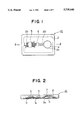
- FIGS. 1 and 2 are schematic diagrams showing a thin IC card according to an embodiment of this invention.
- FIG. 1 is a plan view of the IC card
- FIG. 2 is an enlarged sectional view taken along the line 2--2 of FIG. 1.
- the components which are the same as or equivalent to those of the conventional examples are referred to by the same reference numerals, and a description of such components will be omitted.
- the IC card 10 has obverse and reverse main surfaces. Mounted at one of these main surfaces (hereinafter “the mounting surface") on the circuit board 2 are an IC package 3, which serves as the functional part, and another part 5, with a circuit pattern 2b being formed at least at the mounting surface on the circuit board 2.
- the circuit board 2 When a circuit pattern is also formed on that circuit board 2 where no IC package is mounted (hereinafter “the reverse surface"), the circuit patterns on the obverse and reverse surfaces are connected to each other through through-holes (not shown) or the like. Further, the circuit board 2 has a through-hole portion 2a formed in correspondence with the configuration of the battery 4. This through-hole portion is a peripheral edge (the inlet) of a lodging section 8 for receiving the battery 4. Formed on a part of the periphery of the through-hole portion 2a are a pair of electrodes 20 for battery connection.
- the IC package 3 and the other part 5 are integrally formed with the circuit board 2, which is embedded in a molding-resin 7 by injection molding using a mold as shown in FIGS. 5 and 6.
- the battery lodging section 8 the peripheral edge of which includes the through-hole portion 2a, is formed by a protrusion 101a or 102a provided inside the mold.
- the lodging section 8 has a configuration corresponding to that of the battery 4 lodged therein and its depth is such that the exposed surface of the battery 4 when lodged is substantially flush with the reverse surface of the circuit board 2.
- the reverse side of the circuit board 2 is covered with a decorative sheet 6 of plastic or paper having a design indicating the kind of card, thereby completing the IC card 10.
- Liquid-crystal polymers are one example of the molding resin used.
- FIGS. 3, 4A, and 4B show a first embodiment of the structure for the electrical connection between the circuit board and the battery of the IC card of this invention, shown in FIGS. 1 and 2.
- FIG. 5 is a sectional view showing an example of the mold for resin molding used in the production of the IC card of this embodiment.
- FIG. 3 is a sectional view showing the IC card 10.
- the circuit board 2 having the functional part mounted thereon and the through-hole portion formed therein, has been embedded in the molding-resin section 7, and the battery 4 has not been lodged in the lodging section 8 yet.
- a decorative-sheet fitting section 9 for providing the decorative sheet 6 is formed on the reverse side of the molding-resin section 7, in which the circuit board 2 is embedded.
- the depth of the decorative-sheet fitting section 9 is substantially the same as the thickness of the decorative sheet 6 so that the exposed surface of the decorative sheet 6 when fitted is flush with the molding-resin section 7.
- FIGS. 4A and 4B exclusively show the circuit board 2 of the IC card shown in FIG. 3.
- FIG. 4A is a plan view seen from the side of the molding-resin section 7.
- FIG. 4B is a sectional view taken along the line 4B--4B of FIG. 4A.
- the right-hand side of FIG. 4B corresponds to the upper side of the IC card shown in FIG. 3.
- formed on a part of the periphery of the through-hole section 2a is a recess 2c for soldering or the like to electrically and mechanically connect the battery 4 to the battery-connection electrodes 20 on the circuit board 2. As shown in FIG.
- the recess 2c is formed on the side of the molding-resin section 7 when the above-described injection molding is conducted.
- the battery-connection electrodes 20 are exposed inside the recess 2c, and are connected to the circuit pattern 2b on the circuit board 2.
- the battery-connection terminals 40 are connected to the battery-connection electrodes 20 by solder 41, which is a conductive material.
- the battery-connection electrodes 20 and the battery-connection terminals 40 are generally provided one pair each.
- FIG. 5 shows an example of the mold for producing the IC card of this embodiment.
- the mold is composed of upper and lower mold sections 100 and 101. Formed on the lower mold section 101 are the protrusion 101a for forming the battery lodging section 8 and a protrusion 101b for deforming a part of the circuit board 2 into the recess 2c. These mold sections are shown only schematically, and the means for securing the circuit board 2 inside the mold and the injection outlet for the resin are omitted.
- the circuit board 2 When the functional part has been mounted on the circuit board 2 and the through-hole portion 2a has been formed therein, the circuit board 2 is put in the mold to undergo injection molding. At this time, the protrusion 101a of the lower mold section 101 is fitted into the through-hole portion 2a and, in this condition, the circuit board 2 is secured inside the mold. Thus, when injection molding is completed, the lodging section 8, whose peripheral edge includes the through-hole portion 2a of the circuit board 2, has been formed in the molding-resin section 7.
- the low, dike-like protrusion 101b adjacent to the protrusion 101a of the lower mold section 101, causes a part of the periphery of the through-hole portion 2a of the circuit board 2 to be deformed into the recess 2c, which is situated where the battery-connection electrodes 20 are located.
- the configuration of the lodging section 8 and the recess 2c can be easily changed by changing the configuration of the protrusions 101a and 101b of the lower mold section 101.
- the battery 4 is lodged in the lodging section 8 of the IC card 10 formed as an integral unit.
- the battery-connection terminals 40 extending from the battery 4 are electrically and mechanically connected to the battery-connection electrodes 20 by the solder 41 shown in FIG. 10 or the like, thereby securing the battery 4 inside the lodging section 8.
- the recess 2c must be deep enough to cover the height of the joint between the electrodes and the terminals. In practice, the recess must have a depth of approximately 0.3 mm. Molding was experimentally performed using a polyimide-film printed circuit board having a thickness of 0.2 mm as the circuit board 2. By deforming the circuit board itself, a battery-connection recess having a desired depth could be easily formed.
- the circuit board 2 When the circuit board 2 is hard to deform, it is expedient to provide a slit 2d (see FIGS. 4A and 4B) on either side of that section of the circuit board 2 where the recess 2c is to be formed.
- the decorative sheet 6, which is to be attached to the reverse side of the circuit board 2 may be omitted. In that case, there is no need to form the decorative-sheet fitting section 9 on the molding-resin section 7 when conducting resin molding.
- FIGS. 7 and 8 show a second embodiment of the structure of this invention for connecting the circuit board and the battery of the IC card to each other.
- FIG. 6 is a sectional view showing an example of the mold used in resin molding in the production of an IC card according to this embodiment.
- FIG. 7 is a sectional view showing the IC card 10 in a condition prior to lodging the battery 4 in the lodging section 8.
- FIGS. 8A and 8B exclusively show the circuit board 2 of the IC card of FIG. 7.
- FIG. 8A is a plan view of the circuit board as seen from the reverse side.
- FIG. 8B is a sectional view taken along the line 8B--8B of FIG. 8A.
- the right-hand side of FIG. 8B corresponds to the upper side of the IC card shown in FIG. 7, which is a sectional view taken along the line 8B--8B of FIG. 8A.
- a pair of cutouts 2e for battery connection are located on a part of the periphery of the through-hole portion 2a of the circuit board 2.
- a pair of flat battery-connection electrodes 20 consisting of copper foils are provided on the mounting side of the circuit board 2, covering the bottom sections of the cutouts 2e.
- the battery-connection electrodes 20 are connected to the circuit pattern 2b (see FIG. 1) on the mounting surface of the circuit board 2.
- the battery 4 shown in FIGS. 9 and 10 is lodged in the lodging section 8, and the battery-connection terminals 40 are connected to the battery-connection electrodes 20 by solder 41, a conductive material.
- FIG. 6 shows an example of the mold used in the production of the IC card of this embodiment. It is composed of upper and lower mold sections 100 and 102. Provided on the lower mold section 102 are a protrusion 102a for forming the battery lodging section 8 and a pair of protrusions 102b which engage the cutouts 2e of the circuit board 2 when the IC card is formed as an integral unit by injection molding.
- the protrusions 102b prevent intrusion of molding resin into the cutouts 2e during injection molding, thereby forming recesses for electrically connecting the circuit board 2 to the battery 4.
- the electrodes 20 are exposed on the bottom surfaces of the recesses.
- the circuit board 2 When the functional part has been mounted on the circuit board 2 and the through-hole portion 2a and the cutouts 2e have been formed therein, the circuit board 2 is put in the mold to undergo molding. At this time, the protrusion 102a of the lower mold section 102 is fitted into the through-hole portion 2a of the circuit board 2, and the protrusions 102b are fitted into the cutouts 2e and, in this condition, the circuit board 2 is secured within the mold.
- the lodging section 8 whose periphery includes the through-hole portion 2a of the circuit board 2, has been formed in the molding-resin section 7.
- the cutouts 2e remain as recesses, on the bottom surfaces of which the battery-connection electrodes 20 are exposed.
- FIG. 9 is a side view of a coin-shaped battery 4.
- the lower side of the battery 4 is the anode.
- Extending from both electrodes of the battery 4 are the battery-connection terminals 40, the ends of which are connected to the electrodes 20 of the cutouts 2e of the circuit board 2.
- FIG. 10 is a sectional view showing the connected state.
- the battery 4 is lodged in the lodging section 8, and the ends of the battery-connection terminals 40 are connected to the battery-connection electrodes 20, the connection being effected inside the cutouts 2e by means of solder 41.
- the battery connecting portions and the battery do not protrude beyond the reverse surface of the circuit board 2, so that the card surface exhibits no surface irregularities.
- the decorative sheet 6 is attached to the reverse side of the circuit board 2 as needed.
- the battery-connection electrodes 20 may be flat, as shown in FIG. 7.
- the circuit board 2 is as thin as 0.2 mm, whereas in many cases the cutouts 2e must be 0.3 mm deep or more in order to accommodate the electrode-connecting sections including the battery-connection electrodes 20, the terminals 40 and the solder 41.
- FIGS. 11 and 12 show a third embodiment of the structure of this invention for electrically connecting the circuit board and the battery of the IC card to each other.
- FIG. 11 is a sectional view showing the IC card 10 prior to lodging the battery in the lodging section 8.
- FIG. 12 is a plan view, as seen from the reverse side, showing the circuit board of the IC card of FIG. 11 exclusively. In FIG. 12, the circuit board 12 is shown prior to injection molding.
- a part of the circuit board 2 is formed as two projections 2f and 2g, which extend from the periphery of the through-hole section 2a toward the center thereof.
- the anode of the battery may be on the upper or lower side of the battery.
- the configuration of the lodging section can be changed in accordance with the configuration of the battery by changing the configuration of the protrusion of the mold accordingly. Further, by changing the configuration of the protrusion of the mold, it is possible to provide the lodging section with separate recesses into which the battery-connection electrodes are to be fitted.
- FIG. 13 is an enlarged sectional view of the lodging section 8 in which the battery 4 is accommodated.
- the gap between the lodging section 8 and the battery 4 is filled with the expandable resin 90.
- the battery 4 is embedded in the resin 90, which forms a surface flush with the reverse surface of the circuit board 2.
- the decorative sheet 6 is disposed on the reverse side of the circuit board 2. This process of embedding the battery 4 is executed on an IC card 10 as shown in FIG. 14, in which the lodging section 8 has been formed by injection molding.
- unexpanded expandable resin 90 is poured in the lodging section 8 with its opening facing upward. Then, the battery 4 is put in the lodging section 8 and electrically connected to the battery-connection electrodes (not shown) of the circuit board in accordance, for example, with one of the above-described embodiments.
- unexpanded expandable resin 90 is also poured over the battery 4 and, as shown in FIG. 15C, the entire IC card is held between upper and lower dies 103 and 104. In this condition, the resin 90 is allowed to expand and cure.
- 15D shows the resin 90 expanded and cured while the IC card is held between the dies.
- the volume of the expandable resin 90, poured both over and under the battery 4, increases to fill the gap around the battery 4, and cures in this condition.
- the dies cause the surface under which the battery 4 is embedded to become flat and flush with the reverse surface of the circuit board.
- the resin 90 When the resin 90 is allowed to expand inside the lodging section 8 of the IC card with the battery 4 lodged therein, not only the lodging section 8 but also the recess 2c or the cutouts 2e are filled with resin 90, so that the resin 90 also protects the connecting section between the battery and the circuit board.
- a three-component-type low-temperature-curing epoxy resin was used as the expandable resin 90, which was composed of: a chief component consisting of an inorganic-powder filler material, a curing agent, and a blowing agent.
- this resin becomes a closed-cell foam body having a void volume of 20 to 50%.
- An amount of unexpanded expandable resin 90 corresponding to 60% of the calculated voids was applied to the spaces above and below the battery 4, and the entire card was held between lubricated dies. The resin was then allowed to expand and cure at 50° C. After the resin 90 had expanded and filled up the space around the battery 4, the expansion of the resin was restricted by the fastening pressure of the dies. In this condition, the expansion was completed along with the curing, and the configuration of the resin was fixed.
- the battery can be embedded in the lodging section. Further, the surface of the lodging section under which the battery is embedded can be made flat and flush with the reverse surface of the circuit board, thus realizing an IC card of a completely solid type, the surface of which has even fewer irregularities. Further, since the battery 4 is secured inside the body of the IC card, that is, made integral with the IC card, the electrical-connection portion between the battery and the circuit board has a very high level of reliability with respect to vibrations of the IC card and other external forces.
- the battery 4 is covered with the expandable resin 90, no stress due to contraction during curing of the resin is applied to the battery as in the case where the lodging section is filled with thermosetting resin or the like.
- the battery is covered with closed-cell foam resin in such a way as to leave no surface of it exposed, the IC card is good for use even under unfavorable environmental conditions.
- thermosetting-type expandable resin was used, the same effect can be obtained by using other types of expandable resins.
- a resin which is resistant to elastic deformation after it has expanded and cured it is desirable to use a resin which is resistant to elastic deformation after it has expanded and cured.
- a through-hole portion at the edge of the battery lodging section is formed in the circuit board, on which the functional part is mounted, and this circuit board is embedded in the molding-resin section in such a way that its reverse surface is exposed.
- the battery lodging section is formed in the molding-resin section in correspondence with the through-hole portion of the circuit board, and the electrical connection of the circuit board to the battery is effected in the recess or cutouts formed on the circuit board, thereby realizing a thin IC card having a flat surface with no irregularities.
- the battery Since the battery is accommodated in the lodging section after the formation of the molding-resin section, the battery is free from damage from the heat generated during resin molding.
- the battery lodging section is formed by resin molding, it can be formed into a desired configuration in accordance with the configuration of the battery.
- the surface of the card can be made even flatter. Also, the reliability of the electrical connection between the battery and the circuit board is improved.
Abstract
A method of producing a thin IC card having a built-in battery includes forming a through-hole including an edge in a circuit board having obverse and reverse main surfaces, a circuit pattern being present on a first of the main surfaces of the circuit board; mounting a functional part on the first of the main surfaces of the circuit board; molding said circuit board and said functional part in a resin with a second main surface of said circuit exposed and forming a battery lodging section in the resin molding defined by the through-hole; and mounting a battery in said battery lodging section and electrically connecting the circuit pattern to the battery.
Description
This disclosure is a division of patent application Ser. No. 07/994,957, filed Dec. 22, 1992 now U.S. Pat. No. 5,677,568.
1. Field of the Invention
This invention relates to a thin IC card having a built-in battery and, in particular, to a thin IC card having a functional part and battery completely embedded in resin.
2. Description of the Related Art
FIG. 16 is a sectional view of a conventional thin IC card (hereinafter "IC card"). An IC card 1 includes a circuit board 2 lodged and secured in position inside a plastic frame 11. Mounted on the circuit board 2 are: an IC package 3, serving as the functional part, a battery 4, and another part 5. Panels 60, consisting of thin metal sheets, are glued to the upper and lower surfaces of the frame 11 by an adhesive (not shown).
FIG. 17 shows a sectional view of another conventional IC card. In this IC card 1, the spaces defined between the circuit board 2, on which the battery 4 and the other part 5 are mounted, and the upper and lower panels 60, are filled with curable resin 12 by potting or the like, thereby forming a solid-type IC card. In a non-contact IC card having a built-in communication device, such as a coil, use of metal sheets as the panels is restricted. In view of this, plastic sheets have been used as the panels 60 on the surfaces of the IC card and, to enhance the strength thereof, the panels 60 have been made thick or, as in the IC card shown in FIG. 17, the gaps between the circuit board 2 and the upper and lower panels 60 have been filled with the resin 12.
A problem with the conventional IC card shown in FIG. 16 is that, as it has the gaps between the panels 60 and the circuit board 2, the panels are liable to be distorted or bent when an external force is applied to the surfaces of the card. When the IC card is formed as a non-contact card for communicating information by electromagnetic waves, the panels must be made of a non-metal material. In that case, panels of synthetic resin which are very thick are used to ensure the requisite strength, with the result that the entire IC card is rather thick.
In the case of the IC card shown in FIG. 17, the inner spaces, as mentioned above, are filled with resin to ensure the requisite strength. However, it is difficult to pour a quantity of resin in the spaces which is just enough to fill the spaces, i.e., neither too much nor too little resin. This is particularly true in the case of a card whose panels have to be made of thermoplastic resin material. In such a case, it is difficult to make the surfaces of the card flat and parallel. Further, when the resin contracts as a result of curing, a part of each of the card surfaces may be drawn inwardly. Due to the presence of the functional part inside the card, such a contraction will result in the generation of irregularities on the card surfaces. Further, there is the problem of resin leaking through the joints between the panels and the frame. Apart from this, a number of complicated processes are required to fill the inner spaces with resin, such as blending and curing. In addition, when the card is being filled with resin at a high temperature, heat is applied to the battery, thereby deteriorating the function of the battery.
This invention has been made with a view toward solving the above problems. It is an object of this invention to provide a thin IC card with flat surfaces and a production method for the same which allow the battery to be easily mounted in the card without being damaged.
In order to achieve the above object, there is provided, in accordance with this invention, a thin IC card having a built-in battery, the IC card comprising: a circuit board having obverse and reverse main surfaces on one of which a functional part is mounted, and a through-hole portion constituting an edge around a lodging section in which the battery is lodged, a circuit pattern being formed at least on that main surface of the circuit board on which the functional part is mounted; a molding-resin section formed as a card in such a way that the circuit board and the functional part are embedded therein, exposing that main surface of the circuit board on which the functional part is not mounted, the lodging section in which the battery is lodged being formed in the molding-resin section in such a way that the through-hole portion of the circuit board constitutes an inlet of the lodging section; and battery connection means for firmly supporting the battery in the lodging section and for electrically connecting the battery to the circuit pattern on the circuit board.
In this invention the battery connection means electrically connects the circuit pattern on the circuit board to the battery through a recess or a cutout on the circuit board.
In another embodiment of this invention, the section between the battery and the lodging section is filled with an expandable resin, which forms a flat surface together with the circuit board surface.
In still another embodiment of this invention, a decorative sheet is disposed on that main surface of the circuit board on which the functional part is not mounted, the molding-resin section being formed in such a way that the circuit board, on which the functional part is mounted, and the decorative sheet are embedded in such a way that one side of the decorative sheet is exposed, with the exposed main surface of the decorative sheet and the molding-resin section forming one flat surface.
This invention also covers a method of producing such a thin IC card.
In the thin IC card of this invention, a through-hole portion constituting an inlet for the battery lodging section is formed on the circuit board, and the functional part of the circuit board is embedded in the molding-resin section. At the same time, the battery lodging section is formed through the intermediation of the through-hole portion, so that the lodging section can be formed in correspondence with the configuration of the battery.
Further, a recess section is provided in the peripheral edge around the through-hole portion of the circuit board, and the electrical connection between the circuit pattern of the circuit board and the battery is effected through this recess section, thereby making the card surface flat, including the battery lodging section.
The battery lodging section is filled with an expandable resin, whereby the battery is more firmly fixed inside the lodging section and the card surface can be kept flatter, thereby realizing a highly reliable battery lodging section.
Further, in the thin IC card production method of this invention, the battery is mounted on the card and electrically connected to the circuit board after the integral molding of the card, so that the battery can be easily mounted and is free from damage by heat during the integral molding.
FIG. 1 is a schematic plan view of a thin IC card according an embodiment of this invention;
FIG. 2 is an enlarged sectional view taken along the line 2--2 of FIG. 1;
FIG. 3 is a sectional view of a thin IC card according to this invention, showing an embodiment of the structure for connecting the circuit board to the battery;
FIG. 4A is a plan view of the circuit board shown in FIG. 3, and FIG. 4B is a sectional view taken along the line 4B--4B of FIG. 4A;
FIG. 5 is sectional view of a mold for producing the thin IC card shown in FIG. 3;
FIG. 6 is sectional view of a mold for producing the thin IC card shown in FIG. 7;
FIG. 7 is a sectional view taken along the line 7--7 of FIG. 8A, of a thin IC card according to this invention, showing another embodiment of the structure for connecting the circuit board to the battery;
FIG. 8A is a plan view of the circuit board shown in FIG. 7, and FIG. 8B is a sectional view taken along the line 8B--8B of FIG. 8A;
FIG. 9 is a side view of a battery used in this invention;
FIG. 10 is a partial sectional view showing how the battery is lodged in the thin IC card shown in FIG. 7;
FIG. 11 is a sectional view of a thin IC card according to this invention, showing still another embodiment of the structure for connecting the circuit board to the battery;
FIG. 12 is a plan view of the circuit board shown in FIG. 11 prior to resin molding;
FIG. 13 is a partial sectional view of a thin IC card according to another embodiment of this invention, showing the battery lodging section;
FIG. 14 is a sectional view of the thin IC card shown in FIG. 13 prior to embedding its battery in expandable resin;
FIGS. 15A through 15D are sectional views showing the procedures for embedding the battery of the thin IC card of FIG. 13 in expandable resin;
FIG. 16 is a sectional view showing a conventional thin IC card; and
FIG. 17 is a sectional view showing another conventional thin IC card.
Embodiments of this invention will now be described with reference to the accompanying drawings.
FIGS. 1 and 2 are schematic diagrams showing a thin IC card according to an embodiment of this invention. FIG. 1 is a plan view of the IC card, and FIG. 2 is an enlarged sectional view taken along the line 2--2 of FIG. 1. The components which are the same as or equivalent to those of the conventional examples are referred to by the same reference numerals, and a description of such components will be omitted. The IC card 10 has obverse and reverse main surfaces. Mounted at one of these main surfaces (hereinafter "the mounting surface") on the circuit board 2 are an IC package 3, which serves as the functional part, and another part 5, with a circuit pattern 2b being formed at least at the mounting surface on the circuit board 2. When a circuit pattern is also formed on that circuit board 2 where no IC package is mounted (hereinafter "the reverse surface"), the circuit patterns on the obverse and reverse surfaces are connected to each other through through-holes (not shown) or the like. Further, the circuit board 2 has a through-hole portion 2a formed in correspondence with the configuration of the battery 4. This through-hole portion is a peripheral edge (the inlet) of a lodging section 8 for receiving the battery 4. Formed on a part of the periphery of the through-hole portion 2a are a pair of electrodes 20 for battery connection.
The IC package 3 and the other part 5 are integrally formed with the circuit board 2, which is embedded in a molding-resin 7 by injection molding using a mold as shown in FIGS. 5 and 6. In this injection molding, the battery lodging section 8, the peripheral edge of which includes the through-hole portion 2a, is formed by a protrusion 101a or 102a provided inside the mold. The lodging section 8 has a configuration corresponding to that of the battery 4 lodged therein and its depth is such that the exposed surface of the battery 4 when lodged is substantially flush with the reverse surface of the circuit board 2. When the battery 4 has been lodged in the lodging section 8 and battery-connection terminals 40 of the battery 4 have been connected to the battery-connection electrodes 20 provided on the circuit board 2 (see FIGS. 4A, 4B, 9 and 10), the reverse side of the circuit board 2 is covered with a decorative sheet 6 of plastic or paper having a design indicating the kind of card, thereby completing the IC card 10. Liquid-crystal polymers are one example of the molding resin used.
FIGS. 3, 4A, and 4B show a first embodiment of the structure for the electrical connection between the circuit board and the battery of the IC card of this invention, shown in FIGS. 1 and 2. FIG. 5 is a sectional view showing an example of the mold for resin molding used in the production of the IC card of this embodiment.
FIG. 3 is a sectional view showing the IC card 10. In this drawing, the circuit board 2, having the functional part mounted thereon and the through-hole portion formed therein, has been embedded in the molding-resin section 7, and the battery 4 has not been lodged in the lodging section 8 yet. Referring to FIG. 3, a decorative-sheet fitting section 9 for providing the decorative sheet 6 is formed on the reverse side of the molding-resin section 7, in which the circuit board 2 is embedded. The depth of the decorative-sheet fitting section 9 is substantially the same as the thickness of the decorative sheet 6 so that the exposed surface of the decorative sheet 6 when fitted is flush with the molding-resin section 7.
FIGS. 4A and 4B exclusively show the circuit board 2 of the IC card shown in FIG. 3. FIG. 4A is a plan view seen from the side of the molding-resin section 7. FIG. 4B is a sectional view taken along the line 4B--4B of FIG. 4A. The right-hand side of FIG. 4B corresponds to the upper side of the IC card shown in FIG. 3. Referring to FIG. 4A, formed on a part of the periphery of the through-hole section 2a is a recess 2c for soldering or the like to electrically and mechanically connect the battery 4 to the battery-connection electrodes 20 on the circuit board 2. As shown in FIG. 3, the recess 2c is formed on the side of the molding-resin section 7 when the above-described injection molding is conducted. As shown in FIG. 4B, the battery-connection electrodes 20 are exposed inside the recess 2c, and are connected to the circuit pattern 2b on the circuit board 2. As shown in FIGS. 9 and 10, the battery-connection terminals 40 are connected to the battery-connection electrodes 20 by solder 41, which is a conductive material. The battery-connection electrodes 20 and the battery-connection terminals 40 are generally provided one pair each.
FIG. 5 shows an example of the mold for producing the IC card of this embodiment. The mold is composed of upper and lower mold sections 100 and 101. Formed on the lower mold section 101 are the protrusion 101a for forming the battery lodging section 8 and a protrusion 101b for deforming a part of the circuit board 2 into the recess 2c. These mold sections are shown only schematically, and the means for securing the circuit board 2 inside the mold and the injection outlet for the resin are omitted.
When the functional part has been mounted on the circuit board 2 and the through-hole portion 2a has been formed therein, the circuit board 2 is put in the mold to undergo injection molding. At this time, the protrusion 101a of the lower mold section 101 is fitted into the through-hole portion 2a and, in this condition, the circuit board 2 is secured inside the mold. Thus, when injection molding is completed, the lodging section 8, whose peripheral edge includes the through-hole portion 2a of the circuit board 2, has been formed in the molding-resin section 7. At the same time, the low, dike-like protrusion 101b, adjacent to the protrusion 101a of the lower mold section 101, causes a part of the periphery of the through-hole portion 2a of the circuit board 2 to be deformed into the recess 2c, which is situated where the battery-connection electrodes 20 are located. The configuration of the lodging section 8 and the recess 2c can be easily changed by changing the configuration of the protrusions 101a and 101b of the lower mold section 101.
The battery 4 is lodged in the lodging section 8 of the IC card 10 formed as an integral unit. Next, the battery-connection terminals 40, extending from the battery 4, are electrically and mechanically connected to the battery-connection electrodes 20 by the solder 41 shown in FIG. 10 or the like, thereby securing the battery 4 inside the lodging section 8. The recess 2c must be deep enough to cover the height of the joint between the electrodes and the terminals. In practice, the recess must have a depth of approximately 0.3 mm. Molding was experimentally performed using a polyimide-film printed circuit board having a thickness of 0.2 mm as the circuit board 2. By deforming the circuit board itself, a battery-connection recess having a desired depth could be easily formed.
When the circuit board 2 is hard to deform, it is expedient to provide a slit 2d (see FIGS. 4A and 4B) on either side of that section of the circuit board 2 where the recess 2c is to be formed. The decorative sheet 6, which is to be attached to the reverse side of the circuit board 2, may be omitted. In that case, there is no need to form the decorative-sheet fitting section 9 on the molding-resin section 7 when conducting resin molding.
FIGS. 7 and 8 show a second embodiment of the structure of this invention for connecting the circuit board and the battery of the IC card to each other. FIG. 6 is a sectional view showing an example of the mold used in resin molding in the production of an IC card according to this embodiment. FIG. 7 is a sectional view showing the IC card 10 in a condition prior to lodging the battery 4 in the lodging section 8. FIGS. 8A and 8B exclusively show the circuit board 2 of the IC card of FIG. 7. FIG. 8A is a plan view of the circuit board as seen from the reverse side. FIG. 8B is a sectional view taken along the line 8B--8B of FIG. 8A. The right-hand side of FIG. 8B corresponds to the upper side of the IC card shown in FIG. 7, which is a sectional view taken along the line 8B--8B of FIG. 8A.
In this embodiment, a pair of cutouts 2e for battery connection are located on a part of the periphery of the through-hole portion 2a of the circuit board 2. A pair of flat battery-connection electrodes 20 consisting of copper foils are provided on the mounting side of the circuit board 2, covering the bottom sections of the cutouts 2e. The battery-connection electrodes 20 are connected to the circuit pattern 2b (see FIG. 1) on the mounting surface of the circuit board 2. The battery 4 shown in FIGS. 9 and 10 is lodged in the lodging section 8, and the battery-connection terminals 40 are connected to the battery-connection electrodes 20 by solder 41, a conductive material.
FIG. 6 shows an example of the mold used in the production of the IC card of this embodiment. It is composed of upper and lower mold sections 100 and 102. Provided on the lower mold section 102 are a protrusion 102a for forming the battery lodging section 8 and a pair of protrusions 102b which engage the cutouts 2e of the circuit board 2 when the IC card is formed as an integral unit by injection molding. The protrusions 102b prevent intrusion of molding resin into the cutouts 2e during injection molding, thereby forming recesses for electrically connecting the circuit board 2 to the battery 4. The electrodes 20 are exposed on the bottom surfaces of the recesses.
When the functional part has been mounted on the circuit board 2 and the through-hole portion 2a and the cutouts 2e have been formed therein, the circuit board 2 is put in the mold to undergo molding. At this time, the protrusion 102a of the lower mold section 102 is fitted into the through-hole portion 2a of the circuit board 2, and the protrusions 102b are fitted into the cutouts 2e and, in this condition, the circuit board 2 is secured within the mold. Thus, when injection molding is completed, the lodging section 8, whose periphery includes the through-hole portion 2a of the circuit board 2, has been formed in the molding-resin section 7. At the same time, due to the protrusions 102b, adjacent to the protrusion 102a of the lower mold section 102 and having a size corresponding to the cutouts 2e, the cutouts 2e remain as recesses, on the bottom surfaces of which the battery-connection electrodes 20 are exposed.
The battery 4 is lodged in the lodging section 8 of the IC card 10 formed as an integral unit. FIG. 9 is a side view of a coin-shaped battery 4. In the drawing, the lower side of the battery 4 is the anode. Extending from both electrodes of the battery 4 are the battery-connection terminals 40, the ends of which are connected to the electrodes 20 of the cutouts 2e of the circuit board 2. FIG. 10 is a sectional view showing the connected state. The battery 4 is lodged in the lodging section 8, and the ends of the battery-connection terminals 40 are connected to the battery-connection electrodes 20, the connection being effected inside the cutouts 2e by means of solder 41. Thus, as can be seen from FIG. 10, the battery connecting portions and the battery do not protrude beyond the reverse surface of the circuit board 2, so that the card surface exhibits no surface irregularities. Then, the decorative sheet 6 is attached to the reverse side of the circuit board 2 as needed.
When the circuit board 2 has a sufficient thickness, the battery-connection electrodes 20 may be flat, as shown in FIG. 7. Generally speaking, however, the circuit board 2 is as thin as 0.2 mm, whereas in many cases the cutouts 2e must be 0.3 mm deep or more in order to accommodate the electrode-connecting sections including the battery-connection electrodes 20, the terminals 40 and the solder 41. In view of this, it is expedient to impart a dome-like shape to the battery-connection electrodes 20, as shown in FIG. 8B, making the depth of the battery-connection recesses, defined by the cutouts 2e, approximately 0.4 mm. This can be easily realized, for example, by increasing the height of the protrusions 102b of the lower mold section 102 shown in FIG. 6.
FIGS. 11 and 12 show a third embodiment of the structure of this invention for electrically connecting the circuit board and the battery of the IC card to each other. FIG. 11 is a sectional view showing the IC card 10 prior to lodging the battery in the lodging section 8. FIG. 12 is a plan view, as seen from the reverse side, showing the circuit board of the IC card of FIG. 11 exclusively. In FIG. 12, the circuit board 12 is shown prior to injection molding.
In this embodiment, a part of the circuit board 2 is formed as two projections 2f and 2g, which extend from the periphery of the through-hole section 2a toward the center thereof. Formed on the surfaces of the projections 2f and 2g facing the battery (not shown) are battery-connection electrodes 20 extending from the reverse surface of the circuit board. When the circuit board 2 is put in the mold and injection molding is performed, the projections 2f and 2g are pressed and bent by the protrusion formed on the lower mold section and deformed along the inner surface of the lodging section 8, as shown in FIG. 11. This enables the battery-connection electrodes 20, formed on the projections 2f and 2g, to come into contact with the electrodes of the battery lodged in the lodging section 8. When the battery has been lodged in the lodging section, the battery and the battery-connection electrodes 20 are electrically connected to each other. In this way, it is possible to lodge the battery without allowing it to protrude beyond the reverse surface of the circuit board 2.
The anode of the battery may be on the upper or lower side of the battery. The configuration of the lodging section can be changed in accordance with the configuration of the battery by changing the configuration of the protrusion of the mold accordingly. Further, by changing the configuration of the protrusion of the mold, it is possible to provide the lodging section with separate recesses into which the battery-connection electrodes are to be fitted.
Further, in accordance with this invention, it is also possible, as shown in FIG. 13, to put unexpanded expandable resin 90 in the lodging section 8 accommodating the battery 4. When expanded, this resin fills the gap between the lodging section 8 and the battery 4. This will be described with reference to FIGS. 13 to 15.
FIG. 13 is an enlarged sectional view of the lodging section 8 in which the battery 4 is accommodated. The gap between the lodging section 8 and the battery 4 is filled with the expandable resin 90. Thus, the battery 4 is embedded in the resin 90, which forms a surface flush with the reverse surface of the circuit board 2. Further, the decorative sheet 6 is disposed on the reverse side of the circuit board 2. This process of embedding the battery 4 is executed on an IC card 10 as shown in FIG. 14, in which the lodging section 8 has been formed by injection molding.
The battery embedding procedures will be described with reference to FIGS. 15A to 15D. First, as shown in FIG. 15A, unexpanded expandable resin 90 is poured in the lodging section 8 with its opening facing upward. Then, the battery 4 is put in the lodging section 8 and electrically connected to the battery-connection electrodes (not shown) of the circuit board in accordance, for example, with one of the above-described embodiments. Next, as shown in FIG. 15B, unexpanded expandable resin 90 is also poured over the battery 4 and, as shown in FIG. 15C, the entire IC card is held between upper and lower dies 103 and 104. In this condition, the resin 90 is allowed to expand and cure. FIG. 15D shows the resin 90 expanded and cured while the IC card is held between the dies. The volume of the expandable resin 90, poured both over and under the battery 4, increases to fill the gap around the battery 4, and cures in this condition. The dies cause the surface under which the battery 4 is embedded to become flat and flush with the reverse surface of the circuit board.
When the resin 90 is allowed to expand inside the lodging section 8 of the IC card with the battery 4 lodged therein, not only the lodging section 8 but also the recess 2c or the cutouts 2e are filled with resin 90, so that the resin 90 also protects the connecting section between the battery and the circuit board.
In this embodiment, a three-component-type low-temperature-curing epoxy resin was used as the expandable resin 90, which was composed of: a chief component consisting of an inorganic-powder filler material, a curing agent, and a blowing agent. When allowed to expand, this resin becomes a closed-cell foam body having a void volume of 20 to 50%. An amount of unexpanded expandable resin 90 corresponding to 60% of the calculated voids was applied to the spaces above and below the battery 4, and the entire card was held between lubricated dies. The resin was then allowed to expand and cure at 50° C. After the resin 90 had expanded and filled up the space around the battery 4, the expansion of the resin was restricted by the fastening pressure of the dies. In this condition, the expansion was completed along with the curing, and the configuration of the resin was fixed.
In this way, the battery can be embedded in the lodging section. Further, the surface of the lodging section under which the battery is embedded can be made flat and flush with the reverse surface of the circuit board, thus realizing an IC card of a completely solid type, the surface of which has even fewer irregularities. Further, since the battery 4 is secured inside the body of the IC card, that is, made integral with the IC card, the electrical-connection portion between the battery and the circuit board has a very high level of reliability with respect to vibrations of the IC card and other external forces.
Further, since the battery 4 is covered with the expandable resin 90, no stress due to contraction during curing of the resin is applied to the battery as in the case where the lodging section is filled with thermosetting resin or the like. In addition, since the battery is covered with closed-cell foam resin in such a way as to leave no surface of it exposed, the IC card is good for use even under unfavorable environmental conditions.
Although in the above embodiment a thermosetting-type expandable resin was used, the same effect can be obtained by using other types of expandable resins. However, in view of the fact that the IC card is to exhibit a flat surface with no irregularities, it is desirable to use a resin which is resistant to elastic deformation after it has expanded and cured.
As described above, in accordance with this invention, a through-hole portion at the edge of the battery lodging section is formed in the circuit board, on which the functional part is mounted, and this circuit board is embedded in the molding-resin section in such a way that its reverse surface is exposed. The battery lodging section is formed in the molding-resin section in correspondence with the through-hole portion of the circuit board, and the electrical connection of the circuit board to the battery is effected in the recess or cutouts formed on the circuit board, thereby realizing a thin IC card having a flat surface with no irregularities.
Since the battery is accommodated in the lodging section after the formation of the molding-resin section, the battery is free from damage from the heat generated during resin molding.
Further, since the battery lodging section is formed by resin molding, it can be formed into a desired configuration in accordance with the configuration of the battery.
In addition, by filling the gap between the battery and the lodging section with expandable resin, the surface of the card can be made even flatter. Also, the reliability of the electrical connection between the battery and the circuit board is improved.
Claims (8)
1. A method of producing a thin IC card having a built-in battery comprising:
forming a through-hole including an edge, in a circuit board, the circuit board having first and second main surfaces, a circuit pattern being present on the first main surface;
mounting a functional part on the first main surface;
forming a card-shaped section including:
inserting the circuit board with the functional part into a mold, the mold including a first protrusion extending through the through-hole in the circuit board; and
injecting a resin into the mold to form the card-shaped section including a battery lodging section at the through hole, the resin covering the first main surface but not the second main surface; and
mounting a battery in the battery lodging section and electrically connecting the circuit pattern to the battery.
2. The method of producing a thin IC card according to claim 1 comprising:
in forming the card-shaped section, forming a recess in the card-shaped section at the second main surface, adjacent to the through-hole and to the circuit board;
forming at least a pair of battery-connection electrodes in the recess; and
in mounting the battery, connecting the battery-connection electrodes in the recess to respective connection terminals of the battery.
3. The method of producing a thin IC card according to claim 2 wherein forming the recess comprises forming at least one slit in the circuit board adjacent to the through-hole.
4. The method of producing a thin IC card according to claim 1 including:
forming in the circuit board at least a pair of cutouts extending from the first main surface to the second main surface at the edge of the through-hole; and
connecting at least a pair of battery-connection electrodes to the circuit pattern on the first main surface of the circuit board, the battery connection electrodes covering the cutouts, wherein
forming the card-shaped section includes inserting the circuit board including the cutouts and the battery-connection electrodes into the mold, the mold including at least a pair of second protrusions, the second protrusions preventing intrusion of the resin into the cutouts, and
mounting the battery includes inserting a pair of connection terminals of the battery into the cutouts from the second main surface and connecting the connection terminals to the battery-connection electrodes covering the cutouts.
5. The method of producing a IC card according to claim 4 wherein the battery-connection electrodes covering the cutouts are dome-shaped electrodes indented toward the card-shaped section.
6. The method of producing a thin IC card according to claim 1 including:
forming at least a pair of projections of the circuit board extending toward the center of the through-hole; and
attaching at least a pair of battery-connection electrodes to the projections, wherein forming the card-shaped section includes inserting the circuit board into the mold, the first protrusion bending the projections away from the through-hole to form the battery lodging section.
7. The method of producing a thin IC card according to claim 1 comprising, after forming the card-shaped section, placing an unexpanded expandable resin in the battery lodging section and, after mounting the battery, while holding the card between dies, expanding the expandable resin to fill the battery lodging section and to form a flat surface flush with the second surface.
8. The method of producing a thin IC card according to claim 1 including, in forming the card-shaped section, forming a decorative-sheet fitting section having a depth equal to a thickness of a decorative sheet in the card-shaped section, and fitting the decorative sheet into the decorative-sheet fitting section.
Priority Applications (1)
| Application Number | Priority Date | Filing Date | Title |
|---|---|---|---|
| US08/716,540 US5735040A (en) | 1991-12-26 | 1996-09-19 | Method of making IC card |
Applications Claiming Priority (4)
| Application Number | Priority Date | Filing Date | Title |
|---|---|---|---|
| JP3-345327 | 1991-12-26 | ||
| JP3345327A JPH05169885A (en) | 1991-12-26 | 1991-12-26 | Thin ic card |
| US07/994,957 US5677568A (en) | 1991-12-26 | 1992-12-22 | Thin IC card |
| US08/716,540 US5735040A (en) | 1991-12-26 | 1996-09-19 | Method of making IC card |
Related Parent Applications (1)
| Application Number | Title | Priority Date | Filing Date |
|---|---|---|---|
| US07/994,957 Division US5677568A (en) | 1991-12-26 | 1992-12-22 | Thin IC card |
Publications (1)
| Publication Number | Publication Date |
|---|---|
| US5735040A true US5735040A (en) | 1998-04-07 |
Family
ID=18375842
Family Applications (2)
| Application Number | Title | Priority Date | Filing Date |
|---|---|---|---|
| US07/994,957 Expired - Fee Related US5677568A (en) | 1991-12-26 | 1992-12-22 | Thin IC card |
| US08/716,540 Expired - Fee Related US5735040A (en) | 1991-12-26 | 1996-09-19 | Method of making IC card |
Family Applications Before (1)
| Application Number | Title | Priority Date | Filing Date |
|---|---|---|---|
| US07/994,957 Expired - Fee Related US5677568A (en) | 1991-12-26 | 1992-12-22 | Thin IC card |
Country Status (4)
| Country | Link |
|---|---|
| US (2) | US5677568A (en) |
| JP (1) | JPH05169885A (en) |
| DE (1) | DE4243654C2 (en) |
| FR (1) | FR2687817B1 (en) |
Cited By (50)
| Publication number | Priority date | Publication date | Assignee | Title |
|---|---|---|---|---|
| US6031242A (en) * | 1998-01-23 | 2000-02-29 | Zevatech, Inc. | Semiconductor die in-flight registration and orientation method and apparatus |
| US6077022A (en) * | 1997-02-18 | 2000-06-20 | Zevatech Trading Ag | Placement machine and a method to control a placement machine |
| US6080354A (en) * | 1997-05-01 | 2000-06-27 | Apic Yamada Corporation | Resin molding method in which a movable cavity piece allows a direct resin feed |
| US6129040A (en) * | 1997-09-05 | 2000-10-10 | Esec Sa | Semi-conductor mounting apparatus for applying adhesive to a substrate |
| US6135339A (en) * | 1998-01-26 | 2000-10-24 | Esec Sa | Ultrasonic transducer with a flange for mounting on an ultrasonic welding device, in particular on a wire bonder |
| US6157870A (en) * | 1997-02-18 | 2000-12-05 | Zevatech Trading Ag | Apparatus supplying components to a placement machine with splice sensor |
| US6179938B1 (en) | 1997-10-30 | 2001-01-30 | Esec Sa | Method and apparatus for aligning the bonding head of a bonder, in particular a die bonder |
| US6185815B1 (en) | 1997-12-07 | 2001-02-13 | Esec Sa | Semiconductor mounting apparatus with a chip gripper travelling back and forth |
| US6250934B1 (en) | 1998-06-23 | 2001-06-26 | Intel Corporation | IC package with quick connect feature |
| US6259606B1 (en) * | 1996-04-03 | 2001-07-10 | Peter Bunert | Housing for electronic circuit implementable in an electronic card, and a method of manufacturing such a card |
| US6271801B2 (en) | 1997-05-01 | 2001-08-07 | Micron Technology, Inc. | Embedded circuits |
| US6330162B2 (en) * | 1998-03-17 | 2001-12-11 | Sanyo Electric Co., Ltd. | IC card module, manufacturing method therefor, hybrid integrated circuit module, and manufacturing method thereof |
| US6436318B1 (en) * | 2000-03-30 | 2002-08-20 | Intel Corporation | Paper substrates for use in integrated circuit packaging molding processes |
| US20020186549A1 (en) * | 2001-06-11 | 2002-12-12 | Bolken Todd O. | Alternative method used to package multi media card by transfer molding |
| US20030226899A1 (en) * | 2002-06-11 | 2003-12-11 | Lenscard U.S., Llc | Method for making a financial transaction card with embedded electronic circuitry |
| US20040004274A1 (en) * | 1997-02-25 | 2004-01-08 | Wensel Richard W. | Semiconductor die with attached heat sink and transfer mold |
| US6704204B1 (en) * | 1998-06-23 | 2004-03-09 | Intel Corporation | IC package with edge connect contacts |
| US20040183182A1 (en) * | 2002-01-23 | 2004-09-23 | Susan Swindlehurst | Apparatus incorporating small-feature-size and large-feature-size components and method for making same |
| US20040188531A1 (en) * | 2003-03-24 | 2004-09-30 | Gengel Glenn W. | RFID tags and processes for producing RFID tags |
| US20040229118A1 (en) * | 2003-05-13 | 2004-11-18 | Wensley C. Glen | Card with embedded IC and electrochemical cell |
| US20040246099A1 (en) * | 1992-08-12 | 2004-12-09 | Micron Technology, Inc. | Miniature radio frequency transceiver |
| US20050046018A1 (en) * | 1999-03-16 | 2005-03-03 | Jacobsen Jeffrey Jay | Electronic devices with small functional elements supported on a carrier |
| US20050136852A1 (en) * | 2003-12-17 | 2005-06-23 | Denso Corporation | Wireless transceiver for automotive vehicle |
| US20050153209A1 (en) * | 2003-07-29 | 2005-07-14 | Alain Vallee | Polyimide-based lithium metal battery |
| US6940022B1 (en) | 1997-12-18 | 2005-09-06 | Vlt, Inc. | Protective coating for an electronic device |
| US20050227582A1 (en) * | 2004-01-16 | 2005-10-13 | Kloos Wade M | Composite model construction and method |
| US20050250015A1 (en) * | 2003-05-13 | 2005-11-10 | Wensley C G | Polyimide matrix electrolyte and improved batteries therefrom |
| US20050270757A1 (en) * | 2001-05-31 | 2005-12-08 | Credelle Thomas L | Electronic devices with small functional elements supported on a carrier |
| US20060097849A1 (en) * | 1997-08-18 | 2006-05-11 | Dando Ross S | Wireless communication devices and methods of forming and operating the same |
| US20060109130A1 (en) * | 2004-11-22 | 2006-05-25 | Hattick John B | Radio frequency identification (RFID) tag for an item having a conductive layer included or attached |
| US20060109123A1 (en) * | 2004-11-22 | 2006-05-25 | Curt Carrender | Radio frequency identification (RFID) tag for an item having a conductive layer included or attached |
| US20060109129A1 (en) * | 2004-11-22 | 2006-05-25 | Curt Carrender | Transponder incorporated into an electronic device |
| US7106201B2 (en) * | 1997-08-20 | 2006-09-12 | Micron Technology, Inc. | Communication devices, remote intelligent communication devices, electronic communication devices, methods of forming remote intelligent communication devices and methods of forming a radio frequency identification device |
| US20060245145A1 (en) * | 2005-04-28 | 2006-11-02 | Denso Corporation | Wireless communicating apparatus and production method therefor |
| US20070069358A1 (en) * | 2005-09-26 | 2007-03-29 | International Business Machines Corporation | Gel package structural enhancement of compression system board connections |
| US20070069754A1 (en) * | 2005-09-26 | 2007-03-29 | International Business Machines Corporation | Gel package structural enhancement of compression system board connections |
| US20070069753A1 (en) * | 2005-09-26 | 2007-03-29 | International Business Machines Corporation | Gel package structural enhancement of compression system board connections |
| US20070072450A1 (en) * | 2005-09-26 | 2007-03-29 | International Business Machines Corporation | Gel package structural enhancement of compression system board connections |
| US7198870B2 (en) | 2003-05-13 | 2007-04-03 | Solicore, Inc. | Polyimide matrix electrolyte |
| WO2007134429A1 (en) * | 2006-05-18 | 2007-11-29 | Ozomax Inc. | Miniature ozone generator and use thereof for purifying water |
| US20080197533A1 (en) * | 2007-02-17 | 2008-08-21 | Paul Tsao | Payment card manufacturing technology |
| US20090038145A1 (en) * | 2002-02-13 | 2009-02-12 | Matsushita Electric Industrial Co., Ltd. | Method for manufacturing a battery pack |
| US20090059498A1 (en) * | 2007-09-03 | 2009-03-05 | Samsung Electronics Co., Ltd. | Electronic appliance and method for manufacturing the same |
| US20090286150A1 (en) * | 2004-07-22 | 2009-11-19 | Solicore, Inc. | Battery tab and packaging frame design |
| US20100055943A1 (en) * | 2008-08-29 | 2010-03-04 | Park Jeong Hyun | Circuit board for memory card, and memory card having the same |
| US20110001618A1 (en) * | 2009-07-03 | 2011-01-06 | Noriyuki Yabushita | Method for attaching a flat-shaped battery and apparatus to be attached to a rotary portion |
| US20110110063A1 (en) * | 2009-11-12 | 2011-05-12 | Roche Diagnostics Operations, Inc. | Robust Consumer Electronic Device |
| DE102010039417A1 (en) * | 2010-08-17 | 2012-02-23 | Bayerische Motoren Werke Aktiengesellschaft | Redistribution element for an energy storage module and energy storage module |
| US20130099003A1 (en) * | 2010-07-01 | 2013-04-25 | Glesecke & Devrlent GmbH | Method for manufacturing a data carrier body for a portable data carrier and data carrier body |
| TWI686986B (en) * | 2017-12-13 | 2020-03-01 | 日商Fdk股份有限公司 | Battery module |
Families Citing this family (30)
| Publication number | Priority date | Publication date | Assignee | Title |
|---|---|---|---|---|
| JPH07117385A (en) * | 1993-09-01 | 1995-05-09 | Toshiba Corp | Thin ic card and manufacture thereof |
| FR2716555B1 (en) * | 1994-02-24 | 1996-05-15 | Gemplus Card Int | Method of manufacturing a contactless card. |
| FR2722315B1 (en) * | 1994-07-06 | 1996-09-27 | Solaic Sa | PROCESS FOR THE MANUFACTURE OF A CONTACTLESS ELECTRONIC CARD COMPRISING A REPLACEABLE BATTERY |
| FR2727225B1 (en) * | 1994-11-22 | 1997-01-24 | Innovatron Ind Sa | PORTABLE OBJECT INCLUDING AN ELECTRONIC CIRCUIT POWERED BY INTERNAL BATTERY AND CONTAINING A DATA MEMORY, PROCESS AND DEVICE FOR EXTERNAL POWERING OF THIS OBJECT AND FOR TRANSFER OF DATA WITH IT |
| US5937512A (en) * | 1996-01-11 | 1999-08-17 | Micron Communications, Inc. | Method of forming a circuit board |
| DE19609636C1 (en) * | 1996-03-12 | 1997-08-14 | Siemens Ag | Chip card and method for producing a chip card |
| US6424871B1 (en) | 1996-10-31 | 2002-07-23 | Ebara Corporation | Rotating machine integrated with controller, and inverter |
| US6250192B1 (en) * | 1996-11-12 | 2001-06-26 | Micron Technology, Inc. | Method for sawing wafers employing multiple indexing techniques for multiple die dimensions |
| US6049463A (en) * | 1997-07-25 | 2000-04-11 | Motorola, Inc. | Microelectronic assembly including an antenna element embedded within a polymeric card, and method for forming same |
| GB2351612A (en) * | 1999-06-26 | 2001-01-03 | Rover Group | Mounting batteries on printed circuit boards |
| JP4961636B2 (en) * | 2001-06-01 | 2012-06-27 | 富士通セミコンダクター株式会社 | Non-contact type IC card and manufacturing method thereof |
| FR2831332B1 (en) * | 2001-10-19 | 2006-05-05 | Technopuce | METHOD FOR MANUFACTURING AN INFORMATION DEVICE AND DEVICE OBTAINED THEREBY |
| DE10207000C2 (en) * | 2002-02-19 | 2003-12-11 | Orga Kartensysteme Gmbh | smart card |
| DE10207001A1 (en) * | 2002-02-19 | 2003-09-04 | Orga Kartensysteme Gmbh | smart card |
| DE10212014B4 (en) * | 2002-03-18 | 2006-08-17 | Sagem Orga Gmbh | Method for producing a chip card body |
| EP1676471B1 (en) * | 2003-10-15 | 2011-06-01 | Chimei InnoLux Corporation | Electronic device and method of manufacturing thereof |
| US20050263596A1 (en) * | 2004-05-12 | 2005-12-01 | Solicore, Inc. | Portable charger, including portable sleeve, for an electronically readable card |
| US8766435B2 (en) * | 2004-06-30 | 2014-07-01 | Stmicroelectronics, Inc. | Integrated circuit package including embedded thin-film battery |
| DE102005002726A1 (en) * | 2005-01-20 | 2006-07-27 | Giesecke & Devrient Gmbh | Portable data carrier e.g. smart card, for cashless payment transaction area, has electrical conducting connection formed between module and components of carrier body by electrical contact device of body injected with casting material |
| JP4548199B2 (en) * | 2005-04-22 | 2010-09-22 | 株式会社デンソー | Method for manufacturing electronic circuit device |
| US7663214B2 (en) * | 2005-07-25 | 2010-02-16 | Kingston Technology Corporation | High-capacity memory card and method of making the same |
| US7608469B2 (en) * | 2005-08-25 | 2009-10-27 | Kingston Technology Corporation | Method of fabricating a chip |
| JP2007183919A (en) * | 2005-12-05 | 2007-07-19 | Nec Corp | Rfid tag |
| US7551448B2 (en) * | 2006-01-31 | 2009-06-23 | Cryovac, Inc. | Electronic device having improved electrical connection |
| GB2451676B (en) * | 2007-08-09 | 2012-05-30 | Nokia Corp | Improvements in or relating to electronic apparatus and associated methods |
| JP4518127B2 (en) * | 2007-10-01 | 2010-08-04 | 株式会社デンソー | Electronic circuit device manufacturing method and electronic circuit device |
| JP5077275B2 (en) * | 2009-03-25 | 2012-11-21 | 株式会社デンソー | Electronic device manufacturing method and electronic device |
| JP5146382B2 (en) * | 2009-03-25 | 2013-02-20 | 株式会社デンソー | Manufacturing method of electronic device |
| PL2722911T3 (en) * | 2011-06-17 | 2019-08-30 | Lg Chem, Ltd. | Soldering connector, battery module having the same and battery pack comprising the battery module. |
| KR102599481B1 (en) * | 2018-08-14 | 2023-11-08 | 삼성전자주식회사 | Battery adhesive structure, and electronic device with the same |
Citations (6)
| Publication number | Priority date | Publication date | Assignee | Title |
|---|---|---|---|---|
| DE3005507A1 (en) * | 1980-02-14 | 1981-08-20 | Carl Braun Camera-Werk GmbH, 8500 Nürnberg | PCB component attachment process - includes wax coating and rubber mould forming to retain components before wire dipping |
| US4668314A (en) * | 1983-10-25 | 1987-05-26 | Casio Computer Co., Ltd. | Method of manufacturing a small electronic device |
| US4746392A (en) * | 1982-12-28 | 1988-05-24 | Gao Gesellschaft Fur Automation Und Organisation Mbh | Method for producing an identification card with an integrated circuit |
| US4829666A (en) * | 1980-05-20 | 1989-05-16 | Gao Gesellschaft Fur Automation Und Organisation Mbh | Method for producing a carrier element for an IC-chip |
| JPH0516582A (en) * | 1991-07-15 | 1993-01-26 | Mitsubishi Electric Corp | Ic card |
| US5203078A (en) * | 1985-07-17 | 1993-04-20 | Ibiden Co., Ltd. | Printed wiring board for IC cards |
Family Cites Families (17)
| Publication number | Priority date | Publication date | Assignee | Title |
|---|---|---|---|---|
| JPS5242765A (en) * | 1975-09-30 | 1977-04-02 | Seiko Instr & Electronics Ltd | Electronic watch |
| JPS5288370A (en) * | 1976-01-20 | 1977-07-23 | Hitachi Ltd | Electronic watch |
| US4539472A (en) * | 1984-01-06 | 1985-09-03 | Horizon Technology, Inc. | Data processing card system and method of forming same |
| US4575621A (en) * | 1984-03-07 | 1986-03-11 | Corpra Research, Inc. | Portable electronic transaction device and system therefor |
| CH664595A5 (en) * | 1984-03-15 | 1988-03-15 | Bauer Kaba Ag | ELECTRONIC-MECHANICAL FLAT KEY. |
| US4918631A (en) * | 1984-09-07 | 1990-04-17 | Casio Computer Co., Ltd. | Compact type electronic information card |
| DD227822A1 (en) * | 1984-09-24 | 1985-09-25 | Robotron Veb K | PORTABLE CARD WITH INTEGRATED CIRCUITS |
| JPS61222712A (en) * | 1985-03-28 | 1986-10-03 | Mitsubishi Electric Corp | Manufacture of resin encapsulated body |
| JPS6232094A (en) * | 1985-08-05 | 1987-02-12 | カシオ計算機株式会社 | Integrated circuit card |
| FR2590051B1 (en) * | 1985-11-08 | 1991-05-17 | Eurotechnique Sa | CARD COMPRISING A COMPONENT AND MICROMODULE WITH SIDING CONTACTS |
| FR2605144B1 (en) * | 1986-10-14 | 1989-02-24 | Flonic Sa | PROCESS FOR PRODUCING CARDS WITH ELECTRONIC MEMORY AND CARDS OBTAINED BY IMPLEMENTING SAID METHOD |
| JPS63176193A (en) * | 1987-01-14 | 1988-07-20 | 日本電気株式会社 | Information card |
| JPH01251778A (en) * | 1988-03-31 | 1989-10-06 | Toshiba Corp | Ic card |
| US4961893A (en) * | 1988-04-28 | 1990-10-09 | Schlumberger Industries | Method for manufacturing memory cards |
| JP2559834B2 (en) * | 1989-01-12 | 1996-12-04 | 三菱電機株式会社 | IC card |
| JP2913190B2 (en) * | 1989-11-25 | 1999-06-28 | 日立マクセル株式会社 | Semiconductor card and method of manufacturing the same |
| JP2602343B2 (en) * | 1990-05-07 | 1997-04-23 | 三菱電機株式会社 | IC card |
-
1991
- 1991-12-26 JP JP3345327A patent/JPH05169885A/en active Pending
-
1992
- 1992-12-22 DE DE4243654A patent/DE4243654C2/en not_active Expired - Fee Related
- 1992-12-22 US US07/994,957 patent/US5677568A/en not_active Expired - Fee Related
- 1992-12-23 FR FR929215606A patent/FR2687817B1/en not_active Expired - Fee Related
-
1996
- 1996-09-19 US US08/716,540 patent/US5735040A/en not_active Expired - Fee Related
Patent Citations (6)
| Publication number | Priority date | Publication date | Assignee | Title |
|---|---|---|---|---|
| DE3005507A1 (en) * | 1980-02-14 | 1981-08-20 | Carl Braun Camera-Werk GmbH, 8500 Nürnberg | PCB component attachment process - includes wax coating and rubber mould forming to retain components before wire dipping |
| US4829666A (en) * | 1980-05-20 | 1989-05-16 | Gao Gesellschaft Fur Automation Und Organisation Mbh | Method for producing a carrier element for an IC-chip |
| US4746392A (en) * | 1982-12-28 | 1988-05-24 | Gao Gesellschaft Fur Automation Und Organisation Mbh | Method for producing an identification card with an integrated circuit |
| US4668314A (en) * | 1983-10-25 | 1987-05-26 | Casio Computer Co., Ltd. | Method of manufacturing a small electronic device |
| US5203078A (en) * | 1985-07-17 | 1993-04-20 | Ibiden Co., Ltd. | Printed wiring board for IC cards |
| JPH0516582A (en) * | 1991-07-15 | 1993-01-26 | Mitsubishi Electric Corp | Ic card |
Cited By (121)
| Publication number | Priority date | Publication date | Assignee | Title |
|---|---|---|---|---|
| US6817532B2 (en) | 1992-02-12 | 2004-11-16 | Lenscard U.S., Llc | Wallet card with built-in light |
| US7649463B2 (en) | 1992-08-12 | 2010-01-19 | Keystone Technology Solutions, Llc | Radio frequency identification device and method |
| US20050285744A1 (en) * | 1992-08-12 | 2005-12-29 | Tuttle John R | Radio frequency identification device and system including automatic sorting machine |
| US7158031B2 (en) | 1992-08-12 | 2007-01-02 | Micron Technology, Inc. | Thin, flexible, RFID label and system for use |
| US20070040685A1 (en) * | 1992-08-12 | 2007-02-22 | Tuttle John R | Miniature radio frequency transceiver |
| US8018340B2 (en) | 1992-08-12 | 2011-09-13 | Round Rock Research, Llc | System and method to track articles at a point of origin and at a point of destination using RFID |
| US7265674B2 (en) | 1992-08-12 | 2007-09-04 | Micron Technology, Inc. | Thin flexible, RFID labels, and method and apparatus for use |
| US20040246099A1 (en) * | 1992-08-12 | 2004-12-09 | Micron Technology, Inc. | Miniature radio frequency transceiver |
| US7746230B2 (en) | 1992-08-12 | 2010-06-29 | Round Rock Research, Llc | Radio frequency identification device and method |
| US6259606B1 (en) * | 1996-04-03 | 2001-07-10 | Peter Bunert | Housing for electronic circuit implementable in an electronic card, and a method of manufacturing such a card |
| US6077022A (en) * | 1997-02-18 | 2000-06-20 | Zevatech Trading Ag | Placement machine and a method to control a placement machine |
| US6157870A (en) * | 1997-02-18 | 2000-12-05 | Zevatech Trading Ag | Apparatus supplying components to a placement machine with splice sensor |
| US7061082B2 (en) | 1997-02-25 | 2006-06-13 | Micron Technology, Inc. | Semiconductor die with attached heat sink and transfer mold |
| US20040004274A1 (en) * | 1997-02-25 | 2004-01-08 | Wensel Richard W. | Semiconductor die with attached heat sink and transfer mold |
| US20040033644A1 (en) * | 1997-02-25 | 2004-02-19 | Wensel Richard W. | Methods for transfer molding encapsulation of a semiconductor die with attached heat sink |
| US6080354A (en) * | 1997-05-01 | 2000-06-27 | Apic Yamada Corporation | Resin molding method in which a movable cavity piece allows a direct resin feed |
| USRE40137E1 (en) | 1997-05-01 | 2008-03-04 | Micron Technology, Inc. | Methods for forming integrated circuits within substrates |
| US6329213B1 (en) * | 1997-05-01 | 2001-12-11 | Micron Technology, Inc. | Methods for forming integrated circuits within substrates |
| US6271801B2 (en) | 1997-05-01 | 2001-08-07 | Micron Technology, Inc. | Embedded circuits |
| US20060097849A1 (en) * | 1997-08-18 | 2006-05-11 | Dando Ross S | Wireless communication devices and methods of forming and operating the same |
| US7106201B2 (en) * | 1997-08-20 | 2006-09-12 | Micron Technology, Inc. | Communication devices, remote intelligent communication devices, electronic communication devices, methods of forming remote intelligent communication devices and methods of forming a radio frequency identification device |
| US7839285B2 (en) | 1997-08-20 | 2010-11-23 | Round Rock Resarch, LLC | Electronic communication devices, methods of forming electrical communication devices, and communications methods |
| US20070007345A1 (en) * | 1997-08-20 | 2007-01-11 | Tuttle Mark E | Electronic communication devices, methods of forming electrical communication devices, and communications methods |
| US7948382B2 (en) | 1997-08-20 | 2011-05-24 | Round Rock Research, Llc | Electronic communication devices, methods of forming electrical communication devices, and communications methods |
| US6129040A (en) * | 1997-09-05 | 2000-10-10 | Esec Sa | Semi-conductor mounting apparatus for applying adhesive to a substrate |
| US6179938B1 (en) | 1997-10-30 | 2001-01-30 | Esec Sa | Method and apparatus for aligning the bonding head of a bonder, in particular a die bonder |
| US6185815B1 (en) | 1997-12-07 | 2001-02-13 | Esec Sa | Semiconductor mounting apparatus with a chip gripper travelling back and forth |
| US6940022B1 (en) | 1997-12-18 | 2005-09-06 | Vlt, Inc. | Protective coating for an electronic device |
| US6031242A (en) * | 1998-01-23 | 2000-02-29 | Zevatech, Inc. | Semiconductor die in-flight registration and orientation method and apparatus |
| US6135339A (en) * | 1998-01-26 | 2000-10-24 | Esec Sa | Ultrasonic transducer with a flange for mounting on an ultrasonic welding device, in particular on a wire bonder |
| US6330162B2 (en) * | 1998-03-17 | 2001-12-11 | Sanyo Electric Co., Ltd. | IC card module, manufacturing method therefor, hybrid integrated circuit module, and manufacturing method thereof |
| US6250934B1 (en) | 1998-06-23 | 2001-06-26 | Intel Corporation | IC package with quick connect feature |
| US6704204B1 (en) * | 1998-06-23 | 2004-03-09 | Intel Corporation | IC package with edge connect contacts |
| US6547570B2 (en) | 1998-06-23 | 2003-04-15 | Intel Corporation | IC package with quick connect feature |
| US7288432B2 (en) | 1999-03-16 | 2007-10-30 | Alien Technology Corporation | Electronic devices with small functional elements supported on a carrier |
| US20050046018A1 (en) * | 1999-03-16 | 2005-03-03 | Jacobsen Jeffrey Jay | Electronic devices with small functional elements supported on a carrier |
| US7425467B2 (en) | 1999-03-16 | 2008-09-16 | Alien Technology Corporation | Web process interconnect in electronic assemblies |
| US20080036087A1 (en) * | 1999-03-16 | 2008-02-14 | Jacobsen Jeffrey J | Web process interconnect in electronic assemblies |
| US6436318B1 (en) * | 2000-03-30 | 2002-08-20 | Intel Corporation | Paper substrates for use in integrated circuit packaging molding processes |
| US20050270757A1 (en) * | 2001-05-31 | 2005-12-08 | Credelle Thomas L | Electronic devices with small functional elements supported on a carrier |
| US20070256291A1 (en) * | 2001-05-31 | 2007-11-08 | Credelle Thomas L | Electronic devices with small functional elements supported on a carrier |
| US20090271973A1 (en) * | 2001-05-31 | 2009-11-05 | Thomas Lloyd Credelle | Methods of Making a Radio Frequency Identification (RFID) Tags |
| US8516683B2 (en) | 2001-05-31 | 2013-08-27 | Alien Technology Corporation | Methods of making a radio frequency identification (RFID) tags |
| US7559131B2 (en) | 2001-05-31 | 2009-07-14 | Alien Technology Corporation | Method of making a radio frequency identification (RFID) tag |
| US7260882B2 (en) * | 2001-05-31 | 2007-08-28 | Alien Technology Corporation | Methods for making electronic devices with small functional elements supported on a carriers |
| US20060157838A1 (en) * | 2001-06-11 | 2006-07-20 | Bolken Todd O | Multimedia card and transfer molding method |
| US20020186549A1 (en) * | 2001-06-11 | 2002-12-12 | Bolken Todd O. | Alternative method used to package multi media card by transfer molding |
| US20050023583A1 (en) * | 2001-06-11 | 2005-02-03 | Bolken Todd O. | Multi media card formed by transfer molding |
| US20050022378A1 (en) * | 2001-06-11 | 2005-02-03 | Bolken Todd O. | Apparatus used to package multimedia card by transfer molding |
| US7220615B2 (en) | 2001-06-11 | 2007-05-22 | Micron Technology, Inc. | Alternative method used to package multimedia card by transfer molding |
| US20040183182A1 (en) * | 2002-01-23 | 2004-09-23 | Susan Swindlehurst | Apparatus incorporating small-feature-size and large-feature-size components and method for making same |
| US7927386B2 (en) * | 2002-02-13 | 2011-04-19 | Matsushita Electric Industrial Co., Ltd. | Method for manufacturing a battery pack |
| US20090038145A1 (en) * | 2002-02-13 | 2009-02-12 | Matsushita Electric Industrial Co., Ltd. | Method for manufacturing a battery pack |
| US6902116B2 (en) | 2002-06-11 | 2005-06-07 | Innovative Card Technologies, Inc. | Method for making a financial transaction card with embedded electronic circuitry |
| US20030226899A1 (en) * | 2002-06-11 | 2003-12-11 | Lenscard U.S., Llc | Method for making a financial transaction card with embedded electronic circuitry |
| US7868766B2 (en) | 2003-03-24 | 2011-01-11 | Alien Technology Corporation | RFID tags and processes for producing RFID tags |
| US20040188531A1 (en) * | 2003-03-24 | 2004-09-30 | Gengel Glenn W. | RFID tags and processes for producing RFID tags |
| US9418328B2 (en) | 2003-03-24 | 2016-08-16 | Ruizhang Technology Limited Company | RFID tags and processes for producing RFID tags |
| US7253735B2 (en) | 2003-03-24 | 2007-08-07 | Alien Technology Corporation | RFID tags and processes for producing RFID tags |
| US8912907B2 (en) | 2003-03-24 | 2014-12-16 | Alien Technology, Llc | RFID tags and processes for producing RFID tags |
| US8350703B2 (en) | 2003-03-24 | 2013-01-08 | Alien Technology Corporation | RFID tags and processes for producing RFID tags |
| US20060267778A1 (en) * | 2003-03-24 | 2006-11-30 | Gengel Gleen W | RFID tags and processes for producing RFID tags |
| US7489248B2 (en) | 2003-03-24 | 2009-02-10 | Alien Technology Corporation | RFID tags and processes for producing RFID tags |
| US20090167534A1 (en) * | 2003-03-24 | 2009-07-02 | Gengel Glenn W | Rfid tags and processes for producing rfid tags |
| US20050250015A1 (en) * | 2003-05-13 | 2005-11-10 | Wensley C G | Polyimide matrix electrolyte and improved batteries therefrom |
| US20040229118A1 (en) * | 2003-05-13 | 2004-11-18 | Wensley C. Glen | Card with embedded IC and electrochemical cell |
| WO2004102618A3 (en) * | 2003-05-13 | 2005-03-03 | Solicore Inc | Card with embedded ic and electrochemical cell |
| US20070184343A1 (en) * | 2003-05-13 | 2007-08-09 | Solicore | Card with embedded IC and electrochemical cell |
| US7198870B2 (en) | 2003-05-13 | 2007-04-03 | Solicore, Inc. | Polyimide matrix electrolyte |
| US6936377B2 (en) * | 2003-05-13 | 2005-08-30 | C. Glen Wensley | Card with embedded IC and electrochemical cell |
| KR101085277B1 (en) | 2003-05-13 | 2011-11-22 | 솔리코어 인코포레이티드 | Card with embedded ic and electrochemical cell |
| CN100424857C (en) * | 2003-05-13 | 2008-10-08 | 瑟利寇公司 | Card with embedded IC and electrochemical cell |
| US7129005B2 (en) | 2003-05-13 | 2006-10-31 | Avestor Limited Partnership | Polyimide matrix electrolyte and improved batteries therefrom |
| US8088243B2 (en) | 2003-05-13 | 2012-01-03 | Solicore, Inc. | Method of forming a card with embedded IC and electrochemical cell |
| US20050153209A1 (en) * | 2003-07-29 | 2005-07-14 | Alain Vallee | Polyimide-based lithium metal battery |
| US7390336B2 (en) | 2003-07-29 | 2008-06-24 | Solicore, Inc. | Polyimide-based lithium metal battery |
| US20080206648A1 (en) * | 2003-07-29 | 2008-08-28 | Allain Vallee | Polyimide-Based Lithium Metal Battery |
| US7824808B2 (en) | 2003-07-29 | 2010-11-02 | Solicore, Inc. | Polyimide-based lithium metal battery |
| US20050136852A1 (en) * | 2003-12-17 | 2005-06-23 | Denso Corporation | Wireless transceiver for automotive vehicle |
| US7577406B2 (en) * | 2003-12-17 | 2009-08-18 | Denso Corporation | Wireless transceiver for automotive vehicle |
| US20050227582A1 (en) * | 2004-01-16 | 2005-10-13 | Kloos Wade M | Composite model construction and method |
| USD810011S1 (en) | 2004-07-22 | 2018-02-13 | Brightvolt, Inc. | Battery |
| US9224516B2 (en) | 2004-07-22 | 2015-12-29 | Solicore, Inc. | Battery tab and packaging frame design |
| US20090286150A1 (en) * | 2004-07-22 | 2009-11-19 | Solicore, Inc. | Battery tab and packaging frame design |
| US20060109130A1 (en) * | 2004-11-22 | 2006-05-25 | Hattick John B | Radio frequency identification (RFID) tag for an item having a conductive layer included or attached |
| US7688206B2 (en) | 2004-11-22 | 2010-03-30 | Alien Technology Corporation | Radio frequency identification (RFID) tag for an item having a conductive layer included or attached |
| US7385284B2 (en) | 2004-11-22 | 2008-06-10 | Alien Technology Corporation | Transponder incorporated into an electronic device |
| US20090320139A1 (en) * | 2004-11-22 | 2009-12-24 | Curt Carrender | Transponder incorporated into an electronic device |
| US9070063B2 (en) | 2004-11-22 | 2015-06-30 | Ruizhang Technology Limited Company | Radio frequency identification (RFID) tag for an item having a conductive layer included or attached |
| US8471709B2 (en) | 2004-11-22 | 2013-06-25 | Alien Technology Corporation | Radio frequency identification (RFID) tag for an item having a conductive layer included or attached |
| US20060109123A1 (en) * | 2004-11-22 | 2006-05-25 | Curt Carrender | Radio frequency identification (RFID) tag for an item having a conductive layer included or attached |
| US20060109129A1 (en) * | 2004-11-22 | 2006-05-25 | Curt Carrender | Transponder incorporated into an electronic device |
| US20060245145A1 (en) * | 2005-04-28 | 2006-11-02 | Denso Corporation | Wireless communicating apparatus and production method therefor |
| CN1854441B (en) * | 2005-04-28 | 2010-05-26 | 株式会社电装 | Wireless communication device and method for manufacturing same |
| US8929086B2 (en) | 2005-09-26 | 2015-01-06 | International Business Machines Corporation | Gel package structural enhancement of compression system board connections |
| US7543373B2 (en) * | 2005-09-26 | 2009-06-09 | International Business Machines Corporation | Gel package structural enhancement of compression system board connections |
| CN100479122C (en) * | 2005-09-26 | 2009-04-15 | 国际商业机器公司 | Gel package structural enhancement of compression system board connections |
| US20070069754A1 (en) * | 2005-09-26 | 2007-03-29 | International Business Machines Corporation | Gel package structural enhancement of compression system board connections |
| US20070072450A1 (en) * | 2005-09-26 | 2007-03-29 | International Business Machines Corporation | Gel package structural enhancement of compression system board connections |
| US20070069358A1 (en) * | 2005-09-26 | 2007-03-29 | International Business Machines Corporation | Gel package structural enhancement of compression system board connections |
| US7930820B2 (en) | 2005-09-26 | 2011-04-26 | International Business Machines Corporation | Method for structural enhancement of compression system board connections |
| US20070069753A1 (en) * | 2005-09-26 | 2007-03-29 | International Business Machines Corporation | Gel package structural enhancement of compression system board connections |
| US20110147318A1 (en) * | 2006-05-18 | 2011-06-23 | Ozomax Inc. | Miniature ozone generator and use thereof for purifying water |
| WO2007134429A1 (en) * | 2006-05-18 | 2007-11-29 | Ozomax Inc. | Miniature ozone generator and use thereof for purifying water |
| US20090120863A1 (en) * | 2006-05-18 | 2009-05-14 | Ozomax Inc. | Miniature ozone generator and use thereof for purifying water |
| US8267327B2 (en) * | 2007-02-17 | 2012-09-18 | Qsecure, Inc. | Payment card manufacturing technology |
| US20080197533A1 (en) * | 2007-02-17 | 2008-08-21 | Paul Tsao | Payment card manufacturing technology |
| US20090059498A1 (en) * | 2007-09-03 | 2009-03-05 | Samsung Electronics Co., Ltd. | Electronic appliance and method for manufacturing the same |
| US20100055943A1 (en) * | 2008-08-29 | 2010-03-04 | Park Jeong Hyun | Circuit board for memory card, and memory card having the same |
| US20110001618A1 (en) * | 2009-07-03 | 2011-01-06 | Noriyuki Yabushita | Method for attaching a flat-shaped battery and apparatus to be attached to a rotary portion |
| US8564427B2 (en) * | 2009-07-03 | 2013-10-22 | Hitachi Maxell, Ltd. | Method for attaching a flat-shaped battery and apparatus to be attached to a rotary portion |
| KR101348015B1 (en) | 2009-11-12 | 2014-01-07 | 에프. 호프만-라 로슈 아게 | Robust consumer electronic device |
| US20110110063A1 (en) * | 2009-11-12 | 2011-05-12 | Roche Diagnostics Operations, Inc. | Robust Consumer Electronic Device |
| US8264854B2 (en) | 2009-11-12 | 2012-09-11 | Roche Diagnostics Operations, Inc. | Consumer electronic device with elastomeric mat |
| US9439304B2 (en) | 2009-11-12 | 2016-09-06 | Roche Diabetes Care, Inc. | Robust consumer electronic device |
| WO2011057775A1 (en) * | 2009-11-12 | 2011-05-19 | Roche Diagnostics Gmbh | Robust consumer electronic device |
| US9016590B2 (en) * | 2010-07-01 | 2015-04-28 | Giesecke & Devrient Gmbh | Method for manufacturing a data carrier body for a portable data carrier and data carrier body |
| US20130099003A1 (en) * | 2010-07-01 | 2013-04-25 | Glesecke & Devrlent GmbH | Method for manufacturing a data carrier body for a portable data carrier and data carrier body |
| DE102010039417A1 (en) * | 2010-08-17 | 2012-02-23 | Bayerische Motoren Werke Aktiengesellschaft | Redistribution element for an energy storage module and energy storage module |
| TWI686986B (en) * | 2017-12-13 | 2020-03-01 | 日商Fdk股份有限公司 | Battery module |
| US11742545B2 (en) | 2017-12-13 | 2023-08-29 | Fdk Corporation | Battery module |
Also Published As
| Publication number | Publication date |
|---|---|
| US5677568A (en) | 1997-10-14 |
| JPH05169885A (en) | 1993-07-09 |
| DE4243654C2 (en) | 2002-01-24 |
| FR2687817B1 (en) | 1994-06-17 |
| FR2687817A1 (en) | 1993-08-27 |
| DE4243654A1 (en) | 1993-07-01 |
Similar Documents
| Publication | Publication Date | Title |
|---|---|---|
| US5735040A (en) | Method of making IC card | |
| US5173840A (en) | Molded ic card | |
| US4417413A (en) | Identification card with IC chip and a method for manufacturing the same | |
| US4483067A (en) | Method of manufacturing an identification card and an identification manufactured, for example, by this method | |
| US5026452A (en) | Method of producing IC cards | |
| EP0619605B1 (en) | Combination of an electronic semiconductor device and a heat sink | |
| US4514785A (en) | Method of manufacturing an identification card and an identification manufactured, by this method | |
| CN1322468C (en) | IC card | |
| JP3914620B2 (en) | IC card | |
| JP2003124662A (en) | On-vehicle electronic device | |
| KR100846032B1 (en) | Method for production of a card with a dual interface and microcircuit card obtained thus | |
| US6388321B1 (en) | Anisotropic conductive film and resin filling gap between a flip-chip and circuit board | |
| US6702624B2 (en) | Electronic component in which an insert member is tightly held by a resin portion and prevented from deformation thereof | |
| CN102185227A (en) | Electronic device having auxiliary member | |
| US3829604A (en) | Encased micro-circuit and the process for manufacturing the same | |
| JP2667369B2 (en) | IC card manufacturing method and IC card | |
| US5521433A (en) | IC card including a substrate having improved strength and heat radiation properties | |
| JP4233465B2 (en) | Electronic component mounting structure on flexible board | |
| EP1054346A2 (en) | Non-contact chip card comprising a pair of covering sheets | |
| US5539619A (en) | Branch joint box | |
| AU2003208049A1 (en) | Dual-Interface IC card by laminating a plurality of foils and method of same | |
| JP3465482B2 (en) | Circuit board | |
| KR200170147Y1 (en) | Ic card | |
| KR20030085088A (en) | Connector for printed circuit surface mounting and method for making same | |
| US5277618A (en) | Connector having fixing means for mounting on a substrate |
Legal Events
| Date | Code | Title | Description |
|---|---|---|---|
| FEPP | Fee payment procedure |
Free format text: PAYOR NUMBER ASSIGNED (ORIGINAL EVENT CODE: ASPN); ENTITY STATUS OF PATENT OWNER: LARGE ENTITY |
|
| REMI | Maintenance fee reminder mailed | ||
| LAPS | Lapse for failure to pay maintenance fees | ||
| LAPS | Lapse for failure to pay maintenance fees |
Free format text: PATENT EXPIRED FOR FAILURE TO PAY MAINTENANCE FEES (ORIGINAL EVENT CODE: EXP.); ENTITY STATUS OF PATENT OWNER: LARGE ENTITY |
|
| STCH | Information on status: patent discontinuation |
Free format text: PATENT EXPIRED DUE TO NONPAYMENT OF MAINTENANCE FEES UNDER 37 CFR 1.362 |
|
| FP | Lapsed due to failure to pay maintenance fee |
Effective date: 20020407 |