US5801476A - Thickness mode acoustic wave resonator - Google Patents
Thickness mode acoustic wave resonator Download PDFInfo
- Publication number
- US5801476A US5801476A US08/694,890 US69489096A US5801476A US 5801476 A US5801476 A US 5801476A US 69489096 A US69489096 A US 69489096A US 5801476 A US5801476 A US 5801476A
- Authority
- US
- United States
- Prior art keywords
- semiconductor device
- thin film
- piezoelectrically active
- active element
- thickness
- Prior art date
- Legal status (The legal status is an assumption and is not a legal conclusion. Google has not performed a legal analysis and makes no representation as to the accuracy of the status listed.)
- Expired - Fee Related
Links
- 239000010409 thin film Substances 0.000 claims abstract description 36
- 239000004065 semiconductor Substances 0.000 claims abstract description 31
- 239000000758 substrate Substances 0.000 claims abstract description 25
- 229910001218 Gallium arsenide Inorganic materials 0.000 claims abstract description 23
- 239000010408 film Substances 0.000 claims abstract description 13
- 229910045601 alloy Inorganic materials 0.000 claims abstract description 7
- 239000000956 alloy Substances 0.000 claims abstract description 7
- 229910000980 Aluminium gallium arsenide Inorganic materials 0.000 claims abstract description 4
- 230000005540 biological transmission Effects 0.000 claims description 30
- PCHJSUWPFVWCPO-UHFFFAOYSA-N gold Chemical compound [Au] PCHJSUWPFVWCPO-UHFFFAOYSA-N 0.000 claims description 16
- 239000010931 gold Substances 0.000 claims description 16
- 229910052737 gold Inorganic materials 0.000 claims description 16
- 239000010410 layer Substances 0.000 claims description 9
- 239000000463 material Substances 0.000 claims description 7
- 239000013078 crystal Substances 0.000 claims description 4
- 238000005530 etching Methods 0.000 claims description 3
- 238000011084 recovery Methods 0.000 claims description 3
- 239000002365 multiple layer Substances 0.000 claims description 2
- 229910017115 AlSb Inorganic materials 0.000 claims 1
- 229910005540 GaP Inorganic materials 0.000 claims 1
- 229910005542 GaSb Inorganic materials 0.000 claims 1
- 229910000673 Indium arsenide Inorganic materials 0.000 claims 1
- GPXJNWSHGFTCBW-UHFFFAOYSA-N Indium phosphide Chemical compound [In]#P GPXJNWSHGFTCBW-UHFFFAOYSA-N 0.000 claims 1
- WPYVAWXEWQSOGY-UHFFFAOYSA-N indium antimonide Chemical compound [Sb]#[In] WPYVAWXEWQSOGY-UHFFFAOYSA-N 0.000 claims 1
- RPQDHPTXJYYUPQ-UHFFFAOYSA-N indium arsenide Chemical compound [In]#[As] RPQDHPTXJYYUPQ-UHFFFAOYSA-N 0.000 claims 1
- 150000001875 compounds Chemical class 0.000 abstract description 11
- 238000000034 method Methods 0.000 abstract description 6
- 230000008878 coupling Effects 0.000 description 6
- 238000010168 coupling process Methods 0.000 description 6
- 238000005859 coupling reaction Methods 0.000 description 6
- 230000005284 excitation Effects 0.000 description 6
- 230000007423 decrease Effects 0.000 description 5
- XLOMVQKBTHCTTD-UHFFFAOYSA-N Zinc monoxide Chemical compound [Zn]=O XLOMVQKBTHCTTD-UHFFFAOYSA-N 0.000 description 4
- 230000008901 benefit Effects 0.000 description 4
- 238000004519 manufacturing process Methods 0.000 description 4
- 230000005684 electric field Effects 0.000 description 3
- 239000002356 single layer Substances 0.000 description 3
- PMHQVHHXPFUNSP-UHFFFAOYSA-M copper(1+);methylsulfanylmethane;bromide Chemical compound Br[Cu].CSC PMHQVHHXPFUNSP-UHFFFAOYSA-M 0.000 description 2
- 238000001451 molecular beam epitaxy Methods 0.000 description 2
- 239000010453 quartz Substances 0.000 description 2
- VYPSYNLAJGMNEJ-UHFFFAOYSA-N silicon dioxide Inorganic materials O=[Si]=O VYPSYNLAJGMNEJ-UHFFFAOYSA-N 0.000 description 2
- 238000001228 spectrum Methods 0.000 description 2
- 239000011787 zinc oxide Substances 0.000 description 2
- 238000013016 damping Methods 0.000 description 1
- 230000003247 decreasing effect Effects 0.000 description 1
- 230000000694 effects Effects 0.000 description 1
- 230000002452 interceptive effect Effects 0.000 description 1
- 238000012986 modification Methods 0.000 description 1
- 230000004048 modification Effects 0.000 description 1
- 238000005549 size reduction Methods 0.000 description 1
Images


Classifications
-
- H—ELECTRICITY
- H03—ELECTRONIC CIRCUITRY
- H03H—IMPEDANCE NETWORKS, e.g. RESONANT CIRCUITS; RESONATORS
- H03H9/00—Networks comprising electromechanical or electro-acoustic devices; Electromechanical resonators
- H03H9/15—Constructional features of resonators consisting of piezoelectric or electrostrictive material
- H03H9/17—Constructional features of resonators consisting of piezoelectric or electrostrictive material having a single resonator
- H03H9/171—Constructional features of resonators consisting of piezoelectric or electrostrictive material having a single resonator implemented with thin-film techniques, i.e. of the film bulk acoustic resonator [FBAR] type
- H03H9/172—Means for mounting on a substrate, i.e. means constituting the material interface confining the waves to a volume
Definitions
- This invention relates to resonators and more particularly to a monolithic microwave integrated circuit (MMIC)-compatible resonator which can be fabricated on an MMIC chip using MMIC processing techniques.
- MMIC monolithic microwave integrated circuit
- a still further object of the present invention is to provide high quality factor resonators, tunable resonators, and stack filters for use in low phase noise oscillators, such as in high Q oscillators, as well as in tunable oscillators.
- Other applications include the provision of high frequency clock circuits.
- the foregoing and other objects of the present invention are realized through the provision of a fundamental mode, high Q, MMIC-compatible monolithic resonator on a MMIC circuit, such as an oscillator.
- a fundamental mode, high Q, MMIC-compatible monolithic resonator on a MMIC circuit, such as an oscillator.
- substantial size reduction can be obtained in: the size of the circuit, the size of the resonator, in some cases the resonator cavity, as well as in the hardware for the multiplication of a low frequency high Q resonant oscillator.
- Another advantage of the invention is that the circuit is contained on a single monolithic chip.
- the resonator is MMIC fabrication-compatible. It has a controllable resonant frequency due to layer growth and can be tuned via an external voltage for a VCO application.
- the invention comprises a monolithic microwave integrated circuit, i.e. a semiconductor device, which includes a substrate and an air via, wherein the substrate flanks the air via.
- a piezoelectrically active, thin film region is located above the air via and includes a piezoelectrically active element.
- a pair of electrodes flank the piezoelectrically active element and are designed to carry a signal which excites the piezoelectrically active element.
- a gold transmission line disposed over the substrate carries a signal to the electrodes, preferably through transmission lines which are implanted in the piezoelectrically active, thin film region.
- the electrodes can flank the piezoelectrically active element by being disposed above and below it, relative to the thickness dimension of the piezoelectrically active element or, alternatively, the electrodes can flank the piezoelectrically active element laterally, in either case exciting a thickness shear or a thickness extensional mode of the active element.
- the semiconductor device has an overall thickness on the order of about 100 microns, in contrast to the piezoelectrically active thin film region which has a thickness of 5 microns or less.
- the piezoelectrically active element can be fabricated as a component of an oscillator, filter, monolithic microwave integrated circuit, phase lock loop, a clock recovery circuit or the like, or as a discrete resonator.
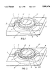
- FIG. 1 is a perspective of a single layer thickness field bulk acoustic wave resonator
- FIG. 2 is a perspective of a stack or multiple-layered thickness field bulk acoustic wave resonator
- FIG. 3 is a cross section through a lateral field device of the present invention.
- FIG. 4 is a top view of the device of FIG. 3;
- FIG. 5 lists in table format a number of III-V and II-VI binary and ternary compounds, and other piezoelectric semiconductor alloys, which can be used with the invention.
- the invention is directed to a semiconductor device which can be a III-V compound, a II-VI compound, or any other piezoelectric material or alloy.
- the preferred embodiment of the device architecture involves fabricating the same as a semi-insulating GaAs thin film on GaAs or AlGaAs substrate.
- the film orientation is preferably either along the 110! or the 111! crystal axis.
- the device is approximately 100 microns thick, so as to be MMIC compatible.
- the piezoelectrically active thin film (one or several layers stacked together) is 5 microns or thinner.
- the device's piezoelectrically active area edge is beveled for maximum Q and minimum spurious noise performance.
- the single layer device 12 is fabricated on a semi-insulating GaAs substrate 1, of the 110! or 111! orientation.
- the substrate 9 is approximately 100 microns thick, so as to be MMIC compatible.
- a gold transmission line 2 of 50 ohm characteristic impedance leading into the piezoelectrically active region 4 of the chip, which is located over the substrate 1.
- the gold transmission line extends only up to the thin film region 4 of the device 12.
- the 50 ohm gold transmission line 2 connects to implanted n+ GaAs transmission lines 5 and 10 which carry the signal in the thin film region of the device to the upper and lower electrodes 3 and 8, respectively.
- the connection to the top n+ transmission line 10 is made via an airbridge 7.
- the piezoelectrically active area of the device 12 is located between electrodes 3 and 8 in the vertical direction.
- the piezoelectric material 6 therefore exists between the electrodes 3 and 8.
- the piezoelectrically active area, electrodes 3 and 8, and implanted transmission lines 5 and 10 are disposed over the air via which enables the thin film structure 9.
- the bottom of the device has a ground plane 11, except under the air via underlying the thin film structure 9.
- the air via is formed by etching the semi-insulating GaAs until reaching an etch stop layer grown by molecular beam epitaxy (MBE), or other techniques.
- MBE molecular beam epitaxy
- the electrical connection to the top of the resonator, i.e. the active part of the chip, is from the gold transmission line 2, via the aforementioned gold airbridge 7.
- FIG. 2 illustrates a substantially similar multi-layer device 14 which is fabricated on a semi-insulating GaAs substrate layer 1, preferably on the 110! or 111! axis.
- the substrate 9 is approximately 100 microns thick, so as to be MMIC compatible.
- gold transmission lines 2 of 50 ohm characteristic impedance leading into the piezoelectrically active region (the resonator) of the chip.
- the gold transmission lines 2 extend only up to the thin film region of the device 14.
- the 50 ohm gold transmission lines connect to implanted n+ GaAs transmission lines 5 and 10 which carry the signal in the thin film region of the device to the upper electrode 3 and lower electrode 110.
- the connection to the top n+ transmission line 10 is made via an airbridge 7.
- the piezoelectrically active area of the device 14 is located between the multiple electrode/piezoelectric material stacked layers in the vertical direction.
- the piezoelectric materials 6 and 120 extend between the electrodes 3 and 110.
- the piezoelectrically active area, the electrodes 3 and 110 and implanted transmission lines 5 and 10 are disposed over the air via, which enables the thin film structure 8.
- the bottom of the device has a ground plane 11, except under the air via.
- the air via is formed by etching the semi-insulting GaAs until reaching an etch stop layer grown by MBE, or other technique. Connection is made to the top of the resonator from the gold transmission line by a gold airbridge 7.
- the acoustic resonator of FIG. 1 or FIG. 2 functions by reacting to an electric field generated between the upper and lower electrodes.
- the electric field excites several modes in the case of the 111! substrate orientation.
- the highest frequency of operation is given by the longitudinal mode, which is governed by:
- n is the harmonic number
- t is the film thickness in mm
- ⁇ is the density
- the fundamental frequency will be 1.04 GHz
- the fundamental frequency will be 5.2 GHz, using the second equation above. Note that for the multiple-layer structure (FIG. 2), a single layer thickness of 0.1 ⁇ m or lower is readily achievable, which leads to a fundamental resonance frequency in excess of 50 GHz.
- FIG. 5 A number of III-V and II-VI binary and ternary compounds, and other piezoelectric semiconductor alloys, which can be used for the purposes of the present invention, are disclosed in FIG. 5.
- the present invention realizes the fabrication of a thin film structure on GaAs/III-V or II-VI compounds, instead of using quartz, zinc oxide, or aluminum nitride.
- the invention uses the piezoelectric properties of the 110! and/or 111! substrate of class III-V semiconductors for a piezoelectrically active device, instead of a thin film overlay structure.
- the invention realizes an MMIC-compatible device structure.
- the use of very thin semiconductor electrodes obviates electrode mass-loading (which decreases the Q and has other disadvantages).
- the fundamental mode maximizes the piezoelectric coupling (compared to harmonic mode operation).
- the effective coupling decreases as the square of the harmonic number, so, for example, the third harmonic has only (1/9) or about 11% of the coupling on the fundamental.
- Limitation to the fundamental mode permits useful operation at microwave frequencies, but necessitates careful control of the manufacturing processes to assure flatness and parallelism, so that one has clean mode spectra, i.e., the graphs of resonator admittance versus frequency have sharply resonant single peaks, uncluttered by auxiliary resonances adjacent to the desired resonant peaks, leading to interference in operation.
- the semiconductor device 16 can be a III-IV compound, II-VI compound, or any other piezoelectric material, or alloy.
- the device architecture is fabricated on semi-insulating III-V compound such as a GaAs substrate 20 whose major surfaces are perpendicular to a certain crystal axis, such as the 100! axis.
- the device's active area or resonance structure 26 is a contoured, trapped-energy bulk wave resonator using the lateral-field excitation of the preferred 100! orientation of GaAs.
- the substrate 20 is approximately 100 microns thick, so as to be MMIC compatible, with a piezoelectrically active area thin film thickness of less than 5 microns.
- a gold transmission line 22 of 50 ohm characteristic impedance leading into the active region of the chip.
- the gold transmission line 22 only extends up to the thin film region of the device which is constituted of the region 34 (FIG. 4).
- the gold transmission line 22 connect to an implanted n+ GaAs transmission line 24 which carries the signal in the thin film region of the device to the electrodes 28.
- the piezoelectrically active area 26 of the device 16 is located between the electrodes 28, and is exposed to the driving electric field, which exists between these electrodes, in a lateral direction relative to the film thickness.
- the piezoelectrically active area 26, electrodes 28 and implanted transmission lines 24 are located over the air via 32, which enables the thin film structure to be excited piezoelectrically.
- the bottom of the device 16 has a ground plane 30, except under the air via 32.
- the acoustic resonator device 16 of FIGS. 3 and 4 is excited laterally by the pair of electrodes 28 which are located on either side of the thin active film 26. This produces excitation of the thickness shear or thickness extensional mode of the film.
- the signal is coupled out of the resonator device 16 through the transmission lines 24.
- f n (n/2t) ⁇ (C*/ ⁇ )
- n the overtone number
- t the film thickness
- ⁇ the mass density
- C the effective stiffness constant of the particular mode excited.
- f the thickness of the piezoelectrically active area.
- III-V and II-VI binary compounds and ternary, and other piezoelectric semiconductor alloys which can be used for the device of the present invention. These materials are listed in FIG. 5.
- Novel aspects of the device 16 include the provision of the thin film structure on GaAs/III-IV or II-VI compounds instead using quartz, zinc oxide, or aluminum nitride.
- the use of the piezoelectric property of the 100! axis of class III-V semiconductors for the piezoelectrically active device, instead of a thin film overlay structure is believed to be novel. So is the provision of an MMIC-compatible device structure and the implementation of a lateral-field piezoelectric excitation of acoustic modes using implanted n+ electrodes so that electrode mass loading (which decreases the Q and has other disadvantages) is obviated.
- using lateral-field excitation (LFE) gives an additional degree of design freedom. This is because it allows the lateral azimuth in the plane in the thin film to be selected so as to optimize one of the resonator properties, for example, to permit operation simultaneously on more than one thickness mode, or to permit discrimination against an unwanted interfering mode.
- the fundamental mode maximizes the piezoelectric coupling (compared to harmonic mode operation).
- the effect of coupling decreases as the square of the harmonic number, so, for example, the third harmonic has only (1/9) or about 11% of the coupling on the fundamental.
- Limitation to the fundamental mode permits use for operation at microwave frequencies, although it necessitates careful control of the manufacturing processes to assure flatness and parallelism, so that one has clean mode spectra, i.e. graphs of resonator admittance versus frequency that have sharply resonant single peaks, unclogged by auxiliary resonances adjacent to the desired resonant peaks, leading to interference in operation.
Abstract
The invention is directed to resonators and more particularly to an MMIC-compatible resonator which can be fabricated on an MMIC chip using MMIC processing techniques. The MMIC-compatible resonator has a substrate approximately 100 microns thick made of semi-insulating GaAs and/or AlGaAs. The substrate flanks an air via on which is fabricated a thin film piezoelectric semi-insulating GaAs film, comprising the piezoelectrically active element. The piezoelectrically active element is flanked either laterally or from the top to bottom thereof by a pair of electrodes which serve to excite the thickness shear or thickness extensional mode of the thin film piezoelectrically active element. There are a number of III-V and II-VI binary compounds and ternary, and other piezoelectric semiconductor alloys, which can be used for the purposes of the invention. The thin film measures approximately 5 microns or less in thickness and is fabricated on the semi-insulating GaAs, on the 110!, 111! or 100! axis thereof.
Description
The invention described herein may be manufactured, used, imported and licensed by or for the Government of the United States of America without the payment to us of any royalties thereon.
This invention relates to resonators and more particularly to a monolithic microwave integrated circuit (MMIC)-compatible resonator which can be fabricated on an MMIC chip using MMIC processing techniques.
Heretofore, a multitude of varying microwave/millimeter wave (MW/MMW) oscillators, filters, monolithic microwave integrated circuits (MMICs), resonators, phase lock loops and clock recovery circuits have been generally known to those skilled in the art. Despite the obvious advantages of these known devices, the prior art has thus far failed to provide to the trade a small size, compact, and MMIC compatible resonator having fundamental mode operation and high Q at MW/MMW frequencies. The present invention addresses this need.
Accordingly, it is an object of the present invention to provide such a small size, compact and MMIC compatible resonator having fundamental mode operation and high Q at MW/MMW frequencies.
It is a further object of the invention to provide a device which enables the fabrication of stable MW/MMW clock circuits.
It is a further object of the invention to provide an MMIC-compatible resonator which can be fabricated on an MMIC chip using MMIC processing techniques.
It is yet another object of the present invention to provide a method of reducing phase noise at the millimeter wave length by establishing high Q and tunable resonators, by providing monolithic bulk acoustic wave resonators that have fundamental operation at the MW/MMW frequencies.
A still further object of the present invention is to provide high quality factor resonators, tunable resonators, and stack filters for use in low phase noise oscillators, such as in high Q oscillators, as well as in tunable oscillators. Other applications include the provision of high frequency clock circuits.
The foregoing and other objects of the present invention are realized through the provision of a fundamental mode, high Q, MMIC-compatible monolithic resonator on a MMIC circuit, such as an oscillator. As a result of the invention, substantial size reduction can be obtained in: the size of the circuit, the size of the resonator, in some cases the resonator cavity, as well as in the hardware for the multiplication of a low frequency high Q resonant oscillator. Another advantage of the invention is that the circuit is contained on a single monolithic chip. The resonator is MMIC fabrication-compatible. It has a controllable resonant frequency due to layer growth and can be tuned via an external voltage for a VCO application.
Essentially, the invention comprises a monolithic microwave integrated circuit, i.e. a semiconductor device, which includes a substrate and an air via, wherein the substrate flanks the air via. A piezoelectrically active, thin film region is located above the air via and includes a piezoelectrically active element. A pair of electrodes flank the piezoelectrically active element and are designed to carry a signal which excites the piezoelectrically active element. A gold transmission line disposed over the substrate carries a signal to the electrodes, preferably through transmission lines which are implanted in the piezoelectrically active, thin film region.
The electrodes can flank the piezoelectrically active element by being disposed above and below it, relative to the thickness dimension of the piezoelectrically active element or, alternatively, the electrodes can flank the piezoelectrically active element laterally, in either case exciting a thickness shear or a thickness extensional mode of the active element. The semiconductor device has an overall thickness on the order of about 100 microns, in contrast to the piezoelectrically active thin film region which has a thickness of 5 microns or less. The piezoelectrically active element can be fabricated as a component of an oscillator, filter, monolithic microwave integrated circuit, phase lock loop, a clock recovery circuit or the like, or as a discrete resonator.
Other features and advantages of the present invention will become apparent from the following Detailed Description of the Invention which refers to the accompanying drawings wherein:
FIG. 1 is a perspective of a single layer thickness field bulk acoustic wave resonator;
FIG. 2 is a perspective of a stack or multiple-layered thickness field bulk acoustic wave resonator;
FIG. 3 is a cross section through a lateral field device of the present invention;
FIG. 4 is a top view of the device of FIG. 3; and
FIG. 5 lists in table format a number of III-V and II-VI binary and ternary compounds, and other piezoelectric semiconductor alloys, which can be used with the invention.
The invention is directed to a semiconductor device which can be a III-V compound, a II-VI compound, or any other piezoelectric material or alloy. The preferred embodiment of the device architecture involves fabricating the same as a semi-insulating GaAs thin film on GaAs or AlGaAs substrate. The film orientation is preferably either along the 110! or the 111! crystal axis. The device is approximately 100 microns thick, so as to be MMIC compatible. However, the piezoelectrically active thin film (one or several layers stacked together) is 5 microns or thinner. The device's piezoelectrically active area edge is beveled for maximum Q and minimum spurious noise performance.
With reference to FIG. 1, the single layer device 12 is fabricated on a semi-insulating GaAs substrate 1, of the 110! or 111! orientation. The substrate 9 is approximately 100 microns thick, so as to be MMIC compatible. On top of the substrate 1 is a gold transmission line 2 of 50 ohm characteristic impedance leading into the piezoelectrically active region 4 of the chip, which is located over the substrate 1. The gold transmission line extends only up to the thin film region 4 of the device 12. The 50 ohm gold transmission line 2 connects to implanted n+ GaAs transmission lines 5 and 10 which carry the signal in the thin film region of the device to the upper and lower electrodes 3 and 8, respectively. The connection to the top n+ transmission line 10 is made via an airbridge 7. The piezoelectrically active area of the device 12 is located between electrodes 3 and 8 in the vertical direction. The piezoelectric material 6 therefore exists between the electrodes 3 and 8.
The piezoelectrically active area, electrodes 3 and 8, and implanted transmission lines 5 and 10 are disposed over the air via which enables the thin film structure 9. The bottom of the device has a ground plane 11, except under the air via underlying the thin film structure 9. The air via is formed by etching the semi-insulating GaAs until reaching an etch stop layer grown by molecular beam epitaxy (MBE), or other techniques. The electrical connection to the top of the resonator, i.e. the active part of the chip, is from the gold transmission line 2, via the aforementioned gold airbridge 7.
FIG. 2 illustrates a substantially similar multi-layer device 14 which is fabricated on a semi-insulating GaAs substrate layer 1, preferably on the 110! or 111! axis. As before, the substrate 9 is approximately 100 microns thick, so as to be MMIC compatible. On top of the device are gold transmission lines 2 of 50 ohm characteristic impedance leading into the piezoelectrically active region (the resonator) of the chip. The gold transmission lines 2 extend only up to the thin film region of the device 14. The 50 ohm gold transmission lines connect to implanted n+ GaAs transmission lines 5 and 10 which carry the signal in the thin film region of the device to the upper electrode 3 and lower electrode 110. The connection to the top n+ transmission line 10 is made via an airbridge 7. The piezoelectrically active area of the device 14 is located between the multiple electrode/piezoelectric material stacked layers in the vertical direction.
The piezoelectric materials 6 and 120 extend between the electrodes 3 and 110. The piezoelectrically active area, the electrodes 3 and 110 and implanted transmission lines 5 and 10 are disposed over the air via, which enables the thin film structure 8. The bottom of the device has a ground plane 11, except under the air via. The air via is formed by etching the semi-insulting GaAs until reaching an etch stop layer grown by MBE, or other technique. Connection is made to the top of the resonator from the gold transmission line by a gold airbridge 7.
In operation, the acoustic resonator of FIG. 1 or FIG. 2 functions by reacting to an electric field generated between the upper and lower electrodes. The electric field excites several modes in the case of the 111! substrate orientation. The highest frequency of operation is given by the longitudinal mode, which is governed by:
f.sub.n =(n/2t)√ (C.sub.11 +2C.sub.12 +4C.sub.44)/3ρ!=2.755 n/t (MHz*mm);
where n is the harmonic number, t is the film thickness in mm, and ρ is the density.
For 110! substrate orientation, the corresponding resonance frequency (longitudinal mode, thickness field excitation) is given by:
f.sub.n =(n/2t)√ (C.sub.11 +C.sub.12 +2C.sub.44)/ρ!=5.2 n/t (MHz*mm).
Thus, for a 110! film of 5 μm thickness, the fundamental frequency will be 1.04 GHz, and for a 110! film 1 μm thick, the fundamental frequency will be 5.2 GHz, using the second equation above. Note that for the multiple-layer structure (FIG. 2), a single layer thickness of 0.1 μm or lower is readily achievable, which leads to a fundamental resonance frequency in excess of 50 GHz.
A number of III-V and II-VI binary and ternary compounds, and other piezoelectric semiconductor alloys, which can be used for the purposes of the present invention, are disclosed in FIG. 5.
Thus, in a novel manner, the present invention realizes the fabrication of a thin film structure on GaAs/III-V or II-VI compounds, instead of using quartz, zinc oxide, or aluminum nitride. The invention uses the piezoelectric properties of the 110! and/or 111! substrate of class III-V semiconductors for a piezoelectrically active device, instead of a thin film overlay structure. And in a previously unknown manner, the invention realizes an MMIC-compatible device structure. The use of very thin semiconductor electrodes obviates electrode mass-loading (which decreases the Q and has other disadvantages).
Use of the fundamental mode (film thickness being one-half an acoustic wavelength) maximizes the piezoelectric coupling (compared to harmonic mode operation). The effective coupling decreases as the square of the harmonic number, so, for example, the third harmonic has only (1/9) or about 11% of the coupling on the fundamental. Limitation to the fundamental mode permits useful operation at microwave frequencies, but necessitates careful control of the manufacturing processes to assure flatness and parallelism, so that one has clean mode spectra, i.e., the graphs of resonator admittance versus frequency have sharply resonant single peaks, uncluttered by auxiliary resonances adjacent to the desired resonant peaks, leading to interference in operation.
In the alternate embodiment of the invention shown in FIGS. 3 and 4, the semiconductor device 16 can be a III-IV compound, II-VI compound, or any other piezoelectric material, or alloy. The device architecture is fabricated on semi-insulating III-V compound such as a GaAs substrate 20 whose major surfaces are perpendicular to a certain crystal axis, such as the 100! axis. The device's active area or resonance structure 26 is a contoured, trapped-energy bulk wave resonator using the lateral-field excitation of the preferred 100! orientation of GaAs.
Preferably, the substrate 20 is approximately 100 microns thick, so as to be MMIC compatible, with a piezoelectrically active area thin film thickness of less than 5 microns. On top of the device 16 is a gold transmission line 22 of 50 ohm characteristic impedance leading into the active region of the chip. The gold transmission line 22 only extends up to the thin film region of the device which is constituted of the region 34 (FIG. 4). The gold transmission line 22 connect to an implanted n+ GaAs transmission line 24 which carries the signal in the thin film region of the device to the electrodes 28. The piezoelectrically active area 26 of the device 16 is located between the electrodes 28, and is exposed to the driving electric field, which exists between these electrodes, in a lateral direction relative to the film thickness. The piezoelectrically active area 26, electrodes 28 and implanted transmission lines 24 are located over the air via 32, which enables the thin film structure to be excited piezoelectrically. The bottom of the device 16 has a ground plane 30, except under the air via 32.
Unlike the previously described devices 12 and 14 which are excited vertically, the acoustic resonator device 16 of FIGS. 3 and 4 is excited laterally by the pair of electrodes 28 which are located on either side of the thin active film 26. This produces excitation of the thickness shear or thickness extensional mode of the film. The signal is coupled out of the resonator device 16 through the transmission lines 24.
The operation at any harmonic mode produces a frequency, fn, where fn =(n/2t)√(C*/ρ), and where n is the overtone number, t is the film thickness, ρ is the mass density and C is the effective stiffness constant of the particular mode excited. To increase the operational frequency, one can decrease the thickness t of the piezoelectrically active area. As an example, for a GaAs active area, the fundamental frequency is given by f=1.671/t (MHz*mm). Therefore, for t equals 5 micrometers, f equals 340 MHz. For t of 1 micrometer, f equals to 1.7 GHz. One of the advantages of using lateral field excitation is that there is no direct contact between the electrodes and the vibrating region, which leads to decreased damping and hence an increased quality factor of the resonator.
As before, there are a number of III-V and II-VI binary compounds and ternary, and other piezoelectric semiconductor alloys, which can be used for the device of the present invention. These materials are listed in FIG. 5.
Novel aspects of the device 16 include the provision of the thin film structure on GaAs/III-IV or II-VI compounds instead using quartz, zinc oxide, or aluminum nitride. Similarly, the use of the piezoelectric property of the 100! axis of class III-V semiconductors for the piezoelectrically active device, instead of a thin film overlay structure, is believed to be novel. So is the provision of an MMIC-compatible device structure and the implementation of a lateral-field piezoelectric excitation of acoustic modes using implanted n+ electrodes so that electrode mass loading (which decreases the Q and has other disadvantages) is obviated. In addition, using lateral-field excitation (LFE) gives an additional degree of design freedom. This is because it allows the lateral azimuth in the plane in the thin film to be selected so as to optimize one of the resonator properties, for example, to permit operation simultaneously on more than one thickness mode, or to permit discrimination against an unwanted interfering mode.
Use of the fundamental mode (film thickness being one-half an acoustic wavelength) maximizes the piezoelectric coupling (compared to harmonic mode operation). The effect of coupling decreases as the square of the harmonic number, so, for example, the third harmonic has only (1/9) or about 11% of the coupling on the fundamental. Limitation to the fundamental mode permits use for operation at microwave frequencies, although it necessitates careful control of the manufacturing processes to assure flatness and parallelism, so that one has clean mode spectra, i.e. graphs of resonator admittance versus frequency that have sharply resonant single peaks, unclogged by auxiliary resonances adjacent to the desired resonant peaks, leading to interference in operation.
Although the present invention has been described in relation to particular embodiments thereof, many other variations and modifications and other uses will become apparent to those skilled in the art. It is preferred, therefore, that the present invention be limited not by the specific disclosure herein, but only by the appended claims.
Claims (16)
1. A monolithic microwave integrated circuit, semiconductor device, comprising:
a substrate and an air via, the substrate flanking the air via and being selected from the group of GaAs and AlGaAs;
a piezoelectrically active, semi-insulating GaAs thin film region located over the air via;
a piezoelectrically active element in the piezoelectrically active region;
a pair of electrodes flanking the piezoelectrically active element and effective for carrying a signal which excites the piezoelectrically active element; and
a transmission line over the substrate for carrying a signal to the electrodes.
2. The semiconductor device of claim 1, in which the semiconductor device has a thickness on the order of about 100 microns and the thin film region has a thickness not greater than about 5 microns.
3. The semiconductor device of claim 1, in which the electrodes flank the piezoelectrically active element by being disposed above and below the same, relative to a thickness dimension of the piezoelectrically active element.
4. The semiconductor device of claim 1, in which the electrodes laterally flank the piezoelectrically active element, in a manner which excites a thickness shear or a thickness extensional mode of the piezoelectrically active element.
5. The semiconductor device of claim 1, in which the piezoelectrically active element is formed as part of an MMIC circuit from the group of: oscillators, filters, monolithic microwave integrated circuits, resonators, phase lock loops and clock recovery circuits.
6. The semiconductor device of claim 1, in which a film orientation of the thin film region is along a 110! crystal axis.
7. The semiconductor device of claim 1, in which a film orientation of the thin film region is along a 111! crystal axis.
8. The semiconductor device of claim 1, in which the thin film region comprises a plurality of layers in the form of a multiple-layer thickness field bulk acoustic wave resonator.
9. The semiconductor device of claim 1, in which the transmission line is a gold transmission line of 50 ohm characteristic impedance which extends only up to the thin film region of the semiconductor device.
10. A monolithic microwave integrated circuit, semiconductor device, comprising:
a substrate and an air via, the substrate flanking the air via;
a piezoelectrically active, thin film region located over the air via;
a piezoelectrically active element in the piezoelectrically active region;
a pair of electrodes flanking the piezoelectrically active element and effective for carrying a signal which excites the piezoelectrically active element; and
a gold transmission line of 50 ohm characteristic impedance which extends over the substrate only up to the thin film region of the semiconductor device and connects to an n+ GaAs internal transmission line which carries a signal in the thin film region to the electrodes.
11. The semiconductor device of claim 10, further comprising an airbridge transmission line between the transmission line and the n+ GaAs transmission line.
12. The semiconductor device of claim 11, further including a ground plane on a bottom side of the substrate.
13. The semiconductor device of claim 1, in which the air via is formed by etching the semi-insulating GaAs until reaching an etch stop layer.
14. The semiconductor device of claim 1, in which the semiconductor device is constructed to have a fundamental frequency on the order of 1 GHz when a thickness of the thin film region is about 5 microns and a fundamental frequency of about 5 GHz when the thin film region has a thickness of about 1 micron.
15. The semiconductor device of claim 1, in which the thin film region has a thickness on the order of about 0.1 microns and a fundamental resonance frequency in excess of 50 GHz.
16. The semiconductor device of claim 1, in which the substrate is fabricated of a material selected from the group of: AlP, AlAs, AlSb, GaP, GaAs, GaSb, InP, InAs, InSb, In.53Ga.47As, AlGaAs, InGaAspIP and alloys thereof.
Priority Applications (1)
| Application Number | Priority Date | Filing Date | Title |
|---|---|---|---|
| US08/694,890 US5801476A (en) | 1996-08-09 | 1996-08-09 | Thickness mode acoustic wave resonator |
Applications Claiming Priority (1)
| Application Number | Priority Date | Filing Date | Title |
|---|---|---|---|
| US08/694,890 US5801476A (en) | 1996-08-09 | 1996-08-09 | Thickness mode acoustic wave resonator |
Publications (1)
| Publication Number | Publication Date |
|---|---|
| US5801476A true US5801476A (en) | 1998-09-01 |
Family
ID=24790678
Family Applications (1)
| Application Number | Title | Priority Date | Filing Date |
|---|---|---|---|
| US08/694,890 Expired - Fee Related US5801476A (en) | 1996-08-09 | 1996-08-09 | Thickness mode acoustic wave resonator |
Country Status (1)
| Country | Link |
|---|---|
| US (1) | US5801476A (en) |
Cited By (10)
| Publication number | Priority date | Publication date | Assignee | Title |
|---|---|---|---|---|
| US6028389A (en) * | 1998-05-26 | 2000-02-22 | The Charles Stark Draper Laboratory, Inc. | Micromachined piezoelectric transducer |
| US6271619B1 (en) * | 1997-05-13 | 2001-08-07 | Mitsubishi Denki Kabushiki Kaisha | Piezoelectric thin film device |
| US6306313B1 (en) | 2000-02-04 | 2001-10-23 | Agere Systems Guardian Corp. | Selective etching of thin films |
| US20020194005A1 (en) * | 2001-03-27 | 2002-12-19 | Lahr Roy J. | Head-worn, trimodal device to increase transcription accuracy in a voice recognition system and to process unvocalized speech |
| WO2003005576A1 (en) * | 2001-07-03 | 2003-01-16 | Epcos Ag | Frequency-tunable resonator |
| US6746577B1 (en) | 1999-12-16 | 2004-06-08 | Agere Systems, Inc. | Method and apparatus for thickness control and reproducibility of dielectric film deposition |
| US20060176126A1 (en) * | 2002-08-08 | 2006-08-10 | Li-Peng Wang | Manufacturing film bulk acoustic resonator filters |
| US20080247264A1 (en) * | 2005-09-09 | 2008-10-09 | Siemens Aktiengesellschaft | Apparatus and Method For Moving a Liquid by Means of a Piezoelectric Transducer |
| US20100107400A1 (en) * | 2006-05-17 | 2010-05-06 | Avago Technologies Wireless Ip (Singapore) Pte.Ltd | Method of manufacturing an acoustic mirror |
| CN104185822A (en) * | 2012-01-09 | 2014-12-03 | 芬顿系统有限公司 | A clock signal generator for a digital circuit |
Citations (7)
| Publication number | Priority date | Publication date | Assignee | Title |
|---|---|---|---|---|
| US4502932A (en) * | 1983-10-13 | 1985-03-05 | The United States Of America As Represented By The United States Department Of Energy | Acoustic resonator and method of making same |
| US5075641A (en) * | 1990-12-04 | 1991-12-24 | Iowa State University Research Foundation, Inc. | High frequency oscillator comprising cointegrated thin film resonator and active device |
| US5166646A (en) * | 1992-02-07 | 1992-11-24 | Motorola, Inc. | Integrated tunable resonators for use in oscillators and filters |
| US5185589A (en) * | 1991-05-17 | 1993-02-09 | Westinghouse Electric Corp. | Microwave film bulk acoustic resonator and manifolded filter bank |
| US5233259A (en) * | 1991-02-19 | 1993-08-03 | Westinghouse Electric Corp. | Lateral field FBAR |
| US5446306A (en) * | 1993-12-13 | 1995-08-29 | Trw Inc. | Thin film voltage-tuned semiconductor bulk acoustic resonator (SBAR) |
| US5552655A (en) * | 1994-05-04 | 1996-09-03 | Trw Inc. | Low frequency mechanical resonator |
-
1996
- 1996-08-09 US US08/694,890 patent/US5801476A/en not_active Expired - Fee Related
Patent Citations (7)
| Publication number | Priority date | Publication date | Assignee | Title |
|---|---|---|---|---|
| US4502932A (en) * | 1983-10-13 | 1985-03-05 | The United States Of America As Represented By The United States Department Of Energy | Acoustic resonator and method of making same |
| US5075641A (en) * | 1990-12-04 | 1991-12-24 | Iowa State University Research Foundation, Inc. | High frequency oscillator comprising cointegrated thin film resonator and active device |
| US5233259A (en) * | 1991-02-19 | 1993-08-03 | Westinghouse Electric Corp. | Lateral field FBAR |
| US5185589A (en) * | 1991-05-17 | 1993-02-09 | Westinghouse Electric Corp. | Microwave film bulk acoustic resonator and manifolded filter bank |
| US5166646A (en) * | 1992-02-07 | 1992-11-24 | Motorola, Inc. | Integrated tunable resonators for use in oscillators and filters |
| US5446306A (en) * | 1993-12-13 | 1995-08-29 | Trw Inc. | Thin film voltage-tuned semiconductor bulk acoustic resonator (SBAR) |
| US5552655A (en) * | 1994-05-04 | 1996-09-03 | Trw Inc. | Low frequency mechanical resonator |
Non-Patent Citations (4)
| Title |
|---|
| Acoustic Bulk Wave Composite Resonators, by Larkin et al, Appl. Phys. Lett 38(3), Feb. 1, 1981, pp. 125 127. * |
| Acoustic Bulk Wave Composite Resonators, by Larkin et al, Appl. Phys. Lett 38(3), Feb. 1, 1981, pp. 125-127. |
| Temperature Compensated High Coupling and High Quality Factor ZnO/SiO 2 Bulk Wave Resonators on High Resistance Substrates, by Shiosaki et al, IEEE Ultrasonics Symposium, 1984, pp. 405 410. * |
| Temperature Compensated High Coupling and High Quality Factor ZnO/SiO2ulk Wave Resonators on High Resistance Substrates, by Shiosaki et al, IEEE Ultrasonics Symposium, 1984, pp. 405-410. |
Cited By (15)
| Publication number | Priority date | Publication date | Assignee | Title |
|---|---|---|---|---|
| US6271619B1 (en) * | 1997-05-13 | 2001-08-07 | Mitsubishi Denki Kabushiki Kaisha | Piezoelectric thin film device |
| US6028389A (en) * | 1998-05-26 | 2000-02-22 | The Charles Stark Draper Laboratory, Inc. | Micromachined piezoelectric transducer |
| US6746577B1 (en) | 1999-12-16 | 2004-06-08 | Agere Systems, Inc. | Method and apparatus for thickness control and reproducibility of dielectric film deposition |
| US6306313B1 (en) | 2000-02-04 | 2001-10-23 | Agere Systems Guardian Corp. | Selective etching of thin films |
| US20020194005A1 (en) * | 2001-03-27 | 2002-12-19 | Lahr Roy J. | Head-worn, trimodal device to increase transcription accuracy in a voice recognition system and to process unvocalized speech |
| US20040212277A1 (en) * | 2001-07-03 | 2004-10-28 | Ralph Stommer | Frequency-tunable resonator |
| WO2003005576A1 (en) * | 2001-07-03 | 2003-01-16 | Epcos Ag | Frequency-tunable resonator |
| US7098573B2 (en) | 2001-07-03 | 2006-08-29 | Epcos Ag | Frequency-tunable resonator |
| US20060176126A1 (en) * | 2002-08-08 | 2006-08-10 | Li-Peng Wang | Manufacturing film bulk acoustic resonator filters |
| US20080247264A1 (en) * | 2005-09-09 | 2008-10-09 | Siemens Aktiengesellschaft | Apparatus and Method For Moving a Liquid by Means of a Piezoelectric Transducer |
| US8240907B2 (en) * | 2005-09-09 | 2012-08-14 | Siemens Aktiengesellschaft | Apparatus and method for moving a liquid by means of a piezoelectric transducer |
| US20100107400A1 (en) * | 2006-05-17 | 2010-05-06 | Avago Technologies Wireless Ip (Singapore) Pte.Ltd | Method of manufacturing an acoustic mirror |
| US8256093B2 (en) | 2006-05-17 | 2012-09-04 | Avago Technologies Wireless Ip (Singapore) Pte. Ltd. | Method of manufacturing an acoustic mirror |
| CN104185822A (en) * | 2012-01-09 | 2014-12-03 | 芬顿系统有限公司 | A clock signal generator for a digital circuit |
| CN108170204A (en) * | 2012-01-09 | 2018-06-15 | 芬顿系统有限公司 | A kind of clock-signal generator for digital circuit |
Similar Documents
| Publication | Publication Date | Title |
|---|---|---|
| CA2283887C (en) | Film bulk acoustic wave device | |
| US6424237B1 (en) | Bulk acoustic resonator perimeter reflection system | |
| US5884378A (en) | Method of making an enhanced quality factor resonator | |
| US5789845A (en) | Film bulk acoustic wave device | |
| US5373268A (en) | Thin film resonator having stacked acoustic reflecting impedance matching layers and method | |
| US6548942B1 (en) | Encapsulated packaging for thin-film resonators and thin-film resonator-based filters having a piezoelectric resonator between two acoustic reflectors | |
| US5617065A (en) | Filter using enhanced quality factor resonator and method | |
| US6437484B1 (en) | Piezoelectric resonator | |
| US5023503A (en) | Super high frequency oscillator/resonator | |
| US20040195937A1 (en) | Film bulk acoustic resonator and film bulk acoustic resonator circuit | |
| EP0771070B1 (en) | A film bulk acoustic wave device | |
| US7423501B2 (en) | Film bulk acoustic wave resonator and manufacturing method thererof | |
| US6603241B1 (en) | Acoustic mirror materials for acoustic devices | |
| EP1434346A1 (en) | Piezoelectric resonant filter and duplexer | |
| EP0823780A1 (en) | Electro-acoustic hybrid integrated circuit and manufacturing method thereof | |
| US20070240294A1 (en) | MEMS piezoelectric longitudinal mode resonator | |
| US5801476A (en) | Thickness mode acoustic wave resonator | |
| US6870446B2 (en) | High frequency filter | |
| US4743874A (en) | Magnetostatic wave tunable resonator | |
| US4983937A (en) | Magnetostatic wave band-pass-filter | |
| JPH0450766B2 (en) | ||
| CN112702038A (en) | Tunable solid-mounted bulk acoustic wave resonator | |
| US20230006635A1 (en) | Acoustic resonator | |
| TWI794053B (en) | Bulk acoustic resonator | |
| JP2003158442A (en) | Piezoelectric thin film resonator element and filter using the same |
Legal Events
| Date | Code | Title | Description |
|---|---|---|---|
| AS | Assignment |
Owner name: ARMY, THE GOVERNMENT OF THE UNITED STATES OF AMERI Free format text: ASSIGNMENT OF ASSIGNORS INTEREST;ASSIGNORS:STURZEBECHER, DANA J.;KOSINSKI, JOHN A.;BALLAT, ARTHUR;REEL/FRAME:009256/0167;SIGNING DATES FROM 19960731 TO 19960801 |
|
| REMI | Maintenance fee reminder mailed | ||
| FPAY | Fee payment |
Year of fee payment: 4 |
|
| SULP | Surcharge for late payment | ||
| REMI | Maintenance fee reminder mailed | ||
| LAPS | Lapse for failure to pay maintenance fees | ||
| STCH | Information on status: patent discontinuation |
Free format text: PATENT EXPIRED DUE TO NONPAYMENT OF MAINTENANCE FEES UNDER 37 CFR 1.362 |
|
| FP | Lapsed due to failure to pay maintenance fee |
Effective date: 20060901 |