US5867236A - Construction and sealing of tiled, flat-panel displays - Google Patents
Construction and sealing of tiled, flat-panel displays Download PDFInfo
- Publication number
- US5867236A US5867236A US08/652,032 US65203296A US5867236A US 5867236 A US5867236 A US 5867236A US 65203296 A US65203296 A US 65203296A US 5867236 A US5867236 A US 5867236A
- Authority
- US
- United States
- Prior art keywords
- tiles
- panel display
- substantially flat
- accordance
- backplate
- Prior art date
- Legal status (The legal status is an assumption and is not a legal conclusion. Google has not performed a legal analysis and makes no representation as to the accuracy of the status listed.)
- Expired - Lifetime
Links
Images


Classifications
-
- G—PHYSICS
- G02—OPTICS
- G02F—OPTICAL DEVICES OR ARRANGEMENTS FOR THE CONTROL OF LIGHT BY MODIFICATION OF THE OPTICAL PROPERTIES OF THE MEDIA OF THE ELEMENTS INVOLVED THEREIN; NON-LINEAR OPTICS; FREQUENCY-CHANGING OF LIGHT; OPTICAL LOGIC ELEMENTS; OPTICAL ANALOGUE/DIGITAL CONVERTERS
- G02F1/00—Devices or arrangements for the control of the intensity, colour, phase, polarisation or direction of light arriving from an independent light source, e.g. switching, gating or modulating; Non-linear optics
- G02F1/01—Devices or arrangements for the control of the intensity, colour, phase, polarisation or direction of light arriving from an independent light source, e.g. switching, gating or modulating; Non-linear optics for the control of the intensity, phase, polarisation or colour
- G02F1/13—Devices or arrangements for the control of the intensity, colour, phase, polarisation or direction of light arriving from an independent light source, e.g. switching, gating or modulating; Non-linear optics for the control of the intensity, phase, polarisation or colour based on liquid crystals, e.g. single liquid crystal display cells
- G02F1/133—Constructional arrangements; Operation of liquid crystal cells; Circuit arrangements
- G02F1/1333—Constructional arrangements; Manufacturing methods
- G02F1/1339—Gaskets; Spacers; Sealing of cells
-
- G—PHYSICS
- G06—COMPUTING; CALCULATING OR COUNTING
- G06F—ELECTRIC DIGITAL DATA PROCESSING
- G06F3/00—Input arrangements for transferring data to be processed into a form capable of being handled by the computer; Output arrangements for transferring data from processing unit to output unit, e.g. interface arrangements
- G06F3/14—Digital output to display device ; Cooperation and interconnection of the display device with other functional units
- G06F3/1423—Digital output to display device ; Cooperation and interconnection of the display device with other functional units controlling a plurality of local displays, e.g. CRT and flat panel display
- G06F3/1446—Digital output to display device ; Cooperation and interconnection of the display device with other functional units controlling a plurality of local displays, e.g. CRT and flat panel display display composed of modules, e.g. video walls
-
- G—PHYSICS
- G09—EDUCATION; CRYPTOGRAPHY; DISPLAY; ADVERTISING; SEALS
- G09F—DISPLAYING; ADVERTISING; SIGNS; LABELS OR NAME-PLATES; SEALS
- G09F9/00—Indicating arrangements for variable information in which the information is built-up on a support by selection or combination of individual elements
- G09F9/30—Indicating arrangements for variable information in which the information is built-up on a support by selection or combination of individual elements in which the desired character or characters are formed by combining individual elements
- G09F9/302—Indicating arrangements for variable information in which the information is built-up on a support by selection or combination of individual elements in which the desired character or characters are formed by combining individual elements characterised by the form or geometrical disposition of the individual elements
- G09F9/3026—Video wall, i.e. stackable semiconductor matrix display modules
-
- G—PHYSICS
- G09—EDUCATION; CRYPTOGRAPHY; DISPLAY; ADVERTISING; SEALS
- G09G—ARRANGEMENTS OR CIRCUITS FOR CONTROL OF INDICATING DEVICES USING STATIC MEANS TO PRESENT VARIABLE INFORMATION
- G09G3/00—Control arrangements or circuits, of interest only in connection with visual indicators other than cathode-ray tubes
- G09G3/20—Control arrangements or circuits, of interest only in connection with visual indicators other than cathode-ray tubes for presentation of an assembly of a number of characters, e.g. a page, by composing the assembly by combination of individual elements arranged in a matrix no fixed position being assigned to or needed to be assigned to the individual characters or partial characters
-
- G—PHYSICS
- G02—OPTICS
- G02F—OPTICAL DEVICES OR ARRANGEMENTS FOR THE CONTROL OF LIGHT BY MODIFICATION OF THE OPTICAL PROPERTIES OF THE MEDIA OF THE ELEMENTS INVOLVED THEREIN; NON-LINEAR OPTICS; FREQUENCY-CHANGING OF LIGHT; OPTICAL LOGIC ELEMENTS; OPTICAL ANALOGUE/DIGITAL CONVERTERS
- G02F1/00—Devices or arrangements for the control of the intensity, colour, phase, polarisation or direction of light arriving from an independent light source, e.g. switching, gating or modulating; Non-linear optics
- G02F1/01—Devices or arrangements for the control of the intensity, colour, phase, polarisation or direction of light arriving from an independent light source, e.g. switching, gating or modulating; Non-linear optics for the control of the intensity, phase, polarisation or colour
- G02F1/13—Devices or arrangements for the control of the intensity, colour, phase, polarisation or direction of light arriving from an independent light source, e.g. switching, gating or modulating; Non-linear optics for the control of the intensity, phase, polarisation or colour based on liquid crystals, e.g. single liquid crystal display cells
- G02F1/133—Constructional arrangements; Operation of liquid crystal cells; Circuit arrangements
- G02F1/1333—Constructional arrangements; Manufacturing methods
- G02F1/13336—Combining plural substrates to produce large-area displays, e.g. tiled displays
-
- G—PHYSICS
- G09—EDUCATION; CRYPTOGRAPHY; DISPLAY; ADVERTISING; SEALS
- G09G—ARRANGEMENTS OR CIRCUITS FOR CONTROL OF INDICATING DEVICES USING STATIC MEANS TO PRESENT VARIABLE INFORMATION
- G09G2300/00—Aspects of the constitution of display devices
- G09G2300/02—Composition of display devices
- G09G2300/026—Video wall, i.e. juxtaposition of a plurality of screens to create a display screen of bigger dimensions
-
- G—PHYSICS
- G09—EDUCATION; CRYPTOGRAPHY; DISPLAY; ADVERTISING; SEALS
- G09G—ARRANGEMENTS OR CIRCUITS FOR CONTROL OF INDICATING DEVICES USING STATIC MEANS TO PRESENT VARIABLE INFORMATION
- G09G2300/00—Aspects of the constitution of display devices
- G09G2300/04—Structural and physical details of display devices
- G09G2300/0421—Structural details of the set of electrodes
- G09G2300/0426—Layout of electrodes and connections
Definitions
- the invention pertains to the field of flat-panel displays (FPDs) and, more particularly, to the construction and sealing of large, monolithically-addressed, flat-panel displays having a plurality of display "tiles".
- FPDs flat-panel displays
- Monolithic displays are used predominantly in laptop and portable computers of diagonal sizes of up to 12 inches. They have recently been introduced in desktop personal computers, as well as small televisions. In these applications, a frame surrounds the edge of the glass panels containing the active display elements, i.e., active-matrix liquid-crystal displays (AMLCDs).
- AMLCDs active-matrix liquid-crystal displays
- Seals for liquid-crystal displays are located at the perimeter thereof and are covered by the frame and housing. Such seals provide a mechanical joint between the top and bottom glass plates of the FPD, as well as contain the liquid-crystal material between the plates. Although the seals are usually polymeric adhesives, a small quantity of glass (or alternative material) spacers contained therein maintains a desired separation distance between the top and bottom plates. Characteristically, this distance between plates ranges from a few microns to 15 microns or more. Typical widths of the seals themselves are customarily a few millimeters.
- the polymeric adhesives are usually epoxy-based, thus having a solubility for water and a diffusivity that is appreciable enough to permit water permeation over extended periods of time (days to months).
- the desired size of seals for individual AMLCD tiles may be an order of magnitude narrower than 1 millimeter; however, the seals for AMLCD FPDs have been proven to be reliable only for widths of 1 millimeter or wider.
- the rate of diffusion increases exponentially with the reciprocal of the width of the seal, as well as in proportion to the seal thickness and the diffusivity constant for the seal material.
- the seals perform several functions, as aforementioned. They mechanically hold the top plate and the bottom plate of the AMLCD in register (both vertically and horizontally), while also providing robustness to the optical stack.
- the adhesive forms the walls of a reservoir to hold the liquid-crystal material, protecting it from the ambient humidity which may degrade or change its optical properties.
- the adhesive seal along with spacers, provides a sustaining force to maintain the glass plates essentially parallel to each other and uniformly spaced with respect to one another.
- This spacing is important for uniform electro-optical response, which is determined by a liquid crystal's electric field that is generated by two respective plates, an anode and a cathode, one on each glass plate.
- AMLCDs that are made up of a plurality of individual tiles may need unique sealing designs.
- Seal width is a major contributor to seam width, since there are two seals in a seam width, i.e, one on each tile perimeter. The more narrow the seam, the more efficient the light transmission is for viewing, and the easier it is to mask and modify the optical properties of the seam. In fact, narrow seals and seams in tiled displays allow for conventionally smaller pixel pitch, hence resulting in displays of greater resolution.
- tiled displays may need special attention to mechanical design, for the reliability of the individual tiles must be ensured, so as to prevent any effects from humid environments and provide forces maintaining the registration of the top and bottom plates of the AMLCD.
- the edge dimensions thereof are preferably maintained so that the interpixel spacing remains uniformly periodic throughout the tiles and across the seams, and the pitch minimized from tile to tile, as well as within each tile. Nevertheless, sealing integrity and reliability must be maintained for all of the display's tile edges.
- the tile perimeter design elements incorporated into the dark, interpixel space include:
- the liquid-crystal material in tiled, flat-panel displays has the same susceptibility to moisture as do monolithic, liquid-crystal displays, but the design and manufacturing problems become more thorny.
- the need for invisible seams between any one tile and its adjacent tiles results in the need to keep all dimensions in this area, including the width of the adhesive seal, extremely small (approximately a few tenths of a millimeter, at most).
- Electrical connection to the display is usually achieved by utilizing flexible connections, either from a printed circuit board containing drive and addressing electronics, or with an integrated-function chip carrier/flexible cable design. In either case, such electrical connection decreases the space available for sealing for a given pixel pitch.
- U.S. Pat. No. 5,668,569 described the advantage of positioning row and column drivers at a common edge of a tile and to deliver row and column signals to the tile from the common edge. This may eliminate the need for electrical connections at narrow ledges of interior tiles in a FPD of tiles 2 ⁇ N, where N>2. This in turn may improve optical performance of the display.
- tile edges corresponding with the display's perimeter edges are designed with a wide seal. Interior edges, however, have narrow seals in order to maintain the desired, constant, pixel pitch across tile boundaries.
- this invention applies specifically to arrays of tiles 2 ⁇ 2 or less, and, in other cases, to N ⁇ M arrays, where N and M are any integer numbers.
- the tiles may be enclosed with top and bottom glass plates, which are sealed with an adhesive bond to the tiles on the outside perimeter of the tiled display.
- Vertical seams (where tiles meet at the perimeter of the FPD) are sealed with a small amount of polymer.
- the seal may be constructed between a cover plate and a back plate, sandwiching the tiles.
- the AMLCD edges may be coated with either a non-permeable material or a polymer having an extremely low permeability (e.g., ParyleneTM). Another example is liquid-crystal polymer.
- edge sealing of individual tiles can be achieved by using a metallized film adhesive that is bonded to the tile edges.
- a low-temperature, sintered Solgel can be used to achieve extremely narrow, yet mechanically strong, seals for individual tiles.
- Still another enhancement employs a metallurgical seal outside a narrow, polymer seal.
- This invention also addresses processes for filling tiles with liquid-crystal material, so as to improve the optical seamlessness at tile boundaries. Also disclosed herein are designs for providing driver line inputs to all tiles in a tiled display, enabling the testing and verification of tiles prior to any further assembly.
- this invention addresses the construction of the optical and structural elements of a tiled, flat-panel display, as well as methods of maintaining the coplanarity of viewing surfaces.
- this invention addresses methods of providing row- and column-driver inputs to each tile in a tiled display.
- this invention addresses methods to allow testing of tiles to assure quality before assembling tiled arrays.
- this invention addresses wiring methods for positioning row and column drivers at a common edge of a tile.
- FIG. 1 shows the typical sealing method for monolithic LCD FPDs
- FIG. 2 shows a top view of a tiled display
- FIG. 3 shows a side view of a tiled display
- FIG. 4 shows a top view of a 3 ⁇ 4 tiled display
- FIG. 5 shows the top view of a 2 ⁇ 2 array of tiles with seals
- FIG. 5a shows the top view of a tile with a secondary support for saw cutting
- FIG. 6 shows the view of FIG. 5 with external, electrical-connection locations
- FIG. 7 shows a side view of the display of FIG. 6
- FIG. 8 shows a side view of a preferred method of sealing the display shown in FIGS. 5, 6 and 7;
- FIG. 9 shows a top view of FIG. 8
- FIG. 10 shows full-face sealing of a 2 ⁇ 2 array
- FIG. 11 shows the top view of a 2 ⁇ 4 array of tiles with seals
- FIG. 12 shows the top view of a 3 ⁇ 3 array of tiles with seals
- FIG. 13 shows a preferred method of sealing, utilizing a non-permeable spacer
- FIG. 13a shows an alternative sealing method using end caps
- FIG. 14 shows an alternative sealing method for a tile from a 2 ⁇ 2 tile array
- FIG. 15 shows an alternative method of sealing for all designs
- FIG. 16 shows an extremely fine, tile-sealing method
- FIG. 17 shows preferred fill-port locations for 2 ⁇ 2 arrays
- FIG. 18 shows preferred fill-port locations for 2 ⁇ 4 arrays
- FIG. 19 shows a display screen assembly
- FIG. 20 shows a single tile with driver TABs
- FIG. 21 shows a 2 ⁇ 2 array of tiles with row and column drivers
- FIG. 22 shows a 2 ⁇ 3 array of tiles with row and column drivers
- FIG. 23 shows row lines on the backplate for the tiled array shown in FIG. 22;
- FIG. 24 shows the side view of flex connections to the inner tiles of a 2 ⁇ N array of tiles
- FIG. 25 shows a connection diagram at a pixel element for row and column drivers on a common tile edge
- FIG. 26 shows a wiring schematic for a tile for row and column drivers on a common tile edge.
- the invention is a sealing assembly design for tiled, flat-panel displays and methods for manufacturing such displays incorporating the sealing design.
- the glass plates of the display tiles are substantially hermetically sealed to reduce or eliminate the effects of ambient humidity and to maintain the substantially coplanar registration of the plates with respect to each other.
- the edge seals of adjacent, abutting tiles must be narrow enough to maintain close-tolerance spacings therebetween, so as to result in visually imperceptible seams.
- FIG. 1 there is shown a typical tile 10 having a simple sealing arrangement.
- the top plate 12 and lower plate 14 are separated by an adhesive, peripheral seal 16.
- Active crystal material 18 is disposed in the space created by plates 12 and 14 and seal 16.
- liquid-crystal technology is referred to in order to describe design and manufacturing elements, but the invention is not intended to be limited to AMLCDs.
- PDs plasma displays
- STN Super Twisted Nematic
- FEDs field-emission displays
- ELDs electroluminescent displays
- DMDs digital-mirror displays
- Not all of the design elements are included herein (such as color filters, light shields, polarizers, electrodes, light valves and electrical connections).
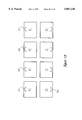
- FIG. 2 shows a top view of a 2 ⁇ 2 tiled, flat-panel display 19;
- FIG. 3 shows the side view thereof.
- Each tile 1-1, 1-2, 2-1 and 2-2, shown in FIGS. 2 and 3, is similar in cross-section to the monolithic display or tile 10 shown in FIG. 1.
- a cover plate 20 and a backplate 22 enclose the upper and lower surfaces, respectively, of a plurality of tiles 10.
- the construction, design, manufacture and function of tiled, flat-panel displays are described in detail in U.S. patent application Ser. Nos. 08/593,759 and 08/571,208, filed on Jan. 29, 1996, and Dec. 12, 1995, respectively, and are hereby incorporated by reference.
- the maximum number of tiles in an array of tiles is not limited, but arrays greater than 2 ⁇ 2 may require different sealing and assembly approaches than some of those suitable for a 2 ⁇ 2 array.
- This disclosure is not limited to arrays having the same number of tiles in a row as in a column.
- FIG. 4 shows a 3 ⁇ 4 array 24 of tiles, for which the present invention applies.
- FIG. 5 shows the 2 ⁇ 2 array of tiles 19 with the locations of wide seal bands 28 and narrow seal bands 26 illustrated.
- Tile edges at the overall display perimeter can be wide, while interior seals are narrow.
- a narrow seal 26 (in the range of 25-to-125 microns or larger) may be fabricated by using a MICRO PENTM-type tool, not shown, described in greater detail in U.S. patent application Ser. No. 08/571,208, filed Dec. 12, 1995, hereby incorporated by reference.
- An alternative type of narrow seal 26, also described in U.S. patent application Ser. No. 08/571,208 may be fabricated by screening a wide seal in the range of 100 microns or wider, using conventional screening technology on the top plates 12 and/or lower plates 14 of the AMLCD tiles.
- AMLCDs have wider seals 28 at all four edges of the display, which are useful to leave in place at non-abutting tile edges.
- a robust, additional, outer seal may be constructed to enclose the mosaic of tiles.
- hermetic and/or semi-hermetic, inner seals can be designed that employ minimum seal dimensions, which may or may not require an outer seal.
- the first, preferred approach is to enclose the tiles 10 within glass plates: a backplate 22 (FIG. 3) (which may or may not contain interconnection) and a cover plate 20 (which may contain a mask and additional optical function, e.g., a polarizer, not shown).
- the tiles 10 are, preferably, mechanically bonded both to the cover plate 20 and the backplate 22 with robust, adhesive seals (i.e., in the range of several millimeters in width), not shown here.
- both the cover plate 20 and the backplate 22 have equal thermal expansion coefficients (CTEs), which are also equal to those of the AMLCD tiles 10.
- CTEs thermal expansion coefficients
- these enclosing glass plates 20 and 22 should have optical properties that are similar to the glass of the AMLCD tiles 10.
- the most practical approach currently is to use the identical glass used for the tiles 10 (commonly, Corning 1737 glass), but with a thickness of 1.1 millimeters for robustness.
- the lot-to-lot glass composition variance is generally less than one percent. Since the thermal expansion coefficient is an intrinsic property, the two opposing glass plates 20 and 22 will have only a small variance in CTE (also in the range of one percent), depending on their composition.
- the thermal strains in the adhesive joints in the glass stack (20, 12, 14 and 22) are generally accepted to be proportional to the difference in the CTE of the glass, proportional to the temperature difference between the glass plates, inversely proportional to the thickness of the adhesive, and proportional to the distance between the mechanical neutral point of the design and the adhesive joint.
- the inventive design is mechanically robust, due to the selection of the particular design elements and their symmetrical organization in the glass stack.
- Adhesion of polymers to glass is often enhanced by chemical and/or mechanical treatments or combinations thereof to the glass surface.
- the glass may be micro-roughened by chemical etchant, for example, mixtures of ammonium fluoride, hydrofluoric acid and acetic acid. With this treatment and variables of time and temperature, a broad range of surface roughness may be accomplished.
- Polarized polymeric chemicals like AIP-10, A 1100, or a broad range of silicones provide chemical bonding at glass interfaces, preventing deleterious effects from moisture and enhancing mechanical strength.
- Combinations of the treatments are particularly effective in preventing shear stress crack growth at the interface between polymers and planar glass surfaces.
- a polymide coating is used to interface to the liquid crystal. This part of the process is classed as critical since it depends on the cure state of the polymide and a final "rubbing", which apparently orients the polymide molecules sufficiently to create a cooperative effect in the liquid crystal.
- the polymide area extends to the seal area and may, for narrow seals, cover the glass area to be sealed.
- the treatments noted above are generally sufficient to provide adequate adhesion between polymide and glass.
- the adhesion between the polymeric seal material and the polymide is dependent on interdiffusion of the polymer (generally epoxy) and the polymide--the interdiffusion is dependent on the cure state of the polymide.
- seal material for example, epoxy
- interdiffusion or chemical bonding may be substantial enough to provide adequate adhesion between the epoxy seal material and the polymide to allow the tiles to be cut without damage.
- secondary seal means along the edges of the tiles may be applied so that the tile withstands further processing and handling--adequate support of top and bottom plates of the tile during cutting (FIG. 5a) may be essential.
- an outer seal 28' outside the inner, narrow seal 26 by slightly more than a sawblade width provides the desired support.
- An alternative to sealing the tiles on a polymide interface is to remove the polymide, leaving either a clean glass interface or one optimized for adhesion and mechanical integrity as described previously.
- the polymide may be removed locally in the narrow seal area.
- a practical approach is to plasma etch the material selectively using the same mask as that used to screen the adhesive.
- the chosen technique must be compatible with the "rubbed" polymide surface retaining its cooperative interaction for orienting the liquid crystal.
- Lift-off masking techniques may be used to remove unwanted polyimide.
- masking followed by etching e.g., KOH solution, may be used.
- the backplate 22 of the AMLCD tiles 10 extends beyond the top plate 12 of the tiles 10 and beyond the cover plate 20.
- the interconnection for the AMLCD electronics extends a predetermined distance on the lower plate 14, for easy access to wire, TAB or other interconnections, which connect to PCB electronics surrounding the FPD.
- Seals 28 on the top and left sides of tile 1-1 can be relatively wide because they are outside the display's pixel field. Seals 26 on the bottom and right sides of the tile 1-1 are preferably narrow, so as to accommodate the pixel pitch with a desirable aperture efficiency throughout the display. Sealing of the cover plate 20 to the top plate 12 of the tile 1-1 is accomplished as decribed hereinbelow.
- FIGS. 6 and 7 show the location of electrical connections 30 to the array 19. Sealing integrity should be maintained while making these connections.
- FIGS. 8 and 9 show a preferred approach to solving both the mechanical and environmental problems of sealing.
- Tiles 10, the edges of which have narrow seals 26, are enclosed with the glass cover plate 20 and the backplate 22.
- These plates 20 and 22 are adhesive-bonded by robust seals 32 and 34, respectively, to the tiles 10 on the outside perimeter of the tiled display. Since they are outside the viewing area, there is a liberal design freedom associated with the width, thickness and mechanical strength of the seals 32 and 34.
- the glass enclosure (plates 20 and 22) is preferably matched in thermal expansion to the AMLCD tiles 10 (FIG. 1).
- the vertical seams 36 are sealed on the outside perimeter with a small amount of polymer 36a, which may be dispensed with a dropper, syringe or other suitable means.
- the AMLCD tile's lower plate ledge 38 which contains the monolithic interconnection emerging from the seal, is left open for bonding to the drivers and control circuits, not shown, outside of the tiled, FPD area.
- the interconnections 30 can thus be made as if the FPD were monolithic.
- FIG. 10 shows an alternative structure having the tile's entire top face of the top plate 12 and bottom face of the lower plate 14 adhesive-sealed 40 to the FPD coverplate 20 and backplate 22.
- FIG. 11 shows a 2 ⁇ 4 array 42 of tiles 10. It can be seen that individual tiles 10 have either two or three edges with narrow seals 26. In FIG. 12, showing a 3 ⁇ 3 tile array 44, two or more of the edges of each tile have narrow seals 26.
- the sealing concepts shown in FIGS. 8, 9 and 10 can also be used with these designs.
- a backplate with interconnections or multilevel interconnections is needed.
- the tiles may be interconnected to the backplate with TABs, wire bonds or alternatives.
- FIG. 13 shows a preferred, alternative sealing concept, in which the backplate 22 may be circuitized with thin films for a 2 ⁇ N array. Electrical connections 30 are made between the tiles 10 and the backplate 22 when the backplate is circuitized.
- the composite seal 44 may be constructed between the backplate 22 and the cover plate 20.
- the height 46 of the composite seal 44 is approximately equal to the thickness of the two glass plates 12 and 14 making up the AMLCD tile 10, plus any spacing between the AMLCD tile 10 and the backplate 22 and between the AMLCD tile 10 and the cover plate 20.
- This additional space may contain interconnections, one or more polarizers and a mask, not shown, as well as adhesive with spacers to establish coplanarity within the tiles and the cover plate.
- the total space to seal will be larger than 1.4 millimeters.
- the composite seal 44 consisting of a combination of non-permeable material 48 filling the space, along with conventional polymeric seals 50 and 50', which provide adequate environmental protection.
- glass or alternative spacers are bonded between the cover plate 20 and the backplate 22 with polymeric seal materials.
- Seal widths may be in the range of several millimeters, while the polymeric seal adhesive may be in the thickness range of several microns (similar to the seals used for monolithic FPDs).
- electrical feed-throughs may be contained in the non-permeable seal, with external and internal connections to the feed-throughs.
- FIG. 13a shows an alternative sealing concept, in which an end cap 48' surrounds the display at the perimeter and is sealed 50" to the cover plate 20 and the backplate 22. Electrical feed-through connections 30' penetrate and are sealed in the end cap 48'.
- the first design embodiment applies to 2 ⁇ 2 tile array designs (e.g., 19 in FIGS. 2 and 6) and incorporates a strip of thin metal film 52, which is adhesive-bonded to the two edges 54 and 56 of the tile 10 shown in FIG. 14.
- the strip of metal film 52 may be continuous around the corner 58, or may be two separate pieces, as shown.
- the adhesive in this case may be substantially thinner than the conventional, 5-micron seal used in AMLCDs.
- the strip of metal film 52 is impermeable; therefore, the diffusion path is through the thin adhesive for a distance that is equal to the thickness of the glass 12 or 14 (typically, 0.7 millimeters), then through the 5-micron seal 26 of the tile 10 to the liquid-crystal material 18.
- This technique has a diffusion length comparable to a conventional AMLCD and is, therefore, expected to provide adequate semi-hermetic performance.
- the mechanical robustness is determined by the thickness and the strength of the strip of metal film 52, and is expected to result in one or two orders of magnitude of greater strength than the epoxy polymers that are currently used for sealing.
- a second embodiment eliminating the need for an outer seal and a backplate consists of coating the AMLCD edges with material made of ParyleneTM, or other materials such as liquid-crystal polymer, having an exceptionally low permeability and/or solubility for water.
- ParyleneTM material can be deposited by sublimination, forming a conformal coating with essentially equal thickness on edges 54 and 56, corners 58 and crevices, as well. This ParyleneTM can be used in conjunction with the narrow seals 26 between the plates 12 and 14.
- FIG. 15 shows the edges of an individual tile 10 before coating. All four edges may, of course, be coated; the entire tile 10 may even be coated, if the necessary steps are taken to maintain optical transparency and electrical connection integrity.
- One preferred seal material is a Solgel glass composition 60 which sinters in the temperature range below the recrystallization temperature of amorphous silicon.
- Silica Solgel materials 60 sinter in the range of 300° C. to 400° C., a temperature which is acceptable for polysilicon AMLCD; this is an emerging technology.
- temperatures in the range of 300° C. to 400° C. could cause the amorphous silicon that is used for the transistor in current AMLCD technology to recrystallize.
- Lower sintering temperatures for Solgel may be achieved by using glass compositions containing lead and other elements. With the desired elements in the glass, it may be feasible to sinter the Solgel at temperatures which the amorphous silicon can withstand.
- the Solgel seals 60 are deposited with a MICRO PENTM in the same way as are narrow polymer seals. Spherical glass spacers or alternatives of desired diameter, are preferably mixed with the Solgel to control the spacing between the top and bottom plates of the tile. A vacuum bake sinters the seal in place. Localized heating (e.g., by laser) can be used to repair the sintered Solgel seals.
- Glass seals 60 produced in the manner discussed have several advantages. First, the glass seal prevents the diffusion of moisture. Secondly, the strength of the material and the bonding provides increased mechanical reliability. Finally, as the processing is learned, seals may be constructed that are as narrow as can be effectively deposited (e.g., in the range of one-thousandth of an inch wide). The Solgel seal approach is adaptable to all edges of the tiles 10, including those that contain interconnections.
- a fourth embodiment of a seal for application to 1 ⁇ 2 or 2 ⁇ 2 AMLCD tile arrays uses an SnPb, an SnBi or an alternative solder with melting temperatures in the desired range.
- a sputtered or evaporated thin metal film (such as chromium) is used as the adhesive element for the glass; a copper film is superimposed to form a wettable interface that is adaptable for soldering.
- a convenient processing configuration is a set of AMLCD tiles stacked on edge. The metal film is sputtered on the edges of both the top plate 12 and lower plate 14 of multiple tiles concurrently. This is followed by a solder application to the metallized edges, bridging the 5-micron gap between the lower plate 14 and the top plate 12. Solder can be applied by many methods well known in the art.
- solder bridges the 5-micron gap between the lower 14 and top plates 12 of a tile 10 with a truly hermetic seal. Furthermore, on cooling, the solder creates a compressive stress on the two plates, holding them in place in spite of substantial shear or tensile forces.
- optical matching at the interfaces is desirable and may be accomplished (at least, partly) by selecting suitable AMLCD tiles. If the matching from tile to tile is not adequate, electronic trimming of the individual, color light-valves, as described in copending U.S. Pat. No. 5,661,531, may be desirable.
- FIG. 17 shows examples of the location of ports for a 2 ⁇ 2 array of tiles.
- FIG. 18 shows port locations for 2 ⁇ M, where M is an integer greater than 2.
- Liquid-crystal material 18 is flooded into the space between the top 12 and lower plates 14 of a tile 10 by immersing the structure in a bath of liquid-crystal material 18 in a vacuum environment. The liquid-crystal material 18 enters the space between the glass plates 12 and 14 through "ports" 62 in the seal. Where two tiles are adjacent at a seam, the optical response of the neighboring areas, tile to tile, should be as close to identical as possible.
- the locations of fill ports 62 are situated so as to ensure that the liquid-crystal material 18 flows in a symmetrical pattern with respect to the pattern of adjacent tiles 10 in the array, thus promoting improved optical uniformity.
- Optical discontinuity may be minimized by maintaining the fill ports 62 on the edges of the tiles 10 in a symmetrical arrangement, with respect to the perimeter of the FPD.
- polarizers 64 and 64' are adhesive-bonded to the top 12 and lower plates 14, respectively, of each tile 10.
- a continuous adhesive 66 bonds the tiles 10 with polarizers 64 to the cover plate/mask assembly 20 and 68.
- a film, not shown, which may be removed by peeling prior to bonding, may be used to protect the adhesive 66.
- the sealing method shown in FIGS. 8 and 9 may be used.
- the top surfaces of the tiles 10 with polarizers 64 attached may be registered and bonded to the cover plate/mask assembly, 20 and 68. This assembly sequence maximizes co-planarity at the viewing surface.
- TABs, wires or other connecting means 30 are preferably attached to pads, not shown, on the tiles 10, before the tiles 10 are bonded to the cover plate 20.
- the tiles 10 may then be functionally tested prior to being committed to assembly.
- Tiles can be characterized as "Known Good Tiles” (KGT), which is similar to the concept of "Known Good Die” (KGD) in the assembly of multi-chip modules in the electronics industry.
- FIG. 20 shows a single tile 10 with column driver--and row driver TABs 74 and 76, respectively, attached for KGT characterization.
- a multi-tile assembly may also be tested prior to its attachment to the backplate (if used), and prior to any further assembly.
- compliant spacers 72a are used underneath the tiles. These are contained in sufficient proportion in the adhesive 72 and 72', supporting the individual tiles 10 until an additional pressure is applied.
- the size of the polymer spacers is designed to be greater than the maximum tolerance accumulation difference for the tiles in the array.
- 2 ⁇ N arrays In the case of 2 ⁇ N arrays, a sequence is preferred in which the tiles are assembled to the backplate first, but are made co-planar to the cover plate.
- the steps to manufacture 2 ⁇ N arrays include:
- row drivers and column drivers may drive lines across the total length and width of the AMLCD.
- a choice may be made as to whether to provide jumper interconnection means (such as from tile 1-1 to tile 1-2 for row lines), or provide drivers for each tile along the peripheral edges, as shown in FIG. 21.
- driver lines 77 for interior tiles of arrays greater than 2 ⁇ 2 are provided on the backplate 22, so as not to disturb optical transmission.
- tiles 1-2 and 2-2 have driver lines external to the tiles, e.g., on the top surface of the backplate.
- These row driver lines 76 may be shared with other tiles (e.g., 1-1, 1-1 and 2-1, 2-2), or they may be dedicated to the inner tiles (e.g., 1-2, 2-2). If drivers are shared, means may be provided to connect each tile to the appropriate line on the backplate.
- the drivers for tiles 1-1, 2-1, 1-3 and 2-3 are not shown in FIG. 23.
- Similar arrangements may be employed for either row driver lines 76 or column driver lines, not shown in FIG. 23, or both.
- Arrays greater than 2 ⁇ 2 in each direction may have driver lines in a two-layer interconnection structure on the backplate, or with one layer provided on the backplate and another on a separate means interposed between the backplate and the tiles.
- tile-to-tile jumpers may eliminate the need for backplate circuitization in either or both directions.
- FIG. 24 shows the connection design for providing row driver inputs to the inner tiles of the array shown in FIG. 22.
- Column driver inputs for the inner tiles may be provided at the display perimeter, but row driver inputs (having passed under tiles 1-1 and 2-1 on the backplate 22) must be connected to the pads 78 on the lower plates 14 of tiles 1-2 and 2-2.
- These pads 78 are located on a narrow (approximately 0.1 mm) ledge 38 of the tile. Since only one line per pixel is required for row drivers, the pitch of these pads 78 may be a significant percentage of the pixel pitch.
- the pixel pitch may be greater than a few tenths of a millimeter.
- Reliable connections, using an isotropic conductive adhesive 80 require multiple points of contact at each pad 78.
- Feasible ledge dimensions allow the use of TABS with widths approaching a full pixel pitch for isotropic conductive interconnects 80. This fulfills the multiple contact requirement for an isotropic adhesive 80 on the ledges 38 of tiled displays.
- Such connections may be made between the flex 82 and the backplate 22, and between the flex 82 and the pad 78 on the tile's lower plate 14.
- Other connection technologies such as thermo-compression bonding (TCB) or soldering, may also be employed.
- the flex connection 82 to the backplate 22 may be outside the shadow of the tile 10, as shown in FIG. 25, or folded under the tile 10, so as to minimize the dimension which must be accommodated in the seamless design.
- FIG. 25 shows a connection diagram at a pixel element for row and column drivers on a common tile edge.
- Column driver lines 83 between columns of sub-pixels 84 deliver column inputs to TFT transistors 85 to control voltage levels at electrodes of the sub-pixels.
- C com lines 86 and row driver lines 87 (similar in concept, but differing in location to row driver lines 77 shown in FIG. 23), may be routed between pixels in a direction parallel to column driver lines 83.
- Row driver lines 87 may be routed on a second wiring plane, not shown, to deliver row driver inputs to TFT transistors 85.
- C com lines 86 may be routed on this second wiring plane to provide connections to capacitors 89.
- FIG. 26 shows this connection concept for a tiled array of pixels.
- multiple row (gate) lines 87 may be routed between pixels to provide row drivers for tile arrays with a larger number of rows than columns.
Abstract
Description
Claims (22)
Priority Applications (2)
| Application Number | Priority Date | Filing Date | Title |
|---|---|---|---|
| US08/652,032 US5867236A (en) | 1996-05-21 | 1996-05-21 | Construction and sealing of tiled, flat-panel displays |
| US09/136,693 US6639643B2 (en) | 1996-05-21 | 1998-08-19 | Method of constructing and sealing tiled, flat-panel displays |
Applications Claiming Priority (1)
| Application Number | Priority Date | Filing Date | Title |
|---|---|---|---|
| US08/652,032 US5867236A (en) | 1996-05-21 | 1996-05-21 | Construction and sealing of tiled, flat-panel displays |
Related Child Applications (1)
| Application Number | Title | Priority Date | Filing Date |
|---|---|---|---|
| US09/136,693 Division US6639643B2 (en) | 1996-05-21 | 1998-08-19 | Method of constructing and sealing tiled, flat-panel displays |
Publications (1)
| Publication Number | Publication Date |
|---|---|
| US5867236A true US5867236A (en) | 1999-02-02 |
Family
ID=24615248
Family Applications (2)
| Application Number | Title | Priority Date | Filing Date |
|---|---|---|---|
| US08/652,032 Expired - Lifetime US5867236A (en) | 1996-05-21 | 1996-05-21 | Construction and sealing of tiled, flat-panel displays |
| US09/136,693 Expired - Fee Related US6639643B2 (en) | 1996-05-21 | 1998-08-19 | Method of constructing and sealing tiled, flat-panel displays |
Family Applications After (1)
| Application Number | Title | Priority Date | Filing Date |
|---|---|---|---|
| US09/136,693 Expired - Fee Related US6639643B2 (en) | 1996-05-21 | 1998-08-19 | Method of constructing and sealing tiled, flat-panel displays |
Country Status (1)
| Country | Link |
|---|---|
| US (2) | US5867236A (en) |
Cited By (83)
| Publication number | Priority date | Publication date | Assignee | Title |
|---|---|---|---|---|
| US6005649A (en) * | 1998-07-22 | 1999-12-21 | Rainbow Displays, Inc. | Tiled, flat-panel microdisplay array having visually imperceptible seams |
| US6097455A (en) * | 1999-05-28 | 2000-08-01 | Rainbow Displays Inc. | Flat panel displays having tiles and visually imperceptible gaps therebetween |
| US6100584A (en) * | 1997-03-31 | 2000-08-08 | Sanyo Electric Co., Ltd. | Glass board used in the production of liquid crystal panels |
| US6115092A (en) * | 1999-09-15 | 2000-09-05 | Rainbow Displays, Inc. | Compensation for edge effects and cell gap variation in tiled flat-panel, liquid crystal displays |
| US6129804A (en) * | 1998-05-01 | 2000-10-10 | International Business Machines Corporation | TFT panel alignment and attachment method and apparatus |
| US6144438A (en) * | 1995-10-11 | 2000-11-07 | Sharp Kabushiki Kaisha | Liquid crystal display device of multi-panel type and method for fabricating the same |
| WO2001011420A1 (en) * | 1999-08-06 | 2001-02-15 | Rainbow Displays, Inc. | Design features optimized for tiled flat-panel displays |
| WO2001011421A1 (en) * | 1999-08-06 | 2001-02-15 | Rainbow Displays, Inc. | Design features optimized for tiled flat-panel displays |
| US6193576B1 (en) * | 1998-05-19 | 2001-02-27 | International Business Machines Corporation | TFT panel alignment and attachment method and apparatus |
| US6249329B1 (en) * | 1996-06-13 | 2001-06-19 | Rainbow Displays, Inc. | Assembling and sealing large, hermetic and semi-hermetic H-tile flat panel display |
| WO2001054106A2 (en) * | 2000-01-24 | 2001-07-26 | Rainbow Displays, Inc. | A tiled flat-panel display having visually imperceptible seams, optimized for hdtv applications |
| WO2001053883A1 (en) * | 2000-01-21 | 2001-07-26 | Rainbow Displays, Inc. | Construction of large, robust, monolithic and monolithic-like, amlcd displays with wide view angle |
| EP1130567A2 (en) * | 2000-02-24 | 2001-09-05 | AEG Gesellschaft für moderne Informationssysteme mbH | Pixel element for a LCD matrix, graphical LCD display comprising a plurality of these pixel elements and method of controlling the luminance of the pixel element respectively the display matrix |
| US6317186B1 (en) * | 1998-12-28 | 2001-11-13 | International Business Machines Corporation | Method for sealing corner regions of a liquid crystal display |
| US6341879B1 (en) * | 1999-09-28 | 2002-01-29 | Rainbow Displays, Inc. | High output flat-panel display back light module |
| WO2002019017A1 (en) * | 2000-08-28 | 2002-03-07 | Rainbow Displays, Inc. | Construction of large, robust, monolithic and monolithic-like, amlcd displays with wide view angle |
| US6370019B1 (en) | 1998-02-17 | 2002-04-09 | Sarnoff Corporation | Sealing of large area display structures |
| WO2002050605A1 (en) * | 2000-12-20 | 2002-06-27 | Koninklijke Philips Electronics N.V. | Active matrix device |
| US6417832B1 (en) | 1999-09-28 | 2002-07-09 | Rainbow Displays, Inc. | Apparatus for producing uniform luminance in a flat-panel display backlight |
| US6476783B2 (en) | 1998-02-17 | 2002-11-05 | Sarnoff Corporation | Contrast enhancement for an electronic display device by using a black matrix and lens array on outer surface of display |
| US6476886B2 (en) * | 1999-02-15 | 2002-11-05 | Rainbow Displays, Inc. | Method for assembling a tiled, flat-panel microdisplay array |
| US20020168157A1 (en) * | 2000-12-14 | 2002-11-14 | Walker James K. | Method and apparatus for fabrication of plastic fiber optic block materials and large flat panel displays |
| US6491560B1 (en) | 2000-05-25 | 2002-12-10 | Motorola, Inc. | Array tile system and method of making same |
| US6498592B1 (en) | 1999-02-16 | 2002-12-24 | Sarnoff Corp. | Display tile structure using organic light emitting materials |
| US20030001999A1 (en) * | 2001-06-14 | 2003-01-02 | Kim Jin Mahn | Sealing structure and sealing method of liquid crystal display |
| US20030011724A1 (en) * | 2001-07-16 | 2003-01-16 | Sundahl Robert C. | Repairable tiled displays |
| US20030011303A1 (en) * | 2001-07-12 | 2003-01-16 | Matthies Dennis L. | Providing optical elements over emissive displays |
| US6556261B1 (en) * | 1999-02-15 | 2003-04-29 | Rainbow Displays, Inc. | Method for assembling a tiled, flat-panel microdisplay array having reflective microdisplay tiles and attaching thermally-conductive substrate |
| US20030090198A1 (en) * | 2001-11-10 | 2003-05-15 | Mark Aston | Display |
| US6573957B1 (en) * | 1999-08-18 | 2003-06-03 | International Business Machines Corporation | Liquid crystal display device |
| US6602762B2 (en) * | 2001-07-05 | 2003-08-05 | Chipbond Technology Corporation | System and method of laser sintering dies and dies sintered by laser sintering |
| US6624570B1 (en) * | 1999-09-29 | 2003-09-23 | Sanyo Electric Co., Ltd. | Electroluminescent display device and method for its fabrication |
| US20030184703A1 (en) * | 2000-01-21 | 2003-10-02 | Greene Raymond G. | Construction of large, robust, monolithic and monolithic-like, AMLCD displays with wide view angle |
| US20030214237A1 (en) * | 1999-08-06 | 2003-11-20 | Samsung Sdi Co., Ltd. | Method of fabricating plasma display panel |
| US6667783B2 (en) * | 2000-01-21 | 2003-12-23 | Rainbow Displays, Inc. | Construction of large, robust, monolithic and monolithic-like, AMLCD displays with wide view angle |
| US6683665B1 (en) | 2000-11-20 | 2004-01-27 | Sarnoff Corporation | Tiled electronic display structure and method for modular repair thereof |
| US20040051451A1 (en) * | 2002-09-13 | 2004-03-18 | Kimitaka Kawase | Display unit |
| US6753096B2 (en) | 2001-11-27 | 2004-06-22 | General Electric Company | Environmentally-stable organic electroluminescent fibers |
| US20040168758A1 (en) * | 2003-02-28 | 2004-09-02 | Kabushiki Kaisha Topcon | Optical member and method of producing the same |
| US6795153B2 (en) | 2001-04-18 | 2004-09-21 | International Business Machines Corporation | Display panel, laminated substrate, liquid crystal cell and method of manufacturing laminated substrate |
| US6822389B2 (en) * | 2001-10-11 | 2004-11-23 | Intel Corporation | Array display including resilient material in the seam |
| US20040256977A1 (en) * | 2001-11-10 | 2004-12-23 | Mark Aston | Overlapping array display |
| US20050078104A1 (en) * | 1998-02-17 | 2005-04-14 | Matthies Dennis Lee | Tiled electronic display structure |
| US20050093768A1 (en) * | 2003-10-31 | 2005-05-05 | Devos John A. | Display with interlockable display modules |
| US6980272B1 (en) | 2000-11-21 | 2005-12-27 | Sarnoff Corporation | Electrode structure which supports self alignment of liquid deposition of materials |
| US20060108915A1 (en) * | 2004-11-23 | 2006-05-25 | Eastman Kodak Company | Tiled OLED display |
| US20060181666A1 (en) * | 2001-08-21 | 2006-08-17 | Jong-Chil Lee | Seal pattern for liquid crystal display device |
| US20070001927A1 (en) * | 2005-07-01 | 2007-01-04 | Eastman Kodak Company | Tiled display for electronic signage |
| KR100720425B1 (en) | 2002-12-24 | 2007-05-22 | 엘지.필립스 엘시디 주식회사 | Liquid Crystal Display device |
| US20070290614A1 (en) * | 2003-08-22 | 2007-12-20 | 3M Innovative Properties Company | Electroluminescent devices and methods |
| USRE40355E1 (en) | 2001-07-18 | 2008-06-03 | Seiko Epson Corporation | Back light assembly for use with back-to-back flat-panel displays |
| US20090147177A1 (en) * | 2007-12-06 | 2009-06-11 | Samsung Mobile Display Co., Ltd. | Multi-vision display |
| US20090312884A1 (en) * | 2008-06-13 | 2009-12-17 | Li zheng min | Method for power sharing and controlling the status of a display wall |
| US20100156779A1 (en) * | 2008-12-22 | 2010-06-24 | Park Sung-Jin | Electrophoretic display device and method of fabricating the same |
| EP2189970A3 (en) * | 2003-12-04 | 2010-09-15 | Shearline Precision Engineering Limited | Display |
| US20120287021A1 (en) * | 2009-12-11 | 2012-11-15 | Tovis Co., Ltd. | Display device for connecting plurality of lcd panels |
| US20140218918A1 (en) * | 2011-05-16 | 2014-08-07 | Sharp Kabushiki Kaisha | Multi display system, and display device |
| US20150084024A1 (en) * | 2013-09-24 | 2015-03-26 | Gentex Corporation | Glass strip as a seal |
| US9013102B1 (en) | 2009-05-23 | 2015-04-21 | Imaging Systems Technology, Inc. | Radiation detector with tiled substrates |
| US20150277173A1 (en) * | 2014-03-26 | 2015-10-01 | Samsung Electronics Co., Ltd. | Tiled display and bezelless liquid crystal display apparatus |
| KR20150111808A (en) * | 2014-03-26 | 2015-10-06 | 삼성전자주식회사 | Tiled display, and Bezelless liuid crystal display apparatus |
| WO2015198803A1 (en) * | 2014-06-25 | 2015-12-30 | ソニー株式会社 | Display device |
| US20160154262A1 (en) * | 2014-11-27 | 2016-06-02 | Samsung Display Co., Ltd. | Tiled display device |
| US9529563B2 (en) * | 2014-09-30 | 2016-12-27 | X Development Llc | Masking mechanical separations between tiled display panels |
| US20170082890A1 (en) * | 2015-09-22 | 2017-03-23 | Samsung Display Co., Ltd. | Display device |
| US20170307922A1 (en) * | 2014-09-15 | 2017-10-26 | Barco N.V. | Display tile with increased display area |
| US9887215B2 (en) * | 2014-08-22 | 2018-02-06 | Au Optronics Corporation | Display module manufacturing method and display module |
| US20180130425A1 (en) * | 2016-11-09 | 2018-05-10 | Lg Electronics Inc. | Display apparatus |
| US20180180937A1 (en) * | 2016-06-14 | 2018-06-28 | Shenzhen China Star Optoelectronics Technology Co. Ltd. | Transparent liquid crystal display |
| WO2018205475A1 (en) * | 2017-05-10 | 2018-11-15 | 西安诺瓦电子科技有限公司 | Spliced display screen configuration method and device, and display screen control card |
| GB2567649A (en) * | 2017-10-18 | 2019-04-24 | Motionled Tech Limited | Display panel |
| US20190334113A1 (en) * | 2018-04-27 | 2019-10-31 | Wuhan China Star Optoelectronics Technology Co., Ltd. | Oled display device |
| USD895160S1 (en) * | 2019-01-10 | 2020-09-01 | Unmatched Bonding Company LLC | Industrial tile |
| US11011084B1 (en) * | 2020-02-04 | 2021-05-18 | Christie Digital Systems Usa, Inc. | Modular mounting system |
| US11191178B2 (en) | 2019-01-24 | 2021-11-30 | Steelcase Inc. | Display support system and method for the use thereof |
| CN113782556A (en) * | 2021-09-10 | 2021-12-10 | 深圳市华星光电半导体显示技术有限公司 | Display panel manufacturing method, spliced screen manufacturing method and display device |
| USD941503S1 (en) | 2020-08-25 | 2022-01-18 | Unmatched Bonding Limited | Abrasion-resistant cuttable self-adhesive industrial tile |
| USD941504S1 (en) | 2020-08-25 | 2022-01-18 | Unmatched Bonding Limited | Abrasion-resistant cuttable self-adhesive industrial tile |
| USD941505S1 (en) | 2020-08-25 | 2022-01-18 | Unmatched Bonding Limited | Abrasion-resistant cuttable self-adhesive industrial tile |
| US20220059644A1 (en) * | 2020-08-19 | 2022-02-24 | Lg Display Co., Ltd. | Tiling Display Device |
| US11269208B2 (en) * | 2019-09-11 | 2022-03-08 | Samsung Display Co., Ltd. | Display device comprising a first auxiliary substrate including a first section and a second section oriented at a first right-or-acute angle relative to the first section and tiled display apparatus including the same |
| CN115472095A (en) * | 2022-08-25 | 2022-12-13 | 惠科股份有限公司 | Display device and method for manufacturing the same |
| US11647834B2 (en) | 2020-07-23 | 2023-05-16 | Steelcase Inc. | Display support system and method for the use thereof |
Families Citing this family (22)
| Publication number | Priority date | Publication date | Assignee | Title |
|---|---|---|---|---|
| US6204906B1 (en) * | 1999-03-22 | 2001-03-20 | Lawrence E. Tannas, Jr. | Methods of customizing the physical size and shape of commercial off-the-shelf (COTS) electronic displays |
| US7081928B2 (en) * | 2001-05-16 | 2006-07-25 | Hewlett-Packard Development Company, L.P. | Optical system for full color, video projector using single light valve with plural sub-pixel reflectors |
| JP3838964B2 (en) | 2002-03-13 | 2006-10-25 | 株式会社リコー | Functional element substrate manufacturing equipment |
| JP2005524110A (en) * | 2002-04-24 | 2005-08-11 | イー−インク コーポレイション | Electronic display device |
| GB0216904D0 (en) * | 2002-07-20 | 2002-08-28 | Koninkl Philips Electronics Nv | Active matrix liquid crystal display device |
| ATE314679T1 (en) * | 2002-11-14 | 2006-01-15 | Mitron Oy | METHOD FOR PRODUCING AN INFORMATION DISPLAY AND AN INFORMATION DISPLAY |
| KR20040048617A (en) * | 2002-12-04 | 2004-06-10 | 오리온전기 주식회사 | Method for fabricating multi-PDP |
| TW586329B (en) * | 2003-01-29 | 2004-05-01 | Au Optronics Corp | Sealing structure and method of making the same |
| JP4059153B2 (en) * | 2003-06-23 | 2008-03-12 | ソニー株式会社 | Manufacturing method of display device |
| US7667815B2 (en) * | 2003-08-27 | 2010-02-23 | Ming Su | Multi-panel monitor displaying systems |
| US7344671B2 (en) * | 2003-11-26 | 2008-03-18 | Glopak Inc. | Optical sealing clamp and a method for sealing and cutting polymeric sheets with a laser |
| US20060077126A1 (en) * | 2004-09-27 | 2006-04-13 | Manish Kothari | Apparatus and method for arranging devices into an interconnected array |
| US20060256267A1 (en) * | 2005-05-10 | 2006-11-16 | Bone Matthew F | Method for manufacturing liquid crystal display devices and devices manufactured thereby |
| US20080168801A1 (en) * | 2007-01-12 | 2008-07-17 | Paul Stephen Danielson | Method of sealing glass |
| WO2009099425A2 (en) | 2008-02-07 | 2009-08-13 | Qd Vision, Inc. | Flexible devices including semiconductor nanocrystals, arrays, and methods |
| RU2542963C2 (en) * | 2008-09-05 | 2015-02-27 | Селджен Авиломикс Рисерч,Инк., | Method of determining inhibitor, covalently binding target polypeptide |
| US8854576B2 (en) * | 2011-10-21 | 2014-10-07 | Corning Incorporated | Semitransparent electronic device |
| US9025111B2 (en) | 2012-04-20 | 2015-05-05 | Google Inc. | Seamless display panel using fiber optic carpet |
| US11119616B2 (en) | 2018-11-01 | 2021-09-14 | Apple Inc. | Trace transfer techniques for touch sensor panels with flex circuits |
| US11853515B2 (en) | 2018-12-19 | 2023-12-26 | Apple Inc. | Ultra-thin touch sensors |
| KR102599722B1 (en) * | 2018-12-28 | 2023-11-09 | 삼성디스플레이 주식회사 | Display panel ad tiled display apparatus having the same |
| CN114303184A (en) * | 2019-08-30 | 2022-04-08 | 华为技术有限公司 | Display screen and terminal equipment |
Citations (8)
| Publication number | Priority date | Publication date | Assignee | Title |
|---|---|---|---|---|
| US3932024A (en) * | 1971-08-18 | 1976-01-13 | Dai Nippon Toryo Kabushiki Kaisha | Electro-optical devices |
| US3967882A (en) * | 1971-04-09 | 1976-07-06 | Kabushiki Kaisha Suwa Seikosha | Liquid crystal display device having extended service life |
| US4158485A (en) * | 1975-02-10 | 1979-06-19 | Siemens Aktiengesellschaft | Liquid crystal cell with a glass solder seal |
| US4466701A (en) * | 1981-08-25 | 1984-08-21 | Optrex Corporation | Highly reliable electrooptical device and process for manufacturing the same |
| US5106197A (en) * | 1989-12-22 | 1992-04-21 | Mitsubishi Denki Kabushiki Kaisha | Liquid crystal display apparatus |
| US5610742A (en) * | 1991-08-01 | 1997-03-11 | Seiko Epson Corporation | Liquid crystal display element, methods of producing and storing the same, and electronic equipment on which the same is mounted |
| US5654781A (en) * | 1994-12-15 | 1997-08-05 | Shart Kabushiki Kaisha | Liquid crystal display with electric wiring having an opening in an area where a seal member crosses |
| US5661531A (en) * | 1996-01-29 | 1997-08-26 | Rainbow Displays Inc. | Tiled, flat-panel display having invisible seams |
Family Cites Families (9)
| Publication number | Priority date | Publication date | Assignee | Title |
|---|---|---|---|---|
| US3861783A (en) * | 1973-06-28 | 1975-01-21 | Hughes Aircraft Co | Liquid crystal display featuring self-adjusting mosaic panel |
| JP3135793B2 (en) * | 1994-09-02 | 2001-02-19 | シャープ株式会社 | Liquid crystal display device and manufacturing method thereof |
| JP3131354B2 (en) * | 1994-09-02 | 2001-01-31 | シャープ株式会社 | Liquid crystal display |
| KR0139373B1 (en) * | 1994-10-06 | 1998-06-15 | 김광호 | Electrostatic shield circuit of lcd |
| JP3133228B2 (en) * | 1995-03-31 | 2001-02-05 | シャープ株式会社 | Display device |
| US5889568A (en) * | 1995-12-12 | 1999-03-30 | Rainbow Displays Inc. | Tiled flat panel displays |
| US5781258A (en) * | 1996-06-13 | 1998-07-14 | Rainbow Displays, Inc. | Assembling and sealing large, hermetic and semi-hermetic, h-tiled, flat-paneled displays |
| US5796452A (en) * | 1997-03-21 | 1998-08-18 | International Business Machines Corporation | Simplified wiring escape technique for tiled display |
| US5777705A (en) * | 1997-05-30 | 1998-07-07 | International Business Machines Corporation | Wire bond attachment of a liquid crystal display tile to a tile carrier |
-
1996
- 1996-05-21 US US08/652,032 patent/US5867236A/en not_active Expired - Lifetime
-
1998
- 1998-08-19 US US09/136,693 patent/US6639643B2/en not_active Expired - Fee Related
Patent Citations (8)
| Publication number | Priority date | Publication date | Assignee | Title |
|---|---|---|---|---|
| US3967882A (en) * | 1971-04-09 | 1976-07-06 | Kabushiki Kaisha Suwa Seikosha | Liquid crystal display device having extended service life |
| US3932024A (en) * | 1971-08-18 | 1976-01-13 | Dai Nippon Toryo Kabushiki Kaisha | Electro-optical devices |
| US4158485A (en) * | 1975-02-10 | 1979-06-19 | Siemens Aktiengesellschaft | Liquid crystal cell with a glass solder seal |
| US4466701A (en) * | 1981-08-25 | 1984-08-21 | Optrex Corporation | Highly reliable electrooptical device and process for manufacturing the same |
| US5106197A (en) * | 1989-12-22 | 1992-04-21 | Mitsubishi Denki Kabushiki Kaisha | Liquid crystal display apparatus |
| US5610742A (en) * | 1991-08-01 | 1997-03-11 | Seiko Epson Corporation | Liquid crystal display element, methods of producing and storing the same, and electronic equipment on which the same is mounted |
| US5654781A (en) * | 1994-12-15 | 1997-08-05 | Shart Kabushiki Kaisha | Liquid crystal display with electric wiring having an opening in an area where a seal member crosses |
| US5661531A (en) * | 1996-01-29 | 1997-08-26 | Rainbow Displays Inc. | Tiled, flat-panel display having invisible seams |
Cited By (148)
| Publication number | Priority date | Publication date | Assignee | Title |
|---|---|---|---|---|
| US6144438A (en) * | 1995-10-11 | 2000-11-07 | Sharp Kabushiki Kaisha | Liquid crystal display device of multi-panel type and method for fabricating the same |
| US6249329B1 (en) * | 1996-06-13 | 2001-06-19 | Rainbow Displays, Inc. | Assembling and sealing large, hermetic and semi-hermetic H-tile flat panel display |
| US6100584A (en) * | 1997-03-31 | 2000-08-08 | Sanyo Electric Co., Ltd. | Glass board used in the production of liquid crystal panels |
| US7864136B2 (en) | 1998-02-17 | 2011-01-04 | Dennis Lee Matthies | Tiled electronic display structure |
| US20050078104A1 (en) * | 1998-02-17 | 2005-04-14 | Matthies Dennis Lee | Tiled electronic display structure |
| US7592970B2 (en) | 1998-02-17 | 2009-09-22 | Dennis Lee Matthies | Tiled electronic display structure |
| US6476783B2 (en) | 1998-02-17 | 2002-11-05 | Sarnoff Corporation | Contrast enhancement for an electronic display device by using a black matrix and lens array on outer surface of display |
| US6897855B1 (en) | 1998-02-17 | 2005-05-24 | Sarnoff Corporation | Tiled electronic display structure |
| US6370019B1 (en) | 1998-02-17 | 2002-04-09 | Sarnoff Corporation | Sealing of large area display structures |
| US20080174515A1 (en) * | 1998-02-17 | 2008-07-24 | Dennis Lee Matthies | Tiled electronic display structure |
| US6129804A (en) * | 1998-05-01 | 2000-10-10 | International Business Machines Corporation | TFT panel alignment and attachment method and apparatus |
| US6193576B1 (en) * | 1998-05-19 | 2001-02-27 | International Business Machines Corporation | TFT panel alignment and attachment method and apparatus |
| US6487461B1 (en) * | 1998-05-19 | 2002-11-26 | International Business Machines Corporation | TFT panel alignment and attachment method and apparatus |
| US6005649A (en) * | 1998-07-22 | 1999-12-21 | Rainbow Displays, Inc. | Tiled, flat-panel microdisplay array having visually imperceptible seams |
| US6317186B1 (en) * | 1998-12-28 | 2001-11-13 | International Business Machines Corporation | Method for sealing corner regions of a liquid crystal display |
| US6567138B1 (en) * | 1999-02-15 | 2003-05-20 | Rainbow Displays, Inc. | Method for assembling a tiled, flat-panel microdisplay array having imperceptible seams |
| US6556261B1 (en) * | 1999-02-15 | 2003-04-29 | Rainbow Displays, Inc. | Method for assembling a tiled, flat-panel microdisplay array having reflective microdisplay tiles and attaching thermally-conductive substrate |
| US6476886B2 (en) * | 1999-02-15 | 2002-11-05 | Rainbow Displays, Inc. | Method for assembling a tiled, flat-panel microdisplay array |
| US6498592B1 (en) | 1999-02-16 | 2002-12-24 | Sarnoff Corp. | Display tile structure using organic light emitting materials |
| US6097455A (en) * | 1999-05-28 | 2000-08-01 | Rainbow Displays Inc. | Flat panel displays having tiles and visually imperceptible gaps therebetween |
| US6133969A (en) * | 1999-05-28 | 2000-10-17 | Rainbow Displays, Inc. | Maintaining three-dimensional tolerances while manufacturing AMLCD displays |
| WO2001011421A1 (en) * | 1999-08-06 | 2001-02-15 | Rainbow Displays, Inc. | Design features optimized for tiled flat-panel displays |
| US6913502B2 (en) * | 1999-08-06 | 2005-07-05 | Samsung Sdi Co., Ltd. | Method of fabricating plasma display panel |
| US6456354B2 (en) * | 1999-08-06 | 2002-09-24 | Rainbow Displays, Inc. | Design features optimized for tiled flat-panel displays |
| WO2001011420A1 (en) * | 1999-08-06 | 2001-02-15 | Rainbow Displays, Inc. | Design features optimized for tiled flat-panel displays |
| US6657698B1 (en) * | 1999-08-06 | 2003-12-02 | Rainbow Displays, Inc. | Design features optimized for tiled flat-panel displays |
| US20030214237A1 (en) * | 1999-08-06 | 2003-11-20 | Samsung Sdi Co., Ltd. | Method of fabricating plasma display panel |
| US6573957B1 (en) * | 1999-08-18 | 2003-06-03 | International Business Machines Corporation | Liquid crystal display device |
| KR100770418B1 (en) | 1999-09-15 | 2007-10-26 | 트랜스퍼시픽 익스체인지 | Compensation for edge effects and cell gap variation in tiled flat-panel, liquid crystal displays |
| WO2001020391A1 (en) * | 1999-09-15 | 2001-03-22 | Rainbow Displays, Inc. | Compensation for edge effects and cell gap variation in tiled flat-panel, liquid crystal displays |
| KR100731574B1 (en) * | 1999-09-15 | 2007-06-25 | 트랜스퍼시픽 익스체인지 | Compensation for edge effects and cell gap variation in tiled flat-panel, liquid crystal displays |
| US6184953B1 (en) * | 1999-09-15 | 2001-02-06 | Rainbow Displays, Inc. | Compensation for edge effects and cell gap variation in tiled flat-panel, liquid crystal displays |
| KR100798878B1 (en) | 1999-09-15 | 2008-01-29 | 트랜스퍼시픽 익스체인지 | Compensation for edge effects and cell gap variation in tiled flat-panel, liquid crystal displays |
| US6115092A (en) * | 1999-09-15 | 2000-09-05 | Rainbow Displays, Inc. | Compensation for edge effects and cell gap variation in tiled flat-panel, liquid crystal displays |
| US6341879B1 (en) * | 1999-09-28 | 2002-01-29 | Rainbow Displays, Inc. | High output flat-panel display back light module |
| US6417832B1 (en) | 1999-09-28 | 2002-07-09 | Rainbow Displays, Inc. | Apparatus for producing uniform luminance in a flat-panel display backlight |
| US6624570B1 (en) * | 1999-09-29 | 2003-09-23 | Sanyo Electric Co., Ltd. | Electroluminescent display device and method for its fabrication |
| US6667783B2 (en) * | 2000-01-21 | 2003-12-23 | Rainbow Displays, Inc. | Construction of large, robust, monolithic and monolithic-like, AMLCD displays with wide view angle |
| US20030184703A1 (en) * | 2000-01-21 | 2003-10-02 | Greene Raymond G. | Construction of large, robust, monolithic and monolithic-like, AMLCD displays with wide view angle |
| WO2001053883A1 (en) * | 2000-01-21 | 2001-07-26 | Rainbow Displays, Inc. | Construction of large, robust, monolithic and monolithic-like, amlcd displays with wide view angle |
| US6496238B1 (en) * | 2000-01-21 | 2002-12-17 | Rainbow Displays, Inc. | Construction of large, robust, monolithic and monolithic-like, AMLCD displays with wide view angle |
| JP2003520994A (en) * | 2000-01-21 | 2003-07-08 | レインボー ディスプレイズ,インコーポレイティド | Large robust monolithic and monolithic-like AMLCD display with wide viewing angle |
| EP1334401A2 (en) * | 2000-01-24 | 2003-08-13 | Rainbow Displays, Inc. | A tiled flat-panel display having visually imperceptible seams, optimized for hdtv applications |
| EP1334401A4 (en) * | 2000-01-24 | 2003-08-13 | Rainbow Displays Inc | A tiled flat-panel display having visually imperceptible seams, optimized for hdtv applications |
| JP2003525463A (en) * | 2000-01-24 | 2003-08-26 | レインボー ディスプレイズ,インコーポレイティド | Invisible seam tiled flat panel display optimized for high definition television applications |
| WO2001054106A3 (en) * | 2000-01-24 | 2003-05-30 | Rainbow Displays Inc | A tiled flat-panel display having visually imperceptible seams, optimized for hdtv applications |
| WO2001054106A2 (en) * | 2000-01-24 | 2001-07-26 | Rainbow Displays, Inc. | A tiled flat-panel display having visually imperceptible seams, optimized for hdtv applications |
| EP1130567A2 (en) * | 2000-02-24 | 2001-09-05 | AEG Gesellschaft für moderne Informationssysteme mbH | Pixel element for a LCD matrix, graphical LCD display comprising a plurality of these pixel elements and method of controlling the luminance of the pixel element respectively the display matrix |
| US20020026734A1 (en) * | 2000-02-24 | 2002-03-07 | Aeg Gesellschaft Fur Moderne Informationssysteme Mbh | LCD-pixel matrix element based, LCD-display screen capable of graphics, with a plurality of such LCD-pixel matrix elements and a procedure for brightness control of such an LCD-pixel matrix element |
| EP1130567A3 (en) * | 2000-02-24 | 2003-01-08 | AEG Gesellschaft für moderne Informationssysteme mbH | Pixel element for a LCD matrix, graphical LCD display comprising a plurality of these pixel elements and method of controlling the luminance of the pixel element respectively the display matrix |
| US6888524B2 (en) | 2000-02-24 | 2005-05-03 | Aeg Gesellschaft Fur Moderne Informationssysteme Mbh | Liquid crystal display device |
| US6491560B1 (en) | 2000-05-25 | 2002-12-10 | Motorola, Inc. | Array tile system and method of making same |
| EP1242848A4 (en) * | 2000-08-28 | 2005-03-30 | Rainbow Displays Inc | Construction of large, robust, monolithic and monolithic-like, amlcd displays with wide view angle |
| WO2002019017A1 (en) * | 2000-08-28 | 2002-03-07 | Rainbow Displays, Inc. | Construction of large, robust, monolithic and monolithic-like, amlcd displays with wide view angle |
| JP2004507795A (en) * | 2000-08-28 | 2004-03-11 | レインボー ディスプレイズ,インコーポレイティド | Large, rugged monolithic and monolithic-like AMLCD display with wide viewing angle |
| KR100759305B1 (en) | 2000-08-28 | 2007-09-17 | 세이코 엡슨 가부시키가이샤 | Construction of large, robust, monolithic and monolithic-like, amlcd displays with wide view angle |
| CN1330996C (en) * | 2000-08-28 | 2007-08-08 | 精工爱普生株式会社 | Constrction of large, robust, monolithic and monolithic-like, AMLCD displays with wide view angle |
| EP1242848A1 (en) * | 2000-08-28 | 2002-09-25 | Rainbow Displays, Inc. | Construction of large, robust, monolithic and monolithic-like, amlcd displays with wide view angle |
| USRE41603E1 (en) * | 2000-11-20 | 2010-08-31 | Dennis Lee Matthies | Tiled electronic display structure and method for modular repair thereof |
| US6683665B1 (en) | 2000-11-20 | 2004-01-27 | Sarnoff Corporation | Tiled electronic display structure and method for modular repair thereof |
| US8593604B2 (en) | 2000-11-21 | 2013-11-26 | Transpacific Infinity, Llc | Electrode structure which supports self alignment of liquid deposition of materials |
| US20060077329A1 (en) * | 2000-11-21 | 2006-04-13 | Transpacific Ip, Ltd. | Electrode structure which supports self alignment of liquid deposition of materials |
| US6980272B1 (en) | 2000-11-21 | 2005-12-27 | Sarnoff Corporation | Electrode structure which supports self alignment of liquid deposition of materials |
| US8339551B2 (en) | 2000-11-21 | 2012-12-25 | Transpacific Infinity, Llc | Electrode structure which supports self alignment of liquid deposition of materials |
| US20020168157A1 (en) * | 2000-12-14 | 2002-11-14 | Walker James K. | Method and apparatus for fabrication of plastic fiber optic block materials and large flat panel displays |
| US6892011B2 (en) | 2000-12-14 | 2005-05-10 | James K. Walker | Method and apparatus for fabrication of plastic fiber optic block materials and large flat panel displays |
| CN1302328C (en) * | 2000-12-20 | 2007-02-28 | 皇家菲利浦电子有限公司 | Active matrix device |
| WO2002050605A1 (en) * | 2000-12-20 | 2002-06-27 | Koninklijke Philips Electronics N.V. | Active matrix device |
| US20040263762A1 (en) * | 2001-04-18 | 2004-12-30 | Shunji Suzuki | Display panel, laminated substrate, liquid crystal cell and method of manufacturing laminated substrate |
| US7847911B2 (en) | 2001-04-18 | 2010-12-07 | Au Optronics Corporation | Display panel, laminated substrate, liquid crystal cell and method of manufacturing laminated substrate |
| US6795153B2 (en) | 2001-04-18 | 2004-09-21 | International Business Machines Corporation | Display panel, laminated substrate, liquid crystal cell and method of manufacturing laminated substrate |
| US20070024796A1 (en) * | 2001-04-18 | 2007-02-01 | Shunji Suzuki | Display panel, laminated substrate, liquid crystal cell and method of manufacturing laminated substrate |
| US20080278671A1 (en) * | 2001-04-18 | 2008-11-13 | Shunji Suzuki | Display panel, laminated substrate, liquid crystal cell and method of manufacturing laminated substrate |
| US7081940B2 (en) | 2001-04-18 | 2006-07-25 | Au Optronics Corporation | Display panel, laminated substrate, liquid crystal cell and method of manufacturing laminated substrate |
| US20030001999A1 (en) * | 2001-06-14 | 2003-01-02 | Kim Jin Mahn | Sealing structure and sealing method of liquid crystal display |
| US6602762B2 (en) * | 2001-07-05 | 2003-08-05 | Chipbond Technology Corporation | System and method of laser sintering dies and dies sintered by laser sintering |
| US20030011303A1 (en) * | 2001-07-12 | 2003-01-16 | Matthies Dennis L. | Providing optical elements over emissive displays |
| US6873380B2 (en) * | 2001-07-12 | 2005-03-29 | Intel Corporation | Providing optical elements over emissive displays |
| US20030011724A1 (en) * | 2001-07-16 | 2003-01-16 | Sundahl Robert C. | Repairable tiled displays |
| US7277066B2 (en) * | 2001-07-16 | 2007-10-02 | Intel Corporation | Repairable tiled displays |
| USRE40355E1 (en) | 2001-07-18 | 2008-06-03 | Seiko Epson Corporation | Back light assembly for use with back-to-back flat-panel displays |
| USRE44575E1 (en) | 2001-07-18 | 2013-11-05 | Seiko Epson Corporation | Back light assembly for use with back-to-back flat-panel displays |
| USRE42975E1 (en) | 2001-07-18 | 2011-11-29 | Seiko Epson Corporation | Back light assembly for use with back-to-back flat-panel displays |
| USRE43125E1 (en) | 2001-07-18 | 2012-01-24 | Seiko Epson Corporation | Back light assembly for use with back-to-back flat-panel displays |
| US20060181666A1 (en) * | 2001-08-21 | 2006-08-17 | Jong-Chil Lee | Seal pattern for liquid crystal display device |
| US7420646B2 (en) * | 2001-08-21 | 2008-09-02 | Lg Display Co., Ltd. | Seal pattern for liquid crystal display device |
| US6822389B2 (en) * | 2001-10-11 | 2004-11-23 | Intel Corporation | Array display including resilient material in the seam |
| US20030090198A1 (en) * | 2001-11-10 | 2003-05-15 | Mark Aston | Display |
| US7362046B2 (en) | 2001-11-10 | 2008-04-22 | Image Portal Limited | Partial overlapping display tiles of organic light emitting device |
| US20040256977A1 (en) * | 2001-11-10 | 2004-12-23 | Mark Aston | Overlapping array display |
| US6753096B2 (en) | 2001-11-27 | 2004-06-22 | General Electric Company | Environmentally-stable organic electroluminescent fibers |
| US6855027B2 (en) | 2001-11-27 | 2005-02-15 | General Electric Company | Environmentally-stable organic electroluminescent fibers |
| US20040212301A1 (en) * | 2001-11-27 | 2004-10-28 | Duggal Anil Raj | Environmentally-stable organic electroluminescent fibers |
| US20040051451A1 (en) * | 2002-09-13 | 2004-03-18 | Kimitaka Kawase | Display unit |
| US7045951B2 (en) * | 2002-09-13 | 2006-05-16 | Sony Corporation | Display unit |
| KR100720425B1 (en) | 2002-12-24 | 2007-05-22 | 엘지.필립스 엘시디 주식회사 | Liquid Crystal Display device |
| US20040168758A1 (en) * | 2003-02-28 | 2004-09-02 | Kabushiki Kaisha Topcon | Optical member and method of producing the same |
| US8049416B2 (en) * | 2003-08-22 | 2011-11-01 | Samsung Mobile Display Co., Ltd. | Electroluminescent devices and methods |
| US20070290614A1 (en) * | 2003-08-22 | 2007-12-20 | 3M Innovative Properties Company | Electroluminescent devices and methods |
| US20050093768A1 (en) * | 2003-10-31 | 2005-05-05 | Devos John A. | Display with interlockable display modules |
| US7719480B2 (en) | 2003-10-31 | 2010-05-18 | Hewlett-Packard Development Company, L.P. | Display with interlockable display modules |
| EP2189970A3 (en) * | 2003-12-04 | 2010-09-15 | Shearline Precision Engineering Limited | Display |
| US20060108915A1 (en) * | 2004-11-23 | 2006-05-25 | Eastman Kodak Company | Tiled OLED display |
| US20070001927A1 (en) * | 2005-07-01 | 2007-01-04 | Eastman Kodak Company | Tiled display for electronic signage |
| US20090147177A1 (en) * | 2007-12-06 | 2009-06-11 | Samsung Mobile Display Co., Ltd. | Multi-vision display |
| US20090312884A1 (en) * | 2008-06-13 | 2009-12-17 | Li zheng min | Method for power sharing and controlling the status of a display wall |
| US8902127B2 (en) * | 2008-06-13 | 2014-12-02 | Barcon N.V. | Method for power sharing and controlling the status of a display wall |
| US8330712B2 (en) * | 2008-12-22 | 2012-12-11 | Lg Display Co., Ltd. | Electrophoretic display device including buffer pattern in non-display region |
| US20100156779A1 (en) * | 2008-12-22 | 2010-06-24 | Park Sung-Jin | Electrophoretic display device and method of fabricating the same |
| US9013102B1 (en) | 2009-05-23 | 2015-04-21 | Imaging Systems Technology, Inc. | Radiation detector with tiled substrates |
| US20120287021A1 (en) * | 2009-12-11 | 2012-11-15 | Tovis Co., Ltd. | Display device for connecting plurality of lcd panels |
| US20140218918A1 (en) * | 2011-05-16 | 2014-08-07 | Sharp Kabushiki Kaisha | Multi display system, and display device |
| US9140433B2 (en) * | 2011-05-16 | 2015-09-22 | Sharp Kabushiki Kaisha | Multi display system, and display device |
| US20150084024A1 (en) * | 2013-09-24 | 2015-03-26 | Gentex Corporation | Glass strip as a seal |
| US9766496B2 (en) * | 2013-09-24 | 2017-09-19 | Gentex Corporation | Electro-optic structures having a glass strip as a seal |
| KR20150111808A (en) * | 2014-03-26 | 2015-10-06 | 삼성전자주식회사 | Tiled display, and Bezelless liuid crystal display apparatus |
| US9709838B2 (en) * | 2014-03-26 | 2017-07-18 | Samsung Electronics Co., Ltd. | Tiled display and bezelless liquid crystal display apparatus |
| US20150277173A1 (en) * | 2014-03-26 | 2015-10-01 | Samsung Electronics Co., Ltd. | Tiled display and bezelless liquid crystal display apparatus |
| WO2015198803A1 (en) * | 2014-06-25 | 2015-12-30 | ソニー株式会社 | Display device |
| US9887215B2 (en) * | 2014-08-22 | 2018-02-06 | Au Optronics Corporation | Display module manufacturing method and display module |
| US10429684B2 (en) * | 2014-09-15 | 2019-10-01 | Barco N.V. | Display tile with increased display area |
| US10108038B2 (en) * | 2014-09-15 | 2018-10-23 | Barco N.V. | Display tile with increased display area |
| US20170307922A1 (en) * | 2014-09-15 | 2017-10-26 | Barco N.V. | Display tile with increased display area |
| US9529563B2 (en) * | 2014-09-30 | 2016-12-27 | X Development Llc | Masking mechanical separations between tiled display panels |
| US10036911B2 (en) * | 2014-11-27 | 2018-07-31 | Samsung Display Co., Ltd. | Tiled display device |
| KR20160064326A (en) * | 2014-11-27 | 2016-06-08 | 삼성디스플레이 주식회사 | Tiled display device |
| US20160154262A1 (en) * | 2014-11-27 | 2016-06-02 | Samsung Display Co., Ltd. | Tiled display device |
| US20170082890A1 (en) * | 2015-09-22 | 2017-03-23 | Samsung Display Co., Ltd. | Display device |
| US20180180937A1 (en) * | 2016-06-14 | 2018-06-28 | Shenzhen China Star Optoelectronics Technology Co. Ltd. | Transparent liquid crystal display |
| US10268069B2 (en) * | 2016-06-14 | 2019-04-23 | Shenzhen China Star Optoelectronics Technology Co., Ltd. | Transparent liquid crystal display |
| US20180130425A1 (en) * | 2016-11-09 | 2018-05-10 | Lg Electronics Inc. | Display apparatus |
| US10482830B2 (en) * | 2016-11-09 | 2019-11-19 | Lg Electronics Inc. | Display apparatus |
| WO2018205475A1 (en) * | 2017-05-10 | 2018-11-15 | 西安诺瓦电子科技有限公司 | Spliced display screen configuration method and device, and display screen control card |
| GB2567649A (en) * | 2017-10-18 | 2019-04-24 | Motionled Tech Limited | Display panel |
| US20190334113A1 (en) * | 2018-04-27 | 2019-10-31 | Wuhan China Star Optoelectronics Technology Co., Ltd. | Oled display device |
| USD895160S1 (en) * | 2019-01-10 | 2020-09-01 | Unmatched Bonding Company LLC | Industrial tile |
| US11191178B2 (en) | 2019-01-24 | 2021-11-30 | Steelcase Inc. | Display support system and method for the use thereof |
| US11903158B2 (en) | 2019-01-24 | 2024-02-13 | Steelcase Inc. | Display support system and method for the use thereof |
| US11269208B2 (en) * | 2019-09-11 | 2022-03-08 | Samsung Display Co., Ltd. | Display device comprising a first auxiliary substrate including a first section and a second section oriented at a first right-or-acute angle relative to the first section and tiled display apparatus including the same |
| US11011084B1 (en) * | 2020-02-04 | 2021-05-18 | Christie Digital Systems Usa, Inc. | Modular mounting system |
| US11647834B2 (en) | 2020-07-23 | 2023-05-16 | Steelcase Inc. | Display support system and method for the use thereof |
| US20220059644A1 (en) * | 2020-08-19 | 2022-02-24 | Lg Display Co., Ltd. | Tiling Display Device |
| USD941503S1 (en) | 2020-08-25 | 2022-01-18 | Unmatched Bonding Limited | Abrasion-resistant cuttable self-adhesive industrial tile |
| USD941504S1 (en) | 2020-08-25 | 2022-01-18 | Unmatched Bonding Limited | Abrasion-resistant cuttable self-adhesive industrial tile |
| USD941505S1 (en) | 2020-08-25 | 2022-01-18 | Unmatched Bonding Limited | Abrasion-resistant cuttable self-adhesive industrial tile |
| CN113782556A (en) * | 2021-09-10 | 2021-12-10 | 深圳市华星光电半导体显示技术有限公司 | Display panel manufacturing method, spliced screen manufacturing method and display device |
| CN115472095B (en) * | 2022-08-25 | 2024-02-09 | 惠科股份有限公司 | Display device and method for manufacturing the same |
| CN115472095A (en) * | 2022-08-25 | 2022-12-13 | 惠科股份有限公司 | Display device and method for manufacturing the same |
Also Published As
| Publication number | Publication date |
|---|---|
| US20020008809A1 (en) | 2002-01-24 |
| US6639643B2 (en) | 2003-10-28 |
Similar Documents
| Publication | Publication Date | Title |
|---|---|---|
| US5867236A (en) | Construction and sealing of tiled, flat-panel displays | |
| US6424400B1 (en) | Display panel including a printed circuit board having a larger opening than the outside shape of the driving IC chip | |
| KR101108782B1 (en) | Liquid Crystal Display device and the fabrication method thereof | |
| US6937314B2 (en) | Liquid crystal display having terminals arranged for securing connection to driving circuit | |
| US7336337B2 (en) | Liquid crystal display device and method of fabricating the same | |
| KR100788071B1 (en) | Liquid crystal display panel | |
| KR100829276B1 (en) | Liquid crystal display device and its manufacturing method | |
| US20030122978A1 (en) | Liquid crystal display device having single bodied compensating pattern and method of fabricating the same | |
| KR19980076705A (en) | LCD Display | |
| KR100502806B1 (en) | Liquid crystal display and manufacturing method thereof | |
| KR100499570B1 (en) | method for forming input metal line of liquid crystal display device | |
| KR100618580B1 (en) | Liquid crystal display device | |
| KR100257815B1 (en) | Large area liquid crystal display device and method for manufacturing the same | |
| KR20060125326A (en) | Liquid crystal display device | |
| JP2006084881A (en) | Liquid crystal display panel and method for manufacturing the same | |
| KR20070106261A (en) | Liquid crystal display device | |
| JPH04147218A (en) | Color liquid crystal panel device | |
| TWI302210B (en) | ||
| KR100603848B1 (en) | Liquid Crystal Display Device Having a Carrier Tape | |
| JP2005106973A (en) | Electrooptical device and its manufacturing method, stacked body for the electrooptical device and electronic equipment | |
| JP3646557B2 (en) | Electro-optical device and electronic apparatus equipped with the device | |
| JPH06265913A (en) | Liquid crystal display substrate | |
| JP2000066227A (en) | Liquid crystal display device | |
| KR20040017621A (en) | Method for Processing Static-electricity in Liquid Crystal Display | |
| JPH06265920A (en) | Liquid crystal display device |
Legal Events
| Date | Code | Title | Description |
|---|---|---|---|
| AS | Assignment |
Owner name: RAINBOW DISPLAYS INC., NEW YORK Free format text: ASSIGNMENT OF ASSIGNORS INTEREST;ASSIGNORS:BABUKA, ROBERT;GREENE, RAYMOND G.;KOORS, JOHN P.;AND OTHERS;REEL/FRAME:008061/0128;SIGNING DATES FROM 19960520 TO 19960523 |
|
| STCF | Information on status: patent grant |
Free format text: PATENTED CASE |
|
| FPAY | Fee payment |
Year of fee payment: 4 |
|
| FEPP | Fee payment procedure |
Free format text: PAT HOLDER NO LONGER CLAIMS SMALL ENTITY STATUS, ENTITY STATUS SET TO UNDISCOUNTED (ORIGINAL EVENT CODE: STOL); ENTITY STATUS OF PATENT OWNER: LARGE ENTITY |
|
| REMI | Maintenance fee reminder mailed | ||
| AS | Assignment |
Owner name: TRANSPACIFIC IP LTD., TAIWAN Free format text: ASSIGNMENT OF ASSIGNORS INTEREST;ASSIGNOR:RAINBOW DISPLAYS, INC.;REEL/FRAME:018606/0822 Effective date: 20060816 |
|
| FPAY | Fee payment |
Year of fee payment: 8 |
|
| SULP | Surcharge for late payment |
Year of fee payment: 7 |
|
| AS | Assignment |
Owner name: TRANSPACIFIC EXCHANGE, LLC, DELAWARE Free format text: ASSIGNMENT OF ASSIGNORS INTEREST;ASSIGNOR:TRANSPACIFIC IP LTD.;REEL/FRAME:019297/0982 Effective date: 20070427 |
|
| SULP | Surcharge for late payment | ||
| FPAY | Fee payment |
Year of fee payment: 12 |