US5907223A - Two-frequency electronic ballast system having an isolated PFC converter - Google Patents
Two-frequency electronic ballast system having an isolated PFC converter Download PDFInfo
- Publication number
- US5907223A US5907223A US08/891,879 US89187997A US5907223A US 5907223 A US5907223 A US 5907223A US 89187997 A US89187997 A US 89187997A US 5907223 A US5907223 A US 5907223A
- Authority
- US
- United States
- Prior art keywords
- frequency
- switching
- ballast system
- set forth
- converter
- Prior art date
- Legal status (The legal status is an assumption and is not a legal conclusion. Google has not performed a legal analysis and makes no representation as to the accuracy of the status listed.)
- Expired - Fee Related
Links
Images


Classifications
-
- H—ELECTRICITY
- H02—GENERATION; CONVERSION OR DISTRIBUTION OF ELECTRIC POWER
- H02M—APPARATUS FOR CONVERSION BETWEEN AC AND AC, BETWEEN AC AND DC, OR BETWEEN DC AND DC, AND FOR USE WITH MAINS OR SIMILAR POWER SUPPLY SYSTEMS; CONVERSION OF DC OR AC INPUT POWER INTO SURGE OUTPUT POWER; CONTROL OR REGULATION THEREOF
- H02M1/00—Details of apparatus for conversion
- H02M1/44—Circuits or arrangements for compensating for electromagnetic interference in converters or inverters
-
- H—ELECTRICITY
- H02—GENERATION; CONVERSION OR DISTRIBUTION OF ELECTRIC POWER
- H02M—APPARATUS FOR CONVERSION BETWEEN AC AND AC, BETWEEN AC AND DC, OR BETWEEN DC AND DC, AND FOR USE WITH MAINS OR SIMILAR POWER SUPPLY SYSTEMS; CONVERSION OF DC OR AC INPUT POWER INTO SURGE OUTPUT POWER; CONTROL OR REGULATION THEREOF
- H02M1/00—Details of apparatus for conversion
- H02M1/42—Circuits or arrangements for compensating for or adjusting power factor in converters or inverters
- H02M1/4208—Arrangements for improving power factor of AC input
-
- H—ELECTRICITY
- H02—GENERATION; CONVERSION OR DISTRIBUTION OF ELECTRIC POWER
- H02M—APPARATUS FOR CONVERSION BETWEEN AC AND AC, BETWEEN AC AND DC, OR BETWEEN DC AND DC, AND FOR USE WITH MAINS OR SIMILAR POWER SUPPLY SYSTEMS; CONVERSION OF DC OR AC INPUT POWER INTO SURGE OUTPUT POWER; CONTROL OR REGULATION THEREOF
- H02M5/00—Conversion of ac power input into ac power output, e.g. for change of voltage, for change of frequency, for change of number of phases
- H02M5/02—Conversion of ac power input into ac power output, e.g. for change of voltage, for change of frequency, for change of number of phases without intermediate conversion into dc
- H02M5/04—Conversion of ac power input into ac power output, e.g. for change of voltage, for change of frequency, for change of number of phases without intermediate conversion into dc by static converters
- H02M5/22—Conversion of ac power input into ac power output, e.g. for change of voltage, for change of frequency, for change of number of phases without intermediate conversion into dc by static converters using discharge tubes with control electrode or semiconductor devices with control electrode
- H02M5/225—Conversion of ac power input into ac power output, e.g. for change of voltage, for change of frequency, for change of number of phases without intermediate conversion into dc by static converters using discharge tubes with control electrode or semiconductor devices with control electrode comprising two stages of AC-AC conversion, e.g. having a high frequency intermediate link
-
- H—ELECTRICITY
- H05—ELECTRIC TECHNIQUES NOT OTHERWISE PROVIDED FOR
- H05B—ELECTRIC HEATING; ELECTRIC LIGHT SOURCES NOT OTHERWISE PROVIDED FOR; CIRCUIT ARRANGEMENTS FOR ELECTRIC LIGHT SOURCES, IN GENERAL
- H05B41/00—Circuit arrangements or apparatus for igniting or operating discharge lamps
- H05B41/14—Circuit arrangements
- H05B41/26—Circuit arrangements in which the lamp is fed by power derived from dc by means of a converter, e.g. by high-voltage dc
- H05B41/28—Circuit arrangements in which the lamp is fed by power derived from dc by means of a converter, e.g. by high-voltage dc using static converters
-
- H—ELECTRICITY
- H02—GENERATION; CONVERSION OR DISTRIBUTION OF ELECTRIC POWER
- H02M—APPARATUS FOR CONVERSION BETWEEN AC AND AC, BETWEEN AC AND DC, OR BETWEEN DC AND DC, AND FOR USE WITH MAINS OR SIMILAR POWER SUPPLY SYSTEMS; CONVERSION OF DC OR AC INPUT POWER INTO SURGE OUTPUT POWER; CONTROL OR REGULATION THEREOF
- H02M1/00—Details of apparatus for conversion
- H02M1/0083—Converters characterised by their input or output configuration
- H02M1/0085—Partially controlled bridges
-
- Y—GENERAL TAGGING OF NEW TECHNOLOGICAL DEVELOPMENTS; GENERAL TAGGING OF CROSS-SECTIONAL TECHNOLOGIES SPANNING OVER SEVERAL SECTIONS OF THE IPC; TECHNICAL SUBJECTS COVERED BY FORMER USPC CROSS-REFERENCE ART COLLECTIONS [XRACs] AND DIGESTS
- Y02—TECHNOLOGIES OR APPLICATIONS FOR MITIGATION OR ADAPTATION AGAINST CLIMATE CHANGE
- Y02B—CLIMATE CHANGE MITIGATION TECHNOLOGIES RELATED TO BUILDINGS, e.g. HOUSING, HOUSE APPLIANCES OR RELATED END-USER APPLICATIONS
- Y02B70/00—Technologies for an efficient end-user side electric power management and consumption
- Y02B70/10—Technologies improving the efficiency by using switched-mode power supplies [SMPS], i.e. efficient power electronics conversion e.g. power factor correction or reduction of losses in power supplies or efficient standby modes
Definitions
- the present invention relates generally to electronic ballast systems, and, more particularly, to a novel two-frequency AC-AC electronic ballast system for a discharge lamp.
- EBLs Electronic ballast lamps
- an EBL is a discharge lamp, e.g., a fluorescent lamp, which is coupled to an electronic ballast circuit (system) which converts an AC line voltage into a high frequency AC output voltage for operating the lamp, and which utilizes a lamp current feedback signal to regulate the sinusoidal lamp current.
- system electronic ballast circuit
- FIG. 1 there can be seen a block diagram of a conventional electronic ballast system 20 which receives its power from a utility AC line 22, e.g., from a standard 60 Hz residential outlet.
- the ballast system 20 includes an EMI filter 24 which filters out high-frequency noise from the ballast circuit.
- the AC power from the utility line is rectified by a rectifier 26, which produces a pulsating DC output.
- the pulsating DC output from the rectifier 26 is smoothed out by a high-frequency power factor correction (PFC) boost converter 28, which produces a smooth DC output with highly attenuated (i.e., low percent) ripple.
- PFC power factor correction
- the PFC boost converter 28 functions to hold constant at zero the phase angle between the current and voltage waveforms of the pulsating DC output from the rectifier 26, to thereby provide a near-unity power factor (pf).
- pf near-unity power factor
- a gas discharge lamp ballast should draw power from the power line with a power factor of at least 90% and harmonic distortion of less than 20%.
- the smooth DC output from the PFC boost converter 28 is then converted by a high-frequency DC-AC inverter 30 into a high-frequency (e.g., 25-50 kHz) AC voltage which is delivered to the lamp 32 for ignition thereof.
- a bulk capacitor C e is provided in the PFC boost converter 28 for energy storage, to thereby balance the input and output power. Isolation between the AC utility line input and the lamp load is provided by the inverter 30.
- a control circuit A is utilized to coarsely regulate the DC output from the PFC boost converter 28, and a control circuit B is utilized to control the operating frequency of the high-frequency DC-AC inverter 30, to thereby regulate the output power applied to the lamp 32.
- the rectifier 26 is a full-bridge rectifier comprised of diodes D1-D4.
- the PFC boost converter 28 includes an inductor L1 connected in series with a forward-biased diode D, and a metal-oxide-semiconductor field-effect transistor (MOSFET) switch Q connected across the circuit.
- MOSFET metal-oxide-semiconductor field-effect transistor
- the control circuit A receives a voltage signal v and a current signal i indicative of the voltage and current values, respectively, of the pulsating DC output from the rectifier 26, at first and second inputs thereof, and receives a feedback signal from the output of the PFC boost converter 28 at a third input thereof
- the control circuit A functions to selectively vary the ON duty ratio and/or the switching frequency of the switch Q in order to keep the voltage and current waveforms of the pulsating DC output from the rectifier 26 in phase with one another, and thus provide appropriate power factor correction.
- the DC-AC inverter 30 is a high-frequency half-bridge DC-AC inverter which includes a transformer T which isolates the lamp 32 from the AC line voltage.
- the high-frequency AC power produced by the DC-AC inverter 30 is delivered to the lamp 32 as a sinusoidal current through the L-C resonant circuit comprised of the inductor Lr and the capacitor Cr.
- the control circuit B receives a lamp current feedback signal and, in response thereto, controls the switching frequency of the MOSFET switches Q1 and Q2 of the DC-AC inverter 30, to thereby regulate the high-frequency AC current delivered to the lamp 32.
- a fluorescent lamp acts as an antenna at high frequencies, the lamp current frequency is limited to about 100 kHz in order to prevent emission of excessive EMI radiation from the lamp.
- gas discharge lamps are operated at a frequency of 50 kHz.
- the conventional ballast system described above has at least one major shortcoming. Namely, the switching frequency of the DC-AC inverter is limited by the above-stated constraint on the lamp current frequency.
- This limitation on the switching frequency of the DC-AC inverter requires that magnetic components (e.g, inductors and isolation transformer), and other reactive elements (e.g., capacitors) be designed for ⁇ 50-100 KHz frequency, thereby imposing an unduly high lower limit on the size and weight of such components, thus unduly limiting the achievable miniaturization of the ballast system.
- the present invention encompasses an AC-AC ballast system for a discharge lamp (e.g., a fluorescent lamp), which includes a PFC converter which incorporates an isolation transformer, and a DC-AC inverter provided on the secondary side of the isolation transformer.
- a discharge lamp e.g., a fluorescent lamp
- the switching frequency of the PFC converter can be advantageously significantly higher than the lamp current frequency (and the switching frequency of the DC-AC inverter), to thereby enable a signficant reduction in the size and weight of the PFC inductor, the isolation transformer, and other reactive elements of the ballast circuitry, relative to conventional ballast systems, without an increase in the emission of EMI radiation from the lamp.
- the ballast system of the present invention can be thought of as a two-frequency ballast system having an isolated PFC converter.
- the PFC converter includes a DC-DC converter, and a dither power factor correction circuit provided on the primary side of the isolation transformer, and the DC-AC inverter is a standard half-bridge or full-bridge DC-AC inverter.
- the PFC converter includes a first switching circuit and a first control circuit is provided for controlling the operation of the first switching circuit.
- the first control circuit operates the first switching circuit at a first switching frequency.
- the first control circuit also modulates the switching frequency of the first switching circuit in order to effect power factor correction.
- the first switching circuit preferably includes a pair of switches, and the first control circuit modulates the switching frequency of each switch.
- the DC-AC inverter includes a second switching circuit and a second control circuit is provided for controlling the operation of the second switching circuit.
- the second control circuit operates the second switching circuit at a second switching frequency which is much lower than the first switching frequency, e.g., at least ten times lower than the first switching frequency.
- the second control circuit modulates the frequency of the second switching circuit in order to regulate the sinusoidal lamp current.
- the second switching circuit preferably includes a pair of switches, and the second control circuit modulates the frequency of each switch.
- ballast system of the present invention Several alternative embodiments of the ballast system of the present invention are disclosed herein.
- a first alternative embodiment is the same as the exemplary embodiment described above, except that a half-bridge PFC converter is substituted for the dither PFC converter.
- a second alternative embodiment is the same as the exemplary embodiment described above, except that a push-pull PFC converter is substituted for the dither PFC converter.
- a third alternative embodiment is the same as the exemplary embodiment described above, except that a PWM DC-AC inverter is substituted for the standard half-bridge (or full-bridge) DC-AC inverter.
- the second control circuit can operate the second switching circuit at a second switching frequency that is much higher (e.g., 5-10 times higher) than the first switching frequency, and modulate the duty ratio of the second switching circuit at a modulation frequency which is much lower than the first switching frequency, e.g., at the lamp current frequency.
- FIG. 1 is a block diagram of a conventional electronic ballast system
- FIG. 2 is a partial schematic, partial block diagram of a typical embodiment of the conventional ballast system depicted in FIG. 1;
- FIG. 3 is a block diagram of an electronic ballast system which constitutes a presently preferred embodiment of the present invention.
- FIG. 4 is a partial schematic, partial block diagram of an exemplary implementation of the ballast system of the present invention depicted in FIG. 3;
- FIGS. 5A-5D are schematic diagrams which depict successive stages of the operation of the the dither power factor correction circuit of the ballast system of the present invention depicted in FIG. 4;
- FIG. 6 is the equivalent circuit for the DC-DC converter of the ballast system of the present invention depicted in FIG. 4;
- FIG. 7 is a diagram of the operating waveforms for the DC-DC converter of the ballast system of the preferred embodiment of the present invention depicted in FIG. 6;
- FIG. 8 is a partial schematic, partial block diagram of a first alternative embodiment of the ballast system of the present invention.
- FIG. 9 is a partial schematic, partial block diagram of a second alternative embodiment of the ballast system of the present invention.
- FIG. 10 is a block diagram of a third alternative embodiment of the ballast system of the present invention.
- FIG. 11 is a partial schematic, partial block diagram of a first embodiment of the PWM DC-AC inverter of the ballast system of the third alternative embodiment of the present invention depicted in FIG. 10;
- FIG. 12 is a partial schematic, partial block diagram of a second embodiment of the PWM DC-AC inverter of the ballast system of the third alternative embodiment of the present invention depicted in FIG. 10;
- FIG. 13 is a diagram depicting the operating waveforms of the first embodiment of the PWM DC-AC inverter depicted in FIG. 11;
- FIG. 14 is a diagram depicting the operating waveforms of the second embodiment of the PWM DC-AC inverter depicted in FIG. 12.
- the ballast system 50 of the present invention includes an EMI filter 52 and a rectifier 56, e.g., a half-bridge or full-bridge rectifier.
- the ballast system 50 of the present invention includes a high-frequency PFC converter 58 which incorporates an isolation transformer (not shown in FIG. 3) which isolates the AC utility line and the lamp 60.
- An energy storage capacitor Ce is connected across the PFC converter 58 on the primary side of the isolation transformer.
- the output of the isolated PFC converter 58 is a DC voltage which is well-regulated by the control circuit A.
- This well-regulated DC voltage is then inverted into a high-frequency AC voltage by a high-frequency DC-AC inverter 62, e.g., a standard half-bridge or full-bridge AC-DC inverter or a half-bridge or full-bridge PWM AC-DC inverter.
- the high-frequency AC voltage produced by the DC-AC inverter 62 is delivered to the lamp 60 as a sinusoidal (AC) current for ignition thereof
- the control circuit B regulates the sinusoidal lamp current.
- the switching frequency of the PFC converter 58 is significantly higher than the switching frequency of the DC-AC inverter 62, which is the same as the lamp current frequency.
- the switching frequency of the PFC converter 58 is preferably >500 kHz, whereas the switching frequency of the DC-AC inverter 62 and the lamp current frequency is preferably in the range of 25-50 kHz, in order to prevent excessive EMI radiation from the lamp 60, although the specific switching frequencies employed are not limiting to the present invention.
- the PFC converter 58 is comprised of a dither power factor correction circuit 70 and a high-frequency DC-DC converter 72.
- the dither power factor correction circuit 70 includes an inductor L1, diodes D1 and D2, MOSFET switches Q1 and Q2, and energy storage capacitor Ce.
- the DC-DC converter 72 includes the MOSFET switches Q1 and Q2, capacitors C1 and C2, transformer T, a full-bridge rectifier comprised of the diodes D3-D6, and capacitors C3 and C4.
- the DC-AC inverter 62 is a half-bridge inverter comprised of the capacitors C3 and C4, MOSFET switches Q3 and Q4, and an L-C tank circuit comprised of an inductor Lr and a capacitor Cr connected across the lamp 60.
- FIGS. 5A-5D the operation of the dither power factor correction circuit 70 will now be described.
- the line voltage Vi is positive and the switch Q1 is turned on, the line voltage Vi is applied to the inductor L1 through the diode D1 and the switch Q1.
- the current through L1 rises linearly from zero to a positive peak value, and the energy is stored by the inductor L1.
- the positive inductor current flows to the energy storage capacitor Ce through the body diode of the switch Q2, to thereby transfer the energy stored in the inductor L1 when the switch Q1 is turned on, to the energy storage capacitor Ce.
- the current through the inductor L1 falls linearly from its positive peak value to zero.
- the negative inductor current flows to the energy storage capacitor Ce through the body diode 78 of the switch Q1, to thereby transfer the energy stored in the inductor L1 when the switch Q2 is turned on, to the energy storage capacitor Ce.
- the current through the inductor L1 falls linearly from its negative peak value to zero.
- the control circuit A receives a full-wave rectified feedback signal from the output of the DC-DC converter 72, and modulates the switching frequency of the switches Q1 and Q2 in such a manner as to effect power factor correction.
- the switches Q1 and Q2 are turned on and off in complementary fashion, with a nominal 50% duty ratio, at high frequency, e.g., >500 kHz, so that the current through the inductor L1 is in discontinuous conduction mode (DCM).
- DCM discontinuous conduction mode
- the line current is a semi-sinusoidal wave in phase with the line voltage.
- the power factor is close to unity and the total harmonic distortion is low.
- the input power is controlled by the frequency modulation of the MOSFET switches Q1 and Q2.
- the transformer T has leakage inductances Llk1 and Llk2, and a magnetizing inductance Lm.
- the current ilk2 is negative.
- a positive voltage V1 is applied to the primary side of the transformer T, but a negative voltage Vo is applied to the secondary side of the transformer T through the diodes D4 and D6.
- the current ilk1 flowing through Llk1 and the current im flowing through Lm rise up.
- the DC-DC converter 72 can be designed to be operated with zero-voltage-switching in order to reduce switching losses and switching noise.
- the duty ratio control signals A1, A2 applied by the control circuit A to the gates of the MOSFET switches Q1 and Q2, respectively are held inactive during a dead time, so that both switches Q1 and Q2 are turned off during this dead time.
- the current ilk1 through the leakage inductance Llk1 is used to charge and discharge the drain-source capacitances Cds1 and Cds2 of the switches Q1 and Q2, respectively.
- the DC-DC converter 72 can be designed for zero-voltage-switching over a full load and input voltage range.
- the high-frequency half-bridge DC-AC inverter 62 is conveniently the same as that in the conventional ballast circuit, except that the isolation transformer is eliminated, due to its inclusion in the PFC converter 58.
- the control circuit B receives a lamp current feedback signal and, in response thereto, modulates the switching frequency of the switches Q3 and Q4, in such a manner as to regulate the sinusoidal lamp current to a nearly constant rms value.
- the switches Q3 and Q4 are turned on and off in complementary fashion, with a nominal 50% duty ratio, at a high frequency, e.g., 25-50 kHz.
- the output power is regulated by the frequency modulation of the switches Q3 and Q4.
- the inverter 62 can also be designed to be operated with zero-voltage-switching in order to reduce switching losses and switching noise.
- the duty ratio control signals B1, B2 applied by the control circuit B to the gates of the MOSFET switches Q3 and Q4, respectively, are held inactive during a specified dead time, so that both switches Q3 and Q4 are turned off during this dead time.
- the half-bridge PFC converter 80 is comprised of a half-bridge power factor correction circuit 82 and a DC-DC converter 84.
- the half-bridge power factor correction circuit 82 includes a full-bridge rectifier comprised of diodes D1-D4, an inductor L1 and diode D5, MOSFET switches Q1 and Q2, and energy storage capacitor Ce.
- the DC-DC converter 84 is comprised of the MOSFET switches Q1 and Q2, capacitors C1 and C2, transformer T, a full-bridge rectifier comprised of diodes D6-D9, and capacitors C3 and C4.
- FIG. 9 there can be seen a second alternative embodiment of the ballast system of the present invention, which is the same as the exemplary implementation of the presently preferred embodiment depicted in FIG. 4, except that a high-frequency push-pull PFC converter 90 is substituted for the high-frequency dither PFC converter 58.
- the push-pull PFC converter 90 is comprised of a push-pull power factor correction circuit 92 and a DC-DC converter 94.
- the push-pull power factor correction circuit 92 includes an inductor L1 and diode D5 connected in series between a node N1 and a first terminal 96 of the primary winding of the transformer T, and an inductor L2 and diode D6 connected in series between the node N1 and a second terminal 98 of the primary winding of the transformer T, in parallel with the inductor L1 and diode D5.
- the node N1 is coupled to the output junction node N2 of a full-bridge rectifier comprised of diodes D1-D4.
- a first MOSFET switch Q1 is connected between the first terminal 96 of the primary winding of the transformer T and bottom rail 99, and a second MOSFET switch Q2 is connected between the second terminal 98 of the primary winding of the transformer T and the bottom rail 99, in parallel with the first switch Q1.
- the energy storage capacitor Ce is connected between the center tap 100 of the transformer T and the bottom rail 99.
- FIG. 10 there can be seen a third alternative embodiment of the ballast system of the present invention, which is the same as the exemplary implementation of the presently preferred embodiment of the present invention depicted in FIG. 4, except that a high-frequency pulse-width modulated (PWM) DC-AC inverter 110 is substituted for the standard half-bridge DC-AC inverter 62.
- the PWM DC-AC inverter 110 may be a half-bridge PWM inverter as shown in FIG. 11, or a full-bridge PWM inverter as shown in FIG. 12.
- the half-bridge PWM inverter works in the following manner.
- the pulse width of the duty ratio control signals B1, B2 issued by the control circuit B are modulated by a relatively low-frequency signal (e.g., a 25-50 kHz signal), resulting in a pulse-width modulated voltage Vab across points a and b.
- This pulse-width modulated voltage Vab is filtered by the L-C circuit comprised of the inductor Lo and the capacitor Co, to thereby produce a regulated, relatively low frequency output voltage (e.g., 25-50 kHz AC voltage) for driving the lamp 60.
- the corner frequency of the L-C filter can be designed for operation at a frequency at least one decade higher than the modulation frequency, e.g., 250 kHz, thereby enabling the size of the L-C filter to be significantly reduced.
- the switching frequency of the PWM inverter 110 (i.e., the nominal frequency of the duty ratio control signals B1, B2) can be at least one decade higher than the corner frequency of the L-C filter, e.g., 2.5 MHz.
- the modulation frequency is on the same order as the corner frequency of the L-C filter so that a high-voltage output can be obtained to ignite the lamp 60, due to resonance of the L-C circuit.
- the modulation frequency is kept to 25 kHz in order to prevent excessive EMI radiation from the lamp 60.
- the control circuit B regulates the lamp current by current mode control.
- the operating waveforms for the half-bridge PWM DC-AC inverter are depicted in FIG. 13, and the operating waveforms for the full-bridge PWM DC-AC inverter are depicted in FIG. 14.
- ballast systems in general, reference is made to:
Abstract
An AC-AC ballast system for a discharge lamp (e.g., a fluorescent lamp), which includes a PFC converter which incorporates an isolation transformer, and a DC-AC inverter provided on the secondary side of the isolation transformer. Because the AC line input is isolated from the lamp load by the transformer in the PFC converter, the switching frequency of the PFC converter can be advantageously significantly higher than the lamp current frequency (and the switching frequency of the DC-AC inverter), to thereby enable a significant reduction in the size and weight of the ballast system, without an increase in the emission of EMI radiation from the lamp. In this regard, the ballast system of the present invention can be thought of as a two-frequency ballast system having an isolated PFC converter.
Description
This is a continuation of application Ser. No. 08/569,515, filed Dec. 8, 1995, now abandoned.
The present invention relates generally to electronic ballast systems, and, more particularly, to a novel two-frequency AC-AC electronic ballast system for a discharge lamp.
Electronic ballast lamps (EBLs) are in widespread use. In general, an EBL is a discharge lamp, e.g., a fluorescent lamp, which is coupled to an electronic ballast circuit (system) which converts an AC line voltage into a high frequency AC output voltage for operating the lamp, and which utilizes a lamp current feedback signal to regulate the sinusoidal lamp current.
With reference now to FIG. 1, there can be seen a block diagram of a conventional electronic ballast system 20 which receives its power from a utility AC line 22, e.g., from a standard 60 Hz residential outlet. The ballast system 20 includes an EMI filter 24 which filters out high-frequency noise from the ballast circuit. The AC power from the utility line is rectified by a rectifier 26, which produces a pulsating DC output. The pulsating DC output from the rectifier 26 is smoothed out by a high-frequency power factor correction (PFC) boost converter 28, which produces a smooth DC output with highly attenuated (i.e., low percent) ripple. The PFC boost converter 28 functions to hold constant at zero the phase angle between the current and voltage waveforms of the pulsating DC output from the rectifier 26, to thereby provide a near-unity power factor (pf). In general, to meet industry requirements, a gas discharge lamp ballast should draw power from the power line with a power factor of at least 90% and harmonic distortion of less than 20%. The smooth DC output from the PFC boost converter 28 is then converted by a high-frequency DC-AC inverter 30 into a high-frequency (e.g., 25-50 kHz) AC voltage which is delivered to the lamp 32 for ignition thereof. Since the input power of the system is relatively low frequency and the output power is relatively high frequency, a bulk capacitor Ce is provided in the PFC boost converter 28 for energy storage, to thereby balance the input and output power. Isolation between the AC utility line input and the lamp load is provided by the inverter 30. A control circuit A is utilized to coarsely regulate the DC output from the PFC boost converter 28, and a control circuit B is utilized to control the operating frequency of the high-frequency DC-AC inverter 30, to thereby regulate the output power applied to the lamp 32.
With reference now to FIG. 2, a typical embodiment of the conventional ballast system is depicted in partial schematic, partial block diagram form. As can be seen therein, the rectifier 26 is a full-bridge rectifier comprised of diodes D1-D4. The PFC boost converter 28 includes an inductor L1 connected in series with a forward-biased diode D, and a metal-oxide-semiconductor field-effect transistor (MOSFET) switch Q connected across the circuit. The control circuit A receives a voltage signal v and a current signal i indicative of the voltage and current values, respectively, of the pulsating DC output from the rectifier 26, at first and second inputs thereof, and receives a feedback signal from the output of the PFC boost converter 28 at a third input thereof The control circuit A functions to selectively vary the ON duty ratio and/or the switching frequency of the switch Q in order to keep the voltage and current waveforms of the pulsating DC output from the rectifier 26 in phase with one another, and thus provide appropriate power factor correction.
With continuing reference to FIG. 2, the DC-AC inverter 30 is a high-frequency half-bridge DC-AC inverter which includes a transformer T which isolates the lamp 32 from the AC line voltage. The high-frequency AC power produced by the DC-AC inverter 30 is delivered to the lamp 32 as a sinusoidal current through the L-C resonant circuit comprised of the inductor Lr and the capacitor Cr. The control circuit B receives a lamp current feedback signal and, in response thereto, controls the switching frequency of the MOSFET switches Q1 and Q2 of the DC-AC inverter 30, to thereby regulate the high-frequency AC current delivered to the lamp 32.
Since a fluorescent lamp acts as an antenna at high frequencies, the lamp current frequency is limited to about 100 kHz in order to prevent emission of excessive EMI radiation from the lamp. Typically, gas discharge lamps are operated at a frequency of 50 kHz.
The conventional ballast system described above has at least one major shortcoming. Namely, the switching frequency of the DC-AC inverter is limited by the above-stated constraint on the lamp current frequency. This limitation on the switching frequency of the DC-AC inverter requires that magnetic components (e.g, inductors and isolation transformer), and other reactive elements (e.g., capacitors) be designed for <50-100 KHz frequency, thereby imposing an unduly high lower limit on the size and weight of such components, thus unduly limiting the achievable miniaturization of the ballast system.
Representative conventional AC-AC ballast systems are disclosed in U.S. Pat. No. 5,002,400, issued to Nilssen and U.S. Pat. No.4,564,897, issued to Okamoto. These systems suffer from the primary shortcoming discussed above. U.S. Pat. No. 4,661,897, issued to Pitel, discloses a DC-AC power conversion system which has a DC-AC inverter provided on the secondary side of an isolation transformer. Because this is a DC-AC power conversion system, it does not have a rectification stage. Further, it does not have a power factor correction converter.
Based on the above and foregoing, it can be appreciated that there presently exists a need in the art for an AC-AC electronic ballast system for a discharge lamp which overcomes the above-described major shortcoming of conventional ballast systems. In particular, there presently exists a need in the art for an AC-AC electronic ballast system in which the switching frequencies of both the PFC converter and the DC-AC inverter are significantly higher than the lamp current frequency, without degradation of lamp operating characteristics, to thereby facilitate significant reduction in the size and weight of the reactive elements, and thus, significant miniaturization of the ballast system. The present invention fulfills this need.
The present invention encompasses an AC-AC ballast system for a discharge lamp (e.g., a fluorescent lamp), which includes a PFC converter which incorporates an isolation transformer, and a DC-AC inverter provided on the secondary side of the isolation transformer. Because the AC line input is isolated from the lamp load by the transformer in the PFC converter, the switching frequency of the PFC converter can be advantageously significantly higher than the lamp current frequency (and the switching frequency of the DC-AC inverter), to thereby enable a signficant reduction in the size and weight of the PFC inductor, the isolation transformer, and other reactive elements of the ballast circuitry, relative to conventional ballast systems, without an increase in the emission of EMI radiation from the lamp. In this regard, the ballast system of the present invention can be thought of as a two-frequency ballast system having an isolated PFC converter.
In an exemplary embodiment of the ballast system of the present invention, the PFC converter includes a DC-DC converter, and a dither power factor correction circuit provided on the primary side of the isolation transformer, and the DC-AC inverter is a standard half-bridge or full-bridge DC-AC inverter. The PFC converter includes a first switching circuit and a first control circuit is provided for controlling the operation of the first switching circuit. In particular, the first control circuit operates the first switching circuit at a first switching frequency. The first control circuit also modulates the switching frequency of the first switching circuit in order to effect power factor correction. The first switching circuit preferably includes a pair of switches, and the first control circuit modulates the switching frequency of each switch. The DC-AC inverter includes a second switching circuit and a second control circuit is provided for controlling the operation of the second switching circuit. In particular, the second control circuit operates the second switching circuit at a second switching frequency which is much lower than the first switching frequency, e.g., at least ten times lower than the first switching frequency. The second control circuit modulates the frequency of the second switching circuit in order to regulate the sinusoidal lamp current. The second switching circuit preferably includes a pair of switches, and the second control circuit modulates the frequency of each switch.
Several alternative embodiments of the ballast system of the present invention are disclosed herein. A first alternative embodiment is the same as the exemplary embodiment described above, except that a half-bridge PFC converter is substituted for the dither PFC converter. A second alternative embodiment is the same as the exemplary embodiment described above, except that a push-pull PFC converter is substituted for the dither PFC converter. A third alternative embodiment is the same as the exemplary embodiment described above, except that a PWM DC-AC inverter is substituted for the standard half-bridge (or full-bridge) DC-AC inverter. With this embodiment, the second control circuit can operate the second switching circuit at a second switching frequency that is much higher (e.g., 5-10 times higher) than the first switching frequency, and modulate the duty ratio of the second switching circuit at a modulation frequency which is much lower than the first switching frequency, e.g., at the lamp current frequency.
These and various other features and advantages of the present invention will be readily understood with reference to the following detailed description taken in conjunction with the accompanying drawings, in which:
FIG. 1 is a block diagram of a conventional electronic ballast system;
FIG. 2 is a partial schematic, partial block diagram of a typical embodiment of the conventional ballast system depicted in FIG. 1;
FIG. 3 is a block diagram of an electronic ballast system which constitutes a presently preferred embodiment of the present invention;
FIG. 4 is a partial schematic, partial block diagram of an exemplary implementation of the ballast system of the present invention depicted in FIG. 3;
FIGS. 5A-5D are schematic diagrams which depict successive stages of the operation of the the dither power factor correction circuit of the ballast system of the present invention depicted in FIG. 4;
FIG. 6 is the equivalent circuit for the DC-DC converter of the ballast system of the present invention depicted in FIG. 4;
FIG. 7 is a diagram of the operating waveforms for the DC-DC converter of the ballast system of the preferred embodiment of the present invention depicted in FIG. 6;
FIG. 8 is a partial schematic, partial block diagram of a first alternative embodiment of the ballast system of the present invention;
FIG. 9 is a partial schematic, partial block diagram of a second alternative embodiment of the ballast system of the present invention;
FIG. 10 is a block diagram of a third alternative embodiment of the ballast system of the present invention;
FIG. 11 is a partial schematic, partial block diagram of a first embodiment of the PWM DC-AC inverter of the ballast system of the third alternative embodiment of the present invention depicted in FIG. 10;
FIG. 12 is a partial schematic, partial block diagram of a second embodiment of the PWM DC-AC inverter of the ballast system of the third alternative embodiment of the present invention depicted in FIG. 10;
FIG. 13 is a diagram depicting the operating waveforms of the first embodiment of the PWM DC-AC inverter depicted in FIG. 11; and,
FIG. 14 is a diagram depicting the operating waveforms of the second embodiment of the PWM DC-AC inverter depicted in FIG. 12.
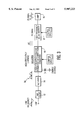
With reference now to FIG. 3, there can be seen a block diagram of an electronic ballast system 50 which constitutes a presently preferred embodiment of the present invention. As with the conventional ballast system described hereinabove, the ballast system 50 of the present invention includes an EMI filter 52 and a rectifier 56, e.g., a half-bridge or full-bridge rectifier. However, rather than the non-isolated boost converter of the conventional ballast system the ballast system 50 of the present invention includes a high-frequency PFC converter 58 which incorporates an isolation transformer (not shown in FIG. 3) which isolates the AC utility line and the lamp 60. An energy storage capacitor Ce is connected across the PFC converter 58 on the primary side of the isolation transformer. The output of the isolated PFC converter 58 is a DC voltage which is well-regulated by the control circuit A. This well-regulated DC voltage is then inverted into a high-frequency AC voltage by a high-frequency DC-AC inverter 62, e.g., a standard half-bridge or full-bridge AC-DC inverter or a half-bridge or full-bridge PWM AC-DC inverter. The high-frequency AC voltage produced by the DC-AC inverter 62 is delivered to the lamp 60 as a sinusoidal (AC) current for ignition thereof The control circuit B regulates the sinusoidal lamp current. The switching frequency of the PFC converter 58 is significantly higher than the switching frequency of the DC-AC inverter 62, which is the same as the lamp current frequency. In this connection, the switching frequency of the PFC converter 58 is preferably >500 kHz, whereas the switching frequency of the DC-AC inverter 62 and the lamp current frequency is preferably in the range of 25-50 kHz, in order to prevent excessive EMI radiation from the lamp 60, although the specific switching frequencies employed are not limiting to the present invention.
With reference now to FIG. 4, there can be seen a partial schematic, partial block diagram of an exemplary implementation of the above-described presently preferred embodiment of the present invention. With this particular implementation, the PFC converter 58 is comprised of a dither power factor correction circuit 70 and a high-frequency DC-DC converter 72. The dither power factor correction circuit 70 includes an inductor L1, diodes D1 and D2, MOSFET switches Q1 and Q2, and energy storage capacitor Ce. The DC-DC converter 72 includes the MOSFET switches Q1 and Q2, capacitors C1 and C2, transformer T, a full-bridge rectifier comprised of the diodes D3-D6, and capacitors C3 and C4. The DC-AC inverter 62 is a half-bridge inverter comprised of the capacitors C3 and C4, MOSFET switches Q3 and Q4, and an L-C tank circuit comprised of an inductor Lr and a capacitor Cr connected across the lamp 60.
With reference now to FIGS. 5A-5D, the operation of the dither power factor correction circuit 70 will now be described. With particular reference first to FIG. 5A, when the line voltage Vi is positive and the switch Q1 is turned on, the line voltage Vi is applied to the inductor L1 through the diode D1 and the switch Q1. The current through L1 rises linearly from zero to a positive peak value, and the energy is stored by the inductor L1.
With particular reference now to FIG. 5B, when the line voltage V1 is positive and the switch Q1 is turned off, the positive inductor current flows to the energy storage capacitor Ce through the body diode of the switch Q2, to thereby transfer the energy stored in the inductor L1 when the switch Q1 is turned on, to the energy storage capacitor Ce. The current through the inductor L1 falls linearly from its positive peak value to zero.
With particular reference now to FIG. 5C, when the line voltage V1 is negative and the switch Q2 is turned on, the line voltage V1 is applied to the inductor L1 through the diode D2 and the switch Q2. The current through L1 rises linearly from zero to a negative peak value, and the energy is stored by the inductor L1.
With particular reference to FIG. 5D, when the line voltage Vi is negative and the switch Q2 is turned off, the negative inductor current flows to the energy storage capacitor Ce through the body diode 78 of the switch Q1, to thereby transfer the energy stored in the inductor L1 when the switch Q2 is turned on, to the energy storage capacitor Ce. The current through the inductor L1 falls linearly from its negative peak value to zero.
With reference again to FIG. 4, the control circuit A receives a full-wave rectified feedback signal from the output of the DC-DC converter 72, and modulates the switching frequency of the switches Q1 and Q2 in such a manner as to effect power factor correction. The switches Q1 and Q2 are turned on and off in complementary fashion, with a nominal 50% duty ratio, at high frequency, e.g., >500 kHz, so that the current through the inductor L1 is in discontinuous conduction mode (DCM). After the high-frequency components of the current through the inductor L1 are filtered by the EMI filter 52, the line current is a semi-sinusoidal wave in phase with the line voltage. The power factor is close to unity and the total harmonic distortion is low. Thus, the input power is controlled by the frequency modulation of the MOSFET switches Q1 and Q2.
With reference now to FIG. 6, there can be seen the equivalent circuit for the DC-DC converter 72, in which the secondary side is reflected to the primary side, and the output is replaced by a voltage source Vo. As can be seen, the transformer T has leakage inductances Llk1 and Llk2, and a magnetizing inductance Lm. Before the switch Q1 is turned on, the current ilk2 is negative. After the switch Q1 is turned on, a positive voltage V1 is applied to the primary side of the transformer T, but a negative voltage Vo is applied to the secondary side of the transformer T through the diodes D4 and D6. The current ilk1 flowing through Llk1 and the current im flowing through Lm rise up. When ilk1 exceeds im, the current ilk2 (=ilk1-im) through Llk2 becomes positive and flows through diodes D3 and D5. When the switch Q2 is turned on, the operation is similar, but in reverse. The operating waveforms are depicted in FIG. 7.
The DC-DC converter 72 can be designed to be operated with zero-voltage-switching in order to reduce switching losses and switching noise. In this connection, the duty ratio control signals A1, A2 applied by the control circuit A to the gates of the MOSFET switches Q1 and Q2, respectively, are held inactive during a dead time, so that both switches Q1 and Q2 are turned off during this dead time. During the dead time, the current ilk1 through the leakage inductance Llk1 is used to charge and discharge the drain-source capacitances Cds1 and Cds2 of the switches Q1 and Q2, respectively. If the energy stored in the leakage inductance Llk1 is not enough to effect complete charge and discharge of the drain-source capacitances Cds1 and Cds2, the energy stored in the magnetizing inductance continues to charge and discharge these capacitances. The DC-DC converter 72 can be designed for zero-voltage-switching over a full load and input voltage range.
With reference again to FIG. 4, the high-frequency half-bridge DC-AC inverter 62 is conveniently the same as that in the conventional ballast circuit, except that the isolation transformer is eliminated, due to its inclusion in the PFC converter 58. The control circuit B receives a lamp current feedback signal and, in response thereto, modulates the switching frequency of the switches Q3 and Q4, in such a manner as to regulate the sinusoidal lamp current to a nearly constant rms value. In the preferred embodiment, the switches Q3 and Q4 are turned on and off in complementary fashion, with a nominal 50% duty ratio, at a high frequency, e.g., 25-50 kHz. Thus, the output power is regulated by the frequency modulation of the switches Q3 and Q4.
If the resonant frequency of the L-C circuit (Lr, Cr) is lower than the switching frequency of the DC-AC inverter 62, the inverter 62 can also be designed to be operated with zero-voltage-switching in order to reduce switching losses and switching noise. In this connection, the duty ratio control signals B1, B2 applied by the control circuit B to the gates of the MOSFET switches Q3 and Q4, respectively, are held inactive during a specified dead time, so that both switches Q3 and Q4 are turned off during this dead time.
With reference now to FIG. 8, there can be seen a first alternative embodiment of the ballast system of the present invention, which is the same as the exemplary implementation of the presently preferred embodiment depicted in FIG. 4, except that a high-frequency half-bridge PFC converter 80 is substituted for the high-frequency dither PFC converter 58. The half-bridge PFC converter 80 is comprised of a half-bridge power factor correction circuit 82 and a DC-DC converter 84. The half-bridge power factor correction circuit 82 includes a full-bridge rectifier comprised of diodes D1-D4, an inductor L1 and diode D5, MOSFET switches Q1 and Q2, and energy storage capacitor Ce. The DC-DC converter 84 is comprised of the MOSFET switches Q1 and Q2, capacitors C1 and C2, transformer T, a full-bridge rectifier comprised of diodes D6-D9, and capacitors C3 and C4.
With reference now to FIG. 9, there can be seen a second alternative embodiment of the ballast system of the present invention, which is the same as the exemplary implementation of the presently preferred embodiment depicted in FIG. 4, except that a high-frequency push-pull PFC converter 90 is substituted for the high-frequency dither PFC converter 58. The push-pull PFC converter 90 is comprised of a push-pull power factor correction circuit 92 and a DC-DC converter 94. The push-pull power factor correction circuit 92 includes an inductor L1 and diode D5 connected in series between a node N1 and a first terminal 96 of the primary winding of the transformer T, and an inductor L2 and diode D6 connected in series between the node N1 and a second terminal 98 of the primary winding of the transformer T, in parallel with the inductor L1 and diode D5. The node N1 is coupled to the output junction node N2 of a full-bridge rectifier comprised of diodes D1-D4. A first MOSFET switch Q1 is connected between the first terminal 96 of the primary winding of the transformer T and bottom rail 99, and a second MOSFET switch Q2 is connected between the second terminal 98 of the primary winding of the transformer T and the bottom rail 99, in parallel with the first switch Q1. The energy storage capacitor Ce is connected between the center tap 100 of the transformer T and the bottom rail 99. The remaining elements of the ballast system of this embodiment are the same as the corresponding elements of the ballast system of the presently preferred embodiment described hereianbove, and thus, a description thereof will be omitted.
With reference now to FIG. 10, there can be seen a third alternative embodiment of the ballast system of the present invention, which is the same as the exemplary implementation of the presently preferred embodiment of the present invention depicted in FIG. 4, except that a high-frequency pulse-width modulated (PWM) DC-AC inverter 110 is substituted for the standard half-bridge DC-AC inverter 62. The PWM DC-AC inverter 110 may be a half-bridge PWM inverter as shown in FIG. 11, or a full-bridge PWM inverter as shown in FIG. 12. The half-bridge PWM inverter works in the following manner. The pulse width of the duty ratio control signals B1, B2 issued by the control circuit B are modulated by a relatively low-frequency signal (e.g., a 25-50 kHz signal), resulting in a pulse-width modulated voltage Vab across points a and b. This pulse-width modulated voltage Vab is filtered by the L-C circuit comprised of the inductor Lo and the capacitor Co, to thereby produce a regulated, relatively low frequency output voltage (e.g., 25-50 kHz AC voltage) for driving the lamp 60. The corner frequency of the L-C filter can be designed for operation at a frequency at least one decade higher than the modulation frequency, e.g., 250 kHz, thereby enabling the size of the L-C filter to be significantly reduced. The switching frequency of the PWM inverter 110 (i.e., the nominal frequency of the duty ratio control signals B1, B2) can be at least one decade higher than the corner frequency of the L-C filter, e.g., 2.5 MHz. During ignition of the lamp 60, the modulation frequency is on the same order as the corner frequency of the L-C filter so that a high-voltage output can be obtained to ignite the lamp 60, due to resonance of the L-C circuit. During steady-state operation of the lamp 60, the modulation frequency is kept to 25 kHz in order to prevent excessive EMI radiation from the lamp 60. Thus, the control circuit B regulates the lamp current by current mode control. The operating waveforms for the half-bridge PWM DC-AC inverter are depicted in FIG. 13, and the operating waveforms for the full-bridge PWM DC-AC inverter are depicted in FIG. 14.
Although a presently preferred and various alternative embodiments of the present invention have been described in detail hereinabove, it should be clearly understood that many variations and/or modifications of the basic inventive concepts herein taught which may appear to those skilled in the pertinent art will fall within the spirit and scope of the present invention as defined in the appended claims. In this connection, for a more detailed understanding of various elements and facets of the present invention, and permissible variations thereof, reference is made to the following references.
Namely, for a more detailed understanding of power factor correction converters and DC-DC converters, reference is made to:
D. Chambers and D. Wang, "Dynamic power factor correction in capacitor input off line converters", POWERCON '79 Proceedings, pp. B3-1-B3-6, May, 1979;
C. Zhou and M. M. Jovanovic, "Design trade-offs in continous current-mode controlled boost power factor correction circuits", High Frequency Power Conversion Conference Record '92, pp. 202-220, May, 1992,
C. Solva, "Power factor correction with UC3854", Application Note, Unitrode Integrated Circuit,
C. Zhou, "Design and analysis of an active power factor correction circuit", M. S. Thesis, Virginia Polytechnique Institute and State University, Blacksburg, Va., May 1990;
C. P. Henze, "A digitally controlled AC to AC power conditioner that draws sinusoidal input current", IEEE PESC '86 Record, June 1986;
R. Erickson, M. Madigan and S. Singer, "Design of a simple high power factor rectifier based on the flyback converter", IEEE APEC '90 Proceedings, pp. 792-801, February 1990;
W. Tang, Y. Jiang, G. C. Hua and F. C. Lee, "Power factor correction with flyback converter employing charge control", VPEC Seminar '92 Proceeding, Virginia Polytechnique Institute and State University, Blacksburg, Va., September 1992;
M. H. Kheraluwala, R. L. Steigerwald and R. Gurumoorthy, "A fast response high power factor converter with a single power stage", IEEE PESC '91 Record, pp. 769-779, June 1991;
M. Madigan, R. Erickson and E. Ismail, "Integrated high quality rectifier-regulator", IEEE PESC '92, pp. 1043-1051, June 1992;
I. Takahashi and R. Y. Igarashi, "A swtiching power supply of 99% power factor by dither rectifier", IEEE INTELEC '91 Proceedings, pp. 714-719, November 1991;
Y. Jiang, G. C. Hua, W. Tang and F. C. Lee, "A novel single-phase power factor correction scheme", VPEC Seminar '92 Proceedings, Virginia Polytechnique Institute and State University, Blacksburg, Va., September 1992; and,
B. A. Miwa, D. M. Otten and M. F. Schlect, "High-efficiency power factor converter using interleaving techniques", IEEE APEC '92 Proceedings, pp. 557-568, February 1992.
For a more detailed understanding of zero-voltage-switching and soft-switching converters, including PWM DC-AC converters/inverters, reference is made to:
C. P. Henze, H. C. Martin and D. W. Parley, "Zero-voltage-switching in high-frequency power converters using pulse width modulation", Proceedings of 1988 IEEE Applied Power Electronics Conference, pp. 33-40, February 1988;
R. W. Erickson, A. F. Hernandez, A. F. Witulski and R. Xu, "A nonlinear resonant switch", Record of 1989 IEEE Power Electronics Specialists Conference, pp. 43-50, June 1989;
V. Vorperian, "Quasi-square-wave converters: topologies and analysis", IEEE, Transactions on Power Electronics, Vol. 3, No. 2, pp. 183-191, April 1988;
K. Watanabe, S. Takeishi, I. Norigoe and R. Hiramatsu, "Self running converter utilizing partial resonance", Proceeding of 1988 IEEE International Telecommunication Energy Conference, pp. 186-193, October 1988;
K. Harada and H. Sakamoto, "Non-resonant converter for mega hertz switching", Record of 1989 IEEE Power Electronics Specialists Conference, pp. 889-894, June 1989;
K. Harada and H. Sakamoto, "Switched-snubber for high-frequency switching", Record of 1990 IEEE Power Electronics Specialists Conference, pp. 181-188, June 1990;
K. Harada and H. Sakamoto, "On the saturable inductor commutation for zero-voltage-switching", Record of 1989 IEEE Power Electronics Specialists Conference, pp. 189-196, June 1990;
G. C. Hua, F. C. Lee and M. M. Jovanovic, "An improved zero-voltage-switched PWM converter using a saturable inductor", Record of 1989 IEEE Power Electronics Specialists Conference, pp. 189-194, June 1991;
W. J. Gu and K. Harada, "Novel self-excited PWM converters with zero-voltage-switched resonant transition using a saturable core", Proceedings of 1992 IEEE Applied Power Electronics Conference, pp. 58-65, February 1992;
W. J. Gu and K. Harada, "A novel, self-excited, PWM forward converter with ZVS resonant transition using two minor-loop-operated saturable cores", Record of 1992 IEEE Power Electronics Specialists Conference, pp. 85-92, June 1992;
G. C. Hua, C. S. Leu and F. C. Lee, "Novel zero-voltage-transition PWM converters", Record of 1992 IEEE Power Electronics Specialists Conference, pp. 55-61, June 1992;
U.S. Pat. No. 3,517,300, issued to W. McMurray, Jun. 23, 1970; and,
K. Harada, H. Sakamoto, and M. Shoyama, "Phase-controlled DC-AC converter", IEEE Transactions on Power Electronics, Vol. 3, No. 4, pp. 406-411, October 1988.
For a more detailed understanding of ballast systems, in general, reference is made to:
B. M. Wolfframm, "Ballasts-past, present, and future", Record of the 1984 IEEE Industry Application Society Annual Meeting, pp. 1288-1292, 1984;
R. J. Haver, "Electronic Ballasts", PCIM Magazine, pp. 52-56, April 1986;
R. Verderber, O. Morse and F. M. Rubinstein, "Performance of electronic ballast and controls with 34- and 40-Watt F40 fluorescent lamps", IEEE Transactions on Industry Applications, Vol. 25, No. 6, pp. 1049-1059, December 1989;
European Patent Application Publication Number 0507399A2, issued to Blom et al., and assigned to N. V. Philips;
U.S. Pat. No. 4,958,108, issued to Jorgensen, and assigned to Avtech Corporation;
U.S. Pat. No. 4,870,327, issued to Jorgensen, and assigned to Avtech Corporation; and,
U.S. Pat. No. 4,412,156, issued to Ota, and assigned to Elmo Company.
Claims (16)
1. A ballast system for a lamp, comprising:
rectifier means for rectifying AC input power having a first frequency and producing a pulsating DC current;
a DC-DC converter for converting said pulsating DC current into a substantially constant DC voltage, said DC-DC converter including an isolation transformer having a primary side and a secondary side and a power factor correction circuit provided on said primary side of said isolation transformer, said power factor correction circuit including an inductor and an energy storage capacitor;
second converter means provided on said secondary side of said isolation transformer for converting said constant DC voltage into an AC output current having a second frequency, said second frequency being higher than said first frequency; and
power application means responsive to said AC output current for powering the lamp;
wherein said power factor correction circuit and said DC-DC converter include, in common, a first switching means for regulating conduction of current through said inductor and transfer of energy stored in said inductor to said energy storage capacitor, and first control means for operating said first switching means at a first switching frequency, and for modulating the switching frequency of said first switching means to effect power factor correction.
2. The ballast system as set forth in claim 1, wherein said power application means includes an L-C circuit having a resonant frequency, said L-C circuit producing a sinusoidal lamp current for powering the lamp.
3. The ballast system as set forth in claim 2, wherein said resonant frequency is substantially equal to said second frequency.
4. The ballast system as set forth in claim 2, wherein said second converter means includes second switching means and second control means for operating said second switching means at a second switching frequency.
5. The ballast system as set forth in claim 4, wherein said first switching frequency is higher than said second switching frequency.
6. The ballast system as set forth in claim 5, wherein said second switching frequency is substantially the same as said second frequency.
7. The ballast system as set forth in claim 5, wherein said first switching frequency is at least ten times higher than said second switching frequency.
8. The ballast system as set forth in claim 5, wherein said power factor correction circuit comprises a dither power factor correction circuit.
9. The ballast system as set forth in claim 4, wherein said second converter means comprises a half-bridge DC-AC inverter.
10. The ballast system as set forth in claim 4, wherein said second converter means comprises a full-bridge DC-AC inverter.
11. The ballast system as set forth in claim 4, wherein:
said second converter means comprises a PWM DC-AC inverter;
said second switching frequency is higher than said first switching frequency; and,
said second control means modulates the duty ratio of said second switching means at a modulation frequency which is lower than said first switching frequency.
12. The ballast system as set forth in claim 4, wherein said second control means is responsive to a lamp current feedback signal for modulating the switching frequency of said second switching means, to thereby regulate said lamp current.
13. The ballast system as set forth in claim 12, wherein said first and second switching means are adapted for zero-voltage-switching.
14. The ballast system as set forth in claim 1, wherein said second converter means includes second switching means and second control means for operating said second switching means at a second switching frequency, said first switching frequency being higher than said second switching frequency.
15. The ballast system as set forth in claim 14, wherein said second switching frequency is substantially the same as said second frequency.
16. The ballast system as set forth in claim 15, wherein said first switching frequency is at least ten times higher than said second switching frequency.
Priority Applications (1)
| Application Number | Priority Date | Filing Date | Title |
|---|---|---|---|
| US08/891,879 US5907223A (en) | 1995-12-08 | 1997-07-09 | Two-frequency electronic ballast system having an isolated PFC converter |
Applications Claiming Priority (2)
| Application Number | Priority Date | Filing Date | Title |
|---|---|---|---|
| US56951595A | 1995-12-08 | 1995-12-08 | |
| US08/891,879 US5907223A (en) | 1995-12-08 | 1997-07-09 | Two-frequency electronic ballast system having an isolated PFC converter |
Related Parent Applications (1)
| Application Number | Title | Priority Date | Filing Date |
|---|---|---|---|
| US56951595A Continuation | 1995-12-08 | 1995-12-08 |
Publications (1)
| Publication Number | Publication Date |
|---|---|
| US5907223A true US5907223A (en) | 1999-05-25 |
Family
ID=24275761
Family Applications (1)
| Application Number | Title | Priority Date | Filing Date |
|---|---|---|---|
| US08/891,879 Expired - Fee Related US5907223A (en) | 1995-12-08 | 1997-07-09 | Two-frequency electronic ballast system having an isolated PFC converter |
Country Status (7)
| Country | Link |
|---|---|
| US (1) | US5907223A (en) |
| EP (1) | EP0808552B1 (en) |
| JP (1) | JPH11500861A (en) |
| CN (1) | CN1156200C (en) |
| DE (1) | DE69626796T2 (en) |
| TW (1) | TW347642B (en) |
| WO (1) | WO1997022232A1 (en) |
Cited By (68)
| Publication number | Priority date | Publication date | Assignee | Title |
|---|---|---|---|---|
| US6107754A (en) * | 1999-01-02 | 2000-08-22 | Inlight Co., Ltd. | Electronic ballast for high-intensity discharge lamp and method of driving high-intensity discharge lamp |
| US6174067B1 (en) | 1998-04-21 | 2001-01-16 | Pacfab, Inc. | Lighting system, apparatus, and method |
| US6181079B1 (en) * | 1999-12-20 | 2001-01-30 | Philips Electronics North America Corporation | High power electronic ballast with an integrated magnetic component |
| US6313585B1 (en) * | 1997-04-24 | 2001-11-06 | Mannesmann Vdo Ag | Method for dimming a fluorescent lamp arranged in the secondary circuit of a transformer and arrangement to implement said method |
| US6377000B2 (en) * | 1999-12-03 | 2002-04-23 | Joong Seong Kim | Electronic ballast for gas discharge lamp |
| US6407935B1 (en) * | 2000-05-30 | 2002-06-18 | Koninklijke Philips Electronics N.V. | High frequency electronic ballast with reactive power compensation |
| US6429604B2 (en) * | 2000-01-21 | 2002-08-06 | Koninklijke Philips Electronics N.V. | Power feedback power factor correction scheme for multiple lamp operation |
| US6483721B2 (en) * | 2000-01-28 | 2002-11-19 | Densei-Lambda K.K. | Resonant power converter |
| WO2002093726A1 (en) * | 2001-05-17 | 2002-11-21 | Abb Ab | An apparatus and a method for voltage conversion |
| US6556463B1 (en) * | 1999-09-27 | 2003-04-29 | Valeo Vision | Reduced electronic noise power supply to discharge lamps, especially for motor vehicle headlights |
| US6556457B1 (en) * | 2002-01-03 | 2003-04-29 | Kokusan Denki Co., Ltd. | Method of controlling inverter power generation apparatus |
| US6580259B2 (en) * | 2001-01-17 | 2003-06-17 | The University Of Hong Kong | High efficiency AC-DC converter with power factor corrector |
| US6600271B1 (en) * | 1998-06-09 | 2003-07-29 | Laplaz Light Co. Inc. | Method and apparatus of an improved electronics ballast circuit |
| US6600273B2 (en) * | 2000-12-23 | 2003-07-29 | Samsung Electro-Mechanics Co., Ltd. | High-power electronic ballast for fluorescent lamp |
| US20030146714A1 (en) * | 2001-12-19 | 2003-08-07 | Nicholas Buonocunto | Electronic ballast system having emergency lighting provisions |
| US20040075965A1 (en) * | 2001-12-31 | 2004-04-22 | Lewis James M. | MOSFET based, high voltage, electronic relays for AC power switching and inductive loads |
| US20040130917A1 (en) * | 2001-04-10 | 2004-07-08 | Siemens Aktiengesellschaft | Method and voltage converter for converting DC input voltage to AC voltage in a system frequency range |
| US20040155607A1 (en) * | 1998-12-11 | 2004-08-12 | Rust Timothy James | Method for starting a discharge lamp using high energy initial pulse |
| WO2004095668A2 (en) * | 2003-04-23 | 2004-11-04 | Matsushita Electric Works, Ltd. | Discharge lamp lighting control device |
| US20050012467A1 (en) * | 2003-07-18 | 2005-01-20 | Nemirow Arthur T. | Fluorescent lamp electronic ballast |
| US20050068706A1 (en) * | 2001-12-31 | 2005-03-31 | Lewis James M. | Driver system for MOSFET based, high voltage, electronic relays for AC power switching and inductive loads |
| US20050082914A1 (en) * | 2001-12-31 | 2005-04-21 | Lewis James M. | Mosfet based, high voltage, electronic relays for AC power switching and inductive loads |
| US20050248289A1 (en) * | 2002-07-30 | 2005-11-10 | Koninklijke Philips Electronics N.V. | Driver for a gas discharge lamp |
| US20050258778A1 (en) * | 2004-05-19 | 2005-11-24 | Wei Chen | Method and apparatus for single-ended conversion of DC to Ac power for driving discharge lamps |
| US20060113922A1 (en) * | 2004-10-29 | 2006-06-01 | International Rectifier Corporation | HID buck and full-bridge ballast control IC |
| EP1687891A1 (en) * | 2003-11-25 | 2006-08-09 | Electric Power Research Institute, Inc | Multilevel converter based intelligent universal transformer |
| US20060226817A1 (en) * | 2005-04-07 | 2006-10-12 | Patent-Treuhand-Gesellschaft Fur Elektrisch Gluhlampen Mbh | Metal halide lamp |
| US20060238138A1 (en) * | 2005-04-21 | 2006-10-26 | Energy Conservation Technologies, Inc. | Control circuit for maintaining constant power in power factor corrected electronic ballasts and power supplies |
| US20060284568A1 (en) * | 2005-06-17 | 2006-12-21 | Hon Hai Precision Industry Co., Ltd. | Power supply system for flat panel display devices |
| US20070024208A1 (en) * | 2003-09-17 | 2007-02-01 | Koninklijke Philips Electronics N.V. | Circuit arrangement and method of operating a gas discharge lamp |
| US20070101378A1 (en) * | 2003-05-02 | 2007-05-03 | Koninklijke Philips Electronics N.V. | Redundant transmission of programmes |
| US20070133144A1 (en) * | 2001-12-31 | 2007-06-14 | Lewis James M | Driver system for MOSFET based, high voltage electronic relays for AC power switching and inductive loads |
| US20070228994A1 (en) * | 2006-04-04 | 2007-10-04 | Delta Optoelectronics, Inc. | Driving circuit and method for fluorescent lamp |
| US20080024072A1 (en) * | 2006-07-27 | 2008-01-31 | Chien-Chih Chen | Acoustic resonance free driving electronic ballast for high intensity discharge lamp |
| ES2296459A1 (en) * | 2005-07-06 | 2008-04-16 | Universidad De Oviedo | High power factor integrated electronic ballast for feeding lamps of high pressure discharging, has converter gearbox setback for power factor correction, and another to control power of lamp, and output converter setback coil is provided |
| US20080088255A1 (en) * | 2006-10-11 | 2008-04-17 | Hon Hai Precision Industry Co., Ltd. | Device for driving light source module |
| WO2008116561A1 (en) | 2007-03-28 | 2008-10-02 | Tridonicatco Gmbh & Co.Kg | Error detector in an operating device for lighting devices |
| US7525293B1 (en) * | 2004-12-06 | 2009-04-28 | Marvell International Ltd. | Power supply switching circuit for a halogen lamp |
| US20090251060A1 (en) * | 2008-03-31 | 2009-10-08 | Nicollet Technologies Corporation | Electronic ballast system with lamp interface network |
| US20090251114A1 (en) * | 2004-05-12 | 2009-10-08 | Merstech, Inc. | Alternating-current power supply device recovering magnetic energy |
| EP2110937A1 (en) * | 2007-01-30 | 2009-10-21 | Panasonic Electric Works Co., Ltd | Insulation type ac-dc converter and led dc power supply device using the same |
| WO2010051984A3 (en) * | 2008-11-05 | 2010-07-15 | Tridonicatco Gmbh & Co.Kg | Illuminant operating appliance with potential separation |
| US20100254163A1 (en) * | 2007-12-07 | 2010-10-07 | Osram Gesellschaft Mit Beschraenkter Haftung | Resonant power converter with current doubler rectifier and related method |
| US20100320926A1 (en) * | 2009-06-17 | 2010-12-23 | Kun-Pai Hsu | Sine wave light modulation control method and device |
| EP2276157A1 (en) * | 2009-07-17 | 2011-01-19 | Huawei Technologies Co., Ltd. | Power converter, device and method for interleaving controlling power factor correction circuits |
| US20110032734A1 (en) * | 2008-04-29 | 2011-02-10 | Melanson John L | Cascaded switching power converter for coupling a photovoltaic energy source to power mains |
| US20110031916A1 (en) * | 2005-08-31 | 2011-02-10 | David Bonner | Inverter Circuit with IPM Module for Brushless Motor |
| US7924584B1 (en) | 2004-01-29 | 2011-04-12 | Marvell International Ltd. | Power supply switching circuit for a halogen lamp |
| US20110273118A1 (en) * | 2010-05-10 | 2011-11-10 | David Bonner | Power Factor Correction Circuit |
| CN102299649A (en) * | 2010-06-24 | 2011-12-28 | 盛飞 | Power supply converter |
| NL2005041C2 (en) * | 2010-07-06 | 2012-01-10 | Online Services B V | High-frequency switching-mode ballast device for a dimming circuit. |
| US20120032708A1 (en) * | 2010-08-03 | 2012-02-09 | Microsemi Corporation | Gate driver power and control signal transmission circuits and methods |
| US20120037616A1 (en) * | 2008-10-27 | 2012-02-16 | Merstech Inc. | Power inverter |
| US20130020966A1 (en) * | 2011-07-19 | 2013-01-24 | Delta Electronics (Shanghai) Co., Ltd. | Method and circuit for improving crest factor of gas discharge lamp |
| KR101234829B1 (en) * | 2008-01-14 | 2013-02-20 | 삼성전자주식회사 | Device for power factor correction in three phase power supply |
| WO2013116374A1 (en) * | 2012-02-01 | 2013-08-08 | Dialight Corporation | Independently adjustable current and voltage ac-ac converter |
| US8742690B2 (en) | 2009-01-09 | 2014-06-03 | Tridonic Gmbh And Co Kg | Method, operating device, and lighting system |
| US20150032096A1 (en) * | 2013-07-24 | 2015-01-29 | Covidien Lp | Systems and methods for generating electrosurgical energy using a multistage power converter |
| US20150042242A1 (en) * | 2013-08-09 | 2015-02-12 | Osram Sylvania Inc. | Output current configuration based on load connection |
| US20150224885A1 (en) * | 2012-11-01 | 2015-08-13 | Myongji University Industry And Academia Cooperation Foundation | Device for compensating for ripples of output voltage of pfc converter and battery charging device for electric vehicle using same |
| US20150288275A1 (en) * | 2014-04-08 | 2015-10-08 | Ionel Jitaru | Input Current Distortion for Minimization of Bulk Capacitor |
| US20150334797A1 (en) * | 2012-12-28 | 2015-11-19 | Tridonic Gmbh & Co Kg | Operation of an illuminant by means of a resonant converter |
| US20160190954A1 (en) * | 2014-12-31 | 2016-06-30 | Avogy, Inc. | Method and system for bridgeless ac-dc converter |
| EP3038246A3 (en) * | 2013-03-14 | 2016-10-12 | Vanner, Inc. | Dc-ac conversion circuit topologie |
| US20160380549A1 (en) * | 2013-11-29 | 2016-12-29 | Hep Tech Co., Ltd. | Ac-ac power source conversion device and conversion method thereof |
| US10003267B1 (en) | 2016-12-19 | 2018-06-19 | Analog Devices Global | Isolated DC-DC converter with an H-bridge circuit |
| US11418125B2 (en) | 2019-10-25 | 2022-08-16 | The Research Foundation For The State University Of New York | Three phase bidirectional AC-DC converter with bipolar voltage fed resonant stages |
| US20220263402A1 (en) * | 2020-03-25 | 2022-08-18 | Delta Electronics (Shanghai) Co., Ltd. | Control method for power supply |
Families Citing this family (10)
| Publication number | Priority date | Publication date | Assignee | Title |
|---|---|---|---|---|
| US6084786A (en) * | 1999-01-29 | 2000-07-04 | Hamilton Sundstrand Corporation | Converter system with power factor and DC ripple control |
| FR2794302B1 (en) * | 1999-05-28 | 2001-07-13 | Ptc | METHOD AND DEVICE FOR SUPPLYING, WITH GALVANIC INSULATION, AN ELECTRICAL APPARATUS AT A VERY LOW SECURITY VOLTAGE |
| FR2804570B1 (en) | 2000-01-27 | 2002-07-19 | Eclairage Public Beep Bureau E | MODULAR ELECTRONIC SUPPLY DEVICE FOR DISCHARGE LAMP |
| ES2180386B1 (en) * | 2000-07-31 | 2004-04-01 | Universidad De Oviedo. | TWO ELECTRONIC CIRCUITS FOR POWERING DISCHARGE LAMPS WITH ACTIVE CORRECTION OF THE POWER FACTOR BASED ON TOPOLOGIES OF A SINGLE STAGE. |
| US6686703B2 (en) * | 2002-01-10 | 2004-02-03 | Koninklijke Philips Electronics N.V. | High frequency electronic ballast |
| US6667585B2 (en) * | 2002-02-20 | 2003-12-23 | Northrop Grumman Corporation | Fluorescent lamp brightness control process by ballast frequency adjustment |
| DE10333820A1 (en) | 2003-07-24 | 2005-02-17 | Patent-Treuhand-Gesellschaft für elektrische Glühlampen mbH | Circuit arrangement for operating at least one high-pressure discharge lamp |
| US7885085B2 (en) * | 2007-01-22 | 2011-02-08 | Power Integrations, Inc. | Cascaded PFC and resonant mode power converters |
| CN106338645B (en) * | 2016-11-09 | 2019-06-04 | 广州视源电子科技股份有限公司 | A kind of current sampling device and its method of frequency converter |
| CN109818427A (en) * | 2019-03-26 | 2019-05-28 | 华南理工大学 | The output modulation circuit and its metal-oxide-semiconductor control method of wireless power transmission systems receiving side |
Citations (8)
| Publication number | Priority date | Publication date | Assignee | Title |
|---|---|---|---|---|
| US3517300A (en) * | 1968-04-16 | 1970-06-23 | Gen Electric | Power converter circuits having a high frequency link |
| US4412156A (en) * | 1980-09-03 | 1983-10-25 | Elmo Company, Limited | Power supply for an ac discharge lamp |
| US4441053A (en) * | 1981-11-27 | 1984-04-03 | Data-Design Laboratories | Switched mode electrode ballast |
| US4870327A (en) * | 1987-07-27 | 1989-09-26 | Avtech Corporation | High frequency, electronic fluorescent lamp ballast |
| US4958108A (en) * | 1989-02-14 | 1990-09-18 | Avtech Corporation | Universal fluorescent lamp ballast |
| EP0507399A2 (en) * | 1991-04-04 | 1992-10-07 | Koninklijke Philips Electronics N.V. | Circuit arrangement |
| US5371440A (en) * | 1993-12-28 | 1994-12-06 | Philips Electronics North America Corp. | High frequency miniature electronic ballast with low RFI |
| US5416387A (en) * | 1993-11-24 | 1995-05-16 | California Institute Of Technology | Single stage, high power factor, gas discharge lamp ballast |
Family Cites Families (2)
| Publication number | Priority date | Publication date | Assignee | Title |
|---|---|---|---|---|
| EP0439861A1 (en) * | 1990-01-29 | 1991-08-07 | Koninklijke Philips Electronics N.V. | Circuit arrangement |
| JPH04138066A (en) * | 1990-09-26 | 1992-05-12 | Toshiba Lighting & Technol Corp | Device for lighting discharge lamp |
-
1996
- 1996-11-22 WO PCT/IB1996/001289 patent/WO1997022232A1/en active IP Right Grant
- 1996-11-22 DE DE69626796T patent/DE69626796T2/en not_active Expired - Fee Related
- 1996-11-22 EP EP96937456A patent/EP0808552B1/en not_active Expired - Lifetime
- 1996-11-22 CN CNB961918403A patent/CN1156200C/en not_active Expired - Fee Related
- 1996-11-22 JP JP9521875A patent/JPH11500861A/en not_active Withdrawn
-
1997
- 1997-01-14 TW TW086100346A patent/TW347642B/en active
- 1997-07-09 US US08/891,879 patent/US5907223A/en not_active Expired - Fee Related
Patent Citations (8)
| Publication number | Priority date | Publication date | Assignee | Title |
|---|---|---|---|---|
| US3517300A (en) * | 1968-04-16 | 1970-06-23 | Gen Electric | Power converter circuits having a high frequency link |
| US4412156A (en) * | 1980-09-03 | 1983-10-25 | Elmo Company, Limited | Power supply for an ac discharge lamp |
| US4441053A (en) * | 1981-11-27 | 1984-04-03 | Data-Design Laboratories | Switched mode electrode ballast |
| US4870327A (en) * | 1987-07-27 | 1989-09-26 | Avtech Corporation | High frequency, electronic fluorescent lamp ballast |
| US4958108A (en) * | 1989-02-14 | 1990-09-18 | Avtech Corporation | Universal fluorescent lamp ballast |
| EP0507399A2 (en) * | 1991-04-04 | 1992-10-07 | Koninklijke Philips Electronics N.V. | Circuit arrangement |
| US5416387A (en) * | 1993-11-24 | 1995-05-16 | California Institute Of Technology | Single stage, high power factor, gas discharge lamp ballast |
| US5371440A (en) * | 1993-12-28 | 1994-12-06 | Philips Electronics North America Corp. | High frequency miniature electronic ballast with low RFI |
Non-Patent Citations (28)
| Title |
|---|
| B.M. Wolfframm, "Ballasts-Past, Present, and Future", Record of the 1984 IEEE Industry Application Society Annual Meeting, pp. 1288-1292, 1984. |
| B.M. Wolfframm, Ballasts Past, Present, and Future , Record of the 1984 IEEE Industry Application Society Annual Meeting, pp. 1288 1292, 1984. * |
| C. Zhou et al, "Design Trade-Offs in Continous Current-Mode Controlled Boost Power Factor Correction Circuits", High Frequency Power Conversion Conference Record 92, pp. 202-220, May, 1992. |
| C. Zhou et al, Design Trade Offs in Continous Current Mode Controlled Boost Power Factor Correction Circuits , High Frequency Power Conversion Conference Record 92, pp. 202 220, May, 1992. * |
| C. Zhou, "Design and Analysis of an Active Power Factor Correction Circuit", M.S. Thesis, Virginia Polytechnique Institute and State University, Blacksburg, Virgina, May 1990. |
| C. Zhou, Design and Analysis of an Active Power Factor Correction Circuit , M.S. Thesis, Virginia Polytechnique Institute and State University, Blacksburg, Virgina, May 1990. * |
| C.P. Henze, "A Digitally Controlled AC to AC Power Conditioner That Draws Sinusoidal Input Current", IEEE PESC '86 Record, Jun. 1986. |
| C.P. Henze, A Digitally Controlled AC to AC Power Conditioner That Draws Sinusoidal Input Current , IEEE PESC 86 Record, Jun. 1986. * |
| D. Chambers et al, "Dynamic Power Factor Correction in Capacitor Input Offline Converters", Powercon '79 Proceedings, pp. B3-1-B3-6, May, 1979. |
| D. Chambers et al, Dynamic Power Factor Correction in Capacitor Input Offline Converters , Powercon 79 Proceedings, pp. B3 1 B3 6, May, 1979. * |
| G.C. Hua, C.S. Leu and F.C. Lee, "Novel Zero-Voltage-Transition PWM Converters", Record of 1992 IEEE Power Electronics Specialists Conference, pp. 55-61, Jun. 1992. |
| G.C. Hua, C.S. Leu and F.C. Lee, Novel Zero Voltage Transition PWM Converters , Record of 1992 IEEE Power Electronics Specialists Conference, pp. 55 61, Jun. 1992. * |
| K. Harada, H. Sakamoto, and M. Shoyama, "Phase-Controlled DC-AC Converter", IEEE Transactions on Power Electronics, vol. 3, No. 4, pp. 406-411, Oct. 1988. |
| K. Harada, H. Sakamoto, and M. Shoyama, Phase Controlled DC AC Converter , IEEE Transactions on Power Electronics, vol. 3, No. 4, pp. 406 411, Oct. 1988. * |
| M. Madigan, R. Erickson and E. Ismail, "Integrated High Quality Rectifier-Regulator", IEEE PESC '92, pp. 1043-1051, Jun. 1992. |
| M. Madigan, R. Erickson and E. Ismail, Integrated High Quality Rectifier Regulator , IEEE PESC 92, pp. 1043 1051, Jun. 1992. * |
| M.H. Kheraluwala, R.L. Steigerwald and R. Gurumoorthy, "A Fast Response High Power Factor Converter with a Single Power Stage", IEEE PESC '91 Record, pp. 769-779, Jun. 1991. |
| M.H. Kheraluwala, R.L. Steigerwald and R. Gurumoorthy, A Fast Response High Power Factor Converter with a Single Power Stage , IEEE PESC 91 Record, pp. 769 779, Jun. 1991. * |
| R. Erickson, M. Madigan and S. Singer, "Design of a Simple High Power Factor Rectifier Based on the Flyback Converter", IEEE APEC '90 Proceedings, pp. 792-801, Feb. 1990. |
| R. Erickson, M. Madigan and S. Singer, Design of a Simple High Power Factor Rectifier Based on the Flyback Converter , IEEE APEC 90 Proceedings, pp. 792 801, Feb. 1990. * |
| R. Verderber, O. Morse and F.M. Rubinstein, "Performance of Electronic Ballast and Controls With 34- and 40-Watt F40 Fluorescent Lamps", IEEE Transactions on Industry Applications, vol. 25, No. 6, pp. 1049-1059, Dec. 1989. |
| R. Verderber, O. Morse and F.M. Rubinstein, Performance of Electronic Ballast and Controls With 34 and 40 Watt F40 Fluorescent Lamps , IEEE Transactions on Industry Applications, vol. 25, No. 6, pp. 1049 1059, Dec. 1989. * |
| R.J. Haver, "Electronic Ballasts", PCIM Magazine, pp. 52-56, Apr. 1986. |
| R.J. Haver, Electronic Ballasts , PCIM Magazine, pp. 52 56, Apr. 1986. * |
| W. Tang, Y. Jiang, G.C. Hua and F.C. Lee, "Power Factor Correction with Flyback Converter Employing Charge Control", VPEC Seminar '92 Proceedings, Virginia Polytechnique Institute and State University, Blacksburg, Virginia, Sep. 1992. |
| W. Tang, Y. Jiang, G.C. Hua and F.C. Lee, Power Factor Correction with Flyback Converter Employing Charge Control , VPEC Seminar 92 Proceedings, Virginia Polytechnique Institute and State University, Blacksburg, Virginia, Sep. 1992. * |
| W.J. Gu and K. Harada, "A Novel, Self-Excited, PWM Forward Converter with ZVS Resonant Transition Using Two Minor-Loop-Operated Saturable Cores", Record of 1992 IEEE Power Electronics Specialists Conference, pp. 85-92, Jun. 1992. |
| W.J. Gu and K. Harada, A Novel, Self Excited, PWM Forward Converter with ZVS Resonant Transition Using Two Minor Loop Operated Saturable Cores , Record of 1992 IEEE Power Electronics Specialists Conference, pp. 85 92, Jun. 1992. * |
Cited By (128)
| Publication number | Priority date | Publication date | Assignee | Title |
|---|---|---|---|---|
| US6313585B1 (en) * | 1997-04-24 | 2001-11-06 | Mannesmann Vdo Ag | Method for dimming a fluorescent lamp arranged in the secondary circuit of a transformer and arrangement to implement said method |
| US6174067B1 (en) | 1998-04-21 | 2001-01-16 | Pacfab, Inc. | Lighting system, apparatus, and method |
| US6600271B1 (en) * | 1998-06-09 | 2003-07-29 | Laplaz Light Co. Inc. | Method and apparatus of an improved electronics ballast circuit |
| US20040155607A1 (en) * | 1998-12-11 | 2004-08-12 | Rust Timothy James | Method for starting a discharge lamp using high energy initial pulse |
| US7355354B2 (en) * | 1998-12-11 | 2008-04-08 | Monolithic Power Systems, Inc. | Method for starting a discharge lamp using high energy initial pulse |
| US6107754A (en) * | 1999-01-02 | 2000-08-22 | Inlight Co., Ltd. | Electronic ballast for high-intensity discharge lamp and method of driving high-intensity discharge lamp |
| US6556463B1 (en) * | 1999-09-27 | 2003-04-29 | Valeo Vision | Reduced electronic noise power supply to discharge lamps, especially for motor vehicle headlights |
| US6377000B2 (en) * | 1999-12-03 | 2002-04-23 | Joong Seong Kim | Electronic ballast for gas discharge lamp |
| US6181079B1 (en) * | 1999-12-20 | 2001-01-30 | Philips Electronics North America Corporation | High power electronic ballast with an integrated magnetic component |
| US6429604B2 (en) * | 2000-01-21 | 2002-08-06 | Koninklijke Philips Electronics N.V. | Power feedback power factor correction scheme for multiple lamp operation |
| US6483721B2 (en) * | 2000-01-28 | 2002-11-19 | Densei-Lambda K.K. | Resonant power converter |
| US6407935B1 (en) * | 2000-05-30 | 2002-06-18 | Koninklijke Philips Electronics N.V. | High frequency electronic ballast with reactive power compensation |
| US6600273B2 (en) * | 2000-12-23 | 2003-07-29 | Samsung Electro-Mechanics Co., Ltd. | High-power electronic ballast for fluorescent lamp |
| US6580259B2 (en) * | 2001-01-17 | 2003-06-17 | The University Of Hong Kong | High efficiency AC-DC converter with power factor corrector |
| EP1352463A1 (en) * | 2001-01-17 | 2003-10-15 | The University of Hong Kong | A high efficiency ac-dc converter with power factor corrector |
| US20030210024A1 (en) * | 2001-01-17 | 2003-11-13 | Liu Joe Chui Pong | High efficiency AC-DC converter with power factor corrector |
| EP1352463A4 (en) * | 2001-01-17 | 2009-01-21 | Univ Hong Kong | A high efficiency ac-dc converter with power factor corrector |
| US6812679B2 (en) | 2001-01-17 | 2004-11-02 | The University Of Hong Kong | High efficiency AC-DC converter with power factor corrector |
| US6944037B2 (en) * | 2001-04-10 | 2005-09-13 | Siemens Aktiengesellschaft | Method and voltage converter for converting DC input voltage to AC voltage in a system frequency range |
| US20040130917A1 (en) * | 2001-04-10 | 2004-07-08 | Siemens Aktiengesellschaft | Method and voltage converter for converting DC input voltage to AC voltage in a system frequency range |
| US6507503B2 (en) | 2001-05-17 | 2003-01-14 | Abb Ab | Apparatus and a method for voltage conversion |
| WO2002093726A1 (en) * | 2001-05-17 | 2002-11-21 | Abb Ab | An apparatus and a method for voltage conversion |
| US20030146714A1 (en) * | 2001-12-19 | 2003-08-07 | Nicholas Buonocunto | Electronic ballast system having emergency lighting provisions |
| US6784624B2 (en) * | 2001-12-19 | 2004-08-31 | Nicholas Buonocunto | Electronic ballast system having emergency lighting provisions |
| US7084582B2 (en) * | 2001-12-19 | 2006-08-01 | Nicolas Buonocunto | Electronic ballast system having emergency lighting provisions and electronic chip |
| US20050029966A1 (en) * | 2001-12-19 | 2005-02-10 | Nicholas Buonocunto | Electronic ballast system having emergency lighting provisions and electronic chip |
| US20050068706A1 (en) * | 2001-12-31 | 2005-03-31 | Lewis James M. | Driver system for MOSFET based, high voltage, electronic relays for AC power switching and inductive loads |
| US7102253B2 (en) * | 2001-12-31 | 2006-09-05 | Lewis James M | MOSFET based, high voltage, electronic relays for AC power switching and inductive loads |
| US20050082914A1 (en) * | 2001-12-31 | 2005-04-21 | Lewis James M. | Mosfet based, high voltage, electronic relays for AC power switching and inductive loads |
| US20040075965A1 (en) * | 2001-12-31 | 2004-04-22 | Lewis James M. | MOSFET based, high voltage, electronic relays for AC power switching and inductive loads |
| US7183672B2 (en) | 2001-12-31 | 2007-02-27 | Lewis James M | MOSFET based, high voltage, electronic relays for AC power switching and inductive loads |
| US7439636B2 (en) | 2001-12-31 | 2008-10-21 | Lewis James M | Driver system for MOSFET based, high voltage electronic relays for AC power switching and inductive loads |
| US7230354B2 (en) | 2001-12-31 | 2007-06-12 | Lewis James M | Driver system for MOSFET based, high voltage, electronic relays for AC power switching and inductive loads |
| US20070133144A1 (en) * | 2001-12-31 | 2007-06-14 | Lewis James M | Driver system for MOSFET based, high voltage electronic relays for AC power switching and inductive loads |
| US6556457B1 (en) * | 2002-01-03 | 2003-04-29 | Kokusan Denki Co., Ltd. | Method of controlling inverter power generation apparatus |
| US20050248289A1 (en) * | 2002-07-30 | 2005-11-10 | Koninklijke Philips Electronics N.V. | Driver for a gas discharge lamp |
| US7391165B2 (en) | 2003-04-23 | 2008-06-24 | Matsushita Electric Works, Ltd. | Discharge lamp lighting control device |
| US20060279230A1 (en) * | 2003-04-23 | 2006-12-14 | Matsushita Electric Works, Ltd. | Discharge lamp lighting control device |
| WO2004095668A3 (en) * | 2003-04-23 | 2005-03-24 | Matsushita Electric Works Ltd | Discharge lamp lighting control device |
| WO2004095668A2 (en) * | 2003-04-23 | 2004-11-04 | Matsushita Electric Works, Ltd. | Discharge lamp lighting control device |
| US20070101378A1 (en) * | 2003-05-02 | 2007-05-03 | Koninklijke Philips Electronics N.V. | Redundant transmission of programmes |
| US20050012467A1 (en) * | 2003-07-18 | 2005-01-20 | Nemirow Arthur T. | Fluorescent lamp electronic ballast |
| US7095185B2 (en) * | 2003-07-18 | 2006-08-22 | Bruce Industries, Inc. | Fluorescent lamp electronic ballast |
| US20070024208A1 (en) * | 2003-09-17 | 2007-02-01 | Koninklijke Philips Electronics N.V. | Circuit arrangement and method of operating a gas discharge lamp |
| EP1687891A1 (en) * | 2003-11-25 | 2006-08-09 | Electric Power Research Institute, Inc | Multilevel converter based intelligent universal transformer |
| EP1687891A4 (en) * | 2003-11-25 | 2012-11-14 | Electric Power Res Inst | Multilevel converter based intelligent universal transformer |
| US7924584B1 (en) | 2004-01-29 | 2011-04-12 | Marvell International Ltd. | Power supply switching circuit for a halogen lamp |
| US20090251114A1 (en) * | 2004-05-12 | 2009-10-08 | Merstech, Inc. | Alternating-current power supply device recovering magnetic energy |
| US7843166B2 (en) * | 2004-05-12 | 2010-11-30 | Merstech, Inc. | Alternating-current power supply device recovering magnetic energy |
| US7161305B2 (en) * | 2004-05-19 | 2007-01-09 | Monolithic Power Systems, Inc. | Method and apparatus for single-ended conversion of DC to AC power for driving discharge lamps |
| US20060197465A1 (en) * | 2004-05-19 | 2006-09-07 | Wei Chen | Method and apparatus for single-ended conversion of dc to ac power for driving discharge lamps |
| US7336038B2 (en) | 2004-05-19 | 2008-02-26 | Monolithic Power Systems, Inc. | Method and apparatus for single-ended conversion of DC to AC power for driving discharge lamps |
| US20050258778A1 (en) * | 2004-05-19 | 2005-11-24 | Wei Chen | Method and apparatus for single-ended conversion of DC to Ac power for driving discharge lamps |
| US7525256B2 (en) * | 2004-10-29 | 2009-04-28 | International Rectifier Corporation | HID buck and full-bridge ballast control IC |
| US20060113922A1 (en) * | 2004-10-29 | 2006-06-01 | International Rectifier Corporation | HID buck and full-bridge ballast control IC |
| US8044643B1 (en) | 2004-12-06 | 2011-10-25 | Marvell International Ltd. | Power supply switching circuit for a halogen lamp |
| US7525293B1 (en) * | 2004-12-06 | 2009-04-28 | Marvell International Ltd. | Power supply switching circuit for a halogen lamp |
| US7307387B2 (en) * | 2005-04-07 | 2007-12-11 | Patent-Treuhand-Gesellschaft für elektrische Glühlampen mbH | Switchable voltage converter |
| US20060226817A1 (en) * | 2005-04-07 | 2006-10-12 | Patent-Treuhand-Gesellschaft Fur Elektrisch Gluhlampen Mbh | Metal halide lamp |
| WO2006115791A3 (en) * | 2005-04-21 | 2007-02-15 | Energy Conservation Technologi | Control circuit for maintaining constant power in power factor corrected electronic ballasts and power supplies |
| US7199528B2 (en) * | 2005-04-21 | 2007-04-03 | Energy Conservation Technologies, Inc. | Control circuit for maintaining constant power in power factor corrected electronic ballasts and power supplies |
| US20060238138A1 (en) * | 2005-04-21 | 2006-10-26 | Energy Conservation Technologies, Inc. | Control circuit for maintaining constant power in power factor corrected electronic ballasts and power supplies |
| WO2006115791A2 (en) * | 2005-04-21 | 2006-11-02 | Energy Conservation Technologies, Inc. | Control circuit for maintaining constant power in power factor corrected electronic ballasts and power supplies |
| US20060284568A1 (en) * | 2005-06-17 | 2006-12-21 | Hon Hai Precision Industry Co., Ltd. | Power supply system for flat panel display devices |
| US7291987B2 (en) * | 2005-06-17 | 2007-11-06 | Hon Hai Precision Industry Co., Ltd. | Power supply system for flat panel display devices |
| ES2296459A1 (en) * | 2005-07-06 | 2008-04-16 | Universidad De Oviedo | High power factor integrated electronic ballast for feeding lamps of high pressure discharging, has converter gearbox setback for power factor correction, and another to control power of lamp, and output converter setback coil is provided |
| US20110031916A1 (en) * | 2005-08-31 | 2011-02-10 | David Bonner | Inverter Circuit with IPM Module for Brushless Motor |
| US20070228994A1 (en) * | 2006-04-04 | 2007-10-04 | Delta Optoelectronics, Inc. | Driving circuit and method for fluorescent lamp |
| US20080024072A1 (en) * | 2006-07-27 | 2008-01-31 | Chien-Chih Chen | Acoustic resonance free driving electronic ballast for high intensity discharge lamp |
| US7492107B2 (en) | 2006-10-11 | 2009-02-17 | Hon Hai Precision Industry Co., Ltd. | Device for driving light source module |
| US20080088255A1 (en) * | 2006-10-11 | 2008-04-17 | Hon Hai Precision Industry Co., Ltd. | Device for driving light source module |
| EP2110937A1 (en) * | 2007-01-30 | 2009-10-21 | Panasonic Electric Works Co., Ltd | Insulation type ac-dc converter and led dc power supply device using the same |
| US8125158B2 (en) | 2007-01-30 | 2012-02-28 | Panasonic Electric Works Co., Ltd. | Insulation type AC-DC converter and LED DC power supply device using the same |
| US20100109571A1 (en) * | 2007-01-30 | 2010-05-06 | Panasonic Electric Works Co., Ltd. | Insulation type ac-dc converter and led dc power supply device using the same |
| EP2110937A4 (en) * | 2007-01-30 | 2011-03-16 | Panasonic Elec Works Co Ltd | Insulation type ac-dc converter and led dc power supply device using the same |
| US20100096994A1 (en) * | 2007-03-28 | 2010-04-22 | Tridonic Atco Gmbh | Error Detector in an Operating Device for Lighting Devices |
| WO2008116561A1 (en) | 2007-03-28 | 2008-10-02 | Tridonicatco Gmbh & Co.Kg | Error detector in an operating device for lighting devices |
| CN101647322B (en) * | 2007-03-28 | 2013-01-09 | 三多尼克爱特克两合股份有限公司 | Digital control circuit of an operating device for lamps |
| WO2008116520A1 (en) * | 2007-03-28 | 2008-10-02 | Tridonicatco Gmbh & Co. Kg | Digital control circuit of an operating device for lamps |
| US8664896B2 (en) | 2007-03-28 | 2014-03-04 | Tridonicatco Gmbh & Co. Kg | Error detector in an operating device for lighting devices |
| US8803450B2 (en) | 2007-03-28 | 2014-08-12 | Tridonicatco Gmbh & Co. Kg | Digital control circuit of an operating device for lamps |
| EP2299787A3 (en) * | 2007-03-28 | 2011-08-10 | Tridonic GmbH & Co KG | Digital control circuit of an operating device for lamps |
| US20100052556A1 (en) * | 2007-03-28 | 2010-03-04 | Tridonicatco Gmbh & Co. Kg | Digital Control Circuit of an Operating Device for Lamps |
| US8339812B2 (en) * | 2007-12-07 | 2012-12-25 | Osram Gesellschaft Mit Beschraenkter Haftung | Resonant power converter with current doubler rectifier and related method |
| US20100254163A1 (en) * | 2007-12-07 | 2010-10-07 | Osram Gesellschaft Mit Beschraenkter Haftung | Resonant power converter with current doubler rectifier and related method |
| KR101234829B1 (en) * | 2008-01-14 | 2013-02-20 | 삼성전자주식회사 | Device for power factor correction in three phase power supply |
| US20090251060A1 (en) * | 2008-03-31 | 2009-10-08 | Nicollet Technologies Corporation | Electronic ballast system with lamp interface network |
| US9077262B2 (en) * | 2008-04-29 | 2015-07-07 | Cirrus Logic, Inc. | Cascaded switching power converter for coupling a photovoltaic energy source to power mains |
| US20110032734A1 (en) * | 2008-04-29 | 2011-02-10 | Melanson John L | Cascaded switching power converter for coupling a photovoltaic energy source to power mains |
| US20120037616A1 (en) * | 2008-10-27 | 2012-02-16 | Merstech Inc. | Power inverter |
| WO2010051984A3 (en) * | 2008-11-05 | 2010-07-15 | Tridonicatco Gmbh & Co.Kg | Illuminant operating appliance with potential separation |
| US8614553B2 (en) | 2008-11-05 | 2013-12-24 | Tridonic Gmbh And Co Kg | Illuminant operating appliance with potential separation |
| US8742690B2 (en) | 2009-01-09 | 2014-06-03 | Tridonic Gmbh And Co Kg | Method, operating device, and lighting system |
| US20100320926A1 (en) * | 2009-06-17 | 2010-12-23 | Kun-Pai Hsu | Sine wave light modulation control method and device |
| US20110012579A1 (en) * | 2009-07-17 | 2011-01-20 | Boning Huang | Power converter, device and method for interleaving controlling power factor correction circuits |
| EP2276157A1 (en) * | 2009-07-17 | 2011-01-19 | Huawei Technologies Co., Ltd. | Power converter, device and method for interleaving controlling power factor correction circuits |
| US20110273118A1 (en) * | 2010-05-10 | 2011-11-10 | David Bonner | Power Factor Correction Circuit |
| CN102299649B (en) * | 2010-06-24 | 2015-11-25 | 盛飞 | Supply convertor |
| CN102299649A (en) * | 2010-06-24 | 2011-12-28 | 盛飞 | Power supply converter |
| NL2005041C2 (en) * | 2010-07-06 | 2012-01-10 | Online Services B V | High-frequency switching-mode ballast device for a dimming circuit. |
| US8451626B2 (en) * | 2010-08-03 | 2013-05-28 | Microsemi Corporation | Gate driver power and control signal transmission circuits and methods |
| US20120032708A1 (en) * | 2010-08-03 | 2012-02-09 | Microsemi Corporation | Gate driver power and control signal transmission circuits and methods |
| US8816609B2 (en) * | 2011-07-19 | 2014-08-26 | Delta Electronics (Shanghai) Co., Ltd. | Method and circuit for improving crest factor of gas discharge lamp |
| US20130020966A1 (en) * | 2011-07-19 | 2013-01-24 | Delta Electronics (Shanghai) Co., Ltd. | Method and circuit for improving crest factor of gas discharge lamp |
| AU2013215245B2 (en) * | 2012-02-01 | 2017-06-01 | Dialight Corporation | Independently adjustable current and voltage AC-AC converter |
| WO2013116374A1 (en) * | 2012-02-01 | 2013-08-08 | Dialight Corporation | Independently adjustable current and voltage ac-ac converter |
| US9380676B2 (en) | 2012-02-01 | 2016-06-28 | Dialight Corporation | Independently adjustable current and voltage AC-AC converter |
| US9967951B2 (en) | 2012-02-01 | 2018-05-08 | Dialight Corporation | Independently adjustable current and voltage AC-AC converter |
| US20150224885A1 (en) * | 2012-11-01 | 2015-08-13 | Myongji University Industry And Academia Cooperation Foundation | Device for compensating for ripples of output voltage of pfc converter and battery charging device for electric vehicle using same |
| US9597964B2 (en) * | 2012-11-01 | 2017-03-21 | Myongji University Industry And Academia Cooperation Foundation | Device for compensating for ripples of output voltage of PFC converter and battery charging device for electric vehicle using same |
| US20150334797A1 (en) * | 2012-12-28 | 2015-11-19 | Tridonic Gmbh & Co Kg | Operation of an illuminant by means of a resonant converter |
| US10602576B2 (en) * | 2012-12-28 | 2020-03-24 | Tridonic Gmbh & Co Kg | Operation of an illuminant by means of a resonant converter |
| US9906169B1 (en) | 2013-03-14 | 2018-02-27 | Vanner, Inc. | DC-AC conversion circuit having a first double ended DC pulse stage and a second AC stage |
| US9692313B1 (en) | 2013-03-14 | 2017-06-27 | Vanner, Inc. | DC-AC conversion circuit having a first “double ended” DC pulse stage and a second AC stage |
| EP3038246A3 (en) * | 2013-03-14 | 2016-10-12 | Vanner, Inc. | Dc-ac conversion circuit topologie |
| US20150032096A1 (en) * | 2013-07-24 | 2015-01-29 | Covidien Lp | Systems and methods for generating electrosurgical energy using a multistage power converter |
| US9872719B2 (en) * | 2013-07-24 | 2018-01-23 | Covidien Lp | Systems and methods for generating electrosurgical energy using a multistage power converter |
| US11135001B2 (en) | 2013-07-24 | 2021-10-05 | Covidien Lp | Systems and methods for generating electrosurgical energy using a multistage power converter |
| US20150042242A1 (en) * | 2013-08-09 | 2015-02-12 | Osram Sylvania Inc. | Output current configuration based on load connection |
| US9699837B2 (en) * | 2013-08-09 | 2017-07-04 | Osram Sylvania Inc. | Output current configuration based on load connection |
| US20160380549A1 (en) * | 2013-11-29 | 2016-12-29 | Hep Tech Co., Ltd. | Ac-ac power source conversion device and conversion method thereof |
| US20150288275A1 (en) * | 2014-04-08 | 2015-10-08 | Ionel Jitaru | Input Current Distortion for Minimization of Bulk Capacitor |
| US20180048225A1 (en) * | 2014-12-31 | 2018-02-15 | Nexgen Power Systems, Inc. | Method and system for bridgeless ac-dc converter |
| US20160190954A1 (en) * | 2014-12-31 | 2016-06-30 | Avogy, Inc. | Method and system for bridgeless ac-dc converter |
| US10003267B1 (en) | 2016-12-19 | 2018-06-19 | Analog Devices Global | Isolated DC-DC converter with an H-bridge circuit |
| US11418125B2 (en) | 2019-10-25 | 2022-08-16 | The Research Foundation For The State University Of New York | Three phase bidirectional AC-DC converter with bipolar voltage fed resonant stages |
| US20220263402A1 (en) * | 2020-03-25 | 2022-08-18 | Delta Electronics (Shanghai) Co., Ltd. | Control method for power supply |
| US11569731B2 (en) * | 2020-03-25 | 2023-01-31 | Delta Electronics (Shanghai) Co., Ltd. | Control method for an AC-DC conversion circuit |
Also Published As
| Publication number | Publication date |
|---|---|
| CN1156200C (en) | 2004-06-30 |
| DE69626796D1 (en) | 2003-04-24 |
| TW347642B (en) | 1998-12-11 |
| DE69626796T2 (en) | 2004-02-12 |
| CN1173962A (en) | 1998-02-18 |
| EP0808552A1 (en) | 1997-11-26 |
| JPH11500861A (en) | 1999-01-19 |
| EP0808552B1 (en) | 2003-03-19 |
| WO1997022232A1 (en) | 1997-06-19 |
Similar Documents
| Publication | Publication Date | Title |
|---|---|---|
| US5907223A (en) | Two-frequency electronic ballast system having an isolated PFC converter | |
| Deng et al. | Single stage, high power factor, lamp ballast | |
| US6034489A (en) | Electronic ballast circuit | |
| Qian et al. | A high-efficiency single-stage single-switch high-power-factor AC/DC converter with universal input | |
| US6008589A (en) | Single-switch, high power factor, ac-to-ac power converters | |
| Zhang et al. | Flyback-based single-stage power-factor-correction scheme with time-multiplexing control | |
| US5642267A (en) | Single-stage, unity power factor switching converter with voltage bidirectional switch and fast output regulation | |
| US5598326A (en) | High frequency AC/AC converter with PF correction | |
| US5986901A (en) | Power factor correction circuit for a power supply | |
| CN108539984B (en) | PFWM control system of switching power supply circuit | |
| CA2856221A1 (en) | Led power source with over-voltage protection | |
| Kim et al. | A parallel-connected single phase power factor correction approach with improved efficiency | |
| Wu et al. | A systematic approach to developing single-stage soft switching PWM converters | |
| Jain et al. | LCC resonant converter design and transfer function computation using FHA analysis | |
| Ghazali et al. | Efficient soft switching single-stage PFC for low-power applications | |
| Prado et al. | A high-power-factor electronic ballast using a flyback push-pull integrated converter | |
| Sebastian et al. | A new input current shaping technique using converters operating in continuous conduction mode | |
| Huang et al. | Analysis and design of a single-stage buck-type AC-DC adaptor | |
| De Prado et al. | A unity power factor electronic ballast for fluorescent lighting | |
| Gules et al. | A switched-mode three-phase three-level telecommunications rectifier | |
| Wei et al. | Analysis of a magnetically controlled single stage LLC resonant converter | |
| EP0808551A1 (en) | Ballast system | |
| Ayyanar et al. | Full-load-range-ZVS hybrid DC-DC converter with two full-bridges for high-power battery charging | |
| Bodur et al. | A New Single-Stage Single-Switch AC-DC PFC Topology | |
| WO2002039567A2 (en) | Magnetic amplifier ac/dc converter with primary side regulation |
Legal Events
| Date | Code | Title | Description |
|---|---|---|---|
| FPAY | Fee payment |
Year of fee payment: 4 |
|
| REMI | Maintenance fee reminder mailed | ||
| LAPS | Lapse for failure to pay maintenance fees | ||
| STCH | Information on status: patent discontinuation |
Free format text: PATENT EXPIRED DUE TO NONPAYMENT OF MAINTENANCE FEES UNDER 37 CFR 1.362 |
|
| FP | Lapsed due to failure to pay maintenance fee |
Effective date: 20070525 |