US6057855A - Method and apparatus for providing polygon pixel sub-sample information using incremental means - Google Patents
Method and apparatus for providing polygon pixel sub-sample information using incremental means Download PDFInfo
- Publication number
- US6057855A US6057855A US08/887,441 US88744197A US6057855A US 6057855 A US6057855 A US 6057855A US 88744197 A US88744197 A US 88744197A US 6057855 A US6057855 A US 6057855A
- Authority
- US
- United States
- Prior art keywords
- edge
- sub
- primitive
- pixel
- scan line
- Prior art date
- Legal status (The legal status is an assumption and is not a legal conclusion. Google has not performed a legal analysis and makes no representation as to the accuracy of the status listed.)
- Expired - Fee Related
Links
Images


Classifications
-
- G—PHYSICS
- G06—COMPUTING; CALCULATING OR COUNTING
- G06T—IMAGE DATA PROCESSING OR GENERATION, IN GENERAL
- G06T11/00—2D [Two Dimensional] image generation
- G06T11/40—Filling a planar surface by adding surface attributes, e.g. colour or texture
-
- G—PHYSICS
- G06—COMPUTING; CALCULATING OR COUNTING
- G06T—IMAGE DATA PROCESSING OR GENERATION, IN GENERAL
- G06T11/00—2D [Two Dimensional] image generation
- G06T11/001—Texturing; Colouring; Generation of texture or colour
-
- G—PHYSICS
- G06—COMPUTING; CALCULATING OR COUNTING
- G06T—IMAGE DATA PROCESSING OR GENERATION, IN GENERAL
- G06T2200/00—Indexing scheme for image data processing or generation, in general
- G06T2200/12—Indexing scheme for image data processing or generation, in general involving antialiasing
Definitions
- This invention relates generally to the field of computer systems and more specifically to a method and apparatus for anti-aliasing in computer graphics systems.
- Computer graphics systems are commonly used for displaying graphical representations of two or three-dimensional objects on a two-dimensional display screen.
- a conventional computer graphics system includes a host computer for providing instructions and data to a graphics device that includes the display screen. By forwarding commands and data to the graphics device, the host computer controls the display of images on the display screen.
- an object to be represented on a display screen is broken down into a number of primitives.
- Primitives are basic components of a graphics picture such as points, lines, vectors and polygons (e.g., triangles).
- graphics software executing on the host computer operates in conjunction with the graphics device to render (draw) graphics primitives on the display device.
- the host computer To render a two or three-dimensional object, the host computer provides a collection of primitive data that collectively defines the object to be rendered.
- the primitive data that defines a triangle may include the x,y,z coordinates of the three-dimensional object space and the red, green, blue (R,G,B) color values for each vertex of the triangle.
- Rendering hardware in the graphics device interpolates the primitive data to determine which pixels on the display screen are used to render the triangle, and to determine the red, green and blue color values for each of these pixels.
- scan conversion The process of converting primitive data, e.g., a line, point, or polygon, to a corresponding array of pixel data is known as "scan conversion.”
- the scan conversion process used in a graphics system is invoked quite often, typically thousands of times for each image that is created or modified. Hence, it is desirable to have the scan conversion process execute as rapidly as possible. However, speed of execution often requires some tradeoff against image quality.
- Some scan conversion methods are fast, but the primitives that are rendered appear to have jagged edges.
- the appearance of jagged edges results from a selection of a sub-optimal color for the pixels at the edges of the primitive.
- Primitives that have jagged edges as a result of their transformation into pixel data are often referred to as "aliased.”
- aliased When a scan converter operates in a mode that does not attempt to correct jagged edges, it is said to be operating in aliased mode.
- FIG. 1 illustrates a primitive (i.e., triangle 74) that has been rendered by a scan converter operating in aliased mode.
- a fast determination is made as to whether or not each pixel is on (i.e., covered by the primitive), or off (not covered by the primitive).
- the basic determination is made by evaluating the status of each pixel at an origin point, such as point 1 in FIG. 1.
- the address, or origin, of each pixel in the x,y coordinate space is defined by the coordinates at the x,y intersections of the grid in the upper right hand corner of the pixel. If the origin point is covered by the primitive, the pixel is on. If not, the pixel is off. Because only a single color sample is taken per pixel, the rendering of the primitive in aliased mode is performed quickly. However, as can be seen in the example of FIG. 1, while aliased primitives may often be rendered quickly, the resulting primitive is often of poor quality.
- anti-aliasing The process of providing a primitive having the appearance of smoothed edges is commonly referred to as "anti-aliasing.” Scan conversion algorithms that operate in anti-aliased mode are generally slower or require significantly more hardware because more calculations are performed at each pixel to select an appropriate color. However, primitives rendered using anti-aliasing have smoother edges as a result of more optimal color selection criteria.
- One method of anti-aliasing uses multi-point sampling within each pixel to select a more optimal color for pixels at the edges of a primitive. In selecting a more optimal color, multi-point sampling blends the color of the background, including any underlying geometry, with the color of the primitive to smooth jagged edges of the primitive.
- each pixel is generally sampled at multiple sub-pixel locations within each pixel to determine the portion of the pixel that is covered by the primitive.
- a single blended color for the pixel is then determined based upon the number of subpixels that are covered by the primitive.
- the color for the pixel may be selected as a mixture of 50% red and 50% black.
- the Silicon Graphics device receives plane equations representing primitives, and solves for the individual parameters of each plane equation.
- the plane equation parameters are used to access a location in a look up table that stores patterns of sub-pixels for each possible combination of parameter values.
- the pattern of sub-pixels in the lookup table is used to identify the sub-pixels that are covered by the primitive represented by the plane equation at each pixel.
- the mathematical calculations used to solve the plane equations are complex. To solve the plane equation parameters at a high performance, many pixel processors are required. Because the mathematical calculations and lookups are performed in hardware, the Silicon Graphics system is capable of providing sub-pixel data relatively quickly. However, a drawback of the above method is that the hardware required to perform the mathematical functions is expensive in terms of gate count, thus increasing the cost and size of the graphics circuitry.
- a method of approximating a percentage of at least one pixel on a graphics system display screen that is covered by a primitive to be displayed on the display screen includes the steps of apportioning the at least one display pixel into a plurality of sub-scan lines that define a plurality of subsample points for the at least one pixel, with each of the plurality of subsample points being located on a corresponding one of the plurality of sub-scan lines. Stepping is performed between the plurality of sub-scan lines of the at least one pixel.
- each one of the plurality of sub-scan lines it is determined whether the corresponding subsample point on the one of the plurality of sub-scan lines is covered by the primitive.
- the percentage of the at least one pixel covered by the primitive is approximated based upon the number of the plurality of subsample points of the at least one pixel that are covered by the primitive.
- an edge stepper for generating coordinate data for pixels on a display device that represent a primitive on the display device.
- the edge stepper receives primitive data including a first and second pair of edge coordinates and a slope value for at least one edge of the primitive to be rendered on the display.
- the edge stepper includes an adder, for incrementing one of the first endpoint coordinates by an increment value to provide an edge x and an edge y coordinate of the at least one edge of the primitive being rendered, where the increment value is less than a size of a display pixel.
- a graphics device for displaying an image on a display device coupled to a host processor, where the display device comprises a plurality of scan lines and each of the scan lines comprises a plurality of pixels.
- the graphics device includes a graphics accelerator, coupled to receive data from the host processor representing a plurality of graphics primitives.
- the graphics accelerator generates edge equations for each primitive, with the edge equations including, for at least one edge of the primitive, endpoint coordinate data identifying endpoints of the at least one edge of the primitive and slope data identifying rate of change of the at least one edge.
- the graphics device includes a scan converter, coupled to receive the edge equations from the graphics accelerator and to translate the plane equations into coordinates of pixels of the display device.
- the scan converter includes an edge stepper to step from one of the coordinates of one of the endpoints of the edge to another endpoint of the edge to generate pixel coordinates for the edge, wherein a size of step of the edge stepper is less than the size of a display pixel.
- FIG. 1 is an example of an aliased rendering of a primitive
- FIG. 2 is a block diagram of an illustrative graphics system in which the present invention can be employed
- FIG. 3 is a block diagram of a graphics accelerator for use in the graphics system of FIG. 2;
- FIG. 4 is an example of a transform matrix used for scaling primitive data in one embodiment of the present invention.
- FIG. 4A is an example of edge equations that are generated by the graphics accelerator of FIG. 2;
- FIG. 5 is a block diagram of one embodiment of a frame buffer controller of a graphics system such as that shown in FIG. 2 that employs the present invention
- FIG. 6 is an illustration of a primitive drawn on a pixel grid
- FIG. 7 is a block diagram of one embodiment of an edge stepper unit of the frame buffer controller of FIG. 5 in accordance with the present invention.
- FIG. 8 is an illustrative example of the scaling of pixels used in one embodiment of the present invention for determining sample points during multi-point sampling
- FIG. 9 is an illustrative assignment of x and y coordinate address bits during aliased and anti-aliased operation in accordance with the present invention.
- FIG. 10 is a block diagram of one embodiment of a collection unit, used for collecting multi-point samples in accordance with the present invention.
- FIG. 11 is an illustration of a primitive drawn on a pixel grid for explaining operation of the collection logic of FIG. 10;
- FIG. 12 is a flow diagram illustrating one method of operation of a datapath collection unit of the collection logic of FIG. 10;
- FIG. 13 is a block diagram of one embodiment of a datapath forwarding unit of the collection logic of FIG. 10;
- FIG. 14 is a flow diagram illustrating one method of operating read control logic of the collection unit of FIG. 10 to forward sub-scan lines to a span stepper according to the present invention
- FIG. 15 is a flow diagram illustrating one method of forwarding sub-scan lines in the read control logic of FIG. 14.
- FIG. 16 is a block diagram of one embodiment of a span stepper unit used in the frame buffer controller of FIG. 5 in accordance with the present invention.
- the present invention is directed to an improved method and apparatus for anti-aliasing primitives in a graphics device that is coupled to a display screen on which an image is rendered.
- the display screen includes a number of scan lines, with each scan line including a number of display pixels.
- the graphics device includes software and hardware tools for drawing, or rendering, a primitive on the display. The graphics tools generate a starting edge coordinate and slope information for each primitive.
- aliased mode a primitive is rendered by stepping along the display screen scan lines and identifying coordinates of display pixels along edges of the primitive.
- an image comprising a plurality of scan lines is subdivided into a plurality of sub-scan lines, such that a number of sub-scan lines crosses each pixel.
- a sample point is placed on each sub-scan line such that each pixel includes multiple sample points that can be used to determine how much of the display pixel is covered by the primitive.
- an edge stepping technique is used to step along each edge of the primitive, generating a sub-scan line coordinate for the edge.
- each edge sub-scan line coordinate is generated, it is compared against the coordinates of a sample point on that sub-scan line, to determine whether or not that sample point is covered by the primitive.
- a mask is generated for each pixel, with each bit of the mask corresponding to one of the sub-scan line samples and indicating whether the corresponding subsample is covered by the primitive.
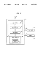
- FIG. 2 is a block diagram showing an exemplary computer graphics system 10 in which the anti-aliasing method and apparatus of the present invention can be employed.
- the computer graphics system 10 includes a host processor 12, a front end subsystem 14 and a frame buffer subsystem 20.
- the front end subsystem 14 receives primitive data from the host processor 12 over bus 11.
- each primitive is typically specified by x, y, z coordinate data, R,G,B color data, and texture data for certain portions of the primitives, such as the vertices when the primitive is a triangle.
- the front end subsystem 14 transforms the primitive data into edge equations for each primitive, identifying coordinates of each of the vertices of the primitive and slopes of the edges of the primitive, and transfers these edge equations to the frame buffer subsystem 20.
- the frame buffer subsystem 20 interpolates the edge equation data received from the front end subsystem 14 for each primitive to compute the pixel addresses, in display screen coordinates, and pixel color data that are used to represent each primitive on the display screen.
- the pixel color data includes bits identifying the red, green and blue color components of the pixel, and are stored in a frame buffer memory 22.
- the pixel color data are forwarded out of frame buffer memory 22 and through a Random Access Memory Digital to Analog Converter (RAMDAC) 27 which converts the binary color data stored in frame buffer memory 22 into analog red, green and blue signals for display on a display device (not shown).
- RAMDAC Random Access Memory Digital to Analog Converter
- front end subsystem 14 includes a host interface 16 and a three-dimensional (3-D) geometry accelerator 18.
- Host interface 16 receives the x, y, z vertex coordinate and color primitive data over bus 11 from host processor 12. This data is then provided from host interface 16 to geometry accelerator 18 over bus 11.
- Geometry accelerator 18 performs conventional geometry accelerator functions, such as three-dimensional transformation, lighting, clipping, and perspective divide operations, as well as generating edge equations in floating point format. In systems where a geometry accelerator is not provided, the edge equations are alternatively provided by the host processor. In the embodiment of FIG. 2, the edge equations are provided by geometry accelerator 18 over bus 18a to host interface 16 which forwards this edge equation data on bus 19 to the frame buffer subsystem 20.
- FIG. 3 a block diagram of a portion of the geometry accelerator 18 is shown including a transform unit 30, an edge generation unit 34 and a format conversion unit 36.
- the transform unit 30 receives, from the host interface 16 over bus 16A, coordinate and color data for each endpoint of each primitive.
- a triangle primitive for example, is represented by three vertex points, and thus will be represented by three vertex coordinates.
- the transform unit 30 includes a transform matrix 32 that is used to geometrically transform the input coordinates of primitive vertices into coordinates for representing the primitive on a display device.
- an example of the transform matrix 32 is shown including a number of rows and columns of matrix values a1-a4 . . . d1-d4.
- the matrix values are used to transform coordinates [x,y,z,w] of every into coordinates [x',y',z',w'] of a display device, where x, y are the pixel coordinates along the x and y axes, respectively, where z is the pixel coordinate along the z axis and thus provides visual depth information about the pixel, and where w is the pixel perspective, i.e., the size of the primitive relative to the size of the display.
- the matrix is device dependent, and thus the values in the matrix vary based on the number of pixels capable of being displayed on the display device.
- the transform matrix 32 may be used to scale a primitive by a scale value S by multiplying the appropriate matrix entries a1-a4, b1-b4, c1-c4 and d1-d4 by S using standard matrix multiplication techniques. This capability is provided in many graphics system to scale images for providing zoom capability.
- the transformed primitive data is forwarded to the edge generation unit 34 (FIG. 3).
- the edge generation unit 34 converts received primitive vertex data into edge equations representing the primitive. Referring now briefly to FIG. 4A, an example of some edge equations generated for a triangle are shown.
- the vertex coordinates received by the transform unit 30 from the host interface 16 are not yet scaled to account for the perspective of the primitive, i.e., the size of the primitive relative to the size of the display.
- the equations in group 40 are used to scale the x, y, and z coordinates of each of the vertexes v0, v1 and v2 by a perspective amount "wrecip" (which is equal to 1/w). Scaling by perspective allows for the scaling of an individual primitive. In contrast the transform matrix scales the entire image on the display.
- the equations in group 42 are then used to calculate the deltas of the edges.
- the deltas include length information identifying the overall length of the edge and color delta information identifying the change in color along the edge.
- the equations in group 44 are used to calculate the slopes of the edges of the primitive.
- edge assignments are also made. For example, when using triangles, the edge of the primitive with the longest y axis span is selected as edge one, the edge adjoining edge one at the lowest Y coordinate is edge two, and the remaining edge is edge three Based on the edge assignments, a direction value is generated, indicating an x axis direction proceeding from edge one to edge two. As described later herein, this direction value is used in one embodiment of the present invention by the frame buffer subsystem 20 for determining coordinates of pixels that are covered by the primitive.
- the edge equations and edge assignments are forwarded to format conversion unit 36, which re-formats the edge equations by performing a floating point to fixed point conversion to simplify later computations using the equations.
- the above edge equation data is forwarded out of the geometry accelerator 18 (FIG. 2) over bus 18a to host interface 16.
- the host interface 16 then forwards the edge equation data to the frame buffer subsystem 20.
- the frame buffer subsystem 20 includes two frame buffer controllers 24 and 26, each of which controls the display of one portion (22a, 22b) of the frame buffer memory 22 via control lines 23A and 23B, respectively.
- Frame buffer controller 24 controls the contents and display of data in the portion 22a of the frame buffer memory
- frame buffer controller 26 controls the contents and display of data in the portion 22b of frame buffer memory.
- two memory controllers are shown, other embodiments including, for example, one memory controller, or greater than two memory controllers may also be used.
- each frame buffer controller 24 and 26 handles primitive data destined for different addresses in the frame buffer memory 22, the remaining functionality of the controllers is substantially identical. As such, only one frame buffer controller will now be described in detail below.
- a frame buffer controller 24 in accordance with one embodiment of the present invention is shown including two functional units, a scan conversion unit 50 and a memory controller 60.
- the scan conversion unit 50 controls the translation of the edge equations into individual pixel data.
- the memory controller 60 controls the writing of the pixel data received from the scan conversion unit 50 into frame buffer memory 22.
- the memory controller includes logic 57 for performing anti-aliasing using data from the scan conversion unit 50 relating to multi-point sampling of primitives.
- the memory controller 60 is implemented as described in U.S. patent application Ser. No.
- the memory controller described in the above patent application describes an anti-aliasing method that uses subsample coverage information to determine color and perceived depth information (i.e, the z component) for each pixel to be rendered on the display device.
- the present invention may be used to provide the subsample coverage information that is used in the anti-aliasing method described in the '350 patent application.
- the method and apparatus for generating subsample information described herein can also be used with memory controllers implemented in other ways, and thus the present invention is not limited to the use with the '350 memory controller.
- the scan conversion unit 50 forwards pixel coordinate and color data to the memory controller.
- the scan conversion unit 50 also forwards a subsample mask to the memory controller.
- Each of the bits of the mask corresponds to one subsample of an associated pixel.
- the subsample mask is used during anti-aliasing to select an appropriate color value for the pixel.
- a portion of a display screen 70 is shown including a six row by six column pixel grid.
- the lines of the grid are drawn at integer values for both x and y coordinates in an x,y,z coordinate system of the display.
- Each of the horizontal lines x represents a scan line for the display.
- Scan line zero is at address (0,0)
- scan line one is at address (0,1) and so forth.
- a number of subsamples are included within each pixel and are shown as a number of dots labeled sub0-sub3 in pixel 73.
- the address, or origin, of each pixel in the x,y coordinate space is defined by the coordinates at the x,y intersections of the grid.
- Each pixel includes the subsamples within the pixel extending in an increasing x and increasing y direction to the next grid intersection.
- pixel (1,0) includes subsamples in grid block 75.
- the primitive of FIG. 6 is a triangle 74 drawn in a first color on a background of a second color. As described above with reference to FIG. 1, if the triangle 74 were rendered in aliased mode, each pixel where the pixel origin point is covered by the primitive would be rendered in the first color, while pixels where the pixel origin point is not covered by the primitive would be rendered in the second color. The resulting aliased primitive would be rendered with jagged edges, thus providing a sub-optimal image.
- the primitive may be rendered using an anti-aliased technique known as multi-point sampling.
- multi-point sampling each pixel is sampled at multiple coordinates within the pixel to provide a number of pixel subsamples.
- the number of subsamples of the pixel that are covered by the primitive is used in conjunction with other information (such as color data and z depth) to determine the color of the pixel.
- the pixel 75 at x,y coordinates (1,0) has two subsamples covered by the primitive.
- the color of the pixel would be a mixture of 50% of the primitive color, and 50% of the background color.
- Multi-point sampling is therefore useful in anti-aliasing because it provides information that is used to modulate color at the edges of a primitive to thereby reduce the appearance of jagged edges.
- Multi-point sampling is also useful for displaying objects that are smaller than the size of pixels. For example, if an object is smaller than the size of the pixel, and does not cover a single sample point of the pixel it is not displayed in aliased mode. Because multi-point sampling samples the image at multiple points within a display pixel defined by the pixel grid, sub-pixel sized objects can be sampled and the color of the pixel represented on the display.
- One component of multi-point sampling is the determination of how many subsamples in each pixel are covered by the primitive. The subsample information is determined during scan conversion and forwarded in the form of a mask to the memory controller which modulates the pixel color in accordance with the mask.
- mask information is produced by subdividing each scan line into a plurality of sub-scan lines, where sample points are located on sub-scan line boundaries, and then using hardware already provided in the system together with collection hardware of the invention to gather information about coverage of the subsamples within the pixel.
- the scan converter 50 including an edge stepper 52, collection logic 54 and a span stepper 56.
- the operation of each of these components is described below with reference to the portion of the illustrative image 70 shown in FIG. 6.
- Edge steppers and span steppers are commonly provided in graphics hardware for determining coordinates of pixels that are covered by primitives.
- the edge stepper 52, collection unit 54 and span steppers of one embodiment of the present invention can also provide mask information for use by the memory controller 60 during anti-aliasing operations.
- the edge stepper 52 receives the edge equations, such as those shown in FIG. 4A, from the graphics accelerator 18. Using the edge equations, the edge stepper incrementally steps along the edges of the primitive using a previously calculated edge point and pre-computed edge slope data to determine the edge coordinates of the primitive.
- the edge stepper can operate in either an aliased mode or an anti-aliased mode. In both modes, the basic method of operation is identical, it is only the input parameters to the edge stepper that differ. For purposes of explanation, an introduction to the edge stepping process will first be described with the edge stepper operating in conventional aliased mode. Then the modifications to the input parameters used when operating in anti-aliased mode will be described.
- the edges of the primitive 74 of FIG. 6 are indicated as edge one, edge two, and edge three.
- the edge stepper receives edge start and end information and slope information for the primitive.
- the edge stepper steps along each of the edges, gathering coordinate data for each of the pixels on each of the edges.
- the edge stepper ⁇ steps ⁇ from the start of edge one (where edge one crosses the scan line with the lowest y coordinate; i.e. point A in FIG. 6) to the next pixel coordinate of edge one until reaching the end of edge one, i.e., to vertex v1, essentially drawing a line between the two and determining what pixels in the image 70 are touched by edge one.
- FIG. 7 A block diagram of one illustrative embodiment of an edge stepper for implementing both aliased and anti-aliased modes of the present invention is shown in FIG. 7.
- the edge stepper logic uses a start y component and a stop y component received as part of the edge equation data from graphics accelerator 18.
- the start y component is the y address where edge one first crosses a scan line.
- the stop y component is the y component of vertex v1.
- the start y value i.e., the y component of point A in FIG. 6
- stop y value is 3.5.
- the start y component is fed through multiplexer 85 and stored in register 80 as Edge1 Y ⁇ 15:0>.
- the Edge1 Y component is the Y component that is forwarded out of the edge stepper 52 to the collection logic 54.
- the Edge1 Y component is forwarded to adder 86, where an increment value is added to the Edge1 Y component to provide the Next Y component.
- the increment value is provided by multiplexer 82, which selects one of a variety of values based on the status of an aliased bit, indicating whether the edge stepper is operating in aliased or anti-aliased mode, and a subgrid address which is described in more detail below.
- a +1 is added to the start y component to increment to the next scan line since each pixel y component is aligned on a scan line boundary.
- the remaining possible increment values, input to multiplexer 82, are provided for supporting operations in anti-aliasing mode, as explained in more detail below.
- the modifications to the edge stepper logic for supporting anti-aliased mode include multiplexer 82 and select control 84 and comparator 93 that will be explained later.
- a start x component is fed through multiplexer 95 and stored in a register 94.
- a slope x component is stored in a register 96.
- the start x and slope x components are received as part of the edge equation data from graphics accelerator 18.
- the start x component is the x component of edge one where edge one first crosses a scan line; i.e., the x coordinate corresponding to the start y coordinate (i.e., the x component of point A in FIG. 6).
- the slope x is the slope of edge one. In the example of FIG. 6, the start x value is the x address 2.2, and the slope x is 1.5.
- the start y component is forwarded through the multiplexer 85 and stored in register 80 as a current y value when a signal New Primitive is asserted.
- the New Primitive signal is asserted whenever a new primitive is forwarded to the edge stepper unit.
- the start x component is forwarded through multiplexer 95 when the New Primitive signal is asserted and stored in register 94, providing a current x value.
- the current x value is forwarded to an adder 99, which adds either a +1 or a -1 to the current x value, for reasons that will be described below.
- the current x value is also forwarded to a multiplexer 100.
- the multiplexer 100 selects between the current x value and the incremented (or decremented) x value depending upon the state of an Edge1 Status bit (described in more detail below), to provide an adjusted X ⁇ 31:16> value.
- the adjusted X value is forwarded to multiplexer 97, where either a shifted adjusted X value or a non-shifted adjusted X value, depending upon the status of an Aliased Bit (indicating operation in anti-aliased mode) as Edge1 X ⁇ 31:16>.
- the Edge1 X ⁇ 31:16> value is forwarded out of the edge stepper 52 to the collection logic 54.
- the current Y ⁇ 31:16> is forwarded to multiplexer 83, which selects either a shifted current Y value or a non-shifted current Y value as an Edge1 Y ⁇ 31:16> value depending upon the state of the Aliased Bit.
- the first Edge1 X, Edge1 Y component pair that is forwarded out of the edge stepper is (1,2).
- the current Y component is incremented by +1, and the result is fed back through multiplexer 85 and stored in register 88.
- the slope x is multiplied at multiplier 91 by the increment value provided from multiplexer 82 (which, for aliased mode is +1), added to the current X component at adder 98, and output as a Next X component
- the Next X component is forwarded through multiplexer 95, and loaded in register 94.
- a second coordinate pair of (2, 3) is generated for edge one.
- the current Y component is incremented by +1, the current X is incremented by the slope, and the results are loaded in registers 80 and 94, respectively, to provide Edge1 X, Edge1 Y coordinates of (3,5) for the next cycle.
- the process of incrementing continues until a comparator 92 determines that the Next Y value is greater than the value stored in the stop y register 90.
- the Next Y value is greater than the stop y value, edge stepping of the primitive is completed, and the signal End Primitive is asserted.
- the signals forwarded out of edge stepper 52 to collection logic 54 are the Edge1 X, Edge1 Y and End Primitive signals.
- edges two and three are treated as one edge (edge two/three) joined by a bend.
- the edge stepping logic for edge two/three is similar to that provided for edge one, with one exception.
- stepping is first done along edge two until the stop y value for edge two is encountered, and then stepping continues along edge three.
- edge stepping would occur along edge two, starting from edge two start x and start y coordinates (0.8,1) (indicated by point B in FIG. 6), and producing an edge two coordinate of (0.6,2).
- a compare similar to the compare done by comparator 92 in FIG.
- edge two Y coordinate is greater than the edge two stop Y value, stepping begins along edge three at an edge three start X coordinate.
- the first edge three coordinate that is generated is for scan line three, and is (2.7,3) (indicated by point C in FIG. 6). Stepping along edge three continues until the End Primitive signal is asserted by the Edge One edge stepper.
- edge 7 is modified in the edge two/three stepper by adding a multiplexer before the start x register 94 (to select between an edge two start x and an edge three start x) and adding a multiplexer before the stop Y register 90 (to select between an edge two stop Y and an edge one stop Y that is equal to the edge three stop y).
- a multiplexer is added before register 96, to select between and edge two slope and an edge three slope
- a multiplexer is added before start x register 95 to select between edge two and edge three start.
- An edge two/three coordinate may be generated at the same time that an edge one coordinate is generated for each scan line.
- Span stepper 56 steps along the x axis from an edge one x coordinate to an edge two/three x coordinate on each scan line covered by the primitive to determine the x,y coordinates of all of the pixels between edge one and edge two/three, and consequently all of the pixels covered by the primitive on that scan line.
- FIG. 1 is an example rendering of primitive 74 in aliased mode, where pixel coordinates have been generated using the edge stepping and span stepping operations described above. Since only the pixel coordinates are compared and generated during span stepping and edge stepping, only those pixels having their complete location covered by the primitive are ⁇ on ⁇ , the remaining pixels are ⁇ off ⁇ . In addition, because in aliased mode there is no modulation of color along the edges of the primitive, each pixel is either the background color or the primitive color. Thus, the aliased mode of operation is useful for rending primitives when high performance is desired. However, as shown in FIG. 1, aliased edges are often jagged and visually displeasing.
- Anti-aliasing using multi point sampling methods generally produces higher quality images, but at a reduced performance or higher hardware cost as compared to aliased images since multiple samples of each pixel are analyzed when determining the color of each pixel.
- the edge stepping and scan stepping are performed in aliased mode on a scan line granularity for providing pixel coordinate information to the memory controller.
- each pixel in anti-aliased mode, however, each pixel is apportioned into a number of sub-scan lines, and edge stepping is performed on a sub-scan line granularity.
- Subsamples are located on one or more sub-scan lines, and information about whether each of the subsamples is covered by the primitive is forwarded during anti-aliased mode to the memory controller by the span stepper.
- the same hardware is advantageously used for edge stepping and span stepping in both aliased and anti-aliased modes of operation.
- subsample information may be provided with minimal changes to the edge stepper and span stepper hardware.
- each scan line is subdivided into a plurality of sub-scan lines
- the image is first scaled by a predetermined amount such that each of the sub-scan lines falls on an integer address boundaries.
- the span and edge steppers need not deal with fractional pixel addresses, which simplifies the hardware.
- scaling need not be used, and sub-scan line coordinates can correspond to fractions of pixel coordinates.
- scaling is merely one embodiment for dividing a scan line into a number of sub-scan lines associated with sample coordinates within a pixel.
- the scaling of the image is performed in the transform unit 30 (FIG. 3) of the graphics accelerator chip 18 by multiplying the values in the transform matrix 32 (FIG. 3) by a desired scaling value.
- the scaling value is determined in part by the number of sample points that are desired for each pixel. In one embodiment of the invention, a scaling value of eight is used for accommodating placement of four sample points, although other scaling values and numbers of sample points may alternatively be used.
- the selection of the number of scaling points is influenced by the compute time required to process each of the samples on the sub-scan lines, and a relative improvement of the anti-aliased image over an aliased representation of the image.
- using four sample points per pixel has been found to provide significantly improved image quality over the aliased image while maintaining good performance.
- the scaling factor (e.g., eight) is greater than the number of sample points (e.g., four). This is advantageous in that it facilitates a non-regular placement of the sub-samples within the pixel.
- a non-regular placement means that the subsamples of each pixel may be placed at locations along the sub-scan lines such that the subsamples do not form a regular, grid-like pattern. Placing the subsamples at non-regular intervals along the sub-scan lines results in a reduction of the visual artifacts that are caused by ordered structures.
- the present invention is not limited, when scaling, to using a scaling factor that is greater than the number of samples.
- the scaling of an image by eight provides a number of other advantages. Because the scaling amount is a power of two, the multiplication step of scaling is easily accomplished by bit shifting. In addition, because a scaling size of eight was selected, three bits are used for determining a sub-scan line address. As will be described below, the x and y addresses used in one embodiment of the present invention each include a sixteen-bit integer portion such that the span and edge stepper hardware include registers capable of supporting sixteen bits of integer pixel coordinates. When three of the integer address bits are used as sub-scan line address bits during anti-aliasing, thirteen y address bits remain for addressing pixels within an image. Many applications, such as X Windows, require an image pixel address range of 8K, requiring thirteen bits. The use of a scaling factor of eight allows for maximizing the flexibility of subsample placement while still supporting applications such as X Windows for anti-aliasing operations.
- one embodiment of the present invention uses a scaling factor of eight with four subsamples, the present invention is not limited to these values. Rather, other scaling factors and other numbers of subsamples may alternatively be used. As described above, the selection of the scale value is dependent upon the available address space and the ease of computation. The selection of the numbers of subsamples is determined based upon a desired image quality and a desired performance.
- scaling technique may also be used to simplify mathematical calculations in other methods of antialiasing operations, where the mathematical calculations operate on at least one piece of information relating to the image and where the information includes a fractional components.
- the information may include sub-sample points, in multi-point sampling, but may also slope and edge equation parameters. Therefore, scaling of the image may be used to eliminate the fractional components of information, to thereby eliminate the need for complex floating point calculations.
- Edge stepping is performed on the scaled grid for anti-aliased images in a manner similar to that described with reference to FIG. 7 for aliased images.
- the only difference lies in how the Y axis address is interpreted; i.e., the Y axis address is a sub-scan line address in anti-aliased mode, as opposed to a scan line address in aliased mode.
- one embodiment of the X or Y address register comprising thirty-two bits stored in a sixteen.sixteen format.
- the most significant sixteen bits are integers
- the least significant sixteen bits represent a fractional portion of the address.
- register 101 One illustrative assignment of X or Y address register bits when operating in aliased mode is shown as register 101, where the integer portion of the X or Y address register 101a comprises sixteen bits of X or Y address information.
- register 103 An illustrative assignment of X or Y address register bits when operating in anti-aliased mode is shown as register 103, where the integer portion of the X or Y address includes a thirteen bit X or Y address 103a, and a three bit subgrid address 103b, where the three bit subgrid address encodes an address of one of the eight sub-scan lines of the pixel.
- Edge stepping in aliased mode uses the integer portion of the Y address register bits (31:16 shown in FIG. 9) as a basis for incremental stepping, while edge stepping in anti-aliased mode uses the same Y bits ⁇ 31:16> but, as will be shown, sub-grid address bits ⁇ 18:16> are used to control part of the anti-aliasing process.
- the illustrative embodiment only four subsamples are used. As a result, only the four sub-scan lines on which the subsamples lie (as shown in FIG. 8) are analyzed during the edge stepping process. Therefore, if the initial Y address subgrid field 103b is not a subgrid value that corresponds to a sub-scan line, the starting Y address is incremented to start at the next sub-scan line within the grid. For example, if the Y subgrid address field 103 was a 1, the start Y value for stepping is incremented by +2 to a 3, since that is the next sub-scan line having a sample point in the grid.
- the edge stepping hardware is also used for anti-aliased edge stepping is described.
- the start y value is forwarded through multiplexer 85, loaded into register 80 and stored as current Y ⁇ 31:16>.
- the current Y ⁇ 31:16> if forwarded to multiplexer 93, where either a shifted Y of a non-shifted current Y is provided as the Edge1 Y value depending upon the status of the Aliased Bit.
- bits ⁇ 18:16> are used in anti-aliased mode to provide a sub-scan line granularity for stepping.
- the integer portion of the Y component is formed from bits ⁇ 31:16> of the current Y value, and for aliased mode the integer portion of the Y component is formed from bits ⁇ 28:16> of the current Y value.
- the current Y value is also forwarded to the adder 86.
- an increment is also forwarded to the adder 86.
- the amount of the increment is determined by select control logic 81, and is based on the status of the Aliased Bit (which, as described above, indicates whether or not the graphics device is operating in aliased mode) and is further based on the initial subgrid address. As described above, if the subgrid address is not a sub-scan line address having a sample point, then the initial add operation adds the desired increment to go to the next sub-scan line. The increment needed for reaching the next sub-scan line address is then selected based upon the current sub-scan line address, and a delta y to the next sub-scan line address.
- the sub-scan line delta from sub-scan line zero to sub-scan line one is +3, from sub-scan line one to sub-scan line two is +2, from sub-scan line two to sub-scan line three is +2, and from sub-scan line three to sub-scan line 0 of the next pixel is a +1.
- the start y value is a 1
- the stop y value is greater than 8.0 (since the edge extends beyond the pixel 99)
- the start x value is a one
- the slope x is a one.
- the start y component is forwarded through multiplexer 85, stored in registers 80, and output as Edge1 Y to the collection logic 54.
- the start x component is forwarded through multiplexer 95 and stored in register 94 to provide a current x value.
- the current x value is forwarded through multiplexer 100 and provided as an adjusted X value, which is shifted in a manner similar to that described above with regard to the current Y component to provide an Edge1 X component for forwarding to collection logic 54.
- the current Y component of 1 is incremented by +2 to get to sub-scan line 3.
- the x coordinate at sub-scan line 3 is determined by multiplying the slope x value at multiplier 91 by the increment value of +2 and adding the results to the current X value at adder 98.
- the results from the adder 98 are fed back through multiplexer 95 and stored in register 94 to ultimately provide Edge1 Y and Edge1 X coordinates of (3, 3) for the next processing cycle of (3, 3).
- a comparator 93 compares the upper thirteen bits of the Next Y component from the adder 86 against the upper thirteen bits of the Edge1 Y value from register 80. As mentioned above, the upper thirteen bits represent the scan line component of the Y address. The two are unequal each time a scan line boundary has been crossed. When the two are unequal, or when the End Primitive signal is asserted, a New Y signal is asserted to indicate the start of processing of a new scan line. The New Y signal is forwarded to the collection logic 54.
- each edge sub-scan line coordinate x,y pair is generated, it is fed to collection logic 54 (FIG. 5). In addition, along with each edge sub-scan line coordinate x,y pair is sent the y subgrid address of the sub-scan line.
- the y subgrid address is used to distinguish between the x,y coordinate pairs that are on a valid sub-scanline (i.e., sub-scan lines zero, three, five or seven), and those that are not (i.e., those that fall on sub-scan lines one, two, four or six).
- the edge stepper 52 additionally includes status logic 84 for providing a status bit indicating whether a sub-sample on a sub-scan line is covered by an edge of the primitive.
- the status bit is determined according to the x coordinate of the edge as it crosses the sub-scan line, the x coordinate of the subsample on the respective sub-scan line, and the direction value received from the graphics accelerator 18.
- the direction value indicates what direction is stepped to go from edge one (the edge of the primitive with the largest Y axis span) to edge two (the edge that shares the uppermost Y vertex with edge one).
- a ⁇ 1 ⁇ value for the direction may indicate that edge one is on the left and that stepping is done from left to right
- a ⁇ 0 ⁇ may indicate that edge one is on the right, and that stepping is done from right to left.
- the direction value may be provided as a signal to the scan converter logic 50 on bus 19, or alternatively may be written to a register (not shown) of the scan conversion logic 50.
- the direction signal is encoded in the CMD field forwarded from graphics accelerator 18 to the scan conversion logic 50.
- Status logic 84 includes a comparator 89 coupled to receive the current x coordinate from register 94. The comparator also receives input from a multiplexer 87.
- the data inputs to the multiplexer are the x coordinates of the subsamples for each sub-scan line.
- the subsample coordinates in the illustrative embodiment are (0, 0), (7, 3), (3, 5) and (5, 7).
- the select inputs of the multiplexer 87 are controlled by the subgrid address bits ⁇ 18:16> of FIG. 9, which correspond to the sub-scan line address bits.
- the compare logic 89 also receives, as an input, the direction signal. If the direction signal indicates that the step direction is left to right, the compare logic asserts the status line for all sub-scan lines where the x coordinate of the edge is less than the subsample x coordinate (since all valid subsamples will be to the right of the edge). If the direction signal indicates that the step direction is right to left, the compare logic asserts the status line for all sub-scan lines where the x coordinate of the edge is greater than the subsample x coordinate, since all valid subsamples will be to the left of the edge.
- the edge stepping logic for edge two/three is substantially similar to that shown in FIG. 6 for edge one. One difference, however, is that an inverted value of the direction signal is input to the status logic 84 to ensure that the appropriate subsample pixels are selected for edge two/three.
- the Edge1 status signal is used to control multiplexer 100. If the current x coordinate does not cover a subsample, then the Edge1 status signal causes multiplexer 100 to select a modified current x value as the Edge1 X component that is forwarded to the collection logic.
- the modified x coordinate is the next sequential integer x coordinate in the direction of stepping relative to the current x coordinate.
- the current x coordinate is either incremented or decremented by 1 by the adder 99, depending upon the direction of stepping, if the compare operation performed by the status logic 84 indicates that the current x coordinate does not cover a sample point on the sub-scan line.
- the incrementing or decrementing of the x coordinate is provided to help identify specific types of primitives having a width that is less than the width of a pixel. Suffice it to say that, after adjustment of the current x coordinates for both edge one and edge two, it may occur that the distance between edge one and edge two/three is less than or equal to zero. The effect of having a distance less than or equal to zero between edges will be described later herein.
- Edge1 X, Edge1 Y, Edge23 X, New Y, and End Primitive signals are all forwarded to the collection logic 54 from the edge stepper 52.
- the Edge1 X, Edge23 X and Edge1 Y coordinates are forwarded after each sub-scan line calculation.
- the New Y signal is asserted when all the sub-scan lines in a given scan line have been processed.
- the End Primitive signal is asserted when the stepping of the primitive is complete.
- FIG. 10 a block diagram of one illustrative embodiment of the collection logic is shown including a control unit 104, a datapath 106, a Y coordinate buffer 108, an Edge1 X coordinate buffer 110, a length buffer 112, and plurality of other buffers 114, which store color, z and other data corresponding to each of the edges.
- Each of the buffers 108, 110, 112, and 114 includes two sets of four registers, where each four-register set stores a collection of sub-scan line edge coordinate data for the pixel most recently processed by the edge stepper. Data is received alternately by each half of the buffer, such that data may be input to one half of the buffer while data is being read out of the other half of the buffer.
- the control logic 104 receives the sub-scan line Y coordinate, New Y signal, End Primitive signal and a CMD field for identifying a function to be performed on the pixel data.
- the CMD field may be decoded to provide a mode status bit indicating operation in anti-aliased mode and a direction value indicating the direction of stepping.
- the control unit includes two functional units, a write control unit 104a and a read control unit 104b.
- the write control logic controls the writing of the received Edge1 Y and Edge1 X coordinate data into buffers 108 and 110, respectively.
- the write control logic controls the writing of a length value, corresponding to the Edge1 Y and Edge1 X values, into a length buffer 112.
- the Edge1 X and Edge23 X components are forwarded to the datapath 106.
- the datapath processes the Edge1 X and Edge23 X coordinates to provide a collected length value.
- the write control logic controls the subsequent writing of the collected length value from datapath 106 to buffer 112.
- the write control logic 104a also provides VALID ⁇ 3:0> signals and a New Group signal to the read control logic 104b.
- the New Group signal is asserted when either the New Y signal or the End Primitive signal is asserted by edge stepper 52.
- Each bit of the VALID signal corresponds to one of the four sub-scan lines, and indicates whether or not the sub-scan line was touched by the primitive.
- the VALID signals are encoded from the y subgrid address bits ⁇ 18:16>.
- the read control logic 104b includes a state machine that controls the transmission of command, coordinate, length and mask data to the span stepper (SS).
- the read control logic controls the transfer of SS CMD ⁇ 3:0> (from control unit 104), SS Y ⁇ 31:15> (from buffer 108), SS E1X ⁇ 15:0> (from buffer 110), SS Length signals (from buffer 112), and Color Z/out signals from buffer 114 to the span stepper 56.
- the write control logic 104a controls the accumulation of sub-scan line information in buffers 108, 110, 112 and 114
- the read control logic 104b controls the transfer of data from buffers 108, 110, 112 and 114 to the span stepper logic 58 (FIG. 5).
- the read control logic 104b additionally provides a MASK ⁇ 3:0> that is forwarded to the span stepper to identify the sub-samples covered by a pixel.
- a mux select signal is forwarded from the read control unit 104b to the datapath 106 to control the forwarding of the SS Length signal to the span stepper as described in more detail below.
- the datapath 106 similarly includes a collection unit 128 and a forward unit 130.
- the collection unit 128 receives the Edge1 X and Edge23 X coordinate data from the edge stepper 52.
- the Edge1 X and Edge23 X coordinates correspond to the edge one and edge two/three coordinates for the Y sub-scan line coordinate being processed.
- the collection unit 128 is able to determine, for each sub-scan line a length of the sub-scan line.
- the length of the sub-scan line is provided from the collection unit 128 as signals collected length, and stored in length buffer 112.
- the collection logic In addition to determining the length of each sub-scan line, the collection logic additionally determines a start and end of a ⁇ blasted region ⁇ of the sub-scan line being processed, where the blasted region identifies pixels within the sub-scan line having all of their samples covered by the primitive.
- a primitive 150 is shown.
- the pixels having all of their subsamples covered by the primitive 150 include pixels 153 and 154, which are referred to as ⁇ blasted ⁇ regions of the primitive.
- the blasted start value corresponds to the x,y coordinate of the pixel where the blasted region begins.
- the blasted length value corresponds to the number of pixels that are stepped along the sub-scanline in the blasted region.
- the edge one pixel x coordinates where the edge crosses the sub-scan lines 0, 1, 2 and 3 are 5, 4 and 5, respectively, where the pixel X coordinate of 4 on sub-scan line one is adjusted by the adjustment logic in FIG. 7.
- each valid sub-scan line coordinate is received from the write control logic 104a, it is compared against a previously stored sub-scan line x coordinate for the pixel to determine whether it is further in the direction of stepping than a previous sub-scan line x coordinate.
- the pixel x coordinate for sub-scan line 0 is a 5
- the pixel x coordinate for sub-scan line 1 is a 4.7
- the pixel x coordinate for sub-scan line 2 is a 5.5
- the pixel x coordinate for sub-scan line 3 is a 5.7.
- the pixel x coordinate of 4.7 is truncated, and selected as the blasted start value.
- a similar operation is followed using the coordinates of edge two/three to determine the blasted end value.
- FIG. 12 a flow diagram is shown illustrating the operation of collection unit 128 for providing the collected length value, the blasted start value and the blasted length value.
- the collected length value is generated for each sub-scan line.
- the blasted start and blasted length values are determined after all of the sub-scan lines are evaluated.
- the direction signal is evaluated. If the stepping direction is from right to left, then the processing path beginning with step 201a is selected. If the stepping direction is from left to right, then the processing path beginning with step 201b is selected.
- the processing paths are substantially similar, with the differences being in the type of comparisons made (i.e, greater than as opposed to less than) in each path. Thus, only the processing path beginning with step 201a is described below.
- blasted start and blasted end values are initialized. Depending upon the step direction, the blasted start value is set either to the Edge1 X coordinate, or to the Edge23 X coordinate of the sub-scan line, while the blasted end value is initialized as the opposite of the blasted start. Blasted start values are initialized in this manner to identify subsequent coordinates that are greater than (or less than) the initialized blasted start value (depending on the step direction), as will become more clear with the description below.
- the Edge1 X and Edge23 X coordinate for a given sub-scan line are received from write control logic 104a by the collection unit. 128.
- the Edge1 X coordinate is compared against the blasted start value. In the first pass through the steps of FIG. 12, the comparison is made against the blasted start value, while in subsequent passes the comparison is made against the blasted start value as updated during the process. If the Edge1 X coordinate is less than the blasted start value, and the direction of stepping is from right to left, then the Edge1 X value is saved as the blasted start value at step 209.
- a comparison is made to determine whether the Edge23 X coordinate is greater than the blasted end value for a right to left stepping direction, and if it is, then at step 207 the Edge23 X value is stored as the blasted end value.
- the total length of the sub-scan line is determined by subtracting the Edge23 X coordinate from the Edge1 X coordinate.
- the length value, calculated at step 211 is assigned to the collected length that is forwarded from the collection unit 128 and stored in length buffer 112.
- the status of the New Y signal, provided from the edge stepper 52 is checked at step 215.
- the New Y signal is asserted to indicate that the Y input coordinate has advanced to the next full scan line, and thus that all sub-scan lines have been processed for a given scan line, or that the primitive has finished being processed. If at step 215 the New Y signal is not asserted, the process resumes at step 202a, where a new Edge1 X and Edge23 X signal are received from edge stepper 52. If, at step 214, the New Y signal is asserted, a blasted length value is calculated by subtracting the blasted start from the blasted end, and the blasted start and blasted length values are forwarded to forward unit 130 of the datapath 106.
- the collected length value for the sub-scan line is accumulated in the buffer 110.
- the read control logic 104b starts the process of forwarding the stored Edge1 X, Edge1 Y, length, Mask, and CMD values for each sub-scan line stored in the buffers, to the span stepper 56.
- Edge1 X and Edge1 Y coordinate pair stored in the buffers 108 and 110 there are potentially three data transfers that may occur for the sub-scan line.
- the same Edge1 X and Edge1 Y values are forwarded, however, the Mask, CMD, and length values may differ as described below.
- the same Edge1 X coordinate is forwarded to the span stepper for each transfer, it will be seen below that this Edge1 X coordinate is only transferred to the memory controller 60 during the first transfer cycle per sub-scan line.
- the three data transfers are used to distinguish between the pixels on the sub-scan line before the blasted region, the pixels within the blasted region, and the pixels beyond the blasted region.
- the number of pixels before the blasted region is designated as length1
- the number of pixels within the blasted region is designated as length2, or blasted length
- the number of pixels beyond the blasted region is designated as length3.
- the length1 and length3 values may differ for each sub-scan line. For example, referring again to FIG. 11, sub-scan line 0 has a length1 value of one, since there is one pixel, at location (5,2), before the blasted region.
- Sub-scan line 0 has a length2 value of two, since there are two pixels within the blasted region.
- the length3 value for sub-scan line 0 is zero, since there are no pixels on sub-scan line zero beyond the blasted region.
- the length1, length2, and length3 values for sub-scan line 1 are zero, two and one, respectively.
- the length1, length2 and length3 values for sub-scan line 2 are one, two, and two, respectively, and the respective values for sub-scan line 3 are one, two, and three.
- the length1, length2 and length3 values are determined by the forward unit 130 (FIG. 10), and used to provide the appropriate length value for each of the three data transfer cycles of the sub-scan line on line SS length to the span stepper 56.
- FIG. 13 a block diagram of the forward unit 130 is shown including a first subtractor 220 for determining the length1 value in response to the SS E1X value, the blasted start value, and the direction signal.
- the SS E1X and length values are received from buffers 110 and 112, respectively, for each sub-scan line as controlled by the read control signal from read control logic 104b in the control unit 104.
- a second subtractor 222 calculates length3 by subtracting the sum of the blasted length and the length1 value from the length value received from buffer 112, which indicates the total length of the sub-scan line as calculated at step 211/212 of FIG. 12.
- the length1 and length3 values are forwarded to test logic 224 and 226, which test the values to determine if they are less than or equal to zero. If so, the signals len1 -- leq -- 0 and len3 -- leq -- 0 are respectively asserted, and forwarded to read control logic 104b, which uses them for controlling transfer of pixel data to the span stepper as will be described with regard to FIG. 15.
- the length value from buffer 112, is fed to test logic 225 to generate a length -- leq -- 0 signal that is forwarded to read control logic 104b for indicating whether it is less than or equal to zero.
- the blasted length value is also fed to tester 227 to generate a blasted -- leq -- 0 signal that is forwarded to read control logic 104b, which is also used for controlling the transfer of pixel data to the span stepper as will be described.
- the length1, length3, length, and blasted length values are forwarded to a multiplexer 228.
- the appropriate length value is forwarded as SS length to the span stepper by control logic 229 in response to the mux select ⁇ 2:0> signal received from read control logic 104b.
- the state machine includes four states, with each state dedicated to processing one of the sub-scan lines. Each state is entered only if the both corresponding VALID bit, received from write control logic 104a, indicates that the sub-scan line was touched by the primitive at the corresponding x, y coordinate, and if the length -- leq -- 0 signal for that sub-scan line is not asserted; i.e., as long as the overall length of the sub-scan line is greater than zero.
- VALID ⁇ 0> is checked to determine if sub-scan line 0 is valid. If so, at step 232, sub-scan line 0 is processed as will be described with regard to FIG. 15, and a Mask signal for sub-scan line 0 is defined as 0001. If sub-scan line 0 is not valid, or after processing sub-scan line 0, the process proceeds to step 234, where VALID ⁇ 1> and the length value for sub-scan line 1 checked to determine if sub-scan line 1 is valid. If so, at step 236, sub-scan line 1 is processed as described in FIG. 15, with a Mask value of 0010.
- a flow diagram illustrating the processing of each sub-scan line by the process of FIG. 14 in the read controller 104b begins when the New Group signal is asserted by the read control logic 104a, thus indicating that a new group of sub-scan lines is ready for processing.
- the status of the blasted -- leq -- 0 signal is checked to determine whether there is a blasted region for the set of sub-scan lines.
- step 254 the read control logic forwards a SS E1X value from buffer 110, a SS Y value from buffer 108, the SS length value from forward unit 130 (by asserting the appropriate mux select signal), the Mask corresponding to the processing state (232, 236, 240 or 244) of the control logic of read control 104b, the color/z data from buffer 114 and a SS CMD signal to the span stepper.
- the process continues at 250 by checking the len1 -- leq -- 0 signal received from the datapath 106. If the len1 -- leq -- 0 signal indicates that length1 is equal to zero, then no processing needs to be done for length1, and the process proceeds to step 255. However, if length1 does not equal 0, then the read control forwards a SS E1X value from buffer 110, a SS Y value from buffer 108, the SS length value from forward unit 130 (by asserting the appropriate mux select signal), the Mask corresponding to the processing state (232, 236, 240 or 244) of the control logic of read control 104b, the color/z data from buffer 114 and an SS CMD signal to the span stepper.
- the SS CMD signal has the encodings shown below in Table I:
- the SS CMD is used to allow the span stepper to select an appropriate X coordinate address to forward to the memory controller 60.
- the SS CMD signal helps the span stepper to identify the next pixel in the sub-scan line that needs to be processed, by directing it to use a previously accumulated E1X, color, Z and texture values, rather than the SS E1X, color Z and texture values provided by the collection logic.
- step 255 it is determined whether the mask equals 0001. Comparing the mask value against 0001 identifies whether or not the blasted region has already been processed, since the mask equals 0000 when the blasted region is processed at sub-scan line zero. According to one embodiment of the invention, the blasted region is only processed once for a group of sub-scan lines to advantageously reduce processing time for the pixel. If it has already been processed, the process proceeds to step 258. If the blasted region has not already been processed, then at step 256 the SS E1X, SS Y and SS length (equal to the blasted length) values are sent to the span stepper.
- the Mask value that is sent is set to 1111, thus indicating that all subsamples of the pixel are covered.
- the SS CMD that is sent is AA -- CMD -- 1, indicating that the span stepper should continue across the blasted region, starting at the previously incremented x coordinate (i.e., the x coordinate after processing of length1), and continue incrementing the x coordinate from that point.
- step 258 the len3 -- leq -- 0 signal from the forward unit is checked to determine if there are pixels in length3 of the sub-scanline to be evaluated. If length3 does not equal zero, then at step 260, the SS E1X, SS Y and SS length (equal to length3) values are sent to the span stepper.
- the Mask value that is sent is set according to the processing state of the process of FIG. 14 that calls the routine of FIG. 15.
- the SS CMD that is sent is AA -- CMD -- 2, indicating that the span stepper should continue incrementing the x coordinate starting at the x coordinate of the last pixel in the blasted region.
- commands that are sent to the span stepper which, for purposes of clarity, have not been described with regard to the flow diagram of FIG. 15.
- commands include the AA -- CMD -- 3, to skip the blasted region after starting with length1, the AA -- CMD -- 4, to start by accumulating the blasted region, and the AA -- CMD -- 5, to start by skipping the blasted region.
- AA -- CMD -- 3 is sent when length1 has been processed, the blasted region has already been processed for a preceding scan line, and length3 is not equal to zero.
- AA -- CMD -- 3 is sent when length1 is equal to zero, but there is a blasted region to process.
- AA -- CMD -- 5 is sent when length1 is equal to zero, and the blasted region has already been processed by a previous sub-scan line.
- Other commands may additionally be included to augment the functionality of the span stepper.
- each cycle of data forwarded from the collection logic to the span stepper includes an SS E1X, SS Y, SS Length, Mask and SS CMD value.
- the span stepper 56 uses the above signals to determine an address of each pixel that is covered by the primitive. To determine the address of each such pixel, the span stepper steps sequentially from one x coordinate to another along a sub-scan line for the total length of the sub-scan line. If the span stepper determines that a pixel is covered, an x and y coordinate for that pixel is forwarded to memory controller 60, with the pixel y coordinate address that is forwarded being the scan line address for that pixel.
- a four bit mask is forwarded to the memory controller 60, with the Mask value corresponding to the Mask signal that is sent from the collection logic.
- the span stepper 56 could potentially forward the same x,y coordinate to the memory controller four times, with a different bit in the mask being set for each x,y coordinate transfer.
- the identification of the blasted region provides a performance improvement when used with the embodiment of the invention wherein it is employed with a memory controller 60 implemented as described in the '350 patent application cited above.
- the memory controller 60 is able to process pixels having either only one bit set in their mask, or pixels having all of their bits set in the Mask. If a pixel has a Mask with two or three of the Mask bits set, the pixel coordinates are forwarded from the span stepper logic to the memory controller two or three times, once for each Mask bit set that is set. However, if all four bits are set, the pixel coordinates need only be forwarded once to the memory controller. More details regarding the performance benefits of identifying blasted regions will be provided below.
- the span stepper steps in given direction, from edge one to edge two, along the x coordinate axis as indicated by the direction signal.
- the direction signal is used to control a multiplexer 262 to provide either a +1 or a -1 value for the Inc/dec value signal.
- the SS CMD signal is forwarded from control unit 104 (FIG.
- state machine 263 decodes the SS CMD into the following signals: Load New Data for controlling the loading of the SS Y coordinate into register 266, Load New Mask for controlling the loading of the Mask into register 264, a signal Accumulate Blasted for controlling the incrementing of blasted count logic 270, and select ⁇ 1:0> signals that are used to control the selection of an x coordinate at a multiplexer 265.
- the span stepper operates generally as follows. When the SS E1X, SS Y and SS CMD signals are received at the span stepper, values for the control signals Load New Data, Load New Mask, Accumulate Blasted, and select ⁇ 1:0> are generated by the state machine 263.
- the select ⁇ 1:0> signals select one of four x coordinates input to multiplexer 265, and the multiplexer forwards the selected input to register 262 to be provided as the Pixel X coordinate to the memory controller 60.
- the four inputs to the multiplexer 265 include the SS E1X coordinate received from the collection logic 54, an After Blasted Start X coordinate, a Continue X coordinate and a Length3 X coordinate.
- the status of the SS CMD indicates which x-coordinate the span stepper uses as a starting coordinate for span stepping. For example, if the SS CMD decodes to AA -- CMD -- 0, indicating that the span stepping should begin at the start of length1, then the SS E1X coordinate is selected by multiplexer 265. If the SS CMD decodes to AA -- CMD -- 1, indicating span stepping should continue counting from the end of length1 across the blasted region, the Continue X coordinate is selected by multiplexer 265.
- the Continue X coordinate is also selected if the SS CMD decodes to AA -- CMD -- 2, indicating that counting continues from the end of the blasted region into length3. If the SS CMD decodes to AA -- CMD -- 3, indicating that the span stepper should start stepping after length1, but skip the blasted region, the After Blasted X coordinate is selected by multiplexer 265. If the SS CMD decodes to AA -- CMD -- 4, indicating that the span stepper should start stepping at the blasted region because the length1 is less than or equal to zero, the SS E1X coordinate is selected. If the SS CMD decodes to AA -- CMD -- 5, indicating that the span stepper should start stepping after the blasted region because the blasted region has previously been processed, the Length3 X coordinate is selected by multiplexer 265.
- the After Blasted Start X and Length3 X coordinates are provided by adders 267 and 269, respectively.
- the other input to adders 267 and 269 is a Delta X input.
- the Delta X input is provided by the blasted counter 270 and indicates the change in the x coordinate across the blasted region.
- the Delta X value is initialized by multiplexer 260, which forwards the Inc/Dec value received from multiplexer 262 to the register 261 for initialization purposes.
- the Accumulate Blasted signal is asserted (i.e., when the SS CMD equals AA -- CMD -- 1 or AA -- CMD -- 4), the multiplexer 260 switches to select the output from adder 259 for forwarding to the register 261.
- the adder increments (or decrements) the Delta X value for each cycle that a Pixel X coordinate is provided during processing of the blasted region.
- the Delta X value that is saved in register 261 represents the magnitude of change in value of the x coordinate as stepping proceeded across the blasted region.
- Accumulation logic similar to blasted counter 270 may also be provided for tracking and saving the total change of color and texture across a sub-scan line.
- the accumulation logic rather than providing a ⁇ 1 value to the input of the adder, would instead increment according to a delta color and delta texture parameter derived as part of the edge equation in software to determine a total change in color or texture across the sub-scan line.
- the operation of the span stepper 56 will now be described with reference to span stepping across scan line two of the example primitive 150 of FIG. 11.
- the SS E1X, SS Y coordinates are (5,2)
- the SS length value is a one
- the Mask is equal to 0001
- the SS CMD causes the SS E1X coordinate to be forwarded through multiplexer 265, loaded in register 262 and output as Pixel X coordinate.
- the Pixel X coordinate is forwarded to adder 267 and 268. Because the SS length value was a one, and one Pixel X coordinate was output, in the next cycle, the SS E1X, SS Y, Mask, SS length and SS CMD corresponding to the blasted region 152 are received.
- the received SS CMD for processing the blasted region of sub-scan line 0 equals AA -- CMD -- 1.
- the AA -- CMD -- 1 command causes the Load New Mask, Load New Data and Accumulate Blasted signals to be asserted.
- the AA -- CMD -- 1 value for the SS CMD causes the Continue X coordinate to be selected for stepping.
- the Continue X coordinate is obtained by decrementing the Pixel X coordinate (by adding a negative one value to the Pixel X coordinate since the step direction is right to left), stored in register 262 and output as Pixel X coordinate (4,2).
- the Mask stored in register 264 is equal to 1111, as described in step 256 of FIG. 15.
- the Continue X coordinate continues to be selected for each pixel in the blasted region.
- the Delta X value counts the magnitude of change of the x coordinate across the blasted region.
- a Pixel X,Y coordinate of (3,2) is generated, with a Mask of 1111.
- the stepping of the blasted region is complete and the stored Delta X value is equal to two.
- the select ⁇ 1:0> signals are set to select the Length3 X coordinate from adder.
- the first Pixel X,Y coordinates that are forwarded to the memory controller are (2,2).
- the Pixel Mask that is forwarded is indicated by the processing state of the process of FIG. 14 at step 236, and is thus a 0010 for this example.
- the Mask is forwarded either with only one bit set, or with all of the bits set.
- the Mask bits are forwarded in the above manner because the embodiment of the memory controller described in the above referenced patent application only has the capacity to process the pixel data either as discrete sub-pixels or as an entire pixel.
- the identification of the blasted region while improving the performance of the span stepper unit 58, also improves the overall memory performance by allowing those pixel coordinates that may be handled as full pixel updates to be identified and quickly transferred to memory for processing.
- the present invention is not limited to transferring subsample information as either a full four-bit mask, or as a single-bit mask. This effect is merely a constraint of the memory controller 60 used in one embodiment of the invention. When used with another memory controller that can support the receipt of mask data with greater than one but less than all bits set, the mask for each pixel could be sent directly from the span stepper logic in a single transfer.
Abstract
Description
              TABLE I
______________________________________
AA.sub.-- CMD.sub.-- 0
              Before Blasted Region
AA.sub.-- CMD.sub.-- 1
              Continue across blasted region
AA.sub.-- CMD.sub.-- 2
              Continue past blasted region
AA.sub.-- CMD.sub.-- 3
              Skip blasted region
AA.sub.-- CMD.sub.-- 4
              Start by accumulating blasted region
AA.sub.-- CMD.sub.-- 5
              Start by skipping blasted region
______________________________________
Claims (22)
Priority Applications (6)
| Application Number | Priority Date | Filing Date | Title |
|---|---|---|---|
| US08/887,441 US6057855A (en) | 1997-07-02 | 1997-07-02 | Method and apparatus for providing polygon pixel sub-sample information using incremental means |
| DE19827726A DE19827726B4 (en) | 1997-07-02 | 1998-06-22 | Method and apparatus for providing polygon pixel sub-sampling information using an incremental device |
| JP10180764A JPH1186007A (en) | 1997-07-02 | 1998-06-26 | Method for finding rate of pixel covered with primitive |
| GB9814268A GB2327178B (en) | 1997-07-02 | 1998-07-01 | Apparatus for providing polygon pixel sub-sample information using incremental means |
| GB0200840A GB2368763B (en) | 1997-07-02 | 1998-07-01 | Method for providing polygon pixel sub-sample information using incremental means |
| JP2003055630A JP2003271987A (en) | 1997-07-02 | 2003-03-03 | Method of determining percentage of pixel covered by primitive |
Applications Claiming Priority (1)
| Application Number | Priority Date | Filing Date | Title |
|---|---|---|---|
| US08/887,441 US6057855A (en) | 1997-07-02 | 1997-07-02 | Method and apparatus for providing polygon pixel sub-sample information using incremental means |
Publications (1)
| Publication Number | Publication Date |
|---|---|
| US6057855A true US6057855A (en) | 2000-05-02 |
Family
ID=25391134
Family Applications (1)
| Application Number | Title | Priority Date | Filing Date |
|---|---|---|---|
| US08/887,441 Expired - Fee Related US6057855A (en) | 1997-07-02 | 1997-07-02 | Method and apparatus for providing polygon pixel sub-sample information using incremental means |
Country Status (4)
| Country | Link |
|---|---|
| US (1) | US6057855A (en) |
| JP (2) | JPH1186007A (en) |
| DE (1) | DE19827726B4 (en) |
| GB (1) | GB2327178B (en) |
Cited By (120)
| Publication number | Priority date | Publication date | Assignee | Title |
|---|---|---|---|---|
| US6137918A (en) * | 1998-03-23 | 2000-10-24 | Xerox Corporation | Memory efficient method and apparatus to enable tagging of thin antialiased lines |
| US6167166A (en) * | 1998-03-23 | 2000-12-26 | Xerox Corporation | Method to enable the recognition and rendering of antialiased images |
| WO2001041069A1 (en) * | 1999-12-06 | 2001-06-07 | Nvidia | Method, apparatus and article of manufacture for a transform module in a graphics processor |
| US20010005209A1 (en) * | 1999-12-06 | 2001-06-28 | Lindholm John Erik | Method, apparatus and article of manufacture for a transform module in a graphics processor |
| US6377273B1 (en) * | 1998-11-04 | 2002-04-23 | Industrial Technology Research Institute | Fast area-coverage computing method for anti-aliasing in graphics |
| US6377274B1 (en) * | 1999-07-15 | 2002-04-23 | Intel Corporation | S-buffer anti-aliasing method |
| US20030095134A1 (en) * | 2000-11-12 | 2003-05-22 | Tuomi Mika Henrik | Method and apparatus for anti-aliasing for video applications |
| US6636232B2 (en) * | 2001-01-12 | 2003-10-21 | Hewlett-Packard Development Company, L.P. | Polygon anti-aliasing with any number of samples on an irregular sample grid using a hierarchical tiler |
| US20030206582A1 (en) * | 2002-05-02 | 2003-11-06 | Microsoft Corporation | 2-D transforms for image and video coding |
| US6650325B1 (en) * | 1999-12-06 | 2003-11-18 | Nvidia Corporation | Method, apparatus and article of manufacture for boustrophedonic rasterization |
| US20040012600A1 (en) * | 2002-03-22 | 2004-01-22 | Deering Michael F. | Scalable high performance 3d graphics |
| US6765575B1 (en) | 1999-12-06 | 2004-07-20 | Nvidia Corporation | Clip-less rasterization using line equation-based traversal |
| WO2004066358A2 (en) * | 2003-01-23 | 2004-08-05 | Photronics, Inc. | Binary half tone photomasks and microscopic three-dimensional devices and method of fabricating the same |
| US20040183816A1 (en) * | 2003-02-13 | 2004-09-23 | Leather Mark M. | Method and apparatus for sampling on a non-power-of-two pixel grid |
| US6809740B1 (en) * | 2000-07-26 | 2004-10-26 | Lexmark International, Inc. | Dithered quantization using neighborhood mask array to approximate interpolate |
| US20050007372A1 (en) * | 2003-06-26 | 2005-01-13 | Canon Kabushiki Kaisha | Rendering successive frames in a graphic object system |
| US6844880B1 (en) | 1999-12-06 | 2005-01-18 | Nvidia Corporation | System, method and computer program product for an improved programmable vertex processing model with instruction set |
| US20050017984A1 (en) * | 2003-06-26 | 2005-01-27 | Canon Kabushiki Kaisha | Optimising compositing calculations for a run of pixels |
| US20050035976A1 (en) * | 2003-06-26 | 2005-02-17 | Canon Kabushiki Kaisha | Antialiasing compositing in graphic object rendering |
| US6865301B1 (en) * | 2000-02-28 | 2005-03-08 | Adobe Systems Incorporated | Reducing aliasing artifacts when shaping a digital image |
| US20050141609A1 (en) * | 2001-09-18 | 2005-06-30 | Microsoft Corporation | Block transform and quantization for image and video coding |
| US20050256916A1 (en) * | 2004-05-14 | 2005-11-17 | Microsoft Corporation | Fast video codec transform implementations |
| US7006101B1 (en) | 2001-06-08 | 2006-02-28 | Nvidia Corporation | Graphics API with branching capabilities |
| US20060061590A1 (en) * | 2002-12-20 | 2006-03-23 | Tomas Akenine-Moller | Low-cost supersampling rasterization |
| US7046260B2 (en) * | 2000-12-20 | 2006-05-16 | Koninklijke Philips Electronics | Menu generating method and recording device for a record carrier |
| GB2420679A (en) * | 2004-11-29 | 2006-05-31 | Falanx Microsystems As | Rasterisation, storage, downsampling and rendering of graphical primitive data |
| US7119809B1 (en) | 2000-05-15 | 2006-10-10 | S3 Graphics Co., Ltd. | Parallel architecture for graphics primitive decomposition |
| US20060244748A1 (en) * | 2003-06-26 | 2006-11-02 | Canon Kabushiki Kaisha | Method for tracking depths in a scanline based raster image processor |
| US7170513B1 (en) | 1998-07-22 | 2007-01-30 | Nvidia Corporation | System and method for display list occlusion branching |
| US20070024639A1 (en) * | 2005-08-01 | 2007-02-01 | Luxology, Llc | Method of rendering pixel images from abstract datasets |
| US20070055967A1 (en) * | 1997-05-08 | 2007-03-08 | Poff Thomas C | Offload system, method, and computer program product for port-related processing |
| US20070081734A1 (en) * | 2005-10-07 | 2007-04-12 | Microsoft Corporation | Multimedia signal processing using fixed-point approximations of linear transforms |
| AU2004202826B2 (en) * | 2003-06-26 | 2007-09-06 | Canon Kabushiki Kaisha | Antialiasing Compositing in Graphic Object Rendering |
| US20080107356A1 (en) * | 2006-10-10 | 2008-05-08 | Kabushiki Kaisha Toshiba | Super-resolution device and method |
| US20080198163A1 (en) * | 2005-01-25 | 2008-08-21 | Sony Computer Entertainment Inc. | Drawing Method, Image Generating Device, And Electronic Information Apparatus |
| US20080198935A1 (en) * | 2007-02-21 | 2008-08-21 | Microsoft Corporation | Computational complexity and precision control in transform-based digital media codec |
| US20090051701A1 (en) * | 2005-03-14 | 2009-02-26 | Michael Fleming | Information layout |
| US20090195555A1 (en) * | 2008-01-31 | 2009-08-06 | Arm Norway As | Methods of and apparatus for processing computer graphics |
| US20090195552A1 (en) * | 2008-01-31 | 2009-08-06 | Arm Norway As | Methods of and apparatus for processing computer graphics |
| US7616202B1 (en) * | 2005-08-12 | 2009-11-10 | Nvidia Corporation | Compaction of z-only samples |
| US7697008B1 (en) | 1999-12-06 | 2010-04-13 | Nvidia Corporation | System, method and article of manufacture for a programmable processing model with instruction set |
| US20100110102A1 (en) * | 2008-10-24 | 2010-05-06 | Arm Limited | Methods of and apparatus for processing computer graphics |
| US8010082B2 (en) | 2004-10-20 | 2011-08-30 | Seven Networks, Inc. | Flexible billing architecture |
| US8064583B1 (en) | 2005-04-21 | 2011-11-22 | Seven Networks, Inc. | Multiple data store authentication |
| US8069166B2 (en) | 2005-08-01 | 2011-11-29 | Seven Networks, Inc. | Managing user-to-user contact with inferred presence information |
| US8078158B2 (en) | 2008-06-26 | 2011-12-13 | Seven Networks, Inc. | Provisioning applications for a mobile device |
| US8107921B2 (en) | 2008-01-11 | 2012-01-31 | Seven Networks, Inc. | Mobile virtual network operator |
| US8116214B2 (en) | 2004-12-03 | 2012-02-14 | Seven Networks, Inc. | Provisioning of e-mail settings for a mobile terminal |
| US8127342B2 (en) | 2002-01-08 | 2012-02-28 | Seven Networks, Inc. | Secure end-to-end transport through intermediary nodes |
| US8166164B1 (en) | 2010-11-01 | 2012-04-24 | Seven Networks, Inc. | Application and network-based long poll request detection and cacheability assessment therefor |
| US8190701B2 (en) | 2010-11-01 | 2012-05-29 | Seven Networks, Inc. | Cache defeat detection and caching of content addressed by identifiers intended to defeat cache |
| CN102486870A (en) * | 2010-12-01 | 2012-06-06 | 财团法人资讯工业策进会 | Drawing system and pixel updating method thereof |
| US20120229871A1 (en) * | 1997-06-09 | 2012-09-13 | Seiko Epson Corporation | Image Processing Apparatus, an Image Processing Method, A Medium on Which an Image Processing Control Program is Recorded, an Image Evaluation Device, an Image Evaluation Method and a Medium on Which an Image Evaluation Program is Recorded |
| US8269768B1 (en) | 1998-07-22 | 2012-09-18 | Nvidia Corporation | System, method and computer program product for updating a far clipping plane in association with a hierarchical depth buffer |
| US8316098B2 (en) | 2011-04-19 | 2012-11-20 | Seven Networks Inc. | Social caching for device resource sharing and management |
| CN101661732B (en) * | 2008-08-28 | 2012-11-21 | 夏普株式会社 | Data creating apparatus, drawing apparatus and controlling methods thereof, and recording media |
| CN101661733B (en) * | 2008-08-28 | 2012-11-21 | 夏普株式会社 | Data creating apparatus and drawing apparatus |
| US8326985B2 (en) | 2010-11-01 | 2012-12-04 | Seven Networks, Inc. | Distributed management of keep-alive message signaling for mobile network resource conservation and optimization |
| US8364181B2 (en) | 2007-12-10 | 2013-01-29 | Seven Networks, Inc. | Electronic-mail filtering for mobile devices |
| US8412675B2 (en) | 2005-08-01 | 2013-04-02 | Seven Networks, Inc. | Context aware data presentation |
| US8417823B2 (en) | 2010-11-22 | 2013-04-09 | Seven Network, Inc. | Aligning data transfer to optimize connections established for transmission over a wireless network |
| US8438633B1 (en) | 2005-04-21 | 2013-05-07 | Seven Networks, Inc. | Flexible real-time inbox access |
| US8468126B2 (en) | 2005-08-01 | 2013-06-18 | Seven Networks, Inc. | Publishing data in an information community |
| US8484314B2 (en) | 2010-11-01 | 2013-07-09 | Seven Networks, Inc. | Distributed caching in a wireless network of content delivered for a mobile application over a long-held request |
| US20130187956A1 (en) * | 2012-01-23 | 2013-07-25 | Walter R. Steiner | Method and system for reducing a polygon bounding box |
| US8621075B2 (en) | 2011-04-27 | 2013-12-31 | Seven Metworks, Inc. | Detecting and preserving state for satisfying application requests in a distributed proxy and cache system |
| US8693494B2 (en) | 2007-06-01 | 2014-04-08 | Seven Networks, Inc. | Polling |
| US8700728B2 (en) | 2010-11-01 | 2014-04-15 | Seven Networks, Inc. | Cache defeat detection and caching of content addressed by identifiers intended to defeat cache |
| US8750123B1 (en) | 2013-03-11 | 2014-06-10 | Seven Networks, Inc. | Mobile device equipped with mobile network congestion recognition to make intelligent decisions regarding connecting to an operator network |
| US8761756B2 (en) | 2005-06-21 | 2014-06-24 | Seven Networks International Oy | Maintaining an IP connection in a mobile network |
| US8774844B2 (en) | 2007-06-01 | 2014-07-08 | Seven Networks, Inc. | Integrated messaging |
| US8775631B2 (en) | 2012-07-13 | 2014-07-08 | Seven Networks, Inc. | Dynamic bandwidth adjustment for browsing or streaming activity in a wireless network based on prediction of user behavior when interacting with mobile applications |
| US8787947B2 (en) | 2008-06-18 | 2014-07-22 | Seven Networks, Inc. | Application discovery on mobile devices |
| US8793305B2 (en) | 2007-12-13 | 2014-07-29 | Seven Networks, Inc. | Content delivery to a mobile device from a content service |
| US8799410B2 (en) | 2008-01-28 | 2014-08-05 | Seven Networks, Inc. | System and method of a relay server for managing communications and notification between a mobile device and a web access server |
| US8805334B2 (en) | 2004-11-22 | 2014-08-12 | Seven Networks, Inc. | Maintaining mobile terminal information for secure communications |
| US8812695B2 (en) | 2012-04-09 | 2014-08-19 | Seven Networks, Inc. | Method and system for management of a virtual network connection without heartbeat messages |
| US8832228B2 (en) | 2011-04-27 | 2014-09-09 | Seven Networks, Inc. | System and method for making requests on behalf of a mobile device based on atomic processes for mobile network traffic relief |
| US8838783B2 (en) | 2010-07-26 | 2014-09-16 | Seven Networks, Inc. | Distributed caching for resource and mobile network traffic management |
| CN104050626A (en) * | 2013-03-15 | 2014-09-17 | 辉达公司 | Conservative rasterization of primitives using an error term |
| US20140267373A1 (en) * | 2013-03-15 | 2014-09-18 | Nvidia Corporation | Stencil then cover path rendering with shared edges |
| US8843153B2 (en) | 2010-11-01 | 2014-09-23 | Seven Networks, Inc. | Mobile traffic categorization and policy for network use optimization while preserving user experience |
| US8849902B2 (en) | 2008-01-25 | 2014-09-30 | Seven Networks, Inc. | System for providing policy based content service in a mobile network |
| US8861354B2 (en) | 2011-12-14 | 2014-10-14 | Seven Networks, Inc. | Hierarchies and categories for management and deployment of policies for distributed wireless traffic optimization |
| US8868753B2 (en) | 2011-12-06 | 2014-10-21 | Seven Networks, Inc. | System of redundantly clustered machines to provide failover mechanisms for mobile traffic management and network resource conservation |
| US8874761B2 (en) | 2013-01-25 | 2014-10-28 | Seven Networks, Inc. | Signaling optimization in a wireless network for traffic utilizing proprietary and non-proprietary protocols |
| US8886176B2 (en) | 2010-07-26 | 2014-11-11 | Seven Networks, Inc. | Mobile application traffic optimization |
| US8903954B2 (en) | 2010-11-22 | 2014-12-02 | Seven Networks, Inc. | Optimization of resource polling intervals to satisfy mobile device requests |
| US8909202B2 (en) | 2012-01-05 | 2014-12-09 | Seven Networks, Inc. | Detection and management of user interactions with foreground applications on a mobile device in distributed caching |
| US8909759B2 (en) | 2008-10-10 | 2014-12-09 | Seven Networks, Inc. | Bandwidth measurement |
| US8918503B2 (en) | 2011-12-06 | 2014-12-23 | Seven Networks, Inc. | Optimization of mobile traffic directed to private networks and operator configurability thereof |
| USRE45348E1 (en) | 2004-10-20 | 2015-01-20 | Seven Networks, Inc. | Method and apparatus for intercepting events in a communication system |
| US8984581B2 (en) | 2011-07-27 | 2015-03-17 | Seven Networks, Inc. | Monitoring mobile application activities for malicious traffic on a mobile device |
| US9002828B2 (en) | 2007-12-13 | 2015-04-07 | Seven Networks, Inc. | Predictive content delivery |
| US9002125B2 (en) | 2012-10-15 | 2015-04-07 | Nvidia Corporation | Z-plane compression with z-plane predictors |
| US9009250B2 (en) | 2011-12-07 | 2015-04-14 | Seven Networks, Inc. | Flexible and dynamic integration schemas of a traffic management system with various network operators for network traffic alleviation |
| US9021021B2 (en) | 2011-12-14 | 2015-04-28 | Seven Networks, Inc. | Mobile network reporting and usage analytics system and method aggregated using a distributed traffic optimization system |
| US9043731B2 (en) | 2010-03-30 | 2015-05-26 | Seven Networks, Inc. | 3D mobile user interface with configurable workspace management |
| US9043433B2 (en) | 2010-07-26 | 2015-05-26 | Seven Networks, Inc. | Mobile network traffic coordination across multiple applications |
| US9055102B2 (en) | 2006-02-27 | 2015-06-09 | Seven Networks, Inc. | Location-based operations and messaging |
| US9060032B2 (en) | 2010-11-01 | 2015-06-16 | Seven Networks, Inc. | Selective data compression by a distributed traffic management system to reduce mobile data traffic and signaling traffic |
| US9065765B2 (en) | 2013-07-22 | 2015-06-23 | Seven Networks, Inc. | Proxy server associated with a mobile carrier for enhancing mobile traffic management in a mobile network |
| US9077630B2 (en) | 2010-07-26 | 2015-07-07 | Seven Networks, Inc. | Distributed implementation of dynamic wireless traffic policy |
| US9105250B2 (en) | 2012-08-03 | 2015-08-11 | Nvidia Corporation | Coverage compaction |
| US9161258B2 (en) | 2012-10-24 | 2015-10-13 | Seven Networks, Llc | Optimized and selective management of policy deployment to mobile clients in a congested network to prevent further aggravation of network congestion |
| US9173128B2 (en) | 2011-12-07 | 2015-10-27 | Seven Networks, Llc | Radio-awareness of mobile device for sending server-side control signals using a wireless network optimized transport protocol |
| US9203864B2 (en) | 2012-02-02 | 2015-12-01 | Seven Networks, Llc | Dynamic categorization of applications for network access in a mobile network |
| US9241314B2 (en) | 2013-01-23 | 2016-01-19 | Seven Networks, Llc | Mobile device with application or context aware fast dormancy |
| US9275163B2 (en) | 2010-11-01 | 2016-03-01 | Seven Networks, Llc | Request and response characteristics based adaptation of distributed caching in a mobile network |
| US9307493B2 (en) | 2012-12-20 | 2016-04-05 | Seven Networks, Llc | Systems and methods for application management of mobile device radio state promotion and demotion |
| US9326189B2 (en) | 2012-02-03 | 2016-04-26 | Seven Networks, Llc | User as an end point for profiling and optimizing the delivery of content and data in a wireless network |
| US9325662B2 (en) | 2011-01-07 | 2016-04-26 | Seven Networks, Llc | System and method for reduction of mobile network traffic used for domain name system (DNS) queries |
| US9330196B2 (en) | 2010-11-01 | 2016-05-03 | Seven Networks, Llc | Wireless traffic management system cache optimization using http headers |
| US9578224B2 (en) | 2012-09-10 | 2017-02-21 | Nvidia Corporation | System and method for enhanced monoimaging |
| US9832095B2 (en) | 2011-12-14 | 2017-11-28 | Seven Networks, Llc | Operation modes for mobile traffic optimization and concurrent management of optimized and non-optimized traffic |
| US9829715B2 (en) | 2012-01-23 | 2017-11-28 | Nvidia Corporation | Eyewear device for transmitting signal and communication method thereof |
| US9906981B2 (en) | 2016-02-25 | 2018-02-27 | Nvidia Corporation | Method and system for dynamic regulation and control of Wi-Fi scans |
| US10263899B2 (en) | 2012-04-10 | 2019-04-16 | Seven Networks, Llc | Enhanced customer service for mobile carriers using real-time and historical mobile application and traffic or optimization data associated with mobile devices in a mobile network |
| US10536709B2 (en) | 2011-11-14 | 2020-01-14 | Nvidia Corporation | Prioritized compression for video |
| US10935788B2 (en) | 2014-01-24 | 2021-03-02 | Nvidia Corporation | Hybrid virtual 3D rendering approach to stereovision |
Families Citing this family (6)
| Publication number | Priority date | Publication date | Assignee | Title |
|---|---|---|---|---|
| WO2006129902A1 (en) * | 2005-06-03 | 2006-12-07 | Polidigm Co., Ltd. | Fast anti-aliasing method |
| JP4669334B2 (en) * | 2005-07-06 | 2011-04-13 | 株式会社ディジタルメディアプロフェッショナル | Edge multi-sampling hybrid anti-aliasing |
| US8269788B2 (en) * | 2005-11-15 | 2012-09-18 | Advanced Micro Devices Inc. | Vector graphics anti-aliasing |
| JP4855853B2 (en) * | 2006-07-05 | 2012-01-18 | 富士通株式会社 | Analysis device, computer control method, and model creation program |
| JP4766576B2 (en) * | 2009-03-25 | 2011-09-07 | 株式会社ソニー・コンピュータエンタテインメント | Drawing method, image generation apparatus, and electronic information device |
| KR101025475B1 (en) | 2009-06-17 | 2011-04-04 | 계명대학교 산학협력단 | Anti-aliasing Method and Apparatus |
Citations (10)
| Publication number | Priority date | Publication date | Assignee | Title |
|---|---|---|---|---|
| GB2243063A (en) * | 1990-02-28 | 1991-10-16 | Ricoh Kk | Variable sub pixel arrays for anti-aliasing |
| GB2245805A (en) * | 1990-06-29 | 1992-01-08 | Philips Electronic Associated | Generating an anti-aliased image |
| US5123085A (en) * | 1990-03-19 | 1992-06-16 | Sun Microsystems, Inc. | Method and apparatus for rendering anti-aliased polygons |
| US5381519A (en) * | 1987-12-04 | 1995-01-10 | Evans & Sutherland Computer Corp. | System for line interpolation for computer graphics displays |
| GB2285377A (en) * | 1993-12-28 | 1995-07-05 | Samsung Electronics Co Ltd | Method for generating a subpixel mask for anti-aliasing in a computer graphics system and apparatus thereof |
| JPH09102048A (en) * | 1995-10-03 | 1997-04-15 | Matsushita Electric Ind Co Ltd | Picture processor |
| US5668940A (en) * | 1994-08-19 | 1997-09-16 | Martin Marietta Corporation | Method and apparatus for anti-aliasing polygon edges in a computer imaging system |
| US5777629A (en) * | 1995-03-24 | 1998-07-07 | 3Dlabs Inc. Ltd. | Graphics subsystem with smart direct-memory-access operation |
| US5821949A (en) * | 1996-07-01 | 1998-10-13 | Sun Microsystems, Inc. | Three-dimensional graphics accelerator with direct data channels for improved performance |
| US5903276A (en) * | 1995-03-14 | 1999-05-11 | Ricoh Company, Ltd. | Image generating device with anti-aliasing function |
Family Cites Families (1)
| Publication number | Priority date | Publication date | Assignee | Title |
|---|---|---|---|---|
| DE69032932T2 (en) * | 1989-11-17 | 1999-09-16 | Digital Equipment Corp | System and method for genuine polygon drawing |
-
1997
- 1997-07-02 US US08/887,441 patent/US6057855A/en not_active Expired - Fee Related
-
1998
- 1998-06-22 DE DE19827726A patent/DE19827726B4/en not_active Expired - Fee Related
- 1998-06-26 JP JP10180764A patent/JPH1186007A/en active Pending
- 1998-07-01 GB GB9814268A patent/GB2327178B/en not_active Expired - Fee Related
-
2003
- 2003-03-03 JP JP2003055630A patent/JP2003271987A/en active Pending
Patent Citations (10)
| Publication number | Priority date | Publication date | Assignee | Title |
|---|---|---|---|---|
| US5381519A (en) * | 1987-12-04 | 1995-01-10 | Evans & Sutherland Computer Corp. | System for line interpolation for computer graphics displays |
| GB2243063A (en) * | 1990-02-28 | 1991-10-16 | Ricoh Kk | Variable sub pixel arrays for anti-aliasing |
| US5123085A (en) * | 1990-03-19 | 1992-06-16 | Sun Microsystems, Inc. | Method and apparatus for rendering anti-aliased polygons |
| GB2245805A (en) * | 1990-06-29 | 1992-01-08 | Philips Electronic Associated | Generating an anti-aliased image |
| GB2285377A (en) * | 1993-12-28 | 1995-07-05 | Samsung Electronics Co Ltd | Method for generating a subpixel mask for anti-aliasing in a computer graphics system and apparatus thereof |
| US5668940A (en) * | 1994-08-19 | 1997-09-16 | Martin Marietta Corporation | Method and apparatus for anti-aliasing polygon edges in a computer imaging system |
| US5903276A (en) * | 1995-03-14 | 1999-05-11 | Ricoh Company, Ltd. | Image generating device with anti-aliasing function |
| US5777629A (en) * | 1995-03-24 | 1998-07-07 | 3Dlabs Inc. Ltd. | Graphics subsystem with smart direct-memory-access operation |
| JPH09102048A (en) * | 1995-10-03 | 1997-04-15 | Matsushita Electric Ind Co Ltd | Picture processor |
| US5821949A (en) * | 1996-07-01 | 1998-10-13 | Sun Microsystems, Inc. | Three-dimensional graphics accelerator with direct data channels for improved performance |
Non-Patent Citations (4)
| Title |
|---|
| Anthony C. Barkans, "Hardware-Assisted Polygon Antialiasing", IEEE Computer Graphics and Applications 80-88 (Jan. 1991). |
| Anthony C. Barkans, Hardware Assisted Polygon Antialiasing , IEEE Computer Graphics and Applications 80 88 (Jan. 1991). * |
| Kurt Akeley, "Reality Engine Graphics", SIGGRAPH Computer Graphics Proceedings, Annual Conference Series 109-116 (Aug. 1993). |
| Kurt Akeley, Reality Engine Graphics , SIGGRAPH Computer Graphics Proceedings, Annual Conference Series 109 116 (Aug. 1993). * |
Cited By (225)
| Publication number | Priority date | Publication date | Assignee | Title |
|---|---|---|---|---|
| US20070055967A1 (en) * | 1997-05-08 | 2007-03-08 | Poff Thomas C | Offload system, method, and computer program product for port-related processing |
| US8867099B2 (en) * | 1997-06-09 | 2014-10-21 | Seiko Epson Corporation | Image processing apparatus, an image processing method, a medium on which an image processing control program is recorded, an image evaluation device, an image evaluation method and a medium on which an image evaluation program is recorded |
| US20120229871A1 (en) * | 1997-06-09 | 2012-09-13 | Seiko Epson Corporation | Image Processing Apparatus, an Image Processing Method, A Medium on Which an Image Processing Control Program is Recorded, an Image Evaluation Device, an Image Evaluation Method and a Medium on Which an Image Evaluation Program is Recorded |
| US6167166A (en) * | 1998-03-23 | 2000-12-26 | Xerox Corporation | Method to enable the recognition and rendering of antialiased images |
| US6137918A (en) * | 1998-03-23 | 2000-10-24 | Xerox Corporation | Memory efficient method and apparatus to enable tagging of thin antialiased lines |
| US8269768B1 (en) | 1998-07-22 | 2012-09-18 | Nvidia Corporation | System, method and computer program product for updating a far clipping plane in association with a hierarchical depth buffer |
| US7170513B1 (en) | 1998-07-22 | 2007-01-30 | Nvidia Corporation | System and method for display list occlusion branching |
| US6377273B1 (en) * | 1998-11-04 | 2002-04-23 | Industrial Technology Research Institute | Fast area-coverage computing method for anti-aliasing in graphics |
| US6377274B1 (en) * | 1999-07-15 | 2002-04-23 | Intel Corporation | S-buffer anti-aliasing method |
| US8264492B1 (en) | 1999-12-06 | 2012-09-11 | Nvidia Corporation | System, method and article of manufacture for a programmable processing model with instruction set |
| US7755636B1 (en) | 1999-12-06 | 2010-07-13 | Nvidia Corporation | System, method and article of manufacture for a programmable processing model with instruction set |
| US6650325B1 (en) * | 1999-12-06 | 2003-11-18 | Nvidia Corporation | Method, apparatus and article of manufacture for boustrophedonic rasterization |
| US7755634B1 (en) | 1999-12-06 | 2010-07-13 | Nvidia Corporation | System, method and computer program product for branching during programmable vertex processing |
| US6734874B2 (en) | 1999-12-06 | 2004-05-11 | Nvidia Corporation | Graphics processing unit with transform module capable of handling scalars and vectors |
| US6765575B1 (en) | 1999-12-06 | 2004-07-20 | Nvidia Corporation | Clip-less rasterization using line equation-based traversal |
| US7095414B2 (en) | 1999-12-06 | 2006-08-22 | Nvidia Corporation | Blending system and method in an integrated computer graphics pipeline |
| US20030112246A1 (en) * | 1999-12-06 | 2003-06-19 | Nvidia Corporation | Blending system and method in an integrated computer graphics pipeline |
| US7009607B2 (en) | 1999-12-06 | 2006-03-07 | Nvidia Corporation | Method, apparatus and article of manufacture for a transform module in a graphics processor |
| US7002588B1 (en) | 1999-12-06 | 2006-02-21 | Nvidia Corporation | System, method and computer program product for branching during programmable vertex processing |
| US8259122B1 (en) | 1999-12-06 | 2012-09-04 | Nvidia Corporation | System, method and article of manufacture for a programmable processing model with instruction set |
| US6844880B1 (en) | 1999-12-06 | 2005-01-18 | Nvidia Corporation | System, method and computer program product for an improved programmable vertex processing model with instruction set |
| WO2001041069A1 (en) * | 1999-12-06 | 2001-06-07 | Nvidia | Method, apparatus and article of manufacture for a transform module in a graphics processor |
| US7697008B1 (en) | 1999-12-06 | 2010-04-13 | Nvidia Corporation | System, method and article of manufacture for a programmable processing model with instruction set |
| US20010005209A1 (en) * | 1999-12-06 | 2001-06-28 | Lindholm John Erik | Method, apparatus and article of manufacture for a transform module in a graphics processor |
| US6353439B1 (en) * | 1999-12-06 | 2002-03-05 | Nvidia Corporation | System, method and computer program product for a blending operation in a transform module of a computer graphics pipeline |
| US6865301B1 (en) * | 2000-02-28 | 2005-03-08 | Adobe Systems Incorporated | Reducing aliasing artifacts when shaping a digital image |
| US7082223B1 (en) | 2000-02-28 | 2006-07-25 | Adobe Systems Incorporated | Reducing aliasing artifacts when shaping a digital image |
| US7119809B1 (en) | 2000-05-15 | 2006-10-10 | S3 Graphics Co., Ltd. | Parallel architecture for graphics primitive decomposition |
| US6809740B1 (en) * | 2000-07-26 | 2004-10-26 | Lexmark International, Inc. | Dithered quantization using neighborhood mask array to approximate interpolate |
| US7126611B1 (en) * | 2000-07-26 | 2006-10-24 | Lexmark International, Inc. | Dithered quantization using neighborhood mask array to approximate interpolate |
| US7489317B2 (en) * | 2000-11-12 | 2009-02-10 | Bitboys Oy, A Finnish Registered Co | Method and apparatus for anti-aliasing for video applications |
| US20030095134A1 (en) * | 2000-11-12 | 2003-05-22 | Tuomi Mika Henrik | Method and apparatus for anti-aliasing for video applications |
| US7061507B1 (en) * | 2000-11-12 | 2006-06-13 | Bitboys, Inc. | Antialiasing method and apparatus for video applications |
| US7046260B2 (en) * | 2000-12-20 | 2006-05-16 | Koninklijke Philips Electronics | Menu generating method and recording device for a record carrier |
| US6636232B2 (en) * | 2001-01-12 | 2003-10-21 | Hewlett-Packard Development Company, L.P. | Polygon anti-aliasing with any number of samples on an irregular sample grid using a hierarchical tiler |
| US7006101B1 (en) | 2001-06-08 | 2006-02-28 | Nvidia Corporation | Graphics API with branching capabilities |
| US20050141609A1 (en) * | 2001-09-18 | 2005-06-30 | Microsoft Corporation | Block transform and quantization for image and video coding |
| US20110116543A1 (en) * | 2001-09-18 | 2011-05-19 | Microsoft Corporation | Block transform and quantization for image and video coding |
| US8971405B2 (en) | 2001-09-18 | 2015-03-03 | Microsoft Technology Licensing, Llc | Block transform and quantization for image and video coding |
| US7881371B2 (en) | 2001-09-18 | 2011-02-01 | Microsoft Corporation | Block transform and quantization for image and video coding |
| US7839928B2 (en) | 2001-09-18 | 2010-11-23 | Microsoft Corporation | Block transform and quantization for image and video coding |
| US20050213659A1 (en) * | 2001-09-18 | 2005-09-29 | Microsoft Corporation | Block transform and quantization for image and video coding |
| US7773671B2 (en) | 2001-09-18 | 2010-08-10 | Microsoft Corporation | Block transform and quantization for image and video coding |
| US20050180503A1 (en) * | 2001-09-18 | 2005-08-18 | Microsoft Corporation | Block transform and quantization for image and video coding |
| US8989728B2 (en) | 2002-01-08 | 2015-03-24 | Seven Networks, Inc. | Connection architecture for a mobile network |
| US8127342B2 (en) | 2002-01-08 | 2012-02-28 | Seven Networks, Inc. | Secure end-to-end transport through intermediary nodes |
| US8811952B2 (en) | 2002-01-08 | 2014-08-19 | Seven Networks, Inc. | Mobile device power management in data synchronization over a mobile network with or without a trigger notification |
| US8549587B2 (en) | 2002-01-08 | 2013-10-01 | Seven Networks, Inc. | Secure end-to-end transport through intermediary nodes |
| US10019777B2 (en) | 2002-03-22 | 2018-07-10 | Gula Consulting Limited Liability Company | Scalable high performance 3D graphics |
| US20060092162A1 (en) * | 2002-03-22 | 2006-05-04 | Deering Michael F | Scalable high performance 3D graphics |
| US20110221742A1 (en) * | 2002-03-22 | 2011-09-15 | Michael F. Deering | Scalable High Performance 3D Graphics |
| US20040012600A1 (en) * | 2002-03-22 | 2004-01-22 | Deering Michael F. | Scalable high performance 3d graphics |
| US9478001B2 (en) | 2002-03-22 | 2016-10-25 | Gula Consulting Limited Liability Company | Scalable high performance 3D graphics |
| US7379067B2 (en) | 2002-03-22 | 2008-05-27 | Michael F. Deering | Scalable high performance 3D graphics |
| US8593468B2 (en) | 2002-03-22 | 2013-11-26 | Alandro Consulting Ny Llc | Scalable high performance 3D graphics |
| US20030206582A1 (en) * | 2002-05-02 | 2003-11-06 | Microsoft Corporation | 2-D transforms for image and video coding |
| US7242713B2 (en) * | 2002-05-02 | 2007-07-10 | Microsoft Corporation | 2-D transforms for image and video coding |
| US7495672B2 (en) | 2002-12-20 | 2009-02-24 | Telefonaktiebolaget Lm Ericsson (Publ) | Low-cost supersampling rasterization |
| US20060061590A1 (en) * | 2002-12-20 | 2006-03-23 | Tomas Akenine-Moller | Low-cost supersampling rasterization |
| WO2004066358A3 (en) * | 2003-01-23 | 2004-11-11 | Photronics Inc | Binary half tone photomasks and microscopic three-dimensional devices and method of fabricating the same |
| WO2004066358A2 (en) * | 2003-01-23 | 2004-08-05 | Photronics, Inc. | Binary half tone photomasks and microscopic three-dimensional devices and method of fabricating the same |
| US7280119B2 (en) * | 2003-02-13 | 2007-10-09 | Ati Technologies Inc. | Method and apparatus for sampling on a non-power-of-two pixel grid |
| US7545387B2 (en) * | 2003-02-13 | 2009-06-09 | Ati Technologies Ulc | Method and apparatus for sampling on a non-power-of-two pixel grid |
| US20070296733A1 (en) * | 2003-02-13 | 2007-12-27 | Ati Technologies Ulc | Method and apparatus for sampling on a non-power-of-two pixel grid |
| US20040183816A1 (en) * | 2003-02-13 | 2004-09-23 | Leather Mark M. | Method and apparatus for sampling on a non-power-of-two pixel grid |
| US7425955B2 (en) | 2003-06-26 | 2008-09-16 | Canon Kabushiki Kaisha | Method for tracking depths in a scanline based raster image processor |
| US7280120B2 (en) | 2003-06-26 | 2007-10-09 | Canon Kabushiki Kaisha | Compositing with a sub-pixel mask in graphic object rendering |
| US20050007372A1 (en) * | 2003-06-26 | 2005-01-13 | Canon Kabushiki Kaisha | Rendering successive frames in a graphic object system |
| US7292256B2 (en) | 2003-06-26 | 2007-11-06 | Canon Kabushiki Kaisha | Optimising compositing calculations for a run of pixels |
| US20060244748A1 (en) * | 2003-06-26 | 2006-11-02 | Canon Kabushiki Kaisha | Method for tracking depths in a scanline based raster image processor |
| AU2004202826B2 (en) * | 2003-06-26 | 2007-09-06 | Canon Kabushiki Kaisha | Antialiasing Compositing in Graphic Object Rendering |
| US20050017984A1 (en) * | 2003-06-26 | 2005-01-27 | Canon Kabushiki Kaisha | Optimising compositing calculations for a run of pixels |
| US7148897B2 (en) | 2003-06-26 | 2006-12-12 | Canon Kabushiki Kaisha | Rendering successive frames in a graphic object system |
| US20050035976A1 (en) * | 2003-06-26 | 2005-02-17 | Canon Kabushiki Kaisha | Antialiasing compositing in graphic object rendering |
| US7487193B2 (en) | 2004-05-14 | 2009-02-03 | Microsoft Corporation | Fast video codec transform implementations |
| US20050256916A1 (en) * | 2004-05-14 | 2005-11-17 | Microsoft Corporation | Fast video codec transform implementations |
| USRE45348E1 (en) | 2004-10-20 | 2015-01-20 | Seven Networks, Inc. | Method and apparatus for intercepting events in a communication system |
| US8010082B2 (en) | 2004-10-20 | 2011-08-30 | Seven Networks, Inc. | Flexible billing architecture |
| US8831561B2 (en) | 2004-10-20 | 2014-09-09 | Seven Networks, Inc | System and method for tracking billing events in a mobile wireless network for a network operator |
| US8805334B2 (en) | 2004-11-22 | 2014-08-12 | Seven Networks, Inc. | Maintaining mobile terminal information for secure communications |
| GB2420679B (en) * | 2004-11-29 | 2008-05-21 | Falanx Microsystems As | Processing of computer graphics |
| US8199146B2 (en) | 2004-11-29 | 2012-06-12 | Arm Norway As | Processing of computer graphics |
| US20080012878A1 (en) * | 2004-11-29 | 2008-01-17 | Jorn Nystad | Processing Of Computer Graphics |
| US7920139B2 (en) | 2004-11-29 | 2011-04-05 | Arm Norway As | Processing of computer graphics |
| GB2420679A (en) * | 2004-11-29 | 2006-05-31 | Falanx Microsystems As | Rasterisation, storage, downsampling and rendering of graphical primitive data |
| US20110148913A1 (en) * | 2004-11-29 | 2011-06-23 | Arm Norway As | Processing of computer graphics |
| CN101065784B (en) * | 2004-11-29 | 2011-11-30 | Arm挪威股份有限公司 | Processing of computer graphics |
| US8873411B2 (en) | 2004-12-03 | 2014-10-28 | Seven Networks, Inc. | Provisioning of e-mail settings for a mobile terminal |
| US8116214B2 (en) | 2004-12-03 | 2012-02-14 | Seven Networks, Inc. | Provisioning of e-mail settings for a mobile terminal |
| US20080198163A1 (en) * | 2005-01-25 | 2008-08-21 | Sony Computer Entertainment Inc. | Drawing Method, Image Generating Device, And Electronic Information Apparatus |
| US7884825B2 (en) | 2005-01-25 | 2011-02-08 | Sony Computer Entertainment Inc. | Drawing method, image generating device, and electronic information apparatus |
| US20090051701A1 (en) * | 2005-03-14 | 2009-02-26 | Michael Fleming | Information layout |
| US8561086B2 (en) | 2005-03-14 | 2013-10-15 | Seven Networks, Inc. | System and method for executing commands that are non-native to the native environment of a mobile device |
| US7877703B1 (en) | 2005-03-14 | 2011-01-25 | Seven Networks, Inc. | Intelligent rendering of information in a limited display environment |
| US20090051706A1 (en) * | 2005-03-14 | 2009-02-26 | Michael Fleming | Coordinate evaluation |
| US8209709B2 (en) | 2005-03-14 | 2012-06-26 | Seven Networks, Inc. | Cross-platform event engine |
| US7752633B1 (en) | 2005-03-14 | 2010-07-06 | Seven Networks, Inc. | Cross-platform event engine |
| US20090051704A1 (en) * | 2005-03-14 | 2009-02-26 | Michael Fleming | Object rendering from a base coordinate |
| US9047142B2 (en) | 2005-03-14 | 2015-06-02 | Seven Networks, Inc. | Intelligent rendering of information in a limited display environment |
| US8064583B1 (en) | 2005-04-21 | 2011-11-22 | Seven Networks, Inc. | Multiple data store authentication |
| US8839412B1 (en) | 2005-04-21 | 2014-09-16 | Seven Networks, Inc. | Flexible real-time inbox access |
| US8438633B1 (en) | 2005-04-21 | 2013-05-07 | Seven Networks, Inc. | Flexible real-time inbox access |
| US8761756B2 (en) | 2005-06-21 | 2014-06-24 | Seven Networks International Oy | Maintaining an IP connection in a mobile network |
| US20070024639A1 (en) * | 2005-08-01 | 2007-02-01 | Luxology, Llc | Method of rendering pixel images from abstract datasets |
| US7538779B2 (en) * | 2005-08-01 | 2009-05-26 | Luxology, Llc | Method of rendering pixel images from abstract datasets |
| US8069166B2 (en) | 2005-08-01 | 2011-11-29 | Seven Networks, Inc. | Managing user-to-user contact with inferred presence information |
| US8468126B2 (en) | 2005-08-01 | 2013-06-18 | Seven Networks, Inc. | Publishing data in an information community |
| US8412675B2 (en) | 2005-08-01 | 2013-04-02 | Seven Networks, Inc. | Context aware data presentation |
| US7616202B1 (en) * | 2005-08-12 | 2009-11-10 | Nvidia Corporation | Compaction of z-only samples |
| US7689052B2 (en) | 2005-10-07 | 2010-03-30 | Microsoft Corporation | Multimedia signal processing using fixed-point approximations of linear transforms |
| US20070081734A1 (en) * | 2005-10-07 | 2007-04-12 | Microsoft Corporation | Multimedia signal processing using fixed-point approximations of linear transforms |
| US9055102B2 (en) | 2006-02-27 | 2015-06-09 | Seven Networks, Inc. | Location-based operations and messaging |
| US8170376B2 (en) | 2006-10-10 | 2012-05-01 | Kabushiki Kaisha Toshiba | Super-resolution device and method |
| US8014632B2 (en) * | 2006-10-10 | 2011-09-06 | Kabushiki Kaisha Toshiba | Super-resolution device and method |
| US20080107356A1 (en) * | 2006-10-10 | 2008-05-08 | Kabushiki Kaisha Toshiba | Super-resolution device and method |
| US8942289B2 (en) | 2007-02-21 | 2015-01-27 | Microsoft Corporation | Computational complexity and precision control in transform-based digital media codec |
| US20080198935A1 (en) * | 2007-02-21 | 2008-08-21 | Microsoft Corporation | Computational complexity and precision control in transform-based digital media codec |
| US8693494B2 (en) | 2007-06-01 | 2014-04-08 | Seven Networks, Inc. | Polling |
| US8774844B2 (en) | 2007-06-01 | 2014-07-08 | Seven Networks, Inc. | Integrated messaging |
| US8805425B2 (en) | 2007-06-01 | 2014-08-12 | Seven Networks, Inc. | Integrated messaging |
| US8364181B2 (en) | 2007-12-10 | 2013-01-29 | Seven Networks, Inc. | Electronic-mail filtering for mobile devices |
| US8738050B2 (en) | 2007-12-10 | 2014-05-27 | Seven Networks, Inc. | Electronic-mail filtering for mobile devices |
| US8793305B2 (en) | 2007-12-13 | 2014-07-29 | Seven Networks, Inc. | Content delivery to a mobile device from a content service |
| US9002828B2 (en) | 2007-12-13 | 2015-04-07 | Seven Networks, Inc. | Predictive content delivery |
| US8107921B2 (en) | 2008-01-11 | 2012-01-31 | Seven Networks, Inc. | Mobile virtual network operator |
| US9712986B2 (en) | 2008-01-11 | 2017-07-18 | Seven Networks, Llc | Mobile device configured for communicating with another mobile device associated with an associated user |
| US8909192B2 (en) | 2008-01-11 | 2014-12-09 | Seven Networks, Inc. | Mobile virtual network operator |
| US8914002B2 (en) | 2008-01-11 | 2014-12-16 | Seven Networks, Inc. | System and method for providing a network service in a distributed fashion to a mobile device |
| US8849902B2 (en) | 2008-01-25 | 2014-09-30 | Seven Networks, Inc. | System for providing policy based content service in a mobile network |
| US8862657B2 (en) | 2008-01-25 | 2014-10-14 | Seven Networks, Inc. | Policy based content service |
| US8838744B2 (en) | 2008-01-28 | 2014-09-16 | Seven Networks, Inc. | Web-based access to data objects |
| US8799410B2 (en) | 2008-01-28 | 2014-08-05 | Seven Networks, Inc. | System and method of a relay server for managing communications and notification between a mobile device and a web access server |
| US8115783B2 (en) | 2008-01-31 | 2012-02-14 | Arm Norway As | Methods of and apparatus for processing computer graphics |
| US20090195555A1 (en) * | 2008-01-31 | 2009-08-06 | Arm Norway As | Methods of and apparatus for processing computer graphics |
| US20090195552A1 (en) * | 2008-01-31 | 2009-08-06 | Arm Norway As | Methods of and apparatus for processing computer graphics |
| US8044971B2 (en) | 2008-01-31 | 2011-10-25 | Arm Norway As | Methods of and apparatus for processing computer graphics |
| US8787947B2 (en) | 2008-06-18 | 2014-07-22 | Seven Networks, Inc. | Application discovery on mobile devices |
| US8078158B2 (en) | 2008-06-26 | 2011-12-13 | Seven Networks, Inc. | Provisioning applications for a mobile device |
| US8494510B2 (en) | 2008-06-26 | 2013-07-23 | Seven Networks, Inc. | Provisioning applications for a mobile device |
| CN101661733B (en) * | 2008-08-28 | 2012-11-21 | 夏普株式会社 | Data creating apparatus and drawing apparatus |
| CN101661732B (en) * | 2008-08-28 | 2012-11-21 | 夏普株式会社 | Data creating apparatus, drawing apparatus and controlling methods thereof, and recording media |
| US8909759B2 (en) | 2008-10-10 | 2014-12-09 | Seven Networks, Inc. | Bandwidth measurement |
| US20100110102A1 (en) * | 2008-10-24 | 2010-05-06 | Arm Limited | Methods of and apparatus for processing computer graphics |
| US9043731B2 (en) | 2010-03-30 | 2015-05-26 | Seven Networks, Inc. | 3D mobile user interface with configurable workspace management |
| US9043433B2 (en) | 2010-07-26 | 2015-05-26 | Seven Networks, Inc. | Mobile network traffic coordination across multiple applications |
| US9049179B2 (en) | 2010-07-26 | 2015-06-02 | Seven Networks, Inc. | Mobile network traffic coordination across multiple applications |
| US9077630B2 (en) | 2010-07-26 | 2015-07-07 | Seven Networks, Inc. | Distributed implementation of dynamic wireless traffic policy |
| US8838783B2 (en) | 2010-07-26 | 2014-09-16 | Seven Networks, Inc. | Distributed caching for resource and mobile network traffic management |
| US8886176B2 (en) | 2010-07-26 | 2014-11-11 | Seven Networks, Inc. | Mobile application traffic optimization |
| US9407713B2 (en) | 2010-07-26 | 2016-08-02 | Seven Networks, Llc | Mobile application traffic optimization |
| US8204953B2 (en) | 2010-11-01 | 2012-06-19 | Seven Networks, Inc. | Distributed system for cache defeat detection and caching of content addressed by identifiers intended to defeat cache |
| US8291076B2 (en) | 2010-11-01 | 2012-10-16 | Seven Networks, Inc. | Application and network-based long poll request detection and cacheability assessment therefor |
| US8484314B2 (en) | 2010-11-01 | 2013-07-09 | Seven Networks, Inc. | Distributed caching in a wireless network of content delivered for a mobile application over a long-held request |
| US8843153B2 (en) | 2010-11-01 | 2014-09-23 | Seven Networks, Inc. | Mobile traffic categorization and policy for network use optimization while preserving user experience |
| US9330196B2 (en) | 2010-11-01 | 2016-05-03 | Seven Networks, Llc | Wireless traffic management system cache optimization using http headers |
| US9275163B2 (en) | 2010-11-01 | 2016-03-01 | Seven Networks, Llc | Request and response characteristics based adaptation of distributed caching in a mobile network |
| US8326985B2 (en) | 2010-11-01 | 2012-12-04 | Seven Networks, Inc. | Distributed management of keep-alive message signaling for mobile network resource conservation and optimization |
| US9060032B2 (en) | 2010-11-01 | 2015-06-16 | Seven Networks, Inc. | Selective data compression by a distributed traffic management system to reduce mobile data traffic and signaling traffic |
| US8190701B2 (en) | 2010-11-01 | 2012-05-29 | Seven Networks, Inc. | Cache defeat detection and caching of content addressed by identifiers intended to defeat cache |
| US8166164B1 (en) | 2010-11-01 | 2012-04-24 | Seven Networks, Inc. | Application and network-based long poll request detection and cacheability assessment therefor |
| US8700728B2 (en) | 2010-11-01 | 2014-04-15 | Seven Networks, Inc. | Cache defeat detection and caching of content addressed by identifiers intended to defeat cache |
| US8782222B2 (en) | 2010-11-01 | 2014-07-15 | Seven Networks | Timing of keep-alive messages used in a system for mobile network resource conservation and optimization |
| US8966066B2 (en) | 2010-11-01 | 2015-02-24 | Seven Networks, Inc. | Application and network-based long poll request detection and cacheability assessment therefor |
| US9100873B2 (en) | 2010-11-22 | 2015-08-04 | Seven Networks, Inc. | Mobile network background traffic data management |
| US8903954B2 (en) | 2010-11-22 | 2014-12-02 | Seven Networks, Inc. | Optimization of resource polling intervals to satisfy mobile device requests |
| US8539040B2 (en) | 2010-11-22 | 2013-09-17 | Seven Networks, Inc. | Mobile network background traffic data management with optimized polling intervals |
| US8417823B2 (en) | 2010-11-22 | 2013-04-09 | Seven Network, Inc. | Aligning data transfer to optimize connections established for transmission over a wireless network |
| CN102486870B (en) * | 2010-12-01 | 2014-02-12 | 财团法人资讯工业策进会 | Drawing system and pixel updating method thereof |
| CN102486870A (en) * | 2010-12-01 | 2012-06-06 | 财团法人资讯工业策进会 | Drawing system and pixel updating method thereof |
| US9325662B2 (en) | 2011-01-07 | 2016-04-26 | Seven Networks, Llc | System and method for reduction of mobile network traffic used for domain name system (DNS) queries |
| US9300719B2 (en) | 2011-04-19 | 2016-03-29 | Seven Networks, Inc. | System and method for a mobile device to use physical storage of another device for caching |
| US8316098B2 (en) | 2011-04-19 | 2012-11-20 | Seven Networks Inc. | Social caching for device resource sharing and management |
| US8356080B2 (en) | 2011-04-19 | 2013-01-15 | Seven Networks, Inc. | System and method for a mobile device to use physical storage of another device for caching |
| US9084105B2 (en) | 2011-04-19 | 2015-07-14 | Seven Networks, Inc. | Device resources sharing for network resource conservation |
| US8832228B2 (en) | 2011-04-27 | 2014-09-09 | Seven Networks, Inc. | System and method for making requests on behalf of a mobile device based on atomic processes for mobile network traffic relief |
| US8621075B2 (en) | 2011-04-27 | 2013-12-31 | Seven Metworks, Inc. | Detecting and preserving state for satisfying application requests in a distributed proxy and cache system |
| US8635339B2 (en) | 2011-04-27 | 2014-01-21 | Seven Networks, Inc. | Cache state management on a mobile device to preserve user experience |
| US8984581B2 (en) | 2011-07-27 | 2015-03-17 | Seven Networks, Inc. | Monitoring mobile application activities for malicious traffic on a mobile device |
| US9239800B2 (en) | 2011-07-27 | 2016-01-19 | Seven Networks, Llc | Automatic generation and distribution of policy information regarding malicious mobile traffic in a wireless network |
| US10536709B2 (en) | 2011-11-14 | 2020-01-14 | Nvidia Corporation | Prioritized compression for video |
| US8868753B2 (en) | 2011-12-06 | 2014-10-21 | Seven Networks, Inc. | System of redundantly clustered machines to provide failover mechanisms for mobile traffic management and network resource conservation |
| US8918503B2 (en) | 2011-12-06 | 2014-12-23 | Seven Networks, Inc. | Optimization of mobile traffic directed to private networks and operator configurability thereof |
| US8977755B2 (en) | 2011-12-06 | 2015-03-10 | Seven Networks, Inc. | Mobile device and method to utilize the failover mechanism for fault tolerance provided for mobile traffic management and network/device resource conservation |
| US9277443B2 (en) | 2011-12-07 | 2016-03-01 | Seven Networks, Llc | Radio-awareness of mobile device for sending server-side control signals using a wireless network optimized transport protocol |
| US9009250B2 (en) | 2011-12-07 | 2015-04-14 | Seven Networks, Inc. | Flexible and dynamic integration schemas of a traffic management system with various network operators for network traffic alleviation |
| US9208123B2 (en) | 2011-12-07 | 2015-12-08 | Seven Networks, Llc | Mobile device having content caching mechanisms integrated with a network operator for traffic alleviation in a wireless network and methods therefor |
| US9173128B2 (en) | 2011-12-07 | 2015-10-27 | Seven Networks, Llc | Radio-awareness of mobile device for sending server-side control signals using a wireless network optimized transport protocol |
| US9021021B2 (en) | 2011-12-14 | 2015-04-28 | Seven Networks, Inc. | Mobile network reporting and usage analytics system and method aggregated using a distributed traffic optimization system |
| US8861354B2 (en) | 2011-12-14 | 2014-10-14 | Seven Networks, Inc. | Hierarchies and categories for management and deployment of policies for distributed wireless traffic optimization |
| US9832095B2 (en) | 2011-12-14 | 2017-11-28 | Seven Networks, Llc | Operation modes for mobile traffic optimization and concurrent management of optimized and non-optimized traffic |
| US9131397B2 (en) | 2012-01-05 | 2015-09-08 | Seven Networks, Inc. | Managing cache to prevent overloading of a wireless network due to user activity |
| US8909202B2 (en) | 2012-01-05 | 2014-12-09 | Seven Networks, Inc. | Detection and management of user interactions with foreground applications on a mobile device in distributed caching |
| US20130187956A1 (en) * | 2012-01-23 | 2013-07-25 | Walter R. Steiner | Method and system for reducing a polygon bounding box |
| US9633458B2 (en) * | 2012-01-23 | 2017-04-25 | Nvidia Corporation | Method and system for reducing a polygon bounding box |
| US9829715B2 (en) | 2012-01-23 | 2017-11-28 | Nvidia Corporation | Eyewear device for transmitting signal and communication method thereof |
| US9203864B2 (en) | 2012-02-02 | 2015-12-01 | Seven Networks, Llc | Dynamic categorization of applications for network access in a mobile network |
| US9326189B2 (en) | 2012-02-03 | 2016-04-26 | Seven Networks, Llc | User as an end point for profiling and optimizing the delivery of content and data in a wireless network |
| US8812695B2 (en) | 2012-04-09 | 2014-08-19 | Seven Networks, Inc. | Method and system for management of a virtual network connection without heartbeat messages |
| US10263899B2 (en) | 2012-04-10 | 2019-04-16 | Seven Networks, Llc | Enhanced customer service for mobile carriers using real-time and historical mobile application and traffic or optimization data associated with mobile devices in a mobile network |
| US8775631B2 (en) | 2012-07-13 | 2014-07-08 | Seven Networks, Inc. | Dynamic bandwidth adjustment for browsing or streaming activity in a wireless network based on prediction of user behavior when interacting with mobile applications |
| US9105250B2 (en) | 2012-08-03 | 2015-08-11 | Nvidia Corporation | Coverage compaction |
| US9578224B2 (en) | 2012-09-10 | 2017-02-21 | Nvidia Corporation | System and method for enhanced monoimaging |
| US9002125B2 (en) | 2012-10-15 | 2015-04-07 | Nvidia Corporation | Z-plane compression with z-plane predictors |
| US9161258B2 (en) | 2012-10-24 | 2015-10-13 | Seven Networks, Llc | Optimized and selective management of policy deployment to mobile clients in a congested network to prevent further aggravation of network congestion |
| US9307493B2 (en) | 2012-12-20 | 2016-04-05 | Seven Networks, Llc | Systems and methods for application management of mobile device radio state promotion and demotion |
| US9271238B2 (en) | 2013-01-23 | 2016-02-23 | Seven Networks, Llc | Application or context aware fast dormancy |
| US9241314B2 (en) | 2013-01-23 | 2016-01-19 | Seven Networks, Llc | Mobile device with application or context aware fast dormancy |
| US8874761B2 (en) | 2013-01-25 | 2014-10-28 | Seven Networks, Inc. | Signaling optimization in a wireless network for traffic utilizing proprietary and non-proprietary protocols |
| US8750123B1 (en) | 2013-03-11 | 2014-06-10 | Seven Networks, Inc. | Mobile device equipped with mobile network congestion recognition to make intelligent decisions regarding connecting to an operator network |
| US20140267374A1 (en) * | 2013-03-15 | 2014-09-18 | Nvidia Corporation | Stencil then cover path rendering with shared edges |
| US9466115B2 (en) * | 2013-03-15 | 2016-10-11 | Nvidia Corporation | Stencil then cover path rendering with shared edges |
| US20170024897A1 (en) * | 2013-03-15 | 2017-01-26 | Nvidia Corporation | Stencil-then-cover path rendering with shared edges |
| US9342891B2 (en) * | 2013-03-15 | 2016-05-17 | Nvidia Corporation | Stencil then cover path rendering with shared edges |
| TWI552109B (en) * | 2013-03-15 | 2016-10-01 | 輝達公司 | A method, a non-transitory computer-readable storage medium and a system for conservative rasterization of primitives using an error term |
| US9633469B2 (en) * | 2013-03-15 | 2017-04-25 | Nvidia Corporation | Conservative rasterization of primitives using an error term |
| US9418437B2 (en) * | 2013-03-15 | 2016-08-16 | Nvidia Corporation | Stencil then cover path rendering with shared edges |
| US20140267373A1 (en) * | 2013-03-15 | 2014-09-18 | Nvidia Corporation | Stencil then cover path rendering with shared edges |
| US20140267238A1 (en) * | 2013-03-15 | 2014-09-18 | Nvidia Corporation | Conservative rasterization of primitives using an error term |
| CN104050626B (en) * | 2013-03-15 | 2018-01-05 | 辉达公司 | For the method, system and storage medium for rasterizing primitive |
| CN104050626A (en) * | 2013-03-15 | 2014-09-17 | 辉达公司 | Conservative rasterization of primitives using an error term |
| US20140267375A1 (en) * | 2013-03-15 | 2014-09-18 | Nvidia Corporation | Stencil then cover path rendering with shared edges |
| US10083514B2 (en) * | 2013-03-15 | 2018-09-25 | Nvidia Corporation | Stencil-then-cover path rendering with shared edges |
| US9065765B2 (en) | 2013-07-22 | 2015-06-23 | Seven Networks, Inc. | Proxy server associated with a mobile carrier for enhancing mobile traffic management in a mobile network |
| US10935788B2 (en) | 2014-01-24 | 2021-03-02 | Nvidia Corporation | Hybrid virtual 3D rendering approach to stereovision |
| US9906981B2 (en) | 2016-02-25 | 2018-02-27 | Nvidia Corporation | Method and system for dynamic regulation and control of Wi-Fi scans |
Also Published As
| Publication number | Publication date |
|---|---|
| JPH1186007A (en) | 1999-03-30 |
| GB2327178A (en) | 1999-01-13 |
| DE19827726B4 (en) | 2005-02-24 |
| GB9814268D0 (en) | 1998-09-02 |
| GB2327178B (en) | 2002-03-20 |
| DE19827726A1 (en) | 1999-01-07 |
| JP2003271987A (en) | 2003-09-26 |
Similar Documents
| Publication | Publication Date | Title |
|---|---|---|
| US6057855A (en) | Method and apparatus for providing polygon pixel sub-sample information using incremental means | |
| EP0430501B1 (en) | System and method for drawing antialiased polygons | |
| US6914610B2 (en) | Graphics primitive size estimation and subdivision for use with a texture accumulation buffer | |
| US6459428B1 (en) | Programmable sample filtering for image rendering | |
| US6545686B1 (en) | Cache memory and method for use in generating computer graphics texture | |
| US6680735B1 (en) | Method for correcting gradients of irregular spaced graphic data | |
| US6795080B2 (en) | Batch processing of primitives for use with a texture accumulation buffer | |
| US6275235B1 (en) | High precision texture wrapping method and device | |
| US5519823A (en) | Apparatus for rendering antialiased vectors | |
| US6535220B2 (en) | Static and dynamic video resizing | |
| US6292192B1 (en) | System and method for the direct rendering of curve bounded objects | |
| US7106352B2 (en) | Automatic gain control, brightness compression, and super-intensity samples | |
| US5930407A (en) | System and method for efficiently generating cubic coefficients in a computer graphics system | |
| US5604852A (en) | Method and apparatus for displaying a parametric curve on a video display | |
| US6731300B2 (en) | Efficient anti-aliased dot rasterization | |
| US20060250407A1 (en) | Texture filtering using a programmable table filter to improve computer graphics performmance | |
| US6778188B2 (en) | Reconfigurable hardware filter for texture mapping and image processing | |
| US6181347B1 (en) | Selectable mode smoothing texture filter for computer graphics | |
| US6914609B2 (en) | Multiple scan line sample filtering | |
| US20030174133A1 (en) | Method for reduction of possible renderable graphics primitive shapes for rasterization | |
| US6130674A (en) | Dynamically selectable texture filter for computer graphics | |
| US6867778B2 (en) | End point value correction when traversing an edge using a quantized slope value | |
| EP1058912B1 (en) | Subsampled texture edge antialiasing | |
| US6943791B2 (en) | Z-slope test to optimize sample throughput | |
| GB2368763A (en) | Determining coverage of a pixel by a primitive |
Legal Events
| Date | Code | Title | Description |
|---|---|---|---|
| AS | Assignment |
Owner name: HEWLETT-PACKARD COMPANY, CALIFORNIA Free format text: ASSIGNMENT OF ASSIGNORS INTEREST;ASSIGNOR:BARKANS, ANTHONY;REEL/FRAME:008805/0200 Effective date: 19970618 |
|
| AS | Assignment |
Owner name: SAMSUNG ELECTRONICS CO., LTD., KOREA, REPUBLIC OF Free format text: ASSIGNMENT OF ASSIGNORS INTEREST;ASSIGNORS:SHIM, DA-HYUN;LEE, JUN-SUNG;REEL/FRAME:008906/0752 Effective date: 19971128 |
|
| AS | Assignment |
Owner name: HEWLETT-PACKARD COMPANY, COLORADO Free format text: MERGER;ASSIGNOR:HEWLETT-PACKARD COMPANY;REEL/FRAME:011523/0469 Effective date: 19980520 |
|
| CC | Certificate of correction | ||
| FPAY | Fee payment |
Year of fee payment: 4 |
|
| FEPP | Fee payment procedure |
Free format text: PAYOR NUMBER ASSIGNED (ORIGINAL EVENT CODE: ASPN); ENTITY STATUS OF PATENT OWNER: LARGE ENTITY |
|
| FPAY | Fee payment |
Year of fee payment: 8 |
|
| AS | Assignment |
Owner name: HEWLETT-PACKARD DEVELOPMENT COMPANY, L.P., TEXAS Free format text: ASSIGNMENT OF ASSIGNORS INTEREST;ASSIGNOR:HEWLETT-PACKARD COMPANY;REEL/FRAME:026945/0699 Effective date: 20030131 |
|
| REMI | Maintenance fee reminder mailed | ||
| LAPS | Lapse for failure to pay maintenance fees | ||
| STCH | Information on status: patent discontinuation |
Free format text: PATENT EXPIRED DUE TO NONPAYMENT OF MAINTENANCE FEES UNDER 37 CFR 1.362 |
|
| FP | Lapsed due to failure to pay maintenance fee |
Effective date: 20120502 |