US6080672A - Self-aligned contact formation for semiconductor devices - Google Patents
Self-aligned contact formation for semiconductor devices Download PDFInfo
- Publication number
- US6080672A US6080672A US08/915,386 US91538697A US6080672A US 6080672 A US6080672 A US 6080672A US 91538697 A US91538697 A US 91538697A US 6080672 A US6080672 A US 6080672A
- Authority
- US
- United States
- Prior art keywords
- gate
- forming
- dram
- insulating film
- spacer
- Prior art date
- Legal status (The legal status is an assumption and is not a legal conclusion. Google has not performed a legal analysis and makes no representation as to the accuracy of the status listed.)
- Expired - Lifetime
Links
Images


Classifications
-
- H—ELECTRICITY
- H01—ELECTRIC ELEMENTS
- H01L—SEMICONDUCTOR DEVICES NOT COVERED BY CLASS H10
- H01L21/00—Processes or apparatus adapted for the manufacture or treatment of semiconductor or solid state devices or of parts thereof
- H01L21/70—Manufacture or treatment of devices consisting of a plurality of solid state components formed in or on a common substrate or of parts thereof; Manufacture of integrated circuit devices or of parts thereof
- H01L21/77—Manufacture or treatment of devices consisting of a plurality of solid state components or integrated circuits formed in, or on, a common substrate
- H01L21/78—Manufacture or treatment of devices consisting of a plurality of solid state components or integrated circuits formed in, or on, a common substrate with subsequent division of the substrate into plural individual devices
- H01L21/82—Manufacture or treatment of devices consisting of a plurality of solid state components or integrated circuits formed in, or on, a common substrate with subsequent division of the substrate into plural individual devices to produce devices, e.g. integrated circuits, each consisting of a plurality of components
- H01L21/822—Manufacture or treatment of devices consisting of a plurality of solid state components or integrated circuits formed in, or on, a common substrate with subsequent division of the substrate into plural individual devices to produce devices, e.g. integrated circuits, each consisting of a plurality of components the substrate being a semiconductor, using silicon technology
- H01L21/8232—Field-effect technology
- H01L21/8234—MIS technology, i.e. integration processes of field effect transistors of the conductor-insulator-semiconductor type
- H01L21/823475—MIS technology, i.e. integration processes of field effect transistors of the conductor-insulator-semiconductor type interconnection or wiring or contact manufacturing related aspects
-
- H—ELECTRICITY
- H01—ELECTRIC ELEMENTS
- H01L—SEMICONDUCTOR DEVICES NOT COVERED BY CLASS H10
- H01L21/00—Processes or apparatus adapted for the manufacture or treatment of semiconductor or solid state devices or of parts thereof
- H01L21/70—Manufacture or treatment of devices consisting of a plurality of solid state components formed in or on a common substrate or of parts thereof; Manufacture of integrated circuit devices or of parts thereof
- H01L21/71—Manufacture of specific parts of devices defined in group H01L21/70
- H01L21/768—Applying interconnections to be used for carrying current between separate components within a device comprising conductors and dielectrics
- H01L21/76897—Formation of self-aligned vias or contact plugs, i.e. involving a lithographically uncritical step
-
- H—ELECTRICITY
- H10—SEMICONDUCTOR DEVICES; ELECTRIC SOLID-STATE DEVICES NOT OTHERWISE PROVIDED FOR
- H10B—ELECTRONIC MEMORY DEVICES
- H10B12/00—Dynamic random access memory [DRAM] devices
- H10B12/01—Manufacture or treatment
- H10B12/09—Manufacture or treatment with simultaneous manufacture of the peripheral circuit region and memory cells
-
- H—ELECTRICITY
- H01—ELECTRIC ELEMENTS
- H01L—SEMICONDUCTOR DEVICES NOT COVERED BY CLASS H10
- H01L21/00—Processes or apparatus adapted for the manufacture or treatment of semiconductor or solid state devices or of parts thereof
- H01L21/02—Manufacture or treatment of semiconductor devices or of parts thereof
- H01L21/04—Manufacture or treatment of semiconductor devices or of parts thereof the devices having at least one potential-jump barrier or surface barrier, e.g. PN junction, depletion layer or carrier concentration layer
- H01L21/18—Manufacture or treatment of semiconductor devices or of parts thereof the devices having at least one potential-jump barrier or surface barrier, e.g. PN junction, depletion layer or carrier concentration layer the devices having semiconductor bodies comprising elements of Group IV of the Periodic System or AIIIBV compounds with or without impurities, e.g. doping materials
- H01L21/30—Treatment of semiconductor bodies using processes or apparatus not provided for in groups H01L21/20 - H01L21/26
- H01L21/31—Treatment of semiconductor bodies using processes or apparatus not provided for in groups H01L21/20 - H01L21/26 to form insulating layers thereon, e.g. for masking or by using photolithographic techniques; After treatment of these layers; Selection of materials for these layers
- H01L21/314—Inorganic layers
- H01L21/316—Inorganic layers composed of oxides or glassy oxides or oxide based glass
- H01L21/31604—Deposition from a gas or vapour
- H01L21/31625—Deposition of boron or phosphorus doped silicon oxide, e.g. BSG, PSG, BPSG
Definitions
- the present invention relates generally to contact formation on an integrated circuit, and more specifically to forming contacts on an integrated circuit to enhance fabrication yield.
- Integrated circuits such as dynamic random access memories (DRAMs) are fabricated with devices that have microscopic features that can only be manufactured with processing steps that require careful alignment of equipment used to build the devices.
- the manufacturing costs of integrated circuits are expensive because (1) the processing steps must be accomplished with costly and sophisticated equipment, and experienced operators, and (2) such steps are not always successful.
- the processing equipment such as a mask
- the DRAM may be fabricated incorrectly and fail.
- processing yields decrease and production costs increase. Therefore, to reduce manufacturing costs, a DRAM fabrication process that has enhanced process tolerances is desirable. Such a process would permit successful fabrication of DRAMs, despite minor misalignments.
- Nguyen Patent discloses a method of fabricating transistor contacts in DRAMs.
- the Nguyen Patent teaches consecutively forming silicon nitride, tungsten silicide, polysilicon, gate oxide and a field oxide on a silicon substrate to partially construct a transistor. Subsequently, a nitride etch is performed. Thus, a portion of the silicon nitride, defined by a masking process, is removed to expose the tungsten silicide. As a result, a contact can be later deposited on and connected to the exposed gate contact opening of the transistor.
- the Nguyen Patent teaches performing a gate etch to define gate stacks.
- portions of silicon nitride, tungsten silicide, polysilicon and gate oxide are removed from the substrate.
- field oxide may be inadvertently removed, or a sliver of silicon nitride may be formed on the gate contact. If field oxide is inadvertently removed, then the contact could short the gate stack to the silicon substrate.
- the transistor gate and active regions may be coupled, disabling the transistor.
- the silicon nitride sliver is formed, then it may be more difficult to successfully complete subsequently performed processing steps used to form the contact on the gate contact opening. Therefore, it is desirable to fabricate DRAMs with a process that is more tolerant of misalignments between the nitride and gate etches.
- the topography of the DRAM is no longer flat after the nitride etch has been performed with the method of the Nguyen Patent.
- the lithography step used to define the gate stacks with the process of the Nguyen Patent must be performed with equipment having a relatively large field of depth, which may be more costly. Therefore, there is a need for a DRAM process that is tolerant of misalignments, and does not require lithography equipment with a relatively large field of depth.
- a method for fabricating a contact on an integrated circuit such as a DRAM.
- the method includes the following steps.
- a gate stack is formed on the integrated circuit. Spacers are formed on sidewalls of the gate stack.
- An insulating film is formed on the integrated circuit. The insulating film is planarized. Finally, a gate contact opening is formed through the planarized insulating film.
- the gate contact opening is formed by removing the insulator, spacer and insulating film by etching.
- the insulator, spacer and insulating film are etched at substantially similar rates.
- the planarizing step is performed with chemical mechanical planarization to form a substantially flat topography on the surface of the integrated circuit.
- the present invention does not require lithography equipment with a relatively large field of depth.
- the method may comprise additional steps, including forming additional dielectric on the integrated circuit. Then, gate and bitline contact openings are formed through the additional dielectric. Finally, gate and bitline contacts are formed in self-alignment to the gate stacks.
- This embodiment may be implemented by forming the gate and bitline contact openings with an etch that removes the additional dielectric, but does not substantially remove the spacer. As a result, the bitline contact is not inadvertently connected to a gate stack that functions as a wordline. This connection might disable the integrated circuit.
- the present invention enhances the yield of current DRAM designs. Also, the present invention permits higher device density in future DRAM designs. Further features and advantages of the present invention, as well as the structure and operation of various embodiments of the present invention, are described in detail below with reference to the accompanying drawings.
- FIG. 1 is a cross-sectional view of the initial formation of an integrated circuit
- FIG. 2 is an illustration of the process flow of the present invention
- FIG. 3 is a cross-sectional view of the integrated circuit after formation of gate stacks
- FIG. 4 is a cross-sectional view of the integrated circuit after formation of spacers
- FIG. 5 is a cross-sectional view of the integrated circuit after formation of an insulator
- FIG. 6 is a cross-sectional view of the integrated circuit after removal of some insulator.
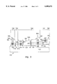
- FIG. 7 is a cross-sectional view of the integrated circuit after contact formation.
- the present invention is directed toward facilitating a method for fabricating an integrated circuit, such as a DRAM.
- the present invention will be shown to form a DRAM.
- the initial formation of the DRAM 150 is shown in FIG. 1.
- the DRAM is subsequently manufactured in accordance with the process steps in FIG. 2.
- the DRAM 150 is first fabricated by forming n and p wells in a base layer 103 (step 252), such as a silicon.
- active and field dielectric 102 areas are formed (step 254).
- gate dielectric 104 is formed on the base layer 103 (step 256).
- the gate dielectric 104 may be oxide or oxynitride.
- the oxide may be grown or deposited by conventional techniques.
- the field dielectric 102 may be an oxide, such as conventionally used field oxide.
- the conductor 107 may comprise one or more conductive layers, such as polysilicon 106 and tungsten silicide 108.
- the polysilicon 106 may be deposited and then doped, or deposited doped insitu.
- the tungsten silicide 108 may be formed by deposition or sputtering. Specific methods of forming the polysilicon 106 and tungsten silicide 108 are know to persons skilled in the art.
- an insulator 110 is deposited on the conductor 107 (step 260).
- the insulator 110 may be a nitride, an oxide or a combination thereof.
- the insulator 110 is silicon nitride.
- gate stacks are formed by patterning and removing material from the DRAM 150 (step 262), as shown in FIG. 3.
- the gate stacks may be wordlines 310 and gates 312. Removal is performed with a gate etch. Methods of patterning and removal to form gate stacks are known to persons skilled in the art.
- the active areas are doped by a conventional implant, otherwise known as a lightly doped drain (LDD) implant (step 264).
- LDD lightly doped drain
- n- and p-type dopants are implanted in self-alignment to the gate stacks into uncovered active regions of the corresponding n and p wells of the DRAM 150.
- the spacer 402 is formed on the sides of the wordlines 210 and gates 212 (step 266), as shown in FIG. 4.
- the spacer 402 can be comprised of one or more spacer insulators 411, 412.
- the spacer insulators 411, 412 may be oxides, nitrides or a combination thereof.
- the spacer 402 may be comprised of a first spacer insulator 411 that is an oxide grown on the sidewalls of the conductor.
- the second spacer insulator 412 an oxide or nitride, is formed on first spacer insulator 411, the insulator 110, the field oxide 104, and the base layer 103.
- only the second spacer insulator 412 may be formed on the DRAM 150.
- the second spacer insulator 412 may be a nitride film that is deposited and then etched back.
- an insulating film 520 is formed on the DRAM 150 (step 268), as shown in FIG. 5.
- the insulating film may be formed by depositing tetraethyloxysilicate (TEOS) 522 and borophosphosilicate glass (BPSG) 524 in succession on the DRAM 150.
- the TEOS 522 is undoped.
- the BPSG 524 is doped.
- the TEOS 522 and BPSG 524 have respective thicknesses of between 100 angstroms and 500 angstroms, and 1000 angstroms and 3000 angstroms. Deposition of the insulating film 520 is performed in a manner known to persons skilled in the art.
- the BPSG 524 is planarized (step 270) to about the height of the gate stacks with chemical mechanical planarization (CMP). Because BPSG 524 can be easily planarized and CMP is selective to nitride, a substantially flat topology is readily formed on the DRAM 150 surface. Conventionally, the TEOS 522 and BPSG 544 are used to form capacitors in the DRAM 150. However, the present invention also utilizes the insulating film 520 to provide the flat topology on the DRAM 150. The flat topology permits patterning the gate contact opening with lithography equipment having a reduced field of depth.
- CMP chemical mechanical planarization
- a gate contact opening 602 is formed by patterning and removing some insulating film 520, insulator 110, and spacer 402 (step 272), as shown in FIG. 6.
- the gate contact opening 602 exposes the conductor 107.
- the patterning of the gate contact opening 602 is defined with a mask.
- the removal is performed with a nitride etch, such as a dry etch, that removes the insulating film 520, insulator 110, and spacer 402 at about the same rate.
- additional insulating film 520 and some spacer 402 may also be removed. However, remaining insulating film 520 and the spacer 402 are sufficiently thick to prevent any field dielectric 102 from being removed. As a result, no undesirable short between the gate stack and the base layer 103 will occur. Thus, contact formation will not result in disabled transistors, and integrated circuit yield will increase.
- step 274 additional dielectric 760, is formed (step 274), by deposition for example, to create a capacitor container and an insulator between the contacts 750, 752 as shown in FIG. 7.
- the gate contact opening 602, again, and a bitline contact opening are defined, or formed, by patterning and removing some additional dielectric 760 (step 276).
- the patterning is accomplished with another mask.
- the removal is performed with an etch that will remove the additional dielectric 760, but substantially no spacer 402.
- an etch that is selective to nitride can be used to remove additional dielectric 760 which is not nitride, but no spacer 402 which is nitride.
- bitline and gate contacts 750, 752 can be formed (step 278) in self-alignment to the bitline and gate contact openings.
- the bitline and gate contacts 750, 752 can be formed by conventional metallization techniques.
Abstract
Description
Claims (16)
Priority Applications (2)
| Application Number | Priority Date | Filing Date | Title |
|---|---|---|---|
| US08/915,386 US6080672A (en) | 1997-08-20 | 1997-08-20 | Self-aligned contact formation for semiconductor devices |
| US09/515,804 US6207571B1 (en) | 1997-08-20 | 2000-02-29 | Self-aligned contact formation for semiconductor devices |
Applications Claiming Priority (1)
| Application Number | Priority Date | Filing Date | Title |
|---|---|---|---|
| US08/915,386 US6080672A (en) | 1997-08-20 | 1997-08-20 | Self-aligned contact formation for semiconductor devices |
Related Child Applications (1)
| Application Number | Title | Priority Date | Filing Date |
|---|---|---|---|
| US09/515,804 Continuation US6207571B1 (en) | 1997-08-20 | 2000-02-29 | Self-aligned contact formation for semiconductor devices |
Publications (1)
| Publication Number | Publication Date |
|---|---|
| US6080672A true US6080672A (en) | 2000-06-27 |
Family
ID=25435654
Family Applications (2)
| Application Number | Title | Priority Date | Filing Date |
|---|---|---|---|
| US08/915,386 Expired - Lifetime US6080672A (en) | 1997-08-20 | 1997-08-20 | Self-aligned contact formation for semiconductor devices |
| US09/515,804 Expired - Lifetime US6207571B1 (en) | 1997-08-20 | 2000-02-29 | Self-aligned contact formation for semiconductor devices |
Family Applications After (1)
| Application Number | Title | Priority Date | Filing Date |
|---|---|---|---|
| US09/515,804 Expired - Lifetime US6207571B1 (en) | 1997-08-20 | 2000-02-29 | Self-aligned contact formation for semiconductor devices |
Country Status (1)
| Country | Link |
|---|---|
| US (2) | US6080672A (en) |
Cited By (4)
| Publication number | Priority date | Publication date | Assignee | Title |
|---|---|---|---|---|
| US6417537B1 (en) | 2000-01-18 | 2002-07-09 | Micron Technology, Inc. | Metal oxynitride capacitor barrier layer |
| US6465828B2 (en) | 1999-07-30 | 2002-10-15 | Micron Technology, Inc. | Semiconductor container structure with diffusion barrier |
| US6576507B1 (en) * | 2000-11-14 | 2003-06-10 | International Business Machines Corporation | Selectively removable filler layer for BiCMOS process |
| US6649453B1 (en) | 2002-08-29 | 2003-11-18 | Micron Technology, Inc. | Contactless uniform-tunneling separate p-well (CUSP) non-volatile memory array architecture, fabrication and operation |
Families Citing this family (3)
| Publication number | Priority date | Publication date | Assignee | Title |
|---|---|---|---|---|
| US6627549B2 (en) | 2000-03-07 | 2003-09-30 | Micron Technology, Inc. | Methods for making nearly planar dielectric films in integrated circuits |
| DE10120929A1 (en) * | 2001-04-30 | 2002-10-31 | Infineon Technologies Ag | Manufacturing process for an integrated circuit |
| US6847092B2 (en) * | 2003-03-06 | 2005-01-25 | Infineon Technologies Ag | Microelectronic capacitor structure with radial current flow |
Citations (26)
| Publication number | Priority date | Publication date | Assignee | Title |
|---|---|---|---|---|
| US4354896A (en) * | 1980-08-05 | 1982-10-19 | Texas Instruments Incorporated | Formation of submicron substrate element |
| EP0111706A1 (en) * | 1982-12-07 | 1984-06-27 | International Business Machines Corporation | Sidewall isolation for gate of field effect transistor and process for the formation thereof |
| US4656732A (en) * | 1984-09-26 | 1987-04-14 | Texas Instruments Incorporated | Integrated circuit fabrication process |
| EP0265638A2 (en) * | 1986-10-28 | 1988-05-04 | International Business Machines Corporation | Lithographic image size reduction |
| US4792534A (en) * | 1985-12-25 | 1988-12-20 | Kabushiki Kaisha Toshiba | Method of manufacturing a semiconductor device involving sidewall spacer formation |
| US4801350A (en) * | 1986-12-29 | 1989-01-31 | Motorola, Inc. | Method for obtaining submicron features from optical lithography technology |
| US4912061A (en) * | 1988-04-04 | 1990-03-27 | Digital Equipment Corporation | Method of forming a salicided self-aligned metal oxide semiconductor device using a disposable silicon nitride spacer |
| US4962414A (en) * | 1988-02-11 | 1990-10-09 | Sgs-Thomson Microelectronics, Inc. | Method for forming a contact VIA |
| US5117273A (en) * | 1990-11-16 | 1992-05-26 | Sgs-Thomson Microelectronics, Inc. | Contact for integrated circuits |
| EP0491408A2 (en) * | 1990-11-20 | 1992-06-24 | Consorzio per la Ricerca sulla Microelettronica nel Mezzogiorno - CoRiMMe | Process for making planarized sub-micrometric trenches in integrated circuits |
| US5175127A (en) * | 1992-06-02 | 1992-12-29 | Micron Technology, Inc. | Self-aligned interlayer contact process using a plasma etch of photoresist |
| US5206187A (en) * | 1991-08-30 | 1993-04-27 | Micron Technology, Inc. | Method of processing semiconductor wafers using a contact etch stop |
| US5229326A (en) * | 1992-06-23 | 1993-07-20 | Micron Technology, Inc. | Method for making electrical contact with an active area through sub-micron contact openings and a semiconductor device |
| US5252517A (en) * | 1992-12-10 | 1993-10-12 | Micron Semiconductor, Inc. | Method of conductor isolation from a conductive contact plug |
| US5292677A (en) * | 1992-09-18 | 1994-03-08 | Micron Technology, Inc. | Reduced mask CMOS process for fabricating stacked capacitor multi-megabit dynamic random access memories utilizing single etch stop layer for contacts |
| US5300807A (en) * | 1992-01-22 | 1994-04-05 | The United States Of America As Represented By The Secretary Of The Army | Thin film detector and method of manufacture |
| US5362666A (en) * | 1992-09-18 | 1994-11-08 | Micron Technology, Inc. | Method of producing a self-aligned contact penetrating cell plate |
| US5411909A (en) * | 1993-02-22 | 1995-05-02 | Micron Technology, Inc. | Method of forming a planar thin film transistor |
| US5439846A (en) * | 1993-12-17 | 1995-08-08 | Sgs-Thomson Microelectronics, Inc. | Self-aligned method for forming contact with zero offset to gate |
| US5488011A (en) * | 1994-11-08 | 1996-01-30 | Micron Technology, Inc. | Method of forming contact areas between vertical conductors |
| US5498570A (en) * | 1994-09-15 | 1996-03-12 | Micron Technology Inc. | Method of reducing overetch during the formation of a semiconductor device |
| US5605864A (en) * | 1994-08-02 | 1997-02-25 | Micron Technology, Inc. | Method for forming a semiconductor buried contact with a removable spacer |
| US5688720A (en) * | 1992-04-15 | 1997-11-18 | Nec Corporation | Method of flattening the surface of a semiconductor device by polishing |
| US5724282A (en) * | 1996-09-06 | 1998-03-03 | Micron Technology, Inc. | System and method for an antifuse bank |
| US5863837A (en) * | 1996-03-22 | 1999-01-26 | Kabushiki Kaisha Toshiba | Method of manufacturing semiconductor device |
| US5914279A (en) * | 1996-04-26 | 1999-06-22 | Texas Instruments Incorporated | Silicon nitride sidewall and top surface layer separating conductors |
-
1997
- 1997-08-20 US US08/915,386 patent/US6080672A/en not_active Expired - Lifetime
-
2000
- 2000-02-29 US US09/515,804 patent/US6207571B1/en not_active Expired - Lifetime
Patent Citations (27)
| Publication number | Priority date | Publication date | Assignee | Title |
|---|---|---|---|---|
| US4354896A (en) * | 1980-08-05 | 1982-10-19 | Texas Instruments Incorporated | Formation of submicron substrate element |
| EP0111706A1 (en) * | 1982-12-07 | 1984-06-27 | International Business Machines Corporation | Sidewall isolation for gate of field effect transistor and process for the formation thereof |
| US4656732A (en) * | 1984-09-26 | 1987-04-14 | Texas Instruments Incorporated | Integrated circuit fabrication process |
| US4792534A (en) * | 1985-12-25 | 1988-12-20 | Kabushiki Kaisha Toshiba | Method of manufacturing a semiconductor device involving sidewall spacer formation |
| EP0265638A2 (en) * | 1986-10-28 | 1988-05-04 | International Business Machines Corporation | Lithographic image size reduction |
| US4801350A (en) * | 1986-12-29 | 1989-01-31 | Motorola, Inc. | Method for obtaining submicron features from optical lithography technology |
| US4962414A (en) * | 1988-02-11 | 1990-10-09 | Sgs-Thomson Microelectronics, Inc. | Method for forming a contact VIA |
| US4912061A (en) * | 1988-04-04 | 1990-03-27 | Digital Equipment Corporation | Method of forming a salicided self-aligned metal oxide semiconductor device using a disposable silicon nitride spacer |
| US5117273A (en) * | 1990-11-16 | 1992-05-26 | Sgs-Thomson Microelectronics, Inc. | Contact for integrated circuits |
| EP0491408A2 (en) * | 1990-11-20 | 1992-06-24 | Consorzio per la Ricerca sulla Microelettronica nel Mezzogiorno - CoRiMMe | Process for making planarized sub-micrometric trenches in integrated circuits |
| US5206187A (en) * | 1991-08-30 | 1993-04-27 | Micron Technology, Inc. | Method of processing semiconductor wafers using a contact etch stop |
| US5300807A (en) * | 1992-01-22 | 1994-04-05 | The United States Of America As Represented By The Secretary Of The Army | Thin film detector and method of manufacture |
| US5688720A (en) * | 1992-04-15 | 1997-11-18 | Nec Corporation | Method of flattening the surface of a semiconductor device by polishing |
| US5175127A (en) * | 1992-06-02 | 1992-12-29 | Micron Technology, Inc. | Self-aligned interlayer contact process using a plasma etch of photoresist |
| US5229326A (en) * | 1992-06-23 | 1993-07-20 | Micron Technology, Inc. | Method for making electrical contact with an active area through sub-micron contact openings and a semiconductor device |
| US5292677A (en) * | 1992-09-18 | 1994-03-08 | Micron Technology, Inc. | Reduced mask CMOS process for fabricating stacked capacitor multi-megabit dynamic random access memories utilizing single etch stop layer for contacts |
| US5362666A (en) * | 1992-09-18 | 1994-11-08 | Micron Technology, Inc. | Method of producing a self-aligned contact penetrating cell plate |
| US5252517A (en) * | 1992-12-10 | 1993-10-12 | Micron Semiconductor, Inc. | Method of conductor isolation from a conductive contact plug |
| US5411909A (en) * | 1993-02-22 | 1995-05-02 | Micron Technology, Inc. | Method of forming a planar thin film transistor |
| US5439846A (en) * | 1993-12-17 | 1995-08-08 | Sgs-Thomson Microelectronics, Inc. | Self-aligned method for forming contact with zero offset to gate |
| US5605864A (en) * | 1994-08-02 | 1997-02-25 | Micron Technology, Inc. | Method for forming a semiconductor buried contact with a removable spacer |
| US5498570A (en) * | 1994-09-15 | 1996-03-12 | Micron Technology Inc. | Method of reducing overetch during the formation of a semiconductor device |
| US5488011A (en) * | 1994-11-08 | 1996-01-30 | Micron Technology, Inc. | Method of forming contact areas between vertical conductors |
| US5863837A (en) * | 1996-03-22 | 1999-01-26 | Kabushiki Kaisha Toshiba | Method of manufacturing semiconductor device |
| US5914279A (en) * | 1996-04-26 | 1999-06-22 | Texas Instruments Incorporated | Silicon nitride sidewall and top surface layer separating conductors |
| US5724282A (en) * | 1996-09-06 | 1998-03-03 | Micron Technology, Inc. | System and method for an antifuse bank |
| US5872740A (en) * | 1996-09-06 | 1999-02-16 | Micron Technology, Inc. | System and method for an antifuse bank |
Non-Patent Citations (10)
| Title |
|---|
| "Method to Produce Sizesin Openings in Photo Images Smaller than Lithographic Minimum Size", IBM Technical Disclosure Bulletin, 29, 1328, (Aug. 1986). |
| "Methods of Forming Small Contact Holes", IBM Technical Disclosure Bulletin, 30, 252, (Jan. 1988). |
| Fukase, T., et al., "A Margin-Free Contact Process Using An Al2 O3 Etch-Stop Layer for High Density Devices", International Electron Devices Meeting: Technical Digest, 837-840, (1992). |
| Fukase, T., et al., A Margin Free Contact Process Using An Al 2 O 3 Etch Stop Layer for High Density Devices , International Electron Devices Meeting: Technical Digest , 837 840, (1992). * |
| Lau, C., et al., "A Super Self-Aligned Source/Drain MOSFET", International Electron Devices Meeting: Technical Digest, 358-361, (1987). |
| Lau, C., et al., A Super Self Aligned Source/Drain MOSFET , International Electron Devices Meeting: Technical Digest , 358 361, (1987). * |
| Method to Produce Sizesin Openings in Photo Images Smaller than Lithographic Minimum Size , IBM Technical Disclosure Bulletin , 29, 1328, (Aug. 1986). * |
| Methods of Forming Small Contact Holes , IBM Technical Disclosure Bulletin , 30, 252, (Jan. 1988). * |
| Singer, P., "A New Technology for Oxide Contact and Via Etch", Semiconductor International, 36, (Aug. 1993). |
| Singer, P., A New Technology for Oxide Contact and Via Etch , Semiconductor International , 36, (Aug. 1993). * |
Cited By (19)
| Publication number | Priority date | Publication date | Assignee | Title |
|---|---|---|---|---|
| US6465828B2 (en) | 1999-07-30 | 2002-10-15 | Micron Technology, Inc. | Semiconductor container structure with diffusion barrier |
| US6780706B2 (en) | 1999-07-30 | 2004-08-24 | Micron Technology, Inc. | Semiconductor container structure with diffusion barrier |
| US7002202B2 (en) | 2000-01-18 | 2006-02-21 | Micron Technology, Inc. | Metal oxynitride capacitor barrier layer |
| US6631069B2 (en) | 2000-01-18 | 2003-10-07 | Micron Technology, Inc. | Metal oxynitride capacitor barrier layer |
| US7015527B2 (en) | 2000-01-18 | 2006-03-21 | Micron Technology, Inc. | Metal oxynitride capacitor barrier layer |
| US6664583B2 (en) | 2000-01-18 | 2003-12-16 | Micron Technology, Inc. | Metal oxynitride capacitor barrier layer |
| US6664584B2 (en) | 2000-01-18 | 2003-12-16 | Micron Technology, Inc. | Metal oxynitride capacitor barrier layer |
| US6670256B2 (en) | 2000-01-18 | 2003-12-30 | Micron Technology, Inc. | Metal oxynitride capacitor barrier layer |
| US6417537B1 (en) | 2000-01-18 | 2002-07-09 | Micron Technology, Inc. | Metal oxynitride capacitor barrier layer |
| US20040085802A1 (en) * | 2000-01-18 | 2004-05-06 | Micron Technology, Inc. | Metal oxynitride capacitor barrier layer |
| US6576507B1 (en) * | 2000-11-14 | 2003-06-10 | International Business Machines Corporation | Selectively removable filler layer for BiCMOS process |
| US20040071008A1 (en) * | 2002-08-29 | 2004-04-15 | Micron Technology, Inc. | Contactless uniform-tunneling separate p-well (CUSP) non-volatile memory array architecture, fabrication and operation |
| US6930350B2 (en) | 2002-08-29 | 2005-08-16 | Micron Technology, Inc. | Contactless uniform-tunneling separate p-well (CUSP) non-volatile memory array architecture, fabrication and operation |
| US6984547B2 (en) | 2002-08-29 | 2006-01-10 | Micron Technology, Inc. | Contactless uniform-tunneling separate p-well (cusp) non-volatile memory array architecture, fabrication and operation |
| US20050099846A1 (en) * | 2002-08-29 | 2005-05-12 | Micron Technology, Inc. | Contactless uniform-tunneling separate P-well (CUSP) non-volatile memory array architecture, fabrication and operation |
| US6649453B1 (en) | 2002-08-29 | 2003-11-18 | Micron Technology, Inc. | Contactless uniform-tunneling separate p-well (CUSP) non-volatile memory array architecture, fabrication and operation |
| US7199422B2 (en) | 2002-08-29 | 2007-04-03 | Micron Technology, Inc. | Contactless uniform-tunneling separate P-well (CUSP) non-volatile memory array architecture, fabrication and operation |
| US20070164348A1 (en) * | 2002-08-29 | 2007-07-19 | Micron Technology, Inc. | Contactless uniform-tunneling separate p-well (cusp)non-volatile memory array architecture, fabrication and operation |
| US7696557B2 (en) | 2002-08-29 | 2010-04-13 | Micron Technology, Inc. | Contactless uniform-tunneling separate p-well (CUSP) non-volatile memory array architecture, fabrication and operation |
Also Published As
| Publication number | Publication date |
|---|---|
| US6207571B1 (en) | 2001-03-27 |
Similar Documents
| Publication | Publication Date | Title |
|---|---|---|
| US5150276A (en) | Method of fabricating a vertical parallel cell capacitor having a storage node capacitor plate comprising a center fin effecting electrical communication between itself and parallel annular rings | |
| US5780339A (en) | Method for fabricating a semiconductor memory cell in a DRAM | |
| US6096595A (en) | Integration of a salicide process for MOS logic devices, and a self-aligned contact process for MOS memory devices | |
| US5663092A (en) | Methods of fabricating a transistor cell with a high aspect ratio buried contact | |
| KR100322218B1 (en) | Semiconductor device and method of manufacturing the same | |
| US5258096A (en) | Method of forming local etch stop landing pads for simultaneous, self-aligned dry etching of contact vias with various depths | |
| US6037261A (en) | Semiconductor processing method of making electrical contact to a node received within a mass of insulating dielectric material | |
| EP1122772A2 (en) | Method of forming self-aligned contact structures in semiconductor integrated circuit devices | |
| US20060202340A1 (en) | Semiconductor device and method of manufacturing the same | |
| US6080620A (en) | Method for fabricating interconnection and capacitors of a DRAM using a simple geometry active area, self-aligned etching, and polysilicon plugs | |
| US6165839A (en) | Process to fabricate a cylindrical, capacitor structure under a bit line structure for a dynamic random access memory cell | |
| US6037211A (en) | Method of fabricating contact holes in high density integrated circuits using polysilicon landing plug and self-aligned etching processes | |
| EP0996151B1 (en) | Method for fabricating transistors | |
| US6333233B1 (en) | Semiconductor device with self-aligned contact and its manufacture | |
| US6184079B1 (en) | Method for fabricating a semiconductor device | |
| US6080672A (en) | Self-aligned contact formation for semiconductor devices | |
| US6423620B2 (en) | Semiconductor processing methods of forming contact openings, methods of forming memory circuitry, methods of forming electrical connections, and methods of forming dynamic random access memory dram circuitry | |
| KR100310565B1 (en) | A semiconductor device and a method for fabricating the same | |
| US5723374A (en) | Method for forming dielectric spacer to prevent poly stringer in stacked capacitor DRAM technology | |
| US6383921B1 (en) | Self aligned silicide contact method of fabrication | |
| US6404020B1 (en) | Method of forming contact pads in a semiconductor device and a semiconductor device formed using the method | |
| KR100273706B1 (en) | Method for manufacturing semiconductor device | |
| KR100348315B1 (en) | Method for Fabricating of Semiconductor Device | |
| KR100333360B1 (en) | A method of fabricating a semiconductor device | |
| KR20000009277A (en) | Method for forming contact hole in semiconductor memory device |
Legal Events
| Date | Code | Title | Description |
|---|---|---|---|
| AS | Assignment |
Owner name: MICRON TECHNOLOGY, INC., IDAHO Free format text: ASSIGNMENT OF ASSIGNORS INTEREST;ASSIGNORS:JUENGLING, WERNER;PRALL, KIRK D.;DOAN, TRUNG T.;AND OTHERS;REEL/FRAME:009320/0917;SIGNING DATES FROM 19971003 TO 19971020 |
|
| STCF | Information on status: patent grant |
Free format text: PATENTED CASE |
|
| FEPP | Fee payment procedure |
Free format text: PAYOR NUMBER ASSIGNED (ORIGINAL EVENT CODE: ASPN); ENTITY STATUS OF PATENT OWNER: LARGE ENTITY |
|
| FPAY | Fee payment |
Year of fee payment: 4 |
|
| FPAY | Fee payment |
Year of fee payment: 8 |
|
| FPAY | Fee payment |
Year of fee payment: 12 |
|
| AS | Assignment |
Owner name: U.S. BANK NATIONAL ASSOCIATION, AS COLLATERAL AGENT, CALIFORNIA Free format text: SECURITY INTEREST;ASSIGNOR:MICRON TECHNOLOGY, INC.;REEL/FRAME:038669/0001 Effective date: 20160426 Owner name: U.S. BANK NATIONAL ASSOCIATION, AS COLLATERAL AGEN Free format text: SECURITY INTEREST;ASSIGNOR:MICRON TECHNOLOGY, INC.;REEL/FRAME:038669/0001 Effective date: 20160426 |
|
| AS | Assignment |
Owner name: MORGAN STANLEY SENIOR FUNDING, INC., AS COLLATERAL AGENT, MARYLAND Free format text: PATENT SECURITY AGREEMENT;ASSIGNOR:MICRON TECHNOLOGY, INC.;REEL/FRAME:038954/0001 Effective date: 20160426 Owner name: MORGAN STANLEY SENIOR FUNDING, INC., AS COLLATERAL Free format text: PATENT SECURITY AGREEMENT;ASSIGNOR:MICRON TECHNOLOGY, INC.;REEL/FRAME:038954/0001 Effective date: 20160426 |
|
| AS | Assignment |
Owner name: U.S. BANK NATIONAL ASSOCIATION, AS COLLATERAL AGENT, CALIFORNIA Free format text: CORRECTIVE ASSIGNMENT TO CORRECT THE REPLACE ERRONEOUSLY FILED PATENT #7358718 WITH THE CORRECT PATENT #7358178 PREVIOUSLY RECORDED ON REEL 038669 FRAME 0001. ASSIGNOR(S) HEREBY CONFIRMS THE SECURITY INTEREST;ASSIGNOR:MICRON TECHNOLOGY, INC.;REEL/FRAME:043079/0001 Effective date: 20160426 Owner name: U.S. BANK NATIONAL ASSOCIATION, AS COLLATERAL AGEN Free format text: CORRECTIVE ASSIGNMENT TO CORRECT THE REPLACE ERRONEOUSLY FILED PATENT #7358718 WITH THE CORRECT PATENT #7358178 PREVIOUSLY RECORDED ON REEL 038669 FRAME 0001. ASSIGNOR(S) HEREBY CONFIRMS THE SECURITY INTEREST;ASSIGNOR:MICRON TECHNOLOGY, INC.;REEL/FRAME:043079/0001 Effective date: 20160426 |
|
| AS | Assignment |
Owner name: MICRON TECHNOLOGY, INC., IDAHO Free format text: RELEASE BY SECURED PARTY;ASSIGNOR:U.S. BANK NATIONAL ASSOCIATION, AS COLLATERAL AGENT;REEL/FRAME:047243/0001 Effective date: 20180629 |
|
| AS | Assignment |
Owner name: MICRON TECHNOLOGY, INC., IDAHO Free format text: RELEASE BY SECURED PARTY;ASSIGNOR:MORGAN STANLEY SENIOR FUNDING, INC., AS COLLATERAL AGENT;REEL/FRAME:050937/0001 Effective date: 20190731 |