US6084258A - Metal-semiconductor junction fet - Google Patents
Metal-semiconductor junction fet Download PDFInfo
- Publication number
- US6084258A US6084258A US08/876,987 US87698797A US6084258A US 6084258 A US6084258 A US 6084258A US 87698797 A US87698797 A US 87698797A US 6084258 A US6084258 A US 6084258A
- Authority
- US
- United States
- Prior art keywords
- layer
- mesfet
- substrate body
- source
- semiconductor substrate
- Prior art date
- Legal status (The legal status is an assumption and is not a legal conclusion. Google has not performed a legal analysis and makes no representation as to the accuracy of the status listed.)
- Expired - Fee Related
Links
- 239000004065 semiconductor Substances 0.000 title claims abstract description 23
- 239000000758 substrate Substances 0.000 claims abstract description 39
- 229910001218 Gallium arsenide Inorganic materials 0.000 claims abstract description 28
- 229910052737 gold Inorganic materials 0.000 claims abstract 2
- 229910052697 platinum Inorganic materials 0.000 claims abstract 2
- 229910052719 titanium Inorganic materials 0.000 claims abstract 2
- 229910045601 alloy Inorganic materials 0.000 claims description 6
- 239000000956 alloy Substances 0.000 claims description 6
- 238000000151 deposition Methods 0.000 claims description 5
- 239000012212 insulator Substances 0.000 claims description 5
- 230000005669 field effect Effects 0.000 claims description 3
- 229910052759 nickel Inorganic materials 0.000 claims description 3
- 230000015572 biosynthetic process Effects 0.000 claims 2
- 229910052710 silicon Inorganic materials 0.000 claims 2
- 239000010703 silicon Substances 0.000 claims 2
- 238000004519 manufacturing process Methods 0.000 abstract description 10
- 229910000530 Gallium indium arsenide Inorganic materials 0.000 abstract description 5
- VYPSYNLAJGMNEJ-UHFFFAOYSA-N Silicium dioxide Chemical compound O=[Si]=O VYPSYNLAJGMNEJ-UHFFFAOYSA-N 0.000 description 20
- 229920002120 photoresistant polymer Polymers 0.000 description 16
- 229910052681 coesite Inorganic materials 0.000 description 10
- 229910052906 cristobalite Inorganic materials 0.000 description 10
- 239000000377 silicon dioxide Substances 0.000 description 10
- 229910052682 stishovite Inorganic materials 0.000 description 10
- 229910052905 tridymite Inorganic materials 0.000 description 10
- 238000000034 method Methods 0.000 description 8
- NBIIXXVUZAFLBC-UHFFFAOYSA-N Phosphoric acid Chemical compound OP(O)(O)=O NBIIXXVUZAFLBC-UHFFFAOYSA-N 0.000 description 4
- 230000008569 process Effects 0.000 description 4
- 230000008021 deposition Effects 0.000 description 3
- 238000000059 patterning Methods 0.000 description 3
- 229910000147 aluminium phosphate Inorganic materials 0.000 description 2
- 230000008018 melting Effects 0.000 description 2
- 238000002844 melting Methods 0.000 description 2
- 239000000203 mixture Substances 0.000 description 2
- 230000004048 modification Effects 0.000 description 2
- 238000012986 modification Methods 0.000 description 2
- 229960004838 phosphoric acid Drugs 0.000 description 2
- 235000011007 phosphoric acid Nutrition 0.000 description 2
- 238000001020 plasma etching Methods 0.000 description 2
- 238000001039 wet etching Methods 0.000 description 2
- 241000237518 Arion Species 0.000 description 1
- 230000004075 alteration Effects 0.000 description 1
- 150000001875 compounds Chemical class 0.000 description 1
- 238000010438 heat treatment Methods 0.000 description 1
- 239000007769 metal material Substances 0.000 description 1
- 238000003801 milling Methods 0.000 description 1
- 238000004544 sputter deposition Methods 0.000 description 1
- 238000000992 sputter etching Methods 0.000 description 1
Images


Classifications
-
- H—ELECTRICITY
- H01—ELECTRIC ELEMENTS
- H01L—SEMICONDUCTOR DEVICES NOT COVERED BY CLASS H10
- H01L29/00—Semiconductor devices adapted for rectifying, amplifying, oscillating or switching, or capacitors or resistors with at least one potential-jump barrier or surface barrier, e.g. PN junction depletion layer or carrier concentration layer; Details of semiconductor bodies or of electrodes thereof ; Multistep manufacturing processes therefor
- H01L29/66—Types of semiconductor device ; Multistep manufacturing processes therefor
- H01L29/66007—Multistep manufacturing processes
- H01L29/66075—Multistep manufacturing processes of devices having semiconductor bodies comprising group 14 or group 13/15 materials
- H01L29/66227—Multistep manufacturing processes of devices having semiconductor bodies comprising group 14 or group 13/15 materials the devices being controllable only by the electric current supplied or the electric potential applied, to an electrode which does not carry the current to be rectified, amplified or switched, e.g. three-terminal devices
- H01L29/66409—Unipolar field-effect transistors
- H01L29/66848—Unipolar field-effect transistors with a Schottky gate, i.e. MESFET
- H01L29/66856—Unipolar field-effect transistors with a Schottky gate, i.e. MESFET with an active layer made of a group 13/15 material
- H01L29/66863—Lateral single gate transistors
-
- H—ELECTRICITY
- H01—ELECTRIC ELEMENTS
- H01L—SEMICONDUCTOR DEVICES NOT COVERED BY CLASS H10
- H01L29/00—Semiconductor devices adapted for rectifying, amplifying, oscillating or switching, or capacitors or resistors with at least one potential-jump barrier or surface barrier, e.g. PN junction depletion layer or carrier concentration layer; Details of semiconductor bodies or of electrodes thereof ; Multistep manufacturing processes therefor
- H01L29/66—Types of semiconductor device ; Multistep manufacturing processes therefor
- H01L29/68—Types of semiconductor device ; Multistep manufacturing processes therefor controllable by only the electric current supplied, or only the electric potential applied, to an electrode which does not carry the current to be rectified, amplified or switched
- H01L29/76—Unipolar devices, e.g. field effect transistors
- H01L29/772—Field effect transistors
- H01L29/80—Field effect transistors with field effect produced by a PN or other rectifying junction gate, i.e. potential-jump barrier
- H01L29/812—Field effect transistors with field effect produced by a PN or other rectifying junction gate, i.e. potential-jump barrier with a Schottky gate
Definitions
- the present invention relates to a metal-semiconductor junction field effect transistor (MESFET) and, more particularly, to a structure of electrodes of a MESFET.
- MESFET metal-semiconductor junction field effect transistor
- FIGS. 1A to 1K Various methods have been used in fabrication of a MESFET to form electrodes and interconnects thereof. A method for manufacturing a conventional GaAs MESFET will be described first with reference to FIGS. 1A to 1K.
- a GaAs substrate designated by reference numeral 100 includes a substrate body 101 made of undoped GaAs (i-GaAs) and an n + -GaAs layer 102 doped with Si at a concentration of 2 ⁇ 10 18 atoms/cm 3 and formed on the substrate body 101 to a thickness of 60 nanometers (nm).
- i-GaAs undoped GaAs
- n + -GaAs layer 102 doped with Si at a concentration of 2 ⁇ 10 18 atoms/cm 3 and formed on the substrate body 101 to a thickness of 60 nanometers (nm).
- a SiO 2 film 2 is formed on the GaAs substrate 100 to a thickness of 300 nm (FIG. 1A).
- a photoresist pattern 26 is then formed on the SiO 2 film 2, and a gate electrode opening 27 is formed in the SiO 2 film 2 by reactive ion etching with CF 4 gas and using the photoresist pattern 26 as a mask (FIG. 1B).
- a surface portion of the n + -GaAs layer 102 of the GaAs substrate 100 exposed in the gate electrode opening 27 is removed by a wet etching using a phosphoric-acid-based etchant, whereby a gate recess 28 is formed on the n + -GaAs layer 102 beneath the gate electrode opening 27 (FIG. 1C).
- the recess 28 is formed in order to adjust the threshold voltage of the finished MESFET.
- a WSi x metallic film 29 having a high melting point and a relatively high resistivity is deposited by sputtering in a thickness of 500 nm (FIG. 1D), and subjected to patterning together with the SiO 2 film 2 to form a gate electrode 29A by reactive ion ethching with CF 4 and SF 6 gas mixture and using a second photoresist film 31 as a mask, gate electrode 29A having a Schottky contact 30 between the same and the n + -GaAs layer 102 (FIG. 1E).
- a third photoresist pattern 42 is formed to cover the gate electrode 29A, the photoresist pattern 31 having openings 43 for exposing the n + -GaAs layer 102 at the locations where source and drain electrodes are to be formed.
- a metallic laminate 44 including AuGe/Ni/Au films is then deposited on the entire surface including the surface of the n + -GaAs layer 102 at the bottom of the openings 43 (FIG. 1F).
- the metallic laminate 44 formed on the photoresist pattern 42 is then removed by a lift-off method.
- a heat treatment is then performed to form alloy ohmic contacts 44A between the source and drain electrodes to be formed and the n + -GaAs layer 102 (FIG. 1G).
- a second SiO 2 film 32 is deposited (FIG. 1H) on the entire surface and subjected to planarization (FIG. 1I).
- a gate electrode contact hole 34, a source electrode contact hole 35, and a drain electrode contact hole 36 are formed in the SiO 2 film 32 by a photolithographic technique using a fourth photoresist pattern 33 as a mask (FIG. 1J).
- a metallic laminate 37 including Ti/Pt/Au films and having a small resistance is deposited on the entire surface including the surfaces of SiO 2 film 32, gate electrode 29A and the alloy ohmic contacts 44A for the source and drain (FIG. 1K).
- the metallic laminate 37 is then subjected to patterning by Arion milling and using a fifth photoresist pattern 38 as a mask, thereby obtaining source electrode 40, gate interconnect 39 and drain electrode 41 (FIG. 1L).
- a finished MESFET is obtained (FIG. 1K).
- the Ti/Pt/Au metallic laminate 39, 40, 41 has a small resistance to thereby obtain a high speed operation of the resultant MESFET.
- the present invention is directed to a MESFET comprising: a substrate including a semiconductor substrate body and a first layer formed on said substrate body, said first layer having a hole exposing a portion of said substrate body; an insulator layer formed on said first layer and having first, second and third openings consecutively arranged, said second openings being disposed above said hole; a metallic laminate implementing gate, source and drain electrodes formed on said insulator layer, said source and drain electrodes passing said first and third openings, respectively, to contact said first layer in ohmic contacts, said gate electrode passing said second opening and said hole to contact said substrate body in a Schottky contact.
- a single metallic laminate can be patterned to obtain gate, source and drain electrodes, so that the number of deposition and photolithographic steps can be reduced, thereby reducing the fabrication cost of the MESFET.
- FIGS. 1A to 1M are cross-sectional views of a conventional MESFET in consecutive steps of a process for manufacturing the MESFET;
- FIGS. 2A to 2F are cross-sectional views of a MESFET according to an embodiment of the present in consecutive steps of a process for manufacturing the MESFET;
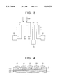
- FIG. 3 is a plan view showing a practical layout of interconnects of MESFETs according to the embodiment of FIGS. 2A to 2F;
- FIG. 4 is a cross-sectional view taken along line I--I in FIG. 3.
- FIGS. 2A to 2F show a process for manufacturing a MESFET according to the embodiment of the present invention.
- a compound semiconductor substrate 1 has a substrate body or base 101 made of undoped GaAs (i-GaAs), an n + -GaAs layer 102 doped with Si at a concentration of 2 ⁇ 10 18 atoms/cm 3 and grown on the substrate body 101 to a thickness of 60 nm, and an n + -In 0 .3 Ga 0 .7 As layer 103 doped with Si at a concentration of 1 ⁇ 10 19 atoms/cm 3 and grown on the n + -GaAs layer 102 to a thickness of 30 nm.
- a SiO 2 film 2 is formed to a thickness of 300 nm.
- a gate electrode opening 4, a source electrode opening 5, and a drain electrode opening 6 consecutively arranged in a row are formed in the SiO 2 film 2 (FIG. 2B).
- the source electrode opening 5 and the drain electrode opening 6 are covered with a second photoresist pattern 7.
- n + -In 0 .3 Ga 0 .7 As layer 103 of the substrate 1 exposed in the gate electrode opening 4 is removed by a wet etching using a phosphoric-acid-based etchant, so that a hole 8 is formed in the n + -In 0 .3 Ga 0 .7 As layer 103 for exposing n + -GaAs layer 102 of the substrate 1 (FIG. 2C).
- a WSi x /Ti/Pt/Au metallic laminate 9 including consecutively, as viewed from the bottom, a 50 nm-thick WSi x film, a 10 nm-thick Ti film, a 30 nm-thick Pt film and a 410 nm-thick Au film is formed (FIG. 2D).
- the metallic laminate 9 is selectively etched by Ar-ion milling and using a second photoresist pattern 13 as a mask (FIG.
- WSi x /Ti/Pt/Au laminate including WSi x film having a high melting point and Ti/Pt/Au films having a small resistance, allows the gate, source and drain electrodes and corresponding interconnects to be formed from a single combination of metallic materials.
- the substrate may be formed of a n + -GaAS substrate body and a single n + -InGaAs layer instead of the two layer structure formed on the undoped substrate body.
- the n + -InGaAs layer may have a composition In x Ga 1-x As wherein x is between 0.1 and 0.9.
- the concentration of Si in the n-GaAs layer 102 may be in the range between about 1 ⁇ 10 17 and about 5 ⁇ 10 18 atoms/cm 3 while the concentration of Si in the n + -InGaAs layer 103 may be in the range between about 1 ⁇ 10 19 and about 1 ⁇ 10 20 atoms/cm 3 .
- a n + -GaAs substrate doped with Si at a concentration of 2 ⁇ 10 18 may be used in which the second layer of the substrate is substantially made of an alloy film including Ni and Ge, for example, where part of the Ge is diffused into the n + -GaAs layer to form an ohmic contact between the Ni/Ge layer and the n + -GaAs layer, and having a hole for the gate electrode contacting the first layer in a Schottky contact.
- FIGS. 3 and 4 show an exemplified practical layout of electrodes of MESFETs according to the embodiment as described above.
- FIG. 3 is a schematic plan view of the electrodes and interconnects of the MESFETs while FIG. 4 is a sectional view taken along line A--A in FIG. 3.
- FIGS. 3 and 4 includes two MESFETs including a driver FET and a load FET therefor.
- the electrodes and interconnects of the MESFETs are formed from a single WSi x /Ti/Pt/Au laminate by a single step of patterning such as executed at the step shown in FIG. 2E.
- the drain electrode 17 and the source electrode 19 of the load FET are opposed to each other, with the gate electrode 18 of the load FET being interposed therebetween, while the drain electrode 19 and source electrode 21 of the driver FET are opposed to each other, with the gate electrode 20 of the drive FET being interposed therebetween.
- the source electrode 19 of the load FET and the drain electrode 19 of the driver FET are implemented by the same electrode.
- the electrode 19 serves as both the source electrode of the load FET and the drain electrode of the driver FET.
- the gate electrode 18 and the source electrode 19 of the load FET are connected together to a pad 25.
- the drain electrode of the load FET, the gate electrode and the source electrode of the driver FET are connected to pad 22, pad 23 and 24 respectively.
- the electrodes 17 through 21 are consecutively arranged in a row to form two of the MESFETs provided by the embodiment as described before.
- the gate electrodes 18 and 20 contact the n + -GaAs layer 102 in a Schottky contact while the source and drain electrodes 17, 19 and 21 contact the n + -InGaAs layer 103 in an ohmic contact.
Abstract
A MESFET has a metallic laminate including WSix, Ti, Pt and Au films and implementing gate, source and drain electrodes of the MESFET and interconnects therefor. The substrate of the MESFET is formed of a substrate body, a first semiconductor layer made of n+ -GaAs doped with Si at a concentration of 2×10¹⁸ atoms/cm3 and a second semiconductor layer made of n+ -InGaAs doped with Si at a concentration of 1×10¹⁹ atoms/cm3. The source and drain electrodes contact the second semiconductor layer in an ohmic contact while the gate electrode contacts the first semiconductor layer in a Schottky contact through a hole formed in the second semiconductor layer. A reduced number of steps in manufacture of the MESFET can be obtained, thereby reducing fabrication costs of the MESFET.
Description
This is a continuation of application Ser. No. 08/602,466 filed on Feb. 16, 1996, now abandoned.
(a) Field of the Invention
The present invention relates to a metal-semiconductor junction field effect transistor (MESFET) and, more particularly, to a structure of electrodes of a MESFET.
(b) Description of the Related Art
Various methods have been used in fabrication of a MESFET to form electrodes and interconnects thereof. A method for manufacturing a conventional GaAs MESFET will be described first with reference to FIGS. 1A to 1K.
A GaAs substrate designated by reference numeral 100 includes a substrate body 101 made of undoped GaAs (i-GaAs) and an n+ -GaAs layer 102 doped with Si at a concentration of 2×10¹⁸ atoms/cm3 and formed on the substrate body 101 to a thickness of 60 nanometers (nm).
First, a SiO2 film 2 is formed on the GaAs substrate 100 to a thickness of 300 nm (FIG. 1A). A photoresist pattern 26 is then formed on the SiO2 film 2, and a gate electrode opening 27 is formed in the SiO2 film 2 by reactive ion etching with CF4 gas and using the photoresist pattern 26 as a mask (FIG. 1B). After removal of the photoresist pattern 26, a surface portion of the n+ -GaAs layer 102 of the GaAs substrate 100 exposed in the gate electrode opening 27 is removed by a wet etching using a phosphoric-acid-based etchant, whereby a gate recess 28 is formed on the n+ -GaAs layer 102 beneath the gate electrode opening 27 (FIG. 1C). The recess 28 is formed in order to adjust the threshold voltage of the finished MESFET.
Subsequently, a WSix metallic film 29 having a high melting point and a relatively high resistivity is deposited by sputtering in a thickness of 500 nm (FIG. 1D), and subjected to patterning together with the SiO2 film 2 to form a gate electrode 29A by reactive ion ethching with CF4 and SF6 gas mixture and using a second photoresist film 31 as a mask, gate electrode 29A having a Schottky contact 30 between the same and the n+ -GaAs layer 102 (FIG. 1E). After removal of the second photoresist pattern 31, a third photoresist pattern 42 is formed to cover the gate electrode 29A, the photoresist pattern 31 having openings 43 for exposing the n+ -GaAs layer 102 at the locations where source and drain electrodes are to be formed. A metallic laminate 44 including AuGe/Ni/Au films is then deposited on the entire surface including the surface of the n+ -GaAs layer 102 at the bottom of the openings 43 (FIG. 1F). The metallic laminate 44 formed on the photoresist pattern 42 is then removed by a lift-off method. A heat treatment is then performed to form alloy ohmic contacts 44A between the source and drain electrodes to be formed and the n+ -GaAs layer 102 (FIG. 1G).
Thereafter, a second SiO2 film 32 is deposited (FIG. 1H) on the entire surface and subjected to planarization (FIG. 1I). Subsequently, a gate electrode contact hole 34, a source electrode contact hole 35, and a drain electrode contact hole 36 are formed in the SiO2 film 32 by a photolithographic technique using a fourth photoresist pattern 33 as a mask (FIG. 1J).
After removal of the photoresist pattern 33, a metallic laminate 37 including Ti/Pt/Au films and having a small resistance is deposited on the entire surface including the surfaces of SiO2 film 32, gate electrode 29A and the alloy ohmic contacts 44A for the source and drain (FIG. 1K). The metallic laminate 37 is then subjected to patterning by Arion milling and using a fifth photoresist pattern 38 as a mask, thereby obtaining source electrode 40, gate interconnect 39 and drain electrode 41 (FIG. 1L). Finally, as a result of removal of the fifth photoresist pattern 38, a finished MESFET is obtained (FIG. 1K). The Ti/Pt/Au metallic laminate 39, 40, 41 has a small resistance to thereby obtain a high speed operation of the resultant MESFET.
With the process for manufacturing the conventional MESFET as described above, a large number of deposition and photolithographic steps are needed, which increases fabrication costs of the MESFET.
In view of the foregoing, it is an object of the present invention to provide a MESFET which can be manufactured by a reduced number of deposition and photolithographic steps and thereby can be manufactured at a reduced cost.
The present invention is directed to a MESFET comprising: a substrate including a semiconductor substrate body and a first layer formed on said substrate body, said first layer having a hole exposing a portion of said substrate body; an insulator layer formed on said first layer and having first, second and third openings consecutively arranged, said second openings being disposed above said hole; a metallic laminate implementing gate, source and drain electrodes formed on said insulator layer, said source and drain electrodes passing said first and third openings, respectively, to contact said first layer in ohmic contacts, said gate electrode passing said second opening and said hole to contact said substrate body in a Schottky contact.
In accordance with the MESFET according to the present invention, a single metallic laminate can be patterned to obtain gate, source and drain electrodes, so that the number of deposition and photolithographic steps can be reduced, thereby reducing the fabrication cost of the MESFET.
The above and other objects, features and advantages of the present invention will be more apparent from the following description.
FIGS. 1A to 1M are cross-sectional views of a conventional MESFET in consecutive steps of a process for manufacturing the MESFET;
FIGS. 2A to 2F are cross-sectional views of a MESFET according to an embodiment of the present in consecutive steps of a process for manufacturing the MESFET;
FIG. 3 is a plan view showing a practical layout of interconnects of MESFETs according to the embodiment of FIGS. 2A to 2F; and
FIG. 4 is a cross-sectional view taken along line I--I in FIG. 3.
Now, a preferred embodiment of the present invention will be described with reference to the accompanying drawings in which similar elements or elements having similar functions may be designated by the same or similar reference numerals.
FIGS. 2A to 2F show a process for manufacturing a MESFET according to the embodiment of the present invention. Referring to FIG. 2A, a compound semiconductor substrate 1 has a substrate body or base 101 made of undoped GaAs (i-GaAs), an n+ -GaAs layer 102 doped with Si at a concentration of 2×10¹⁸ atoms/cm3 and grown on the substrate body 101 to a thickness of 60 nm, and an n+ -In0.3 Ga0.7 As layer 103 doped with Si at a concentration of 1×10¹⁹ atoms/cm3 and grown on the n+ -GaAs layer 102 to a thickness of 30 nm. On the GaAs substrate 1, a SiO2 film 2 is formed to a thickness of 300 nm.
By reactive ion etching with CF4 gas and using a first photoresist pattern 3 formed on the SiO2 film 2 as a mask, a gate electrode opening 4, a source electrode opening 5, and a drain electrode opening 6 consecutively arranged in a row are formed in the SiO2 film 2 (FIG. 2B). After removal of the first photoresist pattern 3, the source electrode opening 5 and the drain electrode opening 6 are covered with a second photoresist pattern 7. Then, a portion of the n+ -In0.3 Ga0.7 As layer 103 of the substrate 1 exposed in the gate electrode opening 4 is removed by a wet etching using a phosphoric-acid-based etchant, so that a hole 8 is formed in the n+ -In0.3 Ga0.7 As layer 103 for exposing n+ -GaAs layer 102 of the substrate 1 (FIG. 2C).
Subsequently, a WSix /Ti/Pt/Au metallic laminate 9 including consecutively, as viewed from the bottom, a 50 nm-thick WSix film, a 10 nm-thick Ti film, a 30 nm-thick Pt film and a 410 nm-thick Au film is formed (FIG. 2D). The metallic laminate 9 is selectively etched by Ar-ion milling and using a second photoresist pattern 13 as a mask (FIG. 2E) to form a gate electrode 14 contacting the n+ -GaAs layer 102 in a Schottky contact 10 as well as a source electrode 15 and a drain electrode 16 each contacting the n+ -In0.3 Ga0.7 As layer 103 in an ohmic contact 11 or 12 (FIG. 2F). The bottom WSix film of the metallic laminate 9 and the n+ -GaAs layer 102 of the substrate 1 form an excellent Schottky contact while the bottom WSix film and the n+ -In0.3 Ga0.7 As layer 103 form an excellent ohmic contact between them without any alloy contact interposed therebetween.
As described above, the use of WSix /Ti/Pt/Au laminate including WSix film having a high melting point and Ti/Pt/Au films having a small resistance, allows the gate, source and drain electrodes and corresponding interconnects to be formed from a single combination of metallic materials.
Some modifications can be possible in the embodiment as described above. For example, the substrate may be formed of a n+ -GaAS substrate body and a single n+ -InGaAs layer instead of the two layer structure formed on the undoped substrate body. Further, the n+ -InGaAs layer may have a composition Inx Ga1-x As wherein x is between 0.1 and 0.9. The concentration of Si in the n-GaAs layer 102 may be in the range between about 1×10¹⁷ and about 5×10¹⁸ atoms/cm3 while the concentration of Si in the n+ -InGaAs layer 103 may be in the range between about 1×10¹⁹ and about 1×10²⁰ atoms/cm3. Alternatively, a n+ -GaAs substrate doped with Si at a concentration of 2×10¹⁸ may be used in which the second layer of the substrate is substantially made of an alloy film including Ni and Ge, for example, where part of the Ge is diffused into the n+ -GaAs layer to form an ohmic contact between the Ni/Ge layer and the n+ -GaAs layer, and having a hole for the gate electrode contacting the first layer in a Schottky contact. FIGS. 3 and 4 show an exemplified practical layout of electrodes of MESFETs according to the embodiment as described above. FIG. 3 is a schematic plan view of the electrodes and interconnects of the MESFETs while FIG. 4 is a sectional view taken along line A--A in FIG. 3.
FIGS. 3 and 4 includes two MESFETs including a driver FET and a load FET therefor. The electrodes and interconnects of the MESFETs are formed from a single WSix /Ti/Pt/Au laminate by a single step of patterning such as executed at the step shown in FIG. 2E. The drain electrode 17 and the source electrode 19 of the load FET are opposed to each other, with the gate electrode 18 of the load FET being interposed therebetween, while the drain electrode 19 and source electrode 21 of the driver FET are opposed to each other, with the gate electrode 20 of the drive FET being interposed therebetween.
The source electrode 19 of the load FET and the drain electrode 19 of the driver FET are implemented by the same electrode. In other words, the electrode 19 serves as both the source electrode of the load FET and the drain electrode of the driver FET. The gate electrode 18 and the source electrode 19 of the load FET are connected together to a pad 25. The drain electrode of the load FET, the gate electrode and the source electrode of the driver FET are connected to pad 22, pad 23 and 24 respectively.
As shown in FIG. 4, the electrodes 17 through 21 are consecutively arranged in a row to form two of the MESFETs provided by the embodiment as described before. The gate electrodes 18 and 20 contact the n+ -GaAs layer 102 in a Schottky contact while the source and drain electrodes 17, 19 and 21 contact the n+ -InGaAs layer 103 in an ohmic contact.
Since above embodiment is described only for examples, the present invention is not limited to such embodiment and it will be obvious for those skilled in the art that various modifications or alterations can be easily made based on the above embodiment within the scope of the present invention.
Claims (7)
1. A metal-semiconductor junction field effect transistor (MESFET) comprising: a substrate including a semiconductor substrate body and a first layer formed on said semiconductor substrate body, said first layer having a hole exposing a portion of said semiconductor substrate body; an insulator layer formed on said first layer and having first, second and third openings consecutively arranged, said second opening being disposed above said hole; a commonly formed metallic laminate implementing gate, source and drain electrodes having portions formed on said insulator layer, said source and drain electrodes passing said first and third openings, respectively, to contact said first layer in ohmic contacts, said gate electrode passing said second opening and said hole to contact said semiconductor substrate body in a Schottky contact, wherein said gate electrode extends to a height substantially equal to the height of said source and drain electrodes;
said electrodes being formed after formation of said insulating layer by removing said first layer to expose a portion of said substrate body to obtain said Schottky contact for said gate electrode and depositing said metallic laminate to simultaneously form said source and drain electrodes.
2. A MESFET as defined in claim 1 wherein said semiconductor substrate body is formed of an undoped GaAs base and a semiconductor layer grown on said undoped GaAs base.
3. A MESFET as defined in claim 2 wherein said semiconductor layer is substantially made of GaAs doped with silicon at a concentration of 1×10¹⁷ to 5×10¹⁸ atoms/cm3.
4. A MESFET as defined in claim 2 wherein said first layer is substantially made of an alloy including Ni and Ge for forming an ohmic contact between said first layer and said substrate.
5. A MESFET as defined in claim 1 wherein said semiconductor substrate body is substantially made of Inx Ga1-x As, where x is between 0.1 and 0.9.
6. A MESFET as defined in claim 1 wherein said metallic laminate includes WSix, Ti, Pt and Au films consecutively deposited as viewed from the bottom of the laminate.
7. A metal-semiconductor field effect transistor (MESFET) comprising: a substrate including a semiconductor substrate body; a first layer formed on said semiconductor substrate body, said first layer being substantially made of either Inx Ga1-x As doped with silicon at a concentration of 1019 to 1020 atoms/cm3 where x is between 0.1 and 0.9, or an alloy including Ni and Ge, said first layer having a hole exposing a portion of said semiconductor substrate body; an insulator layer formed on said first layer and having first, second and third openings consecutively arranged, said second opening being disposed above said hole; and a commonly formed metallic laminate implementing gate, source and drain electrodes formed on said insulating layer, said source and drain electrodes passing said first and third openings, respectively, and contacting said first layer in ohmic contact, said gate electrode passing said second opening and said hole and contacting said semiconductor substrate body in a Schottky contact, wherein said gate electrode extends to a height substantially equal to the height of said source and drain electrodes;
said electrodes being formed after formation of said insulating layer by removing said first layer to expose a portion of said substrate body to obtain said Schottky contact for said gate electrode and depositing said metallic laminate to simultaneously form said source and drain electrodes.
Priority Applications (1)
| Application Number | Priority Date | Filing Date | Title |
|---|---|---|---|
| US08/876,987 US6084258A (en) | 1995-02-20 | 1997-06-16 | Metal-semiconductor junction fet |
Applications Claiming Priority (4)
| Application Number | Priority Date | Filing Date | Title |
|---|---|---|---|
| JP7-055091 | 1995-02-20 | ||
| JP7055091A JP2687917B2 (en) | 1995-02-20 | 1995-02-20 | Method for manufacturing semiconductor device |
| US60246696A | 1996-02-16 | 1996-02-16 | |
| US08/876,987 US6084258A (en) | 1995-02-20 | 1997-06-16 | Metal-semiconductor junction fet |
Related Parent Applications (1)
| Application Number | Title | Priority Date | Filing Date |
|---|---|---|---|
| US60246696A Continuation | 1995-02-20 | 1996-02-16 |
Publications (1)
| Publication Number | Publication Date |
|---|---|
| US6084258A true US6084258A (en) | 2000-07-04 |
Family
ID=12989070
Family Applications (1)
| Application Number | Title | Priority Date | Filing Date |
|---|---|---|---|
| US08/876,987 Expired - Fee Related US6084258A (en) | 1995-02-20 | 1997-06-16 | Metal-semiconductor junction fet |
Country Status (3)
| Country | Link |
|---|---|
| US (1) | US6084258A (en) |
| JP (1) | JP2687917B2 (en) |
| KR (1) | KR100288896B1 (en) |
Cited By (4)
| Publication number | Priority date | Publication date | Assignee | Title |
|---|---|---|---|---|
| US6703291B1 (en) * | 2002-12-17 | 2004-03-09 | Intel Corporation | Selective NiGe wet etch for transistors with Ge body and/or Ge source/drain extensions |
| US20060208624A1 (en) * | 2005-03-15 | 2006-09-21 | Yoshikazu Yoshimoto | Liquid crystal display device using thin-film transistor and method for manufacturing the same |
| WO2010011536A2 (en) * | 2008-07-25 | 2010-01-28 | Dsm Solutions, Inc. | Junction field effect transistor using silicide connection regions and method of fabrication |
| US20110140123A1 (en) * | 2004-01-16 | 2011-06-16 | Sheppard Scott T | Nitride-Based Transistors With a Protective Layer and a Low-Damage Recess |
Families Citing this family (2)
| Publication number | Priority date | Publication date | Assignee | Title |
|---|---|---|---|---|
| KR100299684B1 (en) * | 1998-10-01 | 2001-10-27 | 윤종용 | Manufacturing method of thin film transistor substrate for liquid crystal display device using four masks and thin film transistor substrate for liquid crystal display device |
| CN1139837C (en) | 1998-10-01 | 2004-02-25 | 三星电子株式会社 | Film transistor array substrate for liquid crystal display and manufacture thereof |
Citations (4)
| Publication number | Priority date | Publication date | Assignee | Title |
|---|---|---|---|---|
| US5272372A (en) * | 1990-05-22 | 1993-12-21 | Nec Corporation | High speed non-volatile programmable read only memory device fabricated by using selective doping technology |
| US5285087A (en) * | 1990-10-25 | 1994-02-08 | Mitsubishi Denki Kabushiki Kaisha | Heterojunction field effect transistor |
| US5317190A (en) * | 1991-10-25 | 1994-05-31 | International Business Machines Corporation | Oxygen assisted ohmic contact formation to N-type gallium arsenide |
| US5391899A (en) * | 1991-10-29 | 1995-02-21 | Mitsubishi Denki Kabushiki Kaisha | Compound semiconductor device with a particular gate structure |
Family Cites Families (3)
| Publication number | Priority date | Publication date | Assignee | Title |
|---|---|---|---|---|
| JPS5698872A (en) * | 1980-01-07 | 1981-08-08 | Nec Corp | Preparation of semiconductor device |
| JPS5698874A (en) * | 1980-01-07 | 1981-08-08 | Nec Corp | Preparation of semiconductor device |
| US4662060A (en) * | 1985-12-13 | 1987-05-05 | Allied Corporation | Method of fabricating semiconductor device having low resistance non-alloyed contact layer |
-
1995
- 1995-02-20 JP JP7055091A patent/JP2687917B2/en not_active Expired - Fee Related
-
1996
- 1996-02-16 KR KR1019960003788A patent/KR100288896B1/en not_active IP Right Cessation
-
1997
- 1997-06-16 US US08/876,987 patent/US6084258A/en not_active Expired - Fee Related
Patent Citations (4)
| Publication number | Priority date | Publication date | Assignee | Title |
|---|---|---|---|---|
| US5272372A (en) * | 1990-05-22 | 1993-12-21 | Nec Corporation | High speed non-volatile programmable read only memory device fabricated by using selective doping technology |
| US5285087A (en) * | 1990-10-25 | 1994-02-08 | Mitsubishi Denki Kabushiki Kaisha | Heterojunction field effect transistor |
| US5317190A (en) * | 1991-10-25 | 1994-05-31 | International Business Machines Corporation | Oxygen assisted ohmic contact formation to N-type gallium arsenide |
| US5391899A (en) * | 1991-10-29 | 1995-02-21 | Mitsubishi Denki Kabushiki Kaisha | Compound semiconductor device with a particular gate structure |
Cited By (9)
| Publication number | Priority date | Publication date | Assignee | Title |
|---|---|---|---|---|
| US6703291B1 (en) * | 2002-12-17 | 2004-03-09 | Intel Corporation | Selective NiGe wet etch for transistors with Ge body and/or Ge source/drain extensions |
| US20110140123A1 (en) * | 2004-01-16 | 2011-06-16 | Sheppard Scott T | Nitride-Based Transistors With a Protective Layer and a Low-Damage Recess |
| US11316028B2 (en) * | 2004-01-16 | 2022-04-26 | Wolfspeed, Inc. | Nitride-based transistors with a protective layer and a low-damage recess |
| US20060208624A1 (en) * | 2005-03-15 | 2006-09-21 | Yoshikazu Yoshimoto | Liquid crystal display device using thin-film transistor and method for manufacturing the same |
| US7821604B2 (en) * | 2005-03-15 | 2010-10-26 | Future Vision Inc. | Liquid crystal display device comprising a crossing portion connecting line and a light transmission type photosensitive resin having openings |
| US20110014841A1 (en) * | 2005-03-15 | 2011-01-20 | Yoshikazu Yoshimoto | Liquid crystal display device using thin-film transistor and method for manufacturing the same |
| US7995180B2 (en) | 2005-03-15 | 2011-08-09 | Sharp Kabushiki Kaisha | Method for manufacturing liquid crystal display device comprising a crossing portion connecting line and a light transmission type photosensitive resin having openings |
| WO2010011536A2 (en) * | 2008-07-25 | 2010-01-28 | Dsm Solutions, Inc. | Junction field effect transistor using silicide connection regions and method of fabrication |
| WO2010011536A3 (en) * | 2008-07-25 | 2010-04-01 | Dsm Solutions, Inc. | Junction field effect transistor using silicide connection regions and method of fabrication |
Also Published As
| Publication number | Publication date |
|---|---|
| JPH08227901A (en) | 1996-09-03 |
| KR100288896B1 (en) | 2001-06-01 |
| JP2687917B2 (en) | 1997-12-08 |
| KR960032778A (en) | 1996-09-17 |
Similar Documents
| Publication | Publication Date | Title |
|---|---|---|
| US5343071A (en) | Semiconductor structures having dual surface via holes | |
| US5362677A (en) | Method for producing a field effect transistor with a gate recess structure | |
| US4845046A (en) | Process for producing semiconductor devices by self-alignment technology | |
| JP2596962B2 (en) | Semiconductor device and manufacturing method thereof | |
| JP2637937B2 (en) | Method for manufacturing field effect transistor | |
| US4304042A (en) | Self-aligned MESFETs having reduced series resistance | |
| EP0343963B1 (en) | Diamond transistor and method of manufacture thereof | |
| JP3210657B2 (en) | Heterojunction bipolar transistor | |
| US6084258A (en) | Metal-semiconductor junction fet | |
| US5121174A (en) | Gate-to-ohmic metal contact scheme for III-V devices | |
| KR930011800B1 (en) | Mos type semiconductor device | |
| US5548144A (en) | Recessed gate field effect transistor | |
| JPH0558674B2 (en) | ||
| US5231040A (en) | Method of making a field effect transistor | |
| US4700455A (en) | Method of fabricating Schottky gate-type GaAs field effect transistor | |
| US5483089A (en) | Electrically isolated MESFET | |
| US4727404A (en) | Field effect transistor of the MESFET type for high frequency applications and method of manufacturing such a transistor | |
| CA1271850A (en) | Method for fabricating a field-effect transistor with a self-aligned gate | |
| KR930000603B1 (en) | Metal semiconductor field effect transistor | |
| US4449284A (en) | Method of manufacturing an integrated circuit device having vertical field effect transistors | |
| JP3236386B2 (en) | Method for manufacturing semiconductor device | |
| JPS6323669B2 (en) | ||
| JPH07120800B2 (en) | Semiconductor device and manufacturing method thereof | |
| JPH05198601A (en) | Field-effect transistor and its production | |
| JPH05235056A (en) | Semiconductor device and manufacture therof |
Legal Events
| Date | Code | Title | Description |
|---|---|---|---|
| FEPP | Fee payment procedure |
Free format text: PAYOR NUMBER ASSIGNED (ORIGINAL EVENT CODE: ASPN); ENTITY STATUS OF PATENT OWNER: LARGE ENTITY |
|
| FPAY | Fee payment |
Year of fee payment: 4 |
|
| REMI | Maintenance fee reminder mailed | ||
| LAPS | Lapse for failure to pay maintenance fees | ||
| STCH | Information on status: patent discontinuation |
Free format text: PATENT EXPIRED DUE TO NONPAYMENT OF MAINTENANCE FEES UNDER 37 CFR 1.362 |
|
| FP | Lapsed due to failure to pay maintenance fee |
Effective date: 20080704 |