US6128278A - Cell queuing in ATM switches - Google Patents
Cell queuing in ATM switches Download PDFInfo
- Publication number
- US6128278A US6128278A US08/706,104 US70610496A US6128278A US 6128278 A US6128278 A US 6128278A US 70610496 A US70610496 A US 70610496A US 6128278 A US6128278 A US 6128278A
- Authority
- US
- United States
- Prior art keywords
- data
- frame
- transmitted
- connection
- cell
- Prior art date
- Legal status (The legal status is an assumption and is not a legal conclusion. Google has not performed a legal analysis and makes no representation as to the accuracy of the status listed.)
- Expired - Lifetime
Links
- 239000003550 marker Substances 0.000 claims abstract description 77
- 238000000034 method Methods 0.000 claims description 51
- 230000015654 memory Effects 0.000 claims description 39
- 230000005540 biological transmission Effects 0.000 claims description 31
- 238000012546 transfer Methods 0.000 claims description 23
- 230000004044 response Effects 0.000 claims description 2
- 210000004027 cell Anatomy 0.000 description 456
- 102100024109 Cyclin-T1 Human genes 0.000 description 24
- 101000910488 Homo sapiens Cyclin-T1 Proteins 0.000 description 24
- 230000006870 function Effects 0.000 description 24
- 239000000872 buffer Substances 0.000 description 9
- 230000009471 action Effects 0.000 description 5
- 238000012545 processing Methods 0.000 description 5
- 230000007704 transition Effects 0.000 description 5
- 238000012360 testing method Methods 0.000 description 4
- AGJBKFAPBKOEGA-UHFFFAOYSA-M 2-methoxyethylmercury(1+);acetate Chemical compound COCC[Hg]OC(C)=O AGJBKFAPBKOEGA-UHFFFAOYSA-M 0.000 description 3
- 101100190537 Homo sapiens PNN gene Proteins 0.000 description 3
- 102100038374 Pinin Human genes 0.000 description 3
- 230000007423 decrease Effects 0.000 description 3
- 238000010586 diagram Methods 0.000 description 3
- 230000006978 adaptation Effects 0.000 description 2
- 230000008901 benefit Effects 0.000 description 2
- 239000002771 cell marker Substances 0.000 description 2
- 230000008859 change Effects 0.000 description 2
- 101000772194 Homo sapiens Transthyretin Proteins 0.000 description 1
- 102100029290 Transthyretin Human genes 0.000 description 1
- 206010047289 Ventricular extrasystoles Diseases 0.000 description 1
- 210000003719 b-lymphocyte Anatomy 0.000 description 1
- 238000010276 construction Methods 0.000 description 1
- 239000013256 coordination polymer Substances 0.000 description 1
- 230000012447 hatching Effects 0.000 description 1
- 238000012905 input function Methods 0.000 description 1
- 230000009467 reduction Effects 0.000 description 1
- 238000013519 translation Methods 0.000 description 1
Images


Classifications
-
- H—ELECTRICITY
- H04—ELECTRIC COMMUNICATION TECHNIQUE
- H04L—TRANSMISSION OF DIGITAL INFORMATION, e.g. TELEGRAPHIC COMMUNICATION
- H04L12/00—Data switching networks
- H04L12/54—Store-and-forward switching systems
- H04L12/56—Packet switching systems
- H04L12/5601—Transfer mode dependent, e.g. ATM
-
- H—ELECTRICITY
- H04—ELECTRIC COMMUNICATION TECHNIQUE
- H04L—TRANSMISSION OF DIGITAL INFORMATION, e.g. TELEGRAPHIC COMMUNICATION
- H04L49/00—Packet switching elements
- H04L49/10—Packet switching elements characterised by the switching fabric construction
- H04L49/104—Asynchronous transfer mode [ATM] switching fabrics
- H04L49/105—ATM switching elements
- H04L49/108—ATM switching elements using shared central buffer
-
- H—ELECTRICITY
- H04—ELECTRIC COMMUNICATION TECHNIQUE
- H04Q—SELECTING
- H04Q11/00—Selecting arrangements for multiplex systems
- H04Q11/04—Selecting arrangements for multiplex systems for time-division multiplexing
- H04Q11/0428—Integrated services digital network, i.e. systems for transmission of different types of digitised signals, e.g. speech, data, telecentral, television signals
- H04Q11/0478—Provisions for broadband connections
-
- H—ELECTRICITY
- H04—ELECTRIC COMMUNICATION TECHNIQUE
- H04L—TRANSMISSION OF DIGITAL INFORMATION, e.g. TELEGRAPHIC COMMUNICATION
- H04L12/00—Data switching networks
- H04L12/54—Store-and-forward switching systems
- H04L12/56—Packet switching systems
- H04L12/5601—Transfer mode dependent, e.g. ATM
- H04L2012/5638—Services, e.g. multimedia, GOS, QOS
- H04L2012/564—Connection-oriented
-
- H—ELECTRICITY
- H04—ELECTRIC COMMUNICATION TECHNIQUE
- H04L—TRANSMISSION OF DIGITAL INFORMATION, e.g. TELEGRAPHIC COMMUNICATION
- H04L12/00—Data switching networks
- H04L12/54—Store-and-forward switching systems
- H04L12/56—Packet switching systems
- H04L12/5601—Transfer mode dependent, e.g. ATM
- H04L2012/5638—Services, e.g. multimedia, GOS, QOS
- H04L2012/5646—Cell characteristics, e.g. loss, delay, jitter, sequence integrity
- H04L2012/5652—Cell construction, e.g. including header, packetisation, depacketisation, assembly, reassembly
-
- H—ELECTRICITY
- H04—ELECTRIC COMMUNICATION TECHNIQUE
- H04L—TRANSMISSION OF DIGITAL INFORMATION, e.g. TELEGRAPHIC COMMUNICATION
- H04L12/00—Data switching networks
- H04L12/54—Store-and-forward switching systems
- H04L12/56—Packet switching systems
- H04L12/5601—Transfer mode dependent, e.g. ATM
- H04L2012/5678—Traffic aspects, e.g. arbitration, load balancing, smoothing, buffer management
- H04L2012/5681—Buffer or queue management
Definitions
- the present invention relates to networks, and more particularly to queuing and transmission of cells in ATM networks.
- an ATM switch receives an ATM cell, determines a new header for the cell, and transmits the cell. Since the switch may be unable to transmit the cell before receipt of another cell, the switch maintains a queue for incoming cells. Some switches have a separate queue for each output port and/or each priority.
- a method for transferring data comprises receiving a command to remove an output connection; in response to the command, queuing marker data in a queue used to queue data to be transmitted on the output connection, wherein the marker data is marked to indicate that the data is to be used to remove a connection; removing the connection when the marker data is reached as the queue is traversed to transmit data on the connection, but not removing the connection before the marker data has been reached.
- the network is an asynchronous time division multiplexing network which transfers data in fixed size cells.
- the network is an ATM network.
- the output connection is a frame mode connection on which cells are to be transmitted in frames, with frames carrying information allowing the network to determine a beginning and an end of each frame; and when the marker data is reached, the marker data is transmitted on the connection before the connection is removed, wherein the marker data includes invalid data indicating that the marker data is to be discarded and that if a partial frame was transmitted on the connection then the partial frame is to be discarded.
- the cells from said queue are transmitted on a plurality of output connections including the output connection to be removed, and the marker data is not transmitted on any connection which is not to removed.
- the queue is a queue of cells received on a single virtual connection.
- the present invention provides a switch for switching data in a network, the switch comprising circuitry for removing an output connection; wherein when the output connection is to be removed, the switch queues marker data in a queue used to queue data to be transmitted on the output connection, wherein the marker data is marked to indicate that the data is to be used for connection removal; and wherein the switch removes the connection when the marker data is reached as the quene is traversed to transmit data on the connection, but the switch does not remove the connection before the marker data has been reached.
- the switch of claim 21 is an ATM switch
- the network is an ATM network.
- the output connection is a frame mode connection on which cells are to be transmitted in frames, with frames carrying information allowing the network to determine a beginning and an end of each frame; and when the marker data is reached, the marker data is transmitted on the connection before the connection is removed, wherein the marker data includes invalid data indicating that the marker data is to be discarded and that if a partial frame was transmitted on the connection then the partial frame is to be discarded.
- the queue is a queue of cells received on a single virtual connection.
- the present invention provides a method for transferring data in an asynchronous time division multiplexing network, the method comprising: receiving data on input connections, and queuing data received on each input connection in a corresponding queue provided for the input connection; for each input connection, maintaining at least one first data structure to indentify the output connections which are to transmit data received on the input connection but for which the corresponding queue does not have data ready to be transmitted; maintaining at least one second data structure to identify those output connections for each of which there is a queue having data ready to be transmitted; moving all of the connections in the first data structure to a second data structure when data in the queue corresponding to the first data structure becomes ready for transmission on all of the one or more output connections in the corresponding first data structure; wherein the network is an ATM network; wherein the method further comprises maintaining for each output connection a pointer P1 to data to be transmitted next on the output connection; wherein if data in a queue becomes ready for transmission on the output connections in a corresponding first data structure when the first data structure has a plurality of output connections
- each of the first and second data structures is a linked list.
- making the pointer P1 valid for an output connection OC1 in a second data structure comprises copying a valid pointer P1 from another output connection OC2 in the second data structure, wherein the output connection OC2 was moved to the second data structure at the same time and from the same first data structure as the connection OC1.
- a single second data structure is maintained for all the output connections transmitting on one or more predetermined ports from a plurality of queues.
- each frame includes one or more cells and at least one frame includes a plurality of cells, wherein the cell headers carry information identifying a beginning and an end of each frame; wherein a transmission of each frame on the output connection is started only after the entire frame has been received; and data is ready for transmission on said output connection only of the queue containing the data contains at least one full frame.
- the present invention provides a switch for switching data in an asynchronous time division multiplexing network, the switch comprising: circuitry for receiving data on input connections, and for queuing data received on each input connection in a separate queue corresponding to the input connection; circuitry for maintaining, for each input connection, at least one first data structure to identify output connections which are to transmit data received on the input connection but for which the corresponding queue does not have data ready to be transmitted; circuitry for maintaining at least one second data structure to identify output connections such that for any output connection in the second data structure there is a queue having data ready to be transmitted on the output connection; and circuitry for moving all of the one or more connections in a first data structure to a second data structure when data in the queue corresponding to the input connection corresponding to the first data structure becomes ready for transmission on all of the output connections in the corresponding first data structure, wherein the network is an ATM network and the switch is an ATM switch; wherein the switch comprises circuitry for maintaining, for each output connection, a pointer P1 to data to be transmitted next on the output connection;
- making a pointer P1 valid for an output connection OC1 in a second data structure comprises copying a valid pointer P1 from another output connection OC2 in the second data structure, wherein the output connection OC2 was moved to the second data structure at the same time and from the same first data structure as the connection OC1.
- single second data structure is to be maintained for all the output connections transmitting on one or more predetermined ports from a plurality of queues.
- each frame includes one or more cells and at least one frame includes a plurality of cells, wherein the cell headers carry information identifying a beginning and an end of each frame; wherein a transmission of each frame on the output connection is to be started only after the entire frame has been received; and data is ready for transmission on said output connection only if the queue containing the data contains at least one full frame.
- the present invention provides a method for routing data units in a network, wherein each data unit comprises a data field for carrying data being transferred and also comprises a connection identifier for identifying a connection on which the data unit is being transferred, the method comprising: receiving the data units from the network on a plurality of input connections, wherein the connection identifier of each data unit on an input connection identifies the input connection on which the data unit is received; for each said data unit, obtaining zero or more output connection identifiers with which the data unit is to be transmitted to the network, and determining zero or more ports or sub-ports on which the data unit is to be transmitted to the network; and for each output connection identifier obtained for the data unit, transmitting the data unit to the network with said output connection identifier; wherein the input connections include at least two different input connections on each of which the data units arrive in frames, each frame being a predefined ordered set of one or more data units, and at least one frame comprising a plurality of data units, wherein plural data units of a frame belong
- the network is an asynchronous time division multiplexing network.
- the first port or sub-port is operable to have transmitted thereon data units with different connection identifiers, and each frame having a plurality of data units transmitted with said first output connection identifier on said first port or sub-port is transmitted without any intervening data units not belonging to the frame.
- each frame having one or more data units transmitted with the first output connection identifier on the first port or sub-port carries a packet of data to a station which reassembles packets from frames; and the station receives the data units of each frame without any intervening data units not belonging to the frame, and the station reassembles each packet without storing plural partial frames.
- the method further comprises queuing the data units received on each input connection in a corresponding queue provided for the input connection. In some embodiments, at least some of the data units are transmitted while in said queues. In some embodiments, the data units of each frame received on any of said two input connections are not transmitted until the entire frame has been received.
- receiving the data units on the input connections comprises receiving the data units on a plurality of input ports and storing the data fields of the data units in a shared memory; and for each data unit to be transmitted to the network, the method further comprises reading the data unit's data field from the shared memory, combining the data field with an output connection identifier obtained for the data unit, and transmitting the data unit to the network with said output connection identifier.
- each frame received on any of said two input connections carries a packet segmented according to a protocol which does not require each data unit to identify the data unit's position in the frame or the fact that the data unit belongs to the frame, but according to which the data unit's position in the frame, and the fact that the data unit belongs to the frame, are known because the data units of the frame are transmitted in the order in which they appear in the frame, with no intervening data units.
- at least one of the data units is transmitted more than once with more than one output connection identifiers.
- the network is an ATM network, and each data unit is an ATM cell.
- the first port or sub-port is operable to transmit thereon data units with different connection identifiers; each frame having one or more data units transmitted with said first output connection identifier on said first port or sub-port is transmitted without any intervening data units not belonging to the frame; each frame transmitted with the first output connection identifier on the first port or sub-port carries a packet of data to a station which reassembles packets from frames; and the station receives the data units of each frame without any intervening data units not belonging to the frame, and the station reassembles each packet without storing plural partial frames.
- each frame received on any of said two input connections and transmitted on the first output connection carries a packet segmented according to an AAL-5 protocol.
- each frame received on any of said two input connections carries a packet segmented according to a protocol which does not require each cell to identify the cell's position in the frame or the fact that the cell belongs to the frame, but according to which the cell's position in the frame, and the fact that the cell belongs to the frame, are known because the cells of the frame are transmitted in the order in which they appear in the frame, with no intervening cells.
- the method further comprises queuing the data units received on each input connection in a corresponding queue provided for the input connection. In some embodiments, at least some of the data units are transmitted while in said queses. In some embodiments, the data units of each frame received on any of said two input connections are not transmitted until the entire frame has been received.
- receiving the data units on the input connections comprises receiving the data units on a plurality of inputs ports and storing the data fields of the data units in a shared memory; and for each data unit to be transmitted to the network, the method further comprises reading the data unit's data field from the shared memory, combining the data field with an output connection identifier obtained for the data unit, and transmitting the data unit to the network with said output connection identifier.
- the present invention provides an apparatus for routing data units in a network, wherein each data unit comprises a data field for carrying data being transferred and also comprises a connection identifier for identifying a connection on which the data unit is being transferred, the apparatus comprising: circuitry for receiving the data units from the network on a plurality of input connections, wherein the connection identifier of each data unit on an input connection identifies the input connection on which the data unit is received; one or more port for transmitting the data units to the network; and circuitry for obtaining, for each said data unit, zero or more output connection identifiers with which the data unit is to be transmitted to the network, and determining zero or more ports or sub-ports on which the data unit is to be transmitted to the network, and transmitting data units with the output connection identifiers on the ports or sub-ports; wherein the apparatus is operable to transmit with a first output connection identifier on a first port or sub-port data units that have been received by the apparatus on at least two different input connections on each of which the data units arrive
- the network is an asynchronous time division multiplexing network.
- the apparatus is operable to transmit on the first port or sub-port data units with different output connection identifiers, and each frame having a plurality of data units transmitted with said first output connection identifier on said first port or sub-port is to be transmitted without any intervening data units not belonging to the frame.
- the apparatus is combined with a station which is to receive frames of data units and assemble a packet of data from each frame, wherein the station is to receive the data units transmitted with the first output connection identifier on the first port or sub-port; and wherein the station is to receive the data units of each frame without any intervening data units not belonging to the frame, and the station is to assemble each packet without storing plural partial frames.
- all of the data units have the same size.
- the apparatus further comprises circuitry for queuing the data units received on each input connection in a corresponding queue provided for the input connection.
- the apparatus is operable to transmit at least some of the data units while the data units being transmitted are in said queues.
- the apparatus comprises a shared memory for storing the data fields of the data units received from the network; and for each data unit to be transmitted to the network, the apparatus is to read the data unit's data field from the shared memory, combine the data field with an output connection identifier obtained for the data unit, and transmit the data unit to the network with said output connection identifier.
- the circuitry for receiving the data units comprises a plurality of input ports.
- each frame received on any of said two input connections is to carry a packet segmented according to a protocol which does not require each data unit to identify the data unit's position in a frame or the fact that the data unit belongs to the frame, but according to which the data unit's position in the frame, and the fact that the data unit belongs to the frame, are known because the data units of the frame are transmitted in the order in which they appear in the frame, with no intervening data units.
- the apparatus is operable to transmit at least one of the data units with more than one output connection identifiers.
- the apparatus is combined with a station which is to receive frames of data units and assemble a packet of data from each frame, wherein: the station is to receive the data units transmitted with the first output connection identifier on the first port or sub-port; each frame having one or more data units transmitted with said first output connection identifier on said first port or sub-port is to be transmitted without any intervening data units not belonging to the frame; and the station is to receive the data units of each frame without any intervening data units not belonging to the frame, and the station is to assemble each packet without storing plural partial frames.
- each frame received on any of said two input connections and transmitted on the first output connection is to carry a packet segmented according to an AAL-5 protocol.
- each frame received on any of said two input connections is to carry a packet segmented according to a protocol which does not require each cell to identify the cell's position in the frame or the fact that the cell belongs to the frame, but according to which the cell's position in the frame, and the fact that the cell belongs to the frame, are known because the cells of the frame are transmitted in the order in which they appear in the frame, with no intervening cells.
- the apparatus further comprises circuitry for queuing the data units received on each input connection in a corresponding queue provided for the input connection.
- the apparatus is operable to transmit at lease some of the data units while the data units being transmitted are in said queues.
- the apparatus comprises a shared memory for storing the data fields of the data units received from the network; and for each data unit to be transmitted to the network, the apparatus is to read the data unit's data field from the shared memory, combine the data field with an output connection identifier obtained for the data unit, and transmit the data unit to the network with said output connection identifier.
- the circuitry for receiving the data units comprises a plurality of input ports.
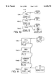
- FIG. 1 illustrates per-VC queues of ATM cells in an ATM switch according to the present invention.
- FIG. 2 illustrates data structures used to maintain the queues of FIG. 1.
- FIGS. 3 and 4 are charts illustrating the operation of an ATM switch of the present invention when a cell is received.
- FIG. 5 is a chart illustrating the operation of an ATM switch of the present invention when a cell is scheduled for transmission.
- FIG. 6 is a chart illustrating how an ATM switch of the present invention determines whether an incoming cell is to be discarded.
- FIGS. 7-11 illustrate data structures at different stages of operation of an ATM switch of the present invention.
- FIG. 12 illustrates Ethernet and ATM networks interacting according to the present invention.
- FIG. 13 illustrates a state machine in an ATM switch of the present invention.
- FIG. 14 illustrates data structures in an ATM switch of the present invention.
- FIG. 15 illustrates a state machine in an ATM switch of the present invention.
- FIGS. 16-19 illustrate data structures at different stages of operation of an ATM switch of the present invention.
- FIGS. 20 and 21 are graphs illustrating the threshold and packet discard function of an ATM switch of the present invention.
- FIG. 22 is a block diagram of a circuit used to implement the threshold and packet discard function of an ATM switch of the present invention.
- FIG. 23 illustrates a state machine for an early packet discard function in an ATM switch of the present invention.
- FIG. 24 is a block diagram showing a relationship between function blocks and databases in an ATM switch of the present invention.
- FIG. 25 is a block diagram of an ATM switch of the present invention.
- FIG. 26 shows data tables and bus signals in the ATM switch of FIG. 25.
- FIG. 27 illustrates flow of data between blocks of FIG. 25.
- FIG. 28 illustrates operations performed in different switch cycles in the switch of FIG. 25.
- FIG. 29 illustrates operations performed during an input stage of the switch of FIG. 25.
- FIG. 30 illustrates an input stage pipeline of the switch of FIG. 25.
- FIG. 31 illustrates operations performed during an output stage of the switch of FIG. 25.
- FIG. 32 illustrates an output stage pipeline of the switch of FIG. 25.
- FIG. 33 illustrates flow of data in the switch of FIG. 25.
- FIG. 34 illustrates programming of the switch of FIG. 25 done to set up a connection.
- FIGS. 35-51 illustrate registers and register fields in the switch of FIG. 25.
- FIG. 1 illustrates queues 110A, 110B, 110C of ATM cells in an ATM switch.
- ATM Asychronous Transfer Mode
- the multiplexing principle makes it possible to carry several separate data streams independently over one and the same physical medium.
- asynchronous time division multiplexing the data streams to be transmitted are converted into information units of fixed or variable length and transferred asynchronously.
- the allocation of the units of information to the different transmission channels is carried out using numerical Channel Identifiers attached to each data packet. See Kyas, "ATM networks" (1995), page 28. If the switch is a VC switch, then a separate queue 110 is allocated for cells received on a given port or sub-port and having a given VCI and a given VPI. Thus, cells 104A received on an IVC A are written to queue 110A; cells 104B received on an IVC B are written to queue 110B; cells 104C received on an IVC C are written to queue 110C.
- Scheduler 120 schedules the cells for transmission.
- a separate queue 110 is allocated for cells received on a given port or sub-port and having a given VPI.
- per-VC queuing refers both to VC switches having a separate queue for each IVC and to VP switches having a separate queue for each input VP.
- the description of VC switches below applies to VP switches if "virtual channel,, is replaced by "virtual path", except where it is obvious that such a replacement is inappropriate.
- an ATM connection can operate in a frame based operation mode (FBOM) or a non-FBOM ("normal") mode.
- FBOM frame based operation mode
- normal non-FBOM
- some connections may be FBOM connections and other connections may be normal connections. We describe the normal mode first.
- Operation of the ATM switch is divided into two stages: an input stage and an output stage.
- cells 104 are received and linked to queues 110 according to the cells' input VCs.
- the ATM switch stores a data structure described in Appendix 1 at the end of this description (before the claims).
- the data structure includes a Next Cell pointer NXT used to link the cells in queue 110.
- FIG. 2 illustrates data structures stored in the ATM switch for a single connection, and thus for a single IVC and a single queue 110.
- Each IVC is described by a respective IVC structure 210. We will sometimes call structure 210 simply an IVC.
- IVC fields are described in Appendix 2.
- WP Write Pointer
- FIG. 2 illustrates a multicast connection with three output virtual channels (OVCs) OVC 0 , OVC 1 and OVC 2 .
- OVC output virtual channels
- Each OVC is described by a respective OVC structure 220 which we will call simply an OVC.
- Fields of OVC 220 are described in Appendix 3.
- each OVC includes: 1) a Read Pointer RP pointing to the next cell to transmit on the OVC; 2) field NewHDR containing the VPI and VCI of the new header for the OVC; and 3) the number "IVC" of the respective ("parent") IVC; this number is a pointer to IVC 210.
- Appendix 4 illustrates steps performed to set up a new connection.
- Appendix 5 illustrates steps performed to add a party (an OVC) to an existing connection.
- Appendix 6 and FIGS. 3 and 4 illustrate steps performed when a new cell is received.
- FIG. 5 illustrates steps performed to transmit a cell.
- FIG. 6 illustrates steps performed to determine whether a cell is to be discarded. Appendices 4-6 and FIGS. 3-6 are discussed below.
- OVCs belonging to the same IVC may or may not be connected to different output ports or sub-ports.
- a sub-port is a logical port; a group of sub-ports share the same physical port.
- Different output VCs corresponding to the same IVC may be in different states at the same time. For example, one OVC may have finished sending all cells from respective queue 110 (i.e., the queue 110 may be empty for this OVC), while other OVCs are still sending cells from the queue.
- the cell 104 When a cell 104 has been transmitted by all OVCs corresponding to the IVC, the cell is dequeued, and the cell's memory is returned to a stack of free cell buffers.
- the counter ECNT the count of cells in the IVC queue, see Appendix 2
- each OVC 220 includes: a flag L used in FBOM to indicate whether the cell pointed to by the OVC's RP is the last cell of a frame; and a flag M indicating whether the cell pointed to by RP is a marker cell. Marker cells are used to remove OVCs, as described below.
- the fields RP, L, and M of each OVC are stored in a 20-bit field (see entry "RP" in Table 4 below).
- each cell data structure has 20 bits that contain the cell's NXT (Appendix 1) and the cell's flags L and M. L indicates whether the next cell is the last cell in a frame. M indicates whether the next cell is a marker cell.
- NXT, L, M is copied to the OVC's (RP, L, M) field in parallel.
- OVCs of a given IVC are linked in a linked list 310 (FIG. 8).
- the list 310 an IVC chain of OVCs.
- OVCs OVC1, OVC2, OVC3 belong to IVC X. These OVCs are empty. This means that either: (1) the respective queue 110 is empty, or (2) queue 110 is not empty, but all the cells in the queue have been transmitted by OVC1, OVC2, and OVC3. If queue 110 is not empty, one or more other OVCs corresponding to IVC X have not transmitted all the cells in the queue.
- IVC's Chain Head Pointer CHP (Appendix 2) points to the first OVC (OVC1) in chain 310.
- IVC's Chain Tail Pointer CTP points to the last OVC (OVC3) in chain 310.
- each PVC (per-VC controller) 1440 handles a separate set of output ports, and each PVC has its own chain 310 for the OVCs transmitting on the output ports handled by the PVC.
- Each PVC 1440 has a single background list 410 for all the IVCs. OVCs are added to list 410 in the same order as they were in respective chain 310.
- a pointer HBL Head of Background List
- a pointer TBL Tiil of Background List
- OVC3 the last OVC
- an OVC is in a chain 310 if the OVC has transmitted all the cells in queue 110 or the only cells not transmitted by the OVC are cells of a partial frame (that is, a frame that has not been completely received on the respective IVC).
- the OVC gets a full frame to transmit, the OVC is moved to respective list 410.
- each OVC structure 220 has a flag R in respective PVC 1440 to indicate whether the read pointer RP[NXT] of the next OVC is valid. See Appendix 3 and Table 4, entry IVC/NXT. Thus, as long as the NXT pointer of OVC1 points to OVC2, the R flag of OVC1 is 1 if RP of OVC2 is valid. In FIG. 8, OVC2 and OVC3 are empty, and hence the R flags in OVC1, OVC2 are 0. The R flag of OVC3 is fix" ("don't care").
- Each background circuitry goes through respective list 410, performing the following operation for each OVC in the list:
- temp -- RP -- L -- M OVC's RP, L, M
- temp -- RP -- L -- M and temp -- R are storage locations in the background circuitry in each PVC 1440.
- Each cell 104 includes a Copy Counter field CCNT (Appendix 1) which stores the number of OVCs to which the cell is to be transmitted.
- CCNT Copy Counter field
- CCNT Output Counter
- a new OVC is created and linked to the chain 310 of corresponding IVC 210 (Appendix 5, steps 1a, 1b) in respective PVC 1440.
- OVC2 was added after OVC0 and OVC1.
- Cells 104.1, 104.2 in queue 110 arrived before addition of OVC2.
- Their CCNT fields were unchanged when OVC2 was added, and these cells will not be transmitted on OVC2.
- OVC2 was added, its RP was invalid.
- Cell 104.3 is the first cell arriving after the addition of OVC2.
- Linking the new OVC to the IVC chain and incrementing the IVC's Output Counter OCNT is done as an atomic operation before a new cell (cell 104.3 in FIG. 10) is received.
- FIG. 11 illustrates removing OVC2 from a multicast connection.
- the OVC counter OCNT was n, and cells 104.1, 104.2 had already been received but had not been transmitted by any OVC. These cells will be the last cells transmitted on OVC2 before DVC2 is removed.
- a "marker” cell 104M is linked to the IVC queue. In the previous cell 104.2, flag M is set (Appendix 1) to indicate that the next cell is a marker cell. Marker cell 104M will not be transmitted by any OVC.
- Cell 104.3 is received after the marker cell, and in cell 104.3 CCNT is initialized to the new OCNT value of n-1. In marker cell 104M and preceding cells, CCNT was initialized to the old OCNT value.
- OVC2 When OVC2 reaches the marker cell 104M, OVC2 is removed from the list of active C)VCs (step 970 in FIG. 5).
- a command to remove more than one OVC is processed similarly.
- FBOM is used to multiplex several user ATM connections onto the same ATM connection. Multiplexing can be done even with user interfaces such as AAL-5 which do not require each cell to identify the cell's position in a frame or even the fact that the cell belongs to the frame. The cell's position in a frame, and the fact: that the cell belongs to the frame, are known because the cells of a frame are transmitted on an output port: or sub-port in the order in which they appear in the frame, with no intervening cells.
- AAL-5 ATM Adaptation Layer 5
- FIG. 12 illustrates multiplexing of different connections onto one ATM connection to interconnect Ethernet segments 2010.1-2010.5 through an ATM network. Traffic from Ethernet segments 2010.1, 2010.2 2010.3, 2010.4 to Ethernet segment 2010.5 is carried as follows. Each segment 2010.1-2010.4 sends Ethernet packets to respective Ethernet Interface circuit 2014.1-2014.4. Each circuit 2014.1-2014.4 converts each Ethernet packet to a frame of one or more ATM cells. Ethernet interface circuit 2014.3 sends its frames to one port of ATM switch 2040B on a virtual connection VC1. Circuit 2014.2 sends its frames to another port of switch 2040B on a virtual connection VC2. Switch 2040B queues the cells from each circuit 2014.3, 2014.2 in a separate queue. Since these cells have the same destination, switch 2040B transmits them on the same virtual connection VC3 to a port of ATM switch 2040C. The cells are transmitted in frame based operations mode, and thus different frames are not intermixed.
- Frames from Ethernet interface circuit 2014.1 travel through ATM switch 2040A to a different port of ATM switch 2040C, and arrive to switch 2040C on a different virtual connection VC4.
- Switch 2040C queues the cells received on connections VC3, VC4 in different queues, but transmits them on the same virtual connection VC5 since the cells in both queues have the same destination. The cells from both queues are transmitted in frame mode, and thus the frames are not intermixed.
- Virtual connection VC5 is connected to one port of ATM switch 2040D.
- Virtual connection VC6 from Ethernet interface circuit 2014.4 is connected to a different port of switch 2040D.
- the cells arriving on connection VC5, VC6 are queued in different queues, but transmitted on the same connection VC7 in frame mode.
- Ethernet interface circuit 2014.5 receives the cells on connection VC7, reassembles each frame into an Ethernet packet, and transmits the packet to Ethernet segment 2010.5.
- circuit 2014.5 Since each frame arrives with no intervening cells from any other frame, the reassembly performed by circuit 2014.5 is a simple task. Further, circuit 2014.5 does not require memory to store partial frames as would be the case if frames arrived intermixed. The cost of circuit 2014.5 is therefore reduced.
- interface circuits 2014 use AAL-5 ATM adaptation layer.
- FBOM allows different AAL-5 connections and different ATM connections to be multiplexed onto the same ATM connection (for example, VC4, VC3 are multiplexed onto VC5), even though AAL-5 does not insert into each frame any information, such as MID in AAL-3/4, that would indicate the cell's position in a frame or even the fact that the cell belongs to the frame. The number of virtual connections can therefore be reduced even using AAL-5.
- the FBOM operation of an ATM switch is similar to the normal-mode operation. However, in some embodiments:
- the OVC starts transmission on a frame boundary.
- an IVC may be in one of the following two states (FIG. 13), as indicated by the IVC's flag P (Appendix 2):
- the IVC queue 110 is empty or consists of one or more full frames.
- a cell is received which is not the last cell of a frame
- Each IVC has a Tail Pointer TP (Appendix 2).
- TP points to the last cell of the last full frame in respective queue 110.
- cells 104-0,1 and 104-0,2 belong to frame 0; cell 104-1,1 belongs to frame 1.
- TP WP.
- scheduler 120 When an OVC is selected for output, scheduler 120 will select the same OVC for the OVC's port or sub-port until an entire frame has been transmitted.
- the address of the cell being transmitted becomes equal to TP (FIG. 5, step 850)
- the OVC becomes empty and returns to respective chain 310 (steps 870, 874) waiting for another full frame to be received.
- the flag L (Appendix 1) of the previous cell is set to a value indicating whether the new cell is the last cell in a frame. See Appendix 6, step 1a. Also, if the respective IVC's chain 310 is not empty, the first OVC in each non-empty chain 310 gets its flag L also set to a value indicating whether the new cell is the last in a frame.
- FIG. 3 illustrates operations performed by each PVC 1440 to update an IVC's flags P and pointers TP when a cell is received.
- Each PVC 1440 keeps a copy of flag P and pointer TP.
- TP gets the cell address (step 520; see also step 2d in Appendix 6).
- Step 520 is performed, and steps 530-560 are performed as needed as described above.
- steps are performed not necessarily in the order shown or described.
- step 520 is performed in parallel with steps 530-560.
- steps 550 and 560 are performed in parallel.
- FIG. 4 illustrates updating the OVC read pointers when a cell is received.
- the IVC's R is set to 1 (step 720 and Appendix 6, step 3a-1), and
- an OVC structure 220 is in one of four states as shown in FIG. 15.
- the states are as follows:
- OVC data structure does not belong to any connection.
- the structure is free to be defined and assigned to an output virtual channel.
- Empty--the OVC is defined and linked to its parent IVC in chain 310. However there is no full frame for the OVC to transmit. In a non-FBOM connection, there is no cell for the OVC to transmit.
- Ready--the OVC is in list 410 ready to be transferred to scheduler 120.
- FBOM there is at least one full frame for the OVC to transmit.
- non-FBOM there is at least one cell for the IVC to transmit.
- Active--the OVC is off the BG list and under scheduler control. Every time the OVC is scheduled for transmission, the OVC emits one cell from the IVC queue.
- the connection When the connection is first set up, the IVC is empty, and therefore both WP and TP are undefined (invalid).
- the C bit (Chain is Ready) is set (step 1f) since the connection is set up with at least one OVC in chain 310.
- CHP and CTP point to the OVC (Appendix 4, step 1d).
- the OVC has a pointer to its parent IVC (step 2b).
- flag C is reset. This setup is done when a command "IPVC Setup connection" is executed.
- the IVC Write Pointer is updated to point to the new cell (Appendix 6, step 2a). Then, the OVC Read Pointer is updated to point to the new cell (step 3a-2), and the IVC flag R is set in respective PVC 1440 (step 3a-1).
- FIG. 5 illustrates transmitting a cell on an OVC.
- the operations of FIG. 5 are performed by the PVC 1440 maintaining the OVC, except as made clear otherwise.
- the OVC's fields RP, L, M receive the cell's NXT, L, M.
- Flag A is used in FBOM to ensure that the transmission on a new OVC starts on the frame boundary when the OVC is first added.
- the cell is transmitted (step 840).
- the PVC 1440 sends the cell address and the VPI/VCI of the cell's new header to SIF 1420 (FIG. 25) for transmission, as shown in the bottom half of FIG. 27.
- the cell address is equal to TP (step 850)
- the OVC is moved to respective chain 310 (step 880).
- the marker cell's CCNT is decremented (by SIF 1420) at step 950 or 960.
- the OVC is removed.
- connection is an atomic operation which takes place a short time after the command to add a connection is issued. We do not wait until t he entire frame is received when we add a connection.
- OVC n3 and OVC n4 are added, in that order, when the following conditions hold:
- the IVC queue consists of: a) cell 1.4 of frame 1; b) cells 2.0, 2.1, 2.2 of a full frame 2; and c) cells 3.0, 3.1 of a partial frame 3.
- OVC n0 is empty, waiting for the last cell of frame 3 to arrive. Its Read Pointer points to cell 3.0, which will be the next cell transmitted by this OVC. Thus, even though OVC n0 is empty, its RP is valid.
- OVC n1 is active, transmitting frame 2. Its Read Pointer points to cell 2.1, which will be the next cell transmitted by this OVC.
- OVC n2 is active, transmitting frame 1. Its Read Pointer points to cell 1.4.
- OVC n3 , OVC n4 transmit on ports handled by the same PVC 1440 (FIG. 25), and therefore the two OVCs are added to the same chain 310.
- the new OVCs are added at the head of IVC chain 310, and the IVC flag R is reset in respective PVC 1440.
- the RP fields of OVC n3 , OVC n4 are shaded.
- OVC n3 and OVC n4 the A bits are set.
- the RP of the head OVC n4 of chain 310 is set to point to the new cell, and the IVC's flag R is set in respective PVC 1440.
- the Tail Pointer of the IVC in each PVC is set to point to this cell and the entire IVC chain 310 is linked to the background list 410 in the respective PVC 1440. Going through the list, the background job will set the Read Pointer of OVC n3 to be equal to the Read Pointer of the OVC n4 .
- the OVC is marked to be dropped (D bit is set in respective PVC 1440).
- a marker cell is sent by the CPU to be queued in respective queue 110.
- This marker cell is constructed as a normal cell with a payload of all zeroes and a PTI field indicating the last cell of a frame.
- the marker cell's payload and PTI field are stored in a memory (not shown) used to store payloads and headers of incoming cells.
- OVC n0 is empty and waiting for frame 3 to be received. Both OVC n1 and OVC n2 are active transmitting frames 2 and 1 respectively. The D bits of OVC n1 and OVC n0 are set, indicating that these OVCs are intended for removal.
- the marker cell would be queued as the first cell of a partial frame. n particular, the L flag of cell 2.2 and the P flag of the IVC would be reset.
- FIG. 19 shows a stack of removed OVC structures in a PVC 1440.
- Pointer OSP points to the top of this stack. Every time a new OVC is removed (FIG. 5, step 970), it is added at the top of the stack.
- the switch CPU (such as CPU 1414 in FIG. 25) issues a command to remove an OVC
- the CPU marks the OVC in the CPU's database as intended for removal.
- some time may elapse before the OVC transmits the market cell and is actually removed and added to the OSP stack.
- the CPU does not get informed when the OVC is actually removed.
- the CPU reads the OSP stacks in both PVCs and marks the removed OVCs in the CPU database.
- the CPU needs an OVC to add a connection
- the CPU gets a new C)VC from the CPU's database, and thus the CPU does not need to read the OSP stacks at that point of time.
- adding a connection is a fast operation.
- the switch CPU reads the OSP to get the top OVC in the stack.
- OSP OSP is set to point to this OVC.
- a new stack of removed OVCs is formed. Newly removed OVCs are added to this new stack.
- the CPU reads OSP to get: an OVC from the new stack.
- This stack management technique has the following benefits: (1) the CPU does not need to read OSP each time the stack is to be popped; (2) zeroing OSP when OSP is read is simpler than setting OSP to point to an OVC in the stack.
- This function handles congestion in the ATM switch. In particular, this function determines the following thresholds for each queue 110:
- a marking threshold If a cell is received on an IVC when ECNT of the IVC exceeds the marking threshold, cells received on the IVC will be transmitted with an overload indication (i.e., with the PTI bit 1 set).
- a discard threshold (above the marking threshold in some embodiments). If a cell is received when ECNT exceeds the discard threshold, the cell is treated as follows:
- the early packed discard policy (EPD) is used. This means that if the cell is the first cell of a frame, the whole frame is discarded. If the cell is not the first cell in a frame, and a previous cell in the frame was not discarded, the cell is not discarded.
- EPD early packed discard policy
- a queue limit (above the discard threshold in some embodiments). If a cell is received when ECNT exceeds the queue limit, the cell is discarded.
- the marking threshold is used as follows. Each IVC structure has a flag I (Appendix 2) indicating whether the EFCI marking is enabled on the IVC (EFCI stands for Explicit Forward Congestion Indication). Each IVC structure has also a forward congestion notification flag N. When a cell is received on the IVC, the following steps are performed by SIF 1420:
- the IVC's flag I is set (that is, if EFCI marking is enabled), and the IVC's counter ECNT exceeds the marking threshold, then the IVC's flag N becomes set.
- the cell is transmitted with PTI bit 1 set (that is, with overload indication).
- the thresholds vary dynamically depending on the congestion state of the switch.
- the thresholds are set as follows. Every Input VC belongs to one of 16 classes, as indicated by the IVC field CLID (class ID; see Appendix 2). CLID is assigned when the connection is set up (Appendix 4, step 1c). In some embodiments, a separate CLID is assigned for each QoS or for a range of QoS parameters.
- the ATM switch keeps a Class Counter which is the total number of cells in all the queues 110 of this class. Thus, the class counter is the sum of all ECNT values in the class. When a cell is received, the respective Class Counter is incremented. The counter is decremented when a cell in the class is returned to the stack of free cell buffers after transmission.
- the marking, discard, and queue-limit thresholds are set separately for each class.
- the possible values of the Class Counter are subdivided into 8 regions numbered 0 through 7. Each threshold is constant in each region.
- FIG. 20 is a graph for one threshold.
- the upper limit of region 7 is the "class limit".
- the region limits are programmable per class, and thus can be different for different classes.
- a threshold is the same in two or more neighboring regions.
- the switch For each class, the switch maintains a Class Region Id variable indicating in which region the Class Counter is. The actual threshold is determined from the Class Region ID.
- the cells that have already been queued are not affected. For example, suppose that in FIG. 20 the class counter increases from region 0 to region 1. The threshold decreases from A to B. However, if a queue 110 in the class had more than B cells when the class counter reached region 1, these cells do not become a subject of any additional congestion reduction action. However, the cells received for the queue after the class counter reached region 1 can be subject to such action until the number of cells in the queue goes down below B (due to cells being transmitted).
- the upper limit of each region is equal to the lower limit of the next region.
- the upper limit 6K of region 0 is the lower limit of region 1. This is not so in FIG. 21, where neighboring regions overlap. The overlap areas are shown by hatching.
- the upper limit U0 of region 0 is higher than the lower limit L1 of region 1; the upper limit U1 of region 1 is higher than the lower limit L2 of region 2, and so on.
- the region ID changes with a hysteresis based on the direction of change of the class counter. For example, when the class counter increases from region 0, the region ID becomes 1 when the class counter reaches U0. When the class counter decreases from region 1, the region ID becomes 0 when the class counter reaches L1.
- the hysteresis prevents the region ID, and hence the thresholds, from oscillating when the class counter oscillates around a region boundary.
- FIG. 22 illustrates a circuit (part of SIF 1420) used to determine class counters and region IDs. This circuit is invoked every time a cell is received or a cell memory is released.
- CLID table 1110 stores the CLID fields of IVCs 210. Table 1110 is indexed by the IVC number. The IVC number is shown as "IVC" in FIG. 22.
- CLID class ID
- the output of register 1114 is connected to inputs of class counter table 1120 and region ID table 1130.
- Tables 1120 and 1130 are indexed by the class ID.
- Class counter table 1120 writes the class counter ("CLC") to circuit 1134.
- Region ID table 1130 writes the region ID ("RID”) to circuit 1140.
- Circuits 1140 and 1114 provide respectively the region ID and the class ID to lower limit table 1150, upper limit table 1160, and threshold table 1170.
- Table 1150 provides the lower limit of the region to comparator 1180.
- Table 1160 provides the upper limit to comparator 1190.
- Table 1170 provides the marking, discard, and queue limit thresholds to comparator 1196.
- the IVC number "IVC" is delivered as an index to table 1194 which stores the ECNT fields of IVC structures 210 (Appendix 2).
- the output ECNT of table 1194 is provided to comparator 1196.
- Comparator 1196 compares ECNT with each of the three thresholds from table 1170 and generates signals indicating whether any thresholds are exceeded. These signals are provided to a circuit (not shown; part of SIF 1420) that determines whether the cell is to be discarded, transmitted with an overload indication, or transmitted without an overload indication.
- That circuit includes circuitry of FIG. 6 and the EPD state machine of FIG. 23, which are described below. That circuit provides a signal to circuit 1134 to indicate whether the cell is received and the class counter should be incremented.
- Circuit 1134 also receives a signal (not shown) indicating whether the cell is being released from the memory and the class counter should be decremented. Circuit 1134 increments or decrements the class counter accordingly or leaves the class counter unchanged. The new value of the class counter is written back to its slot in table 1120 and is delivered to comparators 1180, 1190.
- Each of comparators 1180, 1190 receives signals (not shown) indicating whether the class counter was incremented or decremented by circuit 1134. If the class counter was decremented, and is less than the lower limit, comparator 1180 sends a signal to circuit 1192 that the region ID is to be decremented. If the class counter was incremented and is greater than the upper limit, comparator 1190 sends a signal to circuit 1192 that the region ID is to be incremented. Circuit 1192 signals circuit 1140 whether the region ID is to be incremented or decremented or to remain unchanged. Circuit 1140 changes the region ID if needed and writes it back to table 1130.
- EPD state machine of FIG. 23 is provided in SIF 1420 for each Input VC.
- EPD can be disabled.
- the EPD is enabled or disabled on a per-IVC basis.
- FIG. 6 shows operations performed to determine if an incoming cell is to be received or discarded.
- the operations are performed by SIF 1420 unless made clear otherwise. If the switch memory for storing the cells is full (step 1270), the cell is discarded (step 1272). This is done by switch controller (SWC) 1410 (FIG. 25) regardless of any marking, discard or queue-limit threshold.
- SWC switch controller
- SIF 1420 tests if the cell's class is full, i.e., the class counter exceeds the class limit. If so, the cell is also discarded.
- step 1276 If the corresponding IVC queue is full (step 1276), that is, ECNT is greater than the IVC's queue limit, as determined from the output signals of comparator 1196 (FIG. 22), then the cell is discarded.
- the IVC's EPD state machine is in the state "Frame Discard” (step 1280), then the cell is discarded. If the EPD state is "Start of Frame” (step 1285), and the cell is received if the EPD state is not “Start of Frame” (i.e., if the EPD state is "Frame Receive”).
- step 1278 If at step 1278 the EPD function is disabled, then the cell is received if, and only if: (1) ECNT does not exceed the discard threshold (step 1286), or (2) the CLP bit in the cell's input header is 0 (step 1287).
- FIG. 24 shows the relationship between functional blocks and databases in one embodiment of the ATM switch.
- Cell database 1310 includes cells 104.
- IVC database 1320 includes IVC structures 210.
- OVC database 1330 includes OVC structures 220.
- the switch circuitry includes input function block 1340, output function block 1350, background. (BG) function block 1360, and scheduler function block 120. The relationship between the function blocks and the databases is described in the following Table 3.
- Switch controller (SWC) 1410 is connected to CPU 1414, I/O ports 1418, and SIF (Switch Interface) 1420.
- SIF 1.420 is connected to interconnect bus 1430.
- Bus 1430; is connected to one or more PVCs (per-VC controllers) 1440.
- PVCs per-VC controllers
- Each PVC 1440 is connected to a respective SCM (scheduler) circuit 1450.
- Scheduler circuits 1450 are par-t of scheduler 120 (FIG. 1).
- ports 1418 include 32 input ports and 32 output ports.
- the switch has two PVCs. One PVC 1440 handles the 16 even output ports, and the other PVC handles the 16 odd output ports.
- each of circuits 1410, 1418, 1420, 1430, 1440 and 1450 is a separate integrated circuit.
- SIF 1420 stores the following tables: ECNT, CLID, WP, OCNT, LINK, CCNT, OVCT.
- PVC 1440 stores the tables CHP/CTP, IVC/NXT, RP, TP. These tables are described in Table 4 below.
- the RP tables store information only for OVCs corresponding to the output ports handled by the PVC.
- each PVC 1440 has CHP and CTP pointers and R, C and H flags for each IVC.
- Each chain 310 contains the OVCs that transmit on the output ports handled by the respective PVC.
- each PVC updates its IVC and OVC fields as described above.
- TP, P and F have the same values in each PVC 1440.
- FIG. 27 illustrates the flow of data between blocks of FIG. 25.
- SWC 1410 receives and transmits cells on the network via I/O ports 1418.
- SWC 1410 receives marker cells from CPU 1414.
- SWC 1410 sends to SIF 1420 the address of the cell in a switch memory (not shown) and the ID of the respective IVC.
- the IVC ID also referred to herein as the IVC number, is the same number as stored in OVC 220 (Appendix 3).
- SIF 1420 links the cell into the corresponding queue 110, and updates the ECNT counter.
- SIF 1420 when the connection is being established or an OVC is being added, is to generate the new header NewHdr for the new OVC.
- SIF 1420 transmits the cell address and the IVC ID to both PVCs 1440.
- PVCs 1440 update OVC fields and perform the operations shown in FIGS. 3 and 4 as described above. If an OVC becomes ready when the cell is received, the respective background job sends the OVC ID to respective SCH 1450 (the transfer PVC ⁇ SCH).
- the OVC ID serves as a pointer to the OVC. For those OVCs that were active when the cell was received, the transfer PVC ⁇ SCH is not performed.
- SCH 1450 Each time SCH 1450 schedules a cell on an OVC for transmission, SCH 1450 sends the OVC ID to respective PVC 1440, as shown in the bottom half of FIG. 27.
- PVC 1440 updates the OVC fields as shown in FIG. 5, and sends the OVC ID and the cell address to SIF 1420.
- PVC 1440 compares the IVC TP with th,e cell address (step 850 in FIG. 5) to determine if the OVC becomes empty. If the OVC becomes empty, PVC 1440 signals respective SCH 1450 that the OVC is empty, and links the OVC to respective chain 310.
- SIF 1420 removes the cell from respective queue 110 if needed, updates ECNT, and sends the cell address and the new header to switch controller 1410.
- Controller 1410 transmits the cell on one of ports 1418 or to CPU 1414.
- the entire operation is performed in several switch cycles as shown in FIG. 28.
- the background (BG) job may take more than one switch cycle.
- BG background
- the incoming cell goes through several processing stages as shown in FIG. 29.
- LUT and ITT are tables described in U.S. patent application Ser. No. 08/657,835, "Cell Routing in ATM Networks", filed May 31, 1996 by Alex Joffe, now U.S. Pat. No. 5,936,959, issued on Aug. 10, 1999, and hereby incorporated herein by reference.
- the function and input/output parameters of each processing stage are described in the following Table 6:
- the Write Pointer (WP) is written back during the output stage of the switch.
- ATTR stands for cell attributes (see the aforementioned U.S. pat. application Ser. No. 08/657,835), now U.S. Pat. No. 5,936,959.
- STACK is a stack of free cell buffers in a shared memory.
- FIG. 33 This operation is initiated by CPU 1414 to write data to SIF 1420 or a PVIC 1440.
- SIF 1420 and PVC 1440 has a control memory to store data such as data in the tables of FIG. 26.
- control memories 1510, 1520 of SIF 1420 and a PVC 1440 are shown outside the SIF and PVC for ease of illustrating Write Control Memory operations.
- a Write Control Memory operation includes the following steps (the step numbers are circled in FIG. 33):
- CPU 1414 writes registers RO and CMR in SWC 1410. These registers specify the command as described below.
- SWC 1410 transfers the contents of registers CMR and R0 through bus ttd[31:0] to SIF 1420 during two clock cycles.
- SIF 1420 transfers the contents of registers CMR and RO to respective PVC 1440 during two clock cycles using concatenated vc -- bus[15:0] and cp -- bus[15:0].
- SIF 1420 and PVC 1440 decode the command and write data to specified locations in their control memories.
- This operation includes the following steps (steps number appear in squares in FIG. 33):
- CPU 1414 writes registers RO and CMR in SWC 1410.
- SWC 1410 transfers the contents of registers CMR and RO through bus ttd[31:0] to SIF 1420 during two clock cycles.
- SIF 1420 reads data from its control memory 1510.
- CPU 1414 reads the result from register RO.
- This operation includes the following steps (step numbers are in pentagons in FIG. 33):
- CPU 1414 writes registers RO and CMR in SWC 1410.
- SWC 1410 transfers the contents of registers CMR and R0 through bus ttd[31:0] to SIF 1420 during two clock cycles.
- SIF 1420 transfers the contents of register CMR to respective PVC 1440 using concatenated vc -- bus[15:0] and cp -- bus[15:0].
- PVC 1440 transfers its result to SIF 1420.
- CPU 1414 reads the result from register RO.
- connection is set up using the following steps:
- Step 1 Setup the New Header by using the "Write -- Ext -- Table -- Reg" command.
- Step 2 Issue the "PVC Setup Connection” command (described below).
- Step 3 Issue the switch controller "Setup Connection" command described in "ATMS2003B Switch Controller 1 ⁇ WHITE ⁇ ” (MMC Networks, Inc. of California, document MMC 95-0003, 1995), incorporated herein by reference, at page 18.
- connection is added in the following two steps:
- Step 1 Setup the New Header by using the "Write -- Ext -- Table -- Reg" command.
- Step 2 Issue the "PVC Add Connection” command.
- This section describes the SWC registers CMR and R0 for different commands.
- Address is the address in a table or internal registers being read or written.
- Data is data being written.
- This command is used in a Remove Connection operation. It is similar to a Queue Cell command described in "ATMS2003B Switch Controller 1 ⁇ WHITE ⁇ " (cited above), at page 19.
- Bits CMR[25] and CMR [24] store OCNT [9] and OCNT [8].
- PTI PTI field of the cell's header (should be last cell in frame, i.e. PTI bit 1 should be set.
- the SIF table format is shown in FIG. 39.
- the PVC table format is shown in FIG. 40.
- This register controls the operation of per-VC queuing.
- SIF 1420 is implemented in 3 chips SIF -- 1, SIF -- 2, SIF -- 3. Accordingly, there are three VER -- i registers, one per SIF device (VER -- 1 corresponds to SIF -- 1, and so on).
- class counter registers there are 16 class counter registers (one for each class) in SIF 1420. These counters are cleared on reset and incremented every time a cell is received in the class. A class counter is decremented when a cell in the class is transmitted and released to the free cell buffer stack. The user can read these registers any time during the operation. Writing to the registers is supported for testing only and should not be done in normal operation.
- the RID fields of CLC registers form region ID table 1130 of FIG. 22.
- the CLC fields form table 1120 of FIG. 22.
- Each RID field is cleared on reset and updated every time the Class Counter crosses a region boundary.
- Region Threshold Registers 8 for each class, 1 register for each region. These registers form threshold table 1170 of FIG. 22. These registers should be initialized by the user.
- All thresholds have a granularity of 16 cells.
- the maximum size of queue 110 is 16K-1 cells, which is a 14-bit space.
- the four LSBs of each threshold are 1111. Therefore, the minimum value of each threshold is fifteen (00 -- 0000 -- 0000 -- 1111 binary), and the maximum value is 16K-1 (11 -- 1111 -- 1111 -- 1111 binary).
- Region Limits Registers 8 for each class, 1 register for each region. These registers form tables 1150, 1160 in FIG. 22. These registers should be initialized by the user.
- Both limits have a granularity of 64 cells.
- the maximum class size is 64K-1 cells, which is a 16-bit space.
- the LSBs of each upper limit are 111111, and the LSBs of each lower limit are all zeros. Therefore, the minimum upper limit is 63 (00 -- 0000 -- 0000 -- 111111 binary), and the maximum upper limit is 64K-1 (11 -- 1111 -- 1111 -- 11111 binary).
- the minimum lower limit is zero (00 -- 0000 -- 0000 -- 000000 binary), and the maximum lower limit is 64K-64 (11 -- 1111 -- 1111 -- 000000 binary).
- SIF 1420, each PVC 1440 and each SCH 1450 is a separate integrated circuit (separate chip). Such construction enables one to provide per-VC queuing as an additional function to an existing switch controller 1410.
- the SIF, PVC and SCH chips provide the following features:
- Each Input VC may have up to 16 K cells
- Each Input VC may belong to one of the 16 Classes.
- Output VCs can be associated with one Input VC (multicast). Several such OVCs may belong to the same output port.
- Port 32 (CPU port, handled by the even-ports PVC) has its own OVCs. For these OVCs, a new header is not generated. Instead, the CPU is provided with the IVC id.
Abstract
Description
              TABLE 1
______________________________________
#    from      to        condition
______________________________________
1    Not Defined
               Empty     OVC is added to IVC chain by
                         CPU request
2    Empty     Ready     In FBOM, the last cell of a
                         first full frame has arrived.
                         In normal mode, a new cell has
                         arrived on the IVC. OVC is
                         waiting for background job.
3    Ready     Active    OVC is transferred to
                         scheduler by background job
4    Active    Not Defined
                         OVC is removed by CPU request
                         (after transmission of marker
                         cell)
5    Active    Empty     the cell with a pointer equal
                         to Tail Pointer has been
                         transmitted on OVC
______________________________________
              TABLE 2
______________________________________
from       to      condition    action
______________________________________
1     Start of Start of
                       last cell of a
                                  receive if IVC
      Frame    Frame   frame arrived
                                  queue is at or
                                  below discard
                                  threshold, discard
                                  otherwise
2     Start of Frame   non-last cell
                                  receive the cell
      Frame    Receive arrived and IVC
                       queue at or below
                       discard threshold
3     Frame    Start of
                       last cell arrived
                                  receive the cell
      Receive  Frame
4     Frame    Frame   non-last cell
                                  receive the cell
      Receive  Receive arrived
5     Frame    Tail    cell was   discard the cell
      Receive  Discard discarded for
                       some reason (e.g.
                       memory full or
                       queue limit is
                       exceeded)
6     Tail     Tail    non-last cell
                                  discard the cell
      Discard  Discard arrived
7     Tail     Start of
                       last cell arrived
                                  receive the cell
      Discard  Frame
8     Start of Frame   cell arrives when
                                  discard the cell
      Frame    Discard IVC queue is
                       above discard
                       threshold or cell
                       was discarded for
                       some reason
9     Frame    Frame   non-last cell
                                  discard the cell
      Discard  Discard arrived
10    Frame    Start of
                       last cell arrived
                                  discard the cell
      Discard  Frame
______________________________________
              TABLE 3
______________________________________
Function
block
name    DB        Functions
______________________________________
Input   Cell DB   Uses cell's NXT field to link cell; sets
                  CCNT = OCNT
Input   IVC DB    Uses and updates WP and ECNT; checks
                  against thresholds; reads CHP and CTP
Input   OVC DB    Moves IVC chain to BG list using NXT
                  fields; updates RP of the first OVC in
                  the chain
BG      OVC DB    Traverses background list using OVCs'
                  NXT fields; sets RPs for OVCs in the
                  list
BG      Scheduler Transfers OVCs which are ready for
                  rescheduling
Scheduler
        Output    Indicates which OVC to transmit; gets
                  back indication if the OVC is empty
                  and/or port is full
Output  Cell DB   Finds the next cell to transmit using
                  cell's NXT field
Output  IVC DB    Checks for OVC Empty (compares OVC RP
                  with IVC TP) and moves OVC to IVC chain
                  if the OVC is empty
Output  OVC DB    Updates RP; reads NewHdr to generate New
                  Header; reads IVC field to find the
                  parent IVC
______________________________________
              TABLE 4
______________________________________
Table   Name     Addressed by
                            Bit #
                                 Functions
______________________________________
SIF Tables
ECNT    Entry    IVC id          This table has an
        Counter                  entry for each
                                 Input VC and it
                                 consists of the
                                 following:
                            13:0 ECNT - Entry
                                 Counter (14 bits)
                            15:14
                                 EST - EPD State (2
                                 bits)
                            16   M - Marker bit
                            17   N - Forward
                                 Congestion
                                 Notification flag
CLID    Class Id IVC id          This table has an
                                 entry for each
                                 Input VC and it
                                 consists of the
                                 following:
                            3:0  CLID - Class ID (4
                                 bits)
                            4    E - EPD Enable
                            5    I - EFCI Marking
                                 Enable
WP      IVC      IVC id          IVC Write Pointer
        Write               17:0 WP - Write Pointer
        Pointer
OCNT    Output   IVC id          Number of OVCs
        Count                    connected to this
                                 IVC
                            25:16
                                 OCNT - Output Count
LINK    Link     Cell Addr       This table is used
        Pointers                 to link cells into
        table                    IVC Queue (entry
                                 for each cell)
                            17:0 NXT - Link Pointer
                                 (to next cell in
                                 queue)
                            18   L - Next cell is
                                 last cell in frame
                            19   M - Next cell is
                                 marker cell
CCNT    Copy     Cell Addr       One entry per cell.
        Count                    Number of copies of
                                 the cell to
                                 transmit
                            9:0  CCNT - Copy Counter
OVCT    Output   OVC id          The Output VC table
        VC Table                 has an entry for
                                 each OVC and it
                                 consists of the
                                 following:
                            43:16
                                 NewHDR - New Cell
                                 Header VPI/VCI
                            44   VP - Virtual Path
                                 connection flag
                            15:0 IVC - parent Input
                                 VC for this OVC
PVC Tables
CHP/CTP Chain    IVC id          Chain Pointers
        Head and                 entry for each IVC
        Tail                15:0 CHP - Chain Head
        Pointers                 Pointer
                            16   R - Read Pointer
                                 Valid
                            15:0 CTP - Chain Tail
                                 Pointer
IVC/NXT Input VC OVC id          An entry for each
        and Next                 OVC (17 bits) as
        OVC                      follows:
        field               15:0 IVC - parent IVC
                            16   D - Delete OVC
                            17   A - Add OVC
                            15:0 NXT - Next OVC (in
                                 chain or BG list)
                            16   R - Read Pointer
                                 valid (for Next
                                 OVC)
RP      Read     OVC id          An entry for each
        Pointer                  OVC (16 bits)
                            17:0 RP - Read Pointer
                            18   L - RP points to
                                 last cell in frame
                            19   M - RP points to
                                 marker cell
TP      Tail     IVC id          An entry for each
        Pointer                  IVC.
                            17:0 TP - Tail Pointer
                            18   C - Chain is Ready
                            19   H - Hold
                            20   P - Partial Frame
                            21   F - Frame mode
______________________________________
TABLE 5
______________________________________
(signals)
Symbol Width I/O Function
______________________________________
Switch Controller Interface
MEMA 16 I/O Memory Address
During the Input stage, these signals are
samples by the SIF. In the Output stage
SIF will drive this bus in case when a
cell is transmitted from PVC.
TTD 32 I/O Translation Table Data
In the Input stage this bus is used by SIF
to get an IVC identifier (OPT pointer).
In the Output stage this bus is driven by
the SIF with a New Header information
when a cell is transmitted from PVC.
This bus is also used to transfer commands
to PVC.
STKU 1 I Top Of Stack Updated
During Input stage this signal indicates
that cell is received (i.e. free buffer is
taken from stack of free cell buffers).
During Output stage this signal indicates
that cell is returned to the Stack
TXST 3 I Transmit State
These three signals indicate the internal
decision of which source is selected
during the following output cycle:
000-Queue # 0 of the port is selected
001-Queue # 1 of the port is selected
010-Queue # 2 of the port is selected
011-Queue # 3 of the port is selected
100-the Multicast Output table entry
is selected
101-CPU cell is selected
110-Port Access Command
111-there is no cell to transmit
SIF will force its own cell in case when
the TXST is 001, 010, 011, or 111.
IEXC 2 O Input stage External Control
These two signals provide means for
external control logic to override
decisions of Switch controller during the
Input stage, as follows
00 - no override
01 - don't link to queue
10 - not used
11 - discard input cell (don't
update Top.sub.-- of.sub.-- Stack)
OEXC 2 O Output stage External Control
These two signals provide means for
external control logic to override
decisions of Switch controller during the
Output stage, as follows
00 - no override
01 - release MEMA bus
10 - reserved
11 - release MEMA bus and don't
release cell memory to stack of free
cell buffers
SIF is using OEXC=11 to force its own
cell for transmission.
VCR.sub.-- PE
1 I Valid Cell Received/Port Empty
During Input stage this signal means
"Valid Cell Received"
During Output stage, means "Port Empty"
EXSTKU 1 O External Stack Update
SIF will set this signal in case when
currently transmitted cell should be
returned to the stack of free cell buffers
CCPU.sub.-- PI
1 I Cell for CPU/Port Interrupt
During Input stage, means Received Cell
should be directed to CPU. SIF is using
this signal to qualify input cell.
PTI 3 I PTI field of received cell's header
CLPI 1 I CLP bit of received cell's header
General I/F
QFULL 1 O Queue Full
This signal is asserted when the
destination IVC queue is full.
QDTH 1 O Queue Discard Threshold
This signal is asserted when the
destination IVC queue reached its Discard
Threshold.
QMTH 1 O Queue Marking Threshold
This signal is asserted when the
destination IVC queue reached its Marking
Threshold.
CLST 3 O Class State
These signals indicate the Class Region ID
when cell is received.
CLFL 1 O Class Full
This signal indicates that the Class is
Full.
Interconnect Bus
CP.sub.-- BUS
18 I/O Cell pointer Bus
This bus is used to transfer Cell pointer
(cell address) to/from PVC.
NCP.sub.-- BUS
18 I/O Next Cell Pointer Bus
This bus is used to transfer Next Cell
pointer to PVC during the Output stage.
Currently not used during the Input stage.
VC.sub.-- BUS
16 I/O VC Bus
This bus is used to transfer IVC/OVC id
to/from PVC.
During the Input stage this bus is driven
by SIF and has IVC id. During the Output
stage this bus is driven by PVC and has
OVC id.
VALID 1 I/O Valid Cell flag
This bit is used in conjunction with
CP.sub.-- BUS to indicate that the cell is valid.
PBUSY 1 I/O Port Busy
This signal is driven by the SIF during
the Output stage. When set, it indicates
that Output port is busy, therefore cell
was not transmitted.
MARKER 1 I/O Cell Marker
When driven by the SIF during the Input
stage this signal identifies the Marker
cell.
During the Output stage this signal is
provided by PVC and it instructs the SIF
(together with the Last bit) to discard
the cell.
LAST 1 O Last Cell in frame
This bit identifies the Last Cell in frame
during the input stage.
During the output stage it is used in
conjunction with Cell Marker bit as
follows:
M L
0 0 - normal (non-marker) cell
transmit
0 1 - normal cell drop
1 0 - Marker Cell transmit
1 1 - Marker Cell drop
Scheduler (SCH) Interface
OVC 16 I/O OVC id
This bus is used to transfer OVC id
between PVC and SCH.
PVC.sub.-- VALID
1 O OVC Valid
This signal indicates the validity of OVC
bus to Scheduler.
SCH.sub.-- VALID
1 I OVC Valid
This signal indicates the validity of OVC
bus to PVC.
EMPTY 1 O OVC Empty
This signal is a feedback to Scheduler
which indicates that OVC is empty after
transmitting the last cell.
FULL 1 O Port Full
This signal is asserted when the output
port is full and it is not ready to get
another cell.
READY 1 I Scheduler Interface Ready
This signal indicates that the Scheduler
is ready to get a new OVC from the PVC.
FEMPTY 1 o Last Cell of a Frame
______________________________________
              TABLE 6
______________________________________
Stage  Input     Output     Function
______________________________________
Lookup Input cell
                 IVC id     Cell's header lookup
Store  Input cell
                 IVC id     Store the cell in the data
       IVC id    Cell address
                            memory
                 Cell copy  Update Top of Stack of
                 counter    free cell buffers
                 (CCNT)     Read IVC data base [SIF]
                            Check the IVC queue
                            fullness [SIF]
                            Update IVC Write Pointer
                            [SIF]
Link   IVC id    IVC id     Link cell to IVC queue
       Cell      Cell address
                            [SIF]
       address              Update the cell copy
       Cell copy            counter [SIF]
       counter
Update IVC id               Update IVC Tail Pointer &
       Cell                 Flags [PVC]
       address              Update OVC Read Pointer
                            and link OVC chain to BG
                            list [PVC]
______________________________________
              TABLE 7
______________________________________
Stage    Input      Output     Function
______________________________________
Find Cell
         OVC id     OVC id     Find RP and the
         (from      IVC id     parent IVC of the
         scheduler) Cell address
                               given OVC [PVC]
Check OVC
         OVC Id     IVC id     Compare the cell
         IVC id     OVC id     address to TP [PVC]
         Cell address
                    Cell address
                               Link OVC to parent
                    New Header IVC chain if empty
                               [PVC]
                               Find the New Header
                               for the cell [SIF]
                               Update RP [PVC]
Send     IVC id     IVC id     Read Cell data
         OVC id     Cell address
                               Generate New Header
         Cell address
         New Header
Update   IVC id                Update the cell CCNT
         Cell Address          [SIF]
                               Release cell to
                               stack if the last
                               copy [SIF]
                               Update the IVC ECNT
                               [SIF]
______________________________________
              TABLE 8
______________________________________
Table     Field           Value
______________________________________
Switch Controller
LUT       CT              =01,10,11
          ITT Base Address
                          Pointer to ITT block
ITT       V - valid       =1
          S,E,O - OAM flags
                          depends on OAM
                          processing
          FM - FCN mode   =0
          DM - Discard mode
                          =0
          Queue Number    1011.sub.-- 1111
          M - multicast   IVC[15]
          OPT pointer (IVC)
                          IVC[14:0]
SIF
OCNT      OCNT - output count
                          =1
ECNT      ECNT - entry counter
                          =0
          EST - EPD State =0 ("Start of Frame")
          M - marker      =0
          N - Fwrd Cong. Notif.
                          =0
CLID      M - marker      =0
          N - Fwrd Cong. Notific.
                          =0
          CLID - class id =class (0-15)
          E - EPD Enable  =appropriate value
          I - EFCI Marking En.
                          =appropriate value
WP        WP - Write Pointer
                          don't care
OVCT      IVC             IVC id
          VP              VP connection flag
          NewHdr          Output Cell Header
                          (VPI/VCI)
PVC that handles the output port of the OVC being added
(unless mentioned otherwise)
TP        C - Chain is Ready
                          =1 (0 in the other
                          PVC)
          R - Read Pointer Valid
                          =0
          P - Partial Frame
                          =0 in both PVCs
          H - Hold        appropriate value (in
                          both PVCs)
          F - Frame mode  appropriate value (in
                          both PVCS)
          TP - tail pointer
                          don't care
CHP/CTP   CHP             =OVC id
          CTP             =OVC id
RP        RP              don't care
          M               don't care
          L               don't care
IVC/NXT   A - Add OVC     =0
          D - Delete OVC  =0
          IVC             IVC id
          R - Read Pointer Valid
                          don't care
          NXT             don't care
______________________________________
              TABLE 9
______________________________________
Table     Field          Value
______________________________________
SIF
OCNT      OCNT - output count
                         =Current count+1
OVCT      IVC            IVC id
          VP             VP connection flag
          NewHdr         Output Cell Header
PVC handling the OVC's output port
TP        C - Chain Valid bit
                         =1
CHP/CTP   CHP            OVC
CHP/CTP   CTP            if (prev C==0) OVC else
                         don't touch
IVC/NXT   A - Add OVC    =1 (note)
          D - Delete OVC =0
          IVC            IVC id
          R - Read Pointer Valid
                         don't care
          NXT            prev CHP
______________________________________
              TABLE 10
______________________________________
DID (Device ID)      SIF
______________________________________
0ii0 (ii = PVC id)   PVC Even
                     (PVC handling
                     even output
                     ports)
0ii1                 PVC Odd
1000                 SIF
other                Reserved
______________________________________
TABLE 11 ______________________________________ TID (Table ID) SIF PVC ______________________________________ 0000CCNT TP 1000 CCNT aboveReserved 128K 0001LINK RP 1001 LINK aboveReserved 128K 0010WP CTP 0011 NewHdr CHP (OVCT) 0100 IVC (OVCT) Reserved 0101CLID Reserved 0110ECNT IVC 0111 OCNT NXT 1010-1110 Reserved Reserved 1111 Internal Regs Internal Regs ______________________________________
              APPENDIX 1
______________________________________
Data Cell
 In addition to cell payload and attributes the ATM
switch has the following data fields for each cell:
______________________________________
NXT           (18 bits) Next Cell Pointer. Used to
              link cells together.
CCNT          (10 bits) Copy Counter
FLGS          Cell Flags, including:
         L - next cell (pointed to by NXT) is the last
          cell in a frame.
         M - next cell (pointed to by NXT) is a marker
          cell
______________________________________
              APPENDIX 2
______________________________________
The IVC data structure has the following fields:
______________________________________
WP           (18 bits) Write Pointer. The address of
             the last cell in the IVC Queue.
TP           (18 bits) Tail Pointer. The address of
             the last cell in the IVC Queue (Normal
             Mode) or the last cell in the last full
             frame in the IVC Queue (FBOM).
CHP          (16 bits) Chain Head Pointer. The
             pointer to the first Output VC in the
             chain.
CTP          (16 bits) Chain Tail Pointer. The
             pointer to the last Output VC in the
             chain.
ECNT         (14 bits) Entry Counter. Number of
             cells in the queue for this IVC.
OCNT         (10 bits) Output Counter. Number of
             Output VCs which belong to this IVC.
CLID         (4 bits) Class Id.
FLGS         IVC Status & Control Flags, such as:
        F     Frame mode (0 -Normal; 1-FBOM)
        C     Chain is Ready (0-Empty; 1-Ready)
        R     Read Pointer RP of the first (head)
              OVC in the IVC's chain is Valid
              (0-not Valid; 1-Valid)
        P     Partial Frame (0-Full frame/empty;
              1-Partial frame)
        EST   EPD State (2 bits)
              00 - Start of Frame
              01 - Frame Receive
              10 - Frame Discard
              11 - Tail Discard
        E     EPD Enable (0-Disable, 1-Enable)
        I     EFCI Marking Enable (0-Disable,
              1-Enable)
        N     Congestion Notification
        M     Marker Bit (set when Marker Cell is
              linked to the Queue and reset when
              the Marker Cell is removed)
        H     Hold Bit (when set this bit
              inhibits the Chain transfer to BG
              list)
______________________________________
              APPENDIX 3
______________________________________
The OVC data structure has the following fields:
______________________________________
RP          (18 bits) Read Pointer. The Address of
            the next cell to transmit on the OVC.
NewHdr      (28 bits) New Cell Header.
NXT         (16 bits) Next OVC Pointer. Used to
            link OVCs together.
IVC         (16 bits) Input VC. Number of parent
            IVC.
FLGS        OVC Status & Control Flags, such as:
A           OVC (for Multicast Party Addition).
            0-normal, 1 added.
D           Drop connection flag.
R           Read Pointer is Valid for OVC pointed to
            be NXT of present OVC. 0-not valid, 1-
            valid.
L           Read Pointer points to the last cell of
            a frame
M           Read Pointer points to a marker cell
V           VP connection flag (0 - VC; 1 - VP)
______________________________________
              APPENDIX 4
______________________________________
Setting up a connection
______________________________________
1.       IVC set up.
1a.      OCNT = 1 (for a single OVC).
1b.      ECNT = 0 (0 cells in the queue).
1c.      CLID = class id (0 through 15).
1d.      CHP, CTP = OVC number (pointer to OVC
         structure).
1e.      F = frame mode (1 means FBOM, 0 means normal
         mode).
1f.      C = 1.
1g.      R = 0.
1h.      P = 0.
1i.      EST = 00 ("Start of Frame")
1j.      E = appropriate value (specified by CPU).
1k.      I = appropriate value (specified by CPU).
1l.      H = appropriate value.
1m.      M = 0.
2.       OVC set up.
2a.      NewHdr = new header VPI/VCI.
2b.      IVC = pointer to IVC.
2c.      A = 0.
2d.      D = 0.
2e.      V = 0 if VC connection, 1 if VP connection.
______________________________________
              APPENDIX 5
______________________________________
Adding a party to a connection
______________________________________
1.         In IVC:
1a.        CHP = pointer to new OVC.
1b.        CTP: if IVC's C == 0 (no chain), then
           CTP = pointer to new OVC
           else CTP is unchanged.
1c.        Increment OCNT.
1d.        C = 1.
1e.        R = 0.
2.         In new OVC:
2a.        NewHdr = new header.
2b.        IVC = pointer to IVC.
2c.        A = 1 if P == 1, A = 0 if P == 0.
2d.        D = 0.
2e.        V = 0 if VC connection, 1 if VP connection.
2f.        NXT = previous value of CHP.
______________________________________
              APPENDIX 6
______________________________________
Receiving a new cell
______________________________________
1.   In cells:
1a.  if the new cell is not the only cell in the
     queue, then:
if FBOM and this is the last cell in the
frame,
       L = 1 in the previous cell
       else L = 0 in the previous cell.
1b.  CCNT = IVC's OCNT.
2.   In IVC:
2a.  WP = pointer to new cell.
2b.  Increment ECNT.
2c.  If F == 1 (FBOM), then
2c-1.    if L == 1 then P = 0
         else if P == 1 then skip steps 2d-2e
         else
2c-2.      P = 1; skip steps 2d-2e.
2d.  If F == 0 (not FBOM), or
     if F == 1 and cell is the last in a frame,
     then TP = pointer to cell.
     Otherwise TP is unchanged.
2e.  If C == 1 and H == 0, then
2e-1.    C = 0.
2e-2.    Move IVC chain to background list.
3.   In OVC:
3a.  If IVC's C == 1 and IVC's R == 0, then
3a-1.    IVC's R = 1.
3a-2.    RP[CHP] = pointer to cell.
         Set L[CHP], M[CHP] to
         appropriate values.
______________________________________
Claims (62)
Priority Applications (5)
| Application Number | Priority Date | Filing Date | Title |
|---|---|---|---|
| US08/706,104 US6128278A (en) | 1996-08-30 | 1996-08-30 | Cell queuing in ATM switches |
| EP97939513A EP0864215A1 (en) | 1996-08-30 | 1997-08-28 | Cell queuing in atm switches |
| PCT/US1997/014821 WO1998009409A1 (en) | 1996-08-30 | 1997-08-28 | Cell queuing in atm switches |
| JP10511759A JPH11504793A (en) | 1996-08-30 | 1997-08-28 | Cell queuing in ATM switches |
| JP2001317004A JP2002164933A (en) | 1996-08-30 | 2001-10-15 | Cell queuing in atm switch |
Applications Claiming Priority (1)
| Application Number | Priority Date | Filing Date | Title |
|---|---|---|---|
| US08/706,104 US6128278A (en) | 1996-08-30 | 1996-08-30 | Cell queuing in ATM switches |
Publications (1)
| Publication Number | Publication Date |
|---|---|
| US6128278A true US6128278A (en) | 2000-10-03 |
Family
ID=24836238
Family Applications (1)
| Application Number | Title | Priority Date | Filing Date |
|---|---|---|---|
| US08/706,104 Expired - Lifetime US6128278A (en) | 1996-08-30 | 1996-08-30 | Cell queuing in ATM switches |
Country Status (4)
| Country | Link |
|---|---|
| US (1) | US6128278A (en) |
| EP (1) | EP0864215A1 (en) |
| JP (2) | JPH11504793A (en) |
| WO (1) | WO1998009409A1 (en) |
Cited By (18)
| Publication number | Priority date | Publication date | Assignee | Title |
|---|---|---|---|---|
| US6407994B1 (en) * | 1998-12-01 | 2002-06-18 | Alcatel Usa Sourcing, L.P. | System and method for bundling messages for transmission in a telecommunications network |
| US20020080787A1 (en) * | 2000-12-27 | 2002-06-27 | Chan Kim | Multicasting apparatus and method in shared memory switch |
| WO2002084957A2 (en) * | 2001-04-13 | 2002-10-24 | Motorola, Inc., A Corporation Of The State Of Delaware | Manipulating data streams in data stream processors |
| US20020186655A1 (en) * | 2001-06-08 | 2002-12-12 | Kazuyuki Kanazashi | Transmitting apparatus and method of controlling flow thereof |
| US20030012191A1 (en) * | 2001-07-11 | 2003-01-16 | Kenji Matsumura | Method and system for switching variable-length packets |
| US20030086431A1 (en) * | 2001-11-07 | 2003-05-08 | Via Technologies, Inc. | Method and device for coordinating packet transmission order |
| US20040196860A1 (en) * | 2003-04-02 | 2004-10-07 | Docomo Communications Laboratories Usa, Inc. | Systems and methods for goodput guarantee through adaptive fair queuing |
| EP1471699A2 (en) * | 2003-04-25 | 2004-10-27 | Alcatel IP Networks, Inc. | Frame processing |
| US6820170B1 (en) | 2002-06-24 | 2004-11-16 | Applied Micro Circuits Corporation | Context based cache indexing |
| US6847612B1 (en) * | 1998-05-29 | 2005-01-25 | Siemens Aktiengesellschaft | Method for removing ATM cells from an ATM communications device |
| US20050053067A1 (en) * | 1998-08-21 | 2005-03-10 | Seisho Yasukawa | ATM switch |
| US20060029077A1 (en) * | 1998-05-29 | 2006-02-09 | Siemens Aktiengesellschaft | Method for removal of ATM cells from an ATM communications device |
| US7139213B2 (en) | 2003-06-02 | 2006-11-21 | Silicon Aquarius, Inc. | Multiple data path memories and systems |
| US7142544B2 (en) | 2000-12-26 | 2006-11-28 | Electronics And Telecommunications Research Institute | ATM-PON ONU controlling apparatus |
| US7292529B1 (en) * | 2002-07-31 | 2007-11-06 | Juniper Networks, Inc. | Memory load balancing for single stream multicast |
| US20080010429A1 (en) * | 2003-06-02 | 2008-01-10 | Rao G R Mohan | Pipelined semiconductor memories and systems |
| US7372864B1 (en) | 2002-08-01 | 2008-05-13 | Applied Micro Circuits Corporation | Reassembly of data fragments in fixed size buffers |
| US7558890B1 (en) | 2003-12-19 | 2009-07-07 | Applied Micro Circuits Corporation | Instruction set for programmable queuing |
Families Citing this family (4)
| Publication number | Priority date | Publication date | Assignee | Title |
|---|---|---|---|---|
| US7055151B1 (en) | 1998-04-03 | 2006-05-30 | Applied Micro Circuits Corporation | Systems and methods for multi-tasking, resource sharing and execution of computer instructions |
| US6330584B1 (en) | 1998-04-03 | 2001-12-11 | Mmc Networks, Inc. | Systems and methods for multi-tasking, resource sharing and execution of computer instructions |
| US6307860B1 (en) | 1998-04-03 | 2001-10-23 | Mmc Networks, Inc. | Systems and methods for data transformation and transfer in networks |
| EP1172017A1 (en) * | 1999-04-03 | 2002-01-16 | Top Layer Networks, Inc. | Switching system and process for automatic detection of and quality of service for multimedia applications |
Citations (37)
| Publication number | Priority date | Publication date | Assignee | Title |
|---|---|---|---|---|
| US2686844A (en) * | 1953-04-13 | 1954-08-17 | Bell Telephone Labor Inc | Telephone set |
| US4885744A (en) * | 1987-06-15 | 1989-12-05 | Lespagnol Albert | Apparatus for reconstructing and multiplexing frames of various origins made up of a variable number of packets of fixed length |
| US5062106A (en) * | 1989-03-14 | 1991-10-29 | Kokusai Denshin Denwa Co., Ltd. | ATM exchange system |
| US5136584A (en) * | 1990-07-11 | 1992-08-04 | At&T Bell Laboratories | Hardware interface to a high-speed multiplexed link |
| US5233606A (en) * | 1991-08-02 | 1993-08-03 | At&T Bell Laboratories | Arrangement for controlling shared-buffer-memory overflow in a multi-priority environment |
| US5303302A (en) * | 1992-06-18 | 1994-04-12 | Digital Equipment Corporation | Network packet receiver with buffer logic for reassembling interleaved data packets |
| US5311509A (en) * | 1991-09-13 | 1994-05-10 | International Business Machines Corporation | Configurable gigabits switch adapter |
| US5337308A (en) * | 1992-01-27 | 1994-08-09 | Nec Corporation | Low delay ATM switching system using idle cells stamped with reference time |
| US5361255A (en) * | 1991-04-29 | 1994-11-01 | Dsc Communications Corporation | Method and apparatus for a high speed asynchronous transfer mode switch |
| WO1995020282A1 (en) * | 1994-01-21 | 1995-07-27 | Newbridge Networks Corporation | TRANSPARENT INTERCONNECTOR OF LANs BY AN ATM NETWORK |
| US5457687A (en) * | 1993-09-02 | 1995-10-10 | Network Equipment Technologies, Inc. | Method and apparatus for backward explicit congestion notification (BECN) in an ATM network |
| WO1995032570A1 (en) * | 1994-05-24 | 1995-11-30 | Nokia Telecommunications Oy | Method and equipment for prioritizing traffic in an atm network |
| US5517495A (en) * | 1994-12-06 | 1996-05-14 | At&T Corp. | Fair prioritized scheduling in an input-buffered switch |
| US5528588A (en) * | 1994-09-14 | 1996-06-18 | Fore Systems, Inc. | Multicast shared memory |
| US5541912A (en) * | 1994-10-04 | 1996-07-30 | At&T Corp. | Dynamic queue length thresholds in a shared memory ATM switch |
| US5555264A (en) * | 1992-03-20 | 1996-09-10 | Telefoanktiebolaget Lm Ericsson | Methods and devices for prioritizing in handling buffers in packet networks |
| US5557611A (en) * | 1994-07-26 | 1996-09-17 | Cselt - Centro Studi E Laboratori Telecomunicazioni S.P.A. | ATM cross-connect node utilizing two passes through the connection network with shaping between passes for optimal resource allocation in a bursty environment |
| US5583863A (en) * | 1995-01-31 | 1996-12-10 | Bell Atlantic Network Services, Inc. | Full service network using asynchronous transfer mode multiplexing |
| US5592476A (en) * | 1994-04-28 | 1997-01-07 | Hewlett-Packard Limited | Asynchronous transfer mode switch with multicasting ability |
| US5623489A (en) * | 1991-09-26 | 1997-04-22 | Ipc Information Systems, Inc. | Channel allocation system for distributed digital switching network |
| US5629928A (en) * | 1994-12-13 | 1997-05-13 | International Business Machines Corporation | Dynamic fair queuing to support best effort traffic in an ATM network |
| US5633859A (en) * | 1994-09-16 | 1997-05-27 | The Ohio State University | Method and apparatus for congestion management in computer networks using explicit rate indication |
| US5633867A (en) * | 1994-07-01 | 1997-05-27 | Digital Equipment Corporation | Local memory buffers management for an ATM adapter implementing credit based flow control |
| US5664116A (en) * | 1995-07-07 | 1997-09-02 | Sun Microsystems, Inc. | Buffering of data for transmission in a computer communication system interface |
| US5689508A (en) * | 1995-12-21 | 1997-11-18 | Xerox Corporation | Reservation ring mechanism for providing fair queued access in a fast packet switch networks |
| US5704047A (en) * | 1994-09-28 | 1997-12-30 | Siemens Aktiengesellschaft | ATM communication system wherein upstream switching element stops the transmission of message for a predetermined period of time upon backpressure signal |
| US5715250A (en) * | 1995-03-31 | 1998-02-03 | Nec Corporation | ATM-lan connection apparatus of a small scale capable of connecting terminals of different protocol standards and ATM-lan including the ATM-lan connection apparatus |
| US5719853A (en) * | 1993-12-22 | 1998-02-17 | Nec Corporation | Congestion control method in an ATM network based on threshold values of node queue length |
| US5732082A (en) * | 1995-08-11 | 1998-03-24 | International Business Machines Corp. | System and method for multi-frame received queuing with sorting in an asynchronous transfer mode (ATM) system |
| US5748629A (en) * | 1995-07-19 | 1998-05-05 | Fujitsu Networks Communications, Inc. | Allocated and dynamic bandwidth management |
| US5751951A (en) * | 1995-10-30 | 1998-05-12 | Mitsubishi Electric Information Technology Center America, Inc. | Network interface |
| US5751709A (en) * | 1995-12-28 | 1998-05-12 | Lucent Technologies Inc. | Adaptive time slot scheduling apparatus and method for end-points in an ATM network |
| US5809024A (en) * | 1995-07-12 | 1998-09-15 | Bay Networks, Inc. | Memory architecture for a local area network module in an ATM switch |
| US5812527A (en) * | 1996-04-01 | 1998-09-22 | Motorola Inc. | Simplified calculation of cell transmission rates in a cell based netwook |
| US5838915A (en) * | 1995-06-21 | 1998-11-17 | Cisco Technology, Inc. | System for buffering data in the network having a linked list for each of said plurality of queues |
| US5862136A (en) * | 1995-07-07 | 1999-01-19 | Northern Telecom Limited | Telecommunications apparatus and method |
| US5875352A (en) * | 1995-11-03 | 1999-02-23 | Sun Microsystems, Inc. | Method and apparatus for multiple channel direct memory access control |
-
1996
- 1996-08-30 US US08/706,104 patent/US6128278A/en not_active Expired - Lifetime
-
1997
- 1997-08-28 EP EP97939513A patent/EP0864215A1/en not_active Withdrawn
- 1997-08-28 JP JP10511759A patent/JPH11504793A/en active Pending
- 1997-08-28 WO PCT/US1997/014821 patent/WO1998009409A1/en not_active Application Discontinuation
-
2001
- 2001-10-15 JP JP2001317004A patent/JP2002164933A/en not_active Withdrawn
Patent Citations (38)
| Publication number | Priority date | Publication date | Assignee | Title |
|---|---|---|---|---|
| US2686844A (en) * | 1953-04-13 | 1954-08-17 | Bell Telephone Labor Inc | Telephone set |
| US4885744A (en) * | 1987-06-15 | 1989-12-05 | Lespagnol Albert | Apparatus for reconstructing and multiplexing frames of various origins made up of a variable number of packets of fixed length |
| US5062106A (en) * | 1989-03-14 | 1991-10-29 | Kokusai Denshin Denwa Co., Ltd. | ATM exchange system |
| US5136584A (en) * | 1990-07-11 | 1992-08-04 | At&T Bell Laboratories | Hardware interface to a high-speed multiplexed link |
| US5361255A (en) * | 1991-04-29 | 1994-11-01 | Dsc Communications Corporation | Method and apparatus for a high speed asynchronous transfer mode switch |
| US5233606A (en) * | 1991-08-02 | 1993-08-03 | At&T Bell Laboratories | Arrangement for controlling shared-buffer-memory overflow in a multi-priority environment |
| US5311509A (en) * | 1991-09-13 | 1994-05-10 | International Business Machines Corporation | Configurable gigabits switch adapter |
| US5623489A (en) * | 1991-09-26 | 1997-04-22 | Ipc Information Systems, Inc. | Channel allocation system for distributed digital switching network |
| US5337308A (en) * | 1992-01-27 | 1994-08-09 | Nec Corporation | Low delay ATM switching system using idle cells stamped with reference time |
| US5555264A (en) * | 1992-03-20 | 1996-09-10 | Telefoanktiebolaget Lm Ericsson | Methods and devices for prioritizing in handling buffers in packet networks |
| US5303302A (en) * | 1992-06-18 | 1994-04-12 | Digital Equipment Corporation | Network packet receiver with buffer logic for reassembling interleaved data packets |
| US5457687A (en) * | 1993-09-02 | 1995-10-10 | Network Equipment Technologies, Inc. | Method and apparatus for backward explicit congestion notification (BECN) in an ATM network |
| US5719853A (en) * | 1993-12-22 | 1998-02-17 | Nec Corporation | Congestion control method in an ATM network based on threshold values of node queue length |
| WO1995020282A1 (en) * | 1994-01-21 | 1995-07-27 | Newbridge Networks Corporation | TRANSPARENT INTERCONNECTOR OF LANs BY AN ATM NETWORK |
| US5592476A (en) * | 1994-04-28 | 1997-01-07 | Hewlett-Packard Limited | Asynchronous transfer mode switch with multicasting ability |
| WO1995032570A1 (en) * | 1994-05-24 | 1995-11-30 | Nokia Telecommunications Oy | Method and equipment for prioritizing traffic in an atm network |
| US5633867A (en) * | 1994-07-01 | 1997-05-27 | Digital Equipment Corporation | Local memory buffers management for an ATM adapter implementing credit based flow control |
| US5557611A (en) * | 1994-07-26 | 1996-09-17 | Cselt - Centro Studi E Laboratori Telecomunicazioni S.P.A. | ATM cross-connect node utilizing two passes through the connection network with shaping between passes for optimal resource allocation in a bursty environment |
| US5528588A (en) * | 1994-09-14 | 1996-06-18 | Fore Systems, Inc. | Multicast shared memory |
| US5633859A (en) * | 1994-09-16 | 1997-05-27 | The Ohio State University | Method and apparatus for congestion management in computer networks using explicit rate indication |
| US5704047A (en) * | 1994-09-28 | 1997-12-30 | Siemens Aktiengesellschaft | ATM communication system wherein upstream switching element stops the transmission of message for a predetermined period of time upon backpressure signal |
| US5541912A (en) * | 1994-10-04 | 1996-07-30 | At&T Corp. | Dynamic queue length thresholds in a shared memory ATM switch |
| US5517495A (en) * | 1994-12-06 | 1996-05-14 | At&T Corp. | Fair prioritized scheduling in an input-buffered switch |
| US5629928A (en) * | 1994-12-13 | 1997-05-13 | International Business Machines Corporation | Dynamic fair queuing to support best effort traffic in an ATM network |
| US5583863A (en) * | 1995-01-31 | 1996-12-10 | Bell Atlantic Network Services, Inc. | Full service network using asynchronous transfer mode multiplexing |
| US5715250A (en) * | 1995-03-31 | 1998-02-03 | Nec Corporation | ATM-lan connection apparatus of a small scale capable of connecting terminals of different protocol standards and ATM-lan including the ATM-lan connection apparatus |
| US5838915A (en) * | 1995-06-21 | 1998-11-17 | Cisco Technology, Inc. | System for buffering data in the network having a linked list for each of said plurality of queues |
| US5664116A (en) * | 1995-07-07 | 1997-09-02 | Sun Microsystems, Inc. | Buffering of data for transmission in a computer communication system interface |
| US5862136A (en) * | 1995-07-07 | 1999-01-19 | Northern Telecom Limited | Telecommunications apparatus and method |
| US5809024A (en) * | 1995-07-12 | 1998-09-15 | Bay Networks, Inc. | Memory architecture for a local area network module in an ATM switch |
| US5748629A (en) * | 1995-07-19 | 1998-05-05 | Fujitsu Networks Communications, Inc. | Allocated and dynamic bandwidth management |
| US5850395A (en) * | 1995-07-19 | 1998-12-15 | Fujitsu Network Communications, Inc. | Asynchronous transfer mode based service consolidation switch |
| US5732082A (en) * | 1995-08-11 | 1998-03-24 | International Business Machines Corp. | System and method for multi-frame received queuing with sorting in an asynchronous transfer mode (ATM) system |
| US5751951A (en) * | 1995-10-30 | 1998-05-12 | Mitsubishi Electric Information Technology Center America, Inc. | Network interface |
| US5875352A (en) * | 1995-11-03 | 1999-02-23 | Sun Microsystems, Inc. | Method and apparatus for multiple channel direct memory access control |
| US5689508A (en) * | 1995-12-21 | 1997-11-18 | Xerox Corporation | Reservation ring mechanism for providing fair queued access in a fast packet switch networks |
| US5751709A (en) * | 1995-12-28 | 1998-05-12 | Lucent Technologies Inc. | Adaptive time slot scheduling apparatus and method for end-points in an ATM network |
| US5812527A (en) * | 1996-04-01 | 1998-09-22 | Motorola Inc. | Simplified calculation of cell transmission rates in a cell based netwook |
Non-Patent Citations (20)
| Title |
|---|
| "ATMS2003B Switch Controller 1 `White`",MMC Networks, Dec. 1995, 32 pages. |
| Alan Demers et al. "Analysis and Simulation Of A Fair Queueing Algorithm" ©1989 ACM, pp 1-12. |
| Alan Demers et al. Analysis and Simulation Of A Fair Queueing Algorithm 1989 ACM, pp 1 12. * |
| Allyn Romanow et al. "Dynamics of TCP Traffic Over ATM Networks" IEEE Journal on Selected Areas in Communications, vol. 13, No. 4, pp 633-641, May 1995. |
| Allyn Romanow et al. Dynamics of TCP Traffic Over ATM Networks IEEE Journal on Selected Areas in Communications , vol. 13, No. 4, pp 633 641, May 1995. * |
| ATMS2003B Switch Controller 1 White , MMC Networks , Dec. 1995, 32 pages. * |
| Beraldi, R., et al: "Selective BECN Schemes for Congestion Control of ABR Traffic in ATM LAN", 1996 IEEE Int'l Conf. on Communications (ICC), Converging Technologies for Tomorrow's Applications, Dallas, Jun. 23-27, 1996. pp. 503-507. |
| Beraldi, R., et al: Selective BECN Schemes for Congestion Control of ABR Traffic in ATM LAN , 1996 IEEE Int l Conf. on Communications (ICC), Converging Technologies for Tomorrow s Applications , Dallas, Jun. 23 27, 1996. pp. 503 507. * |
| Dutton, Harry J.R. and Lenhard, Peter, "Asynchronous Transfer Mode (ATM) Technical Overview" (IBM, Prentice-Hall PTR, New Jersey, 1995), pp. 3-1 through 3-25 and 9-1 through 9-34. |
| Dutton, Harry J.R. and Lenhard, Peter, Asynchronous Transfer Mode (ATM) Technical Overview (IBM, Prentice Hall PTR, New Jersey, 1995), pp. 3 1 through 3 25 and 9 1 through 9 34. * |
| Flanagan, William A., "ATM [Asynchronous Transfer Model] User's Guide", (Flatiron Publishing, Inc., New York, 1994), pp. 25-49. |
| Flanagan, William A., ATM Asynchronous Transfer Model User s Guide , (Flatiron Publishing, Inc., New York, 1994), pp. 25 49. * |
| Hongqing Li et al. "A Simulation Study of TCP Performance in ATM Networks With ABR and UBR Services" Proceedings vol. 3, 1996 IEEE Infocom '96, Fifteenth Annual Joint Conference of the IEEE Computer and Communications Societies, Mar. 24-28, 1996 pp v-xvi and pp 1269-1276 (21 pages total including cover page). |
| Hongqing Li et al. A Simulation Study of TCP Performance in ATM Networks With ABR and UBR Services Proceedings vol. 3, 1996 IEEE Infocom 96, Fifteenth Annual Joint Conference of the IEEE Computer and Communications Societies , Mar. 24 28, 1996 pp v xvi and pp 1269 1276 (21 pages total including cover page). * |
| Hongqing, Li, et al.: "Performance of TCP Over UBR Service in ATM Networks With Per-VC Early Packet Discard Schemes" Proceedings of the 1996 IEEE 15th Annual Int' Phoenix Conf. on Computers and Communication,Mar. 27-29, 1996, pp. 350-357. |
| Hongqing, Li, et al.: Performance of TCP Over UBR Service in ATM Networks With Per VC Early Packet Discard Schemes Proceedings of the 1996 IEEE 15th Annual Int Phoenix Conf. on Computers and Communication ,Mar. 27 29, 1996, pp. 350 357. * |
| Ozveren, C., et al: "Reliable and Efficient Hop-By-Hop Flow Control", Computer Communications Review, vol. 24, No. 4, Oct. 1, 1994, pp. 89-100. |
| Ozveren, C., et al: Reliable and Efficient Hop By Hop Flow Control , Computer Communications Review , vol. 24, No. 4, Oct. 1, 1994, pp. 89 100. * |
| Tanenbaum, Andrew S., "Computer Networks" (Prentice Hall PTR, 3rd Ed., 1996), pp. 148-150. |
| Tanenbaum, Andrew S., Computer Networks (Prentice Hall PTR, 3rd Ed., 1996), pp. 148 150. * |
Cited By (38)
| Publication number | Priority date | Publication date | Assignee | Title |
|---|---|---|---|---|
| US6847612B1 (en) * | 1998-05-29 | 2005-01-25 | Siemens Aktiengesellschaft | Method for removing ATM cells from an ATM communications device |
| US7180859B1 (en) * | 1998-05-29 | 2007-02-20 | Siemens Aktiengesellschaft | Method for removal of ATM cells from an ATM communications device |
| US7177281B2 (en) | 1998-05-29 | 2007-02-13 | Siemens Aktiegesellschaft | Method for removal of ATM cells from an ATM communications device |
| US20060029077A1 (en) * | 1998-05-29 | 2006-02-09 | Siemens Aktiengesellschaft | Method for removal of ATM cells from an ATM communications device |
| US7136391B1 (en) * | 1998-08-21 | 2006-11-14 | Nippon Telegraph And Telephone Corporation | ATM switch |
| US7339935B2 (en) | 1998-08-21 | 2008-03-04 | Nippon Telegraph And Telephone Corporation | ATM switch for distributing cells to avoid blocking in the ATM switch |
| US7292576B2 (en) | 1998-08-21 | 2007-11-06 | Nippon Telegraph And Telephone Corporation | ATM switch having output buffers |
| US7474664B2 (en) | 1998-08-21 | 2009-01-06 | Nippon Telegraph And Telephone Corporation | ATM switch for ensuring cell sequence |
| US20050053067A1 (en) * | 1998-08-21 | 2005-03-10 | Seisho Yasukawa | ATM switch |
| US20050053096A1 (en) * | 1998-08-21 | 2005-03-10 | Seisho Yasukawa | ATM switch |
| US6407994B1 (en) * | 1998-12-01 | 2002-06-18 | Alcatel Usa Sourcing, L.P. | System and method for bundling messages for transmission in a telecommunications network |
| US7142544B2 (en) | 2000-12-26 | 2006-11-28 | Electronics And Telecommunications Research Institute | ATM-PON ONU controlling apparatus |
| US7023850B2 (en) | 2000-12-27 | 2006-04-04 | Electronics And Telecommunications Research Institute | Multicasting apparatus and method in shared memory switch |
| US20020080787A1 (en) * | 2000-12-27 | 2002-06-27 | Chan Kim | Multicasting apparatus and method in shared memory switch |
| US20040260829A1 (en) * | 2001-04-13 | 2004-12-23 | Husak David J. | Manipulating data streams in data stream processors |
| US20090154459A1 (en) * | 2001-04-13 | 2009-06-18 | Freescale Semiconductor, Inc. | Manipulating data streams in data stream processors |
| US7929433B2 (en) | 2001-04-13 | 2011-04-19 | Freescale Semiconductor, Inc. | Manipulating data streams in data stream processors |
| WO2002084957A2 (en) * | 2001-04-13 | 2002-10-24 | Motorola, Inc., A Corporation Of The State Of Delaware | Manipulating data streams in data stream processors |
| WO2002084957A3 (en) * | 2001-04-13 | 2003-07-31 | Motorola Inc | Manipulating data streams in data stream processors |
| US20020186655A1 (en) * | 2001-06-08 | 2002-12-12 | Kazuyuki Kanazashi | Transmitting apparatus and method of controlling flow thereof |
| US6912603B2 (en) * | 2001-06-08 | 2005-06-28 | Fujitsu Limited | Transmitting apparatus and method of controlling flow thereof |
| US20030012191A1 (en) * | 2001-07-11 | 2003-01-16 | Kenji Matsumura | Method and system for switching variable-length packets |
| US7289510B2 (en) * | 2001-07-11 | 2007-10-30 | Nec Corporation | Method and system for switching variable-length packets |
| US20030086431A1 (en) * | 2001-11-07 | 2003-05-08 | Via Technologies, Inc. | Method and device for coordinating packet transmission order |
| US7242692B2 (en) * | 2001-11-07 | 2007-07-10 | Via Technologies, Inc. | Method and device for coordinating packet transmission order |
| US6820170B1 (en) | 2002-06-24 | 2004-11-16 | Applied Micro Circuits Corporation | Context based cache indexing |
| US7292529B1 (en) * | 2002-07-31 | 2007-11-06 | Juniper Networks, Inc. | Memory load balancing for single stream multicast |
| US7859999B1 (en) | 2002-07-31 | 2010-12-28 | Juniper Networks, Inc. | Memory load balancing for single stream multicast |
| US7372864B1 (en) | 2002-08-01 | 2008-05-13 | Applied Micro Circuits Corporation | Reassembly of data fragments in fixed size buffers |
| US7397805B2 (en) * | 2003-04-02 | 2008-07-08 | Ntt Docomo Inc. | Systems and methods for goodput guarantee through adaptive fair queuing |
| US20040196860A1 (en) * | 2003-04-02 | 2004-10-07 | Docomo Communications Laboratories Usa, Inc. | Systems and methods for goodput guarantee through adaptive fair queuing |
| EP1471699A3 (en) * | 2003-04-25 | 2006-05-10 | Alcatel IP Networks, Inc. | Frame processing |
| EP1471699A2 (en) * | 2003-04-25 | 2004-10-27 | Alcatel IP Networks, Inc. | Frame processing |
| US20080010429A1 (en) * | 2003-06-02 | 2008-01-10 | Rao G R Mohan | Pipelined semiconductor memories and systems |
| US7139213B2 (en) | 2003-06-02 | 2006-11-21 | Silicon Aquarius, Inc. | Multiple data path memories and systems |
| US7558890B1 (en) | 2003-12-19 | 2009-07-07 | Applied Micro Circuits Corporation | Instruction set for programmable queuing |
| US20090240850A1 (en) * | 2003-12-19 | 2009-09-24 | Andrew Li | Instruction set for programmable queuing |
| US7921241B2 (en) | 2003-12-19 | 2011-04-05 | Applied Micro Circuits Corporation | Instruction set for programmable queuing |
Also Published As
| Publication number | Publication date |
|---|---|
| WO1998009409A1 (en) | 1998-03-05 |
| EP0864215A1 (en) | 1998-09-16 |
| JP2002164933A (en) | 2002-06-07 |
| JPH11504793A (en) | 1999-04-27 |
Similar Documents
| Publication | Publication Date | Title |
|---|---|---|
| US5901147A (en) | Apparatus and methods to change thresholds to control congestion in ATM switches | |
| US6128278A (en) | Cell queuing in ATM switches | |
| US6058114A (en) | Unified network cell scheduler and flow controller | |
| US6144636A (en) | Packet switch and congestion notification method | |
| CA2271883C (en) | Many dimensional congestion detection system and method | |
| JP3156752B2 (en) | ATM switch device and control method thereof | |
| JP2978844B2 (en) | Back pressure type ATM switch | |
| US5570348A (en) | Method and apparatus for enqueueing data cells in an ATM switch fabric architecture | |
| US5940375A (en) | Feedback control apparatus and cell scheduling apparatus for use with cell exchange | |
| US6717912B1 (en) | Fair discard system | |
| JP3409966B2 (en) | Packet switch and packet transfer control method | |
| US6490248B1 (en) | Packet transfer device and packet transfer method adaptive to a large number of input ports | |
| US5949757A (en) | Packet flow monitor and control system | |
| US6292492B1 (en) | Efficient method and apparatus for allocating memory space used for buffering cells received on several connections in an asynchronous transfer mode (ATM) switch | |
| US6175570B1 (en) | Method and an apparatus for shaping the output traffic in a fixed length cell switching network node | |
| US20040076118A1 (en) | Explicit rate flow control for multicast connections | |
| JPH11239144A (en) | Transfer rate controller | |
| JP3220112B2 (en) | Congestion control method for ATM exchange | |
| US6404767B1 (en) | Architecture for ABR processing within an ATM switch | |
| EP1090529B1 (en) | Method and system for a loop back connection using a priority ubr and adsl modem | |
| JP3848962B2 (en) | Packet switch and cell transfer control method | |
| EP0935905A1 (en) | Implementation of buffering in a packet-switched telecommunications network | |
| KR100478812B1 (en) | Architecture And Method For Packet Processing Control In ATM Switch Fabric | |
| JP3849635B2 (en) | Packet transfer device | |
| US6853649B1 (en) | Method for controlling packet-oriented data forwarding via a coupling field |
Legal Events
| Date | Code | Title | Description |
|---|---|---|---|
| AS | Assignment |
Owner name: MMC NETWORKS, INC., CALIFORNIA Free format text: ASSIGNMENT OF ASSIGNORS INTEREST;ASSIGNOR:JOFFE, ALEXANDER;REEL/FRAME:008414/0059 Effective date: 19960830 |
|
| AS | Assignment |
Owner name: MMC NETWORKS, INC., CALIFORNIA Free format text: ASSIGNMENT OF ASSIGNORS INTEREST;ASSIGNORS:BIRGER, ARI;MISHRA, PRAVAT;REEL/FRAME:008227/0119 Effective date: 19961106 |
|
| STCF | Information on status: patent grant |
Free format text: PATENTED CASE |
|
| AS | Assignment |
Owner name: AMCC SWITCHING & NETWORK PROCESSING CORPORATION, C Free format text: CHANGE OF NAME;ASSIGNOR:MMC NETWORKS INC.;REEL/FRAME:013922/0447 Effective date: 19970811 Owner name: APPLIED MICRO CIRCUITS CORPORATION, CALIFORNIA Free format text: MERGER;ASSIGNOR:AMCC SWITCHING & NETWORK PROCESSING CORPORATION;REEL/FRAME:013922/0440 Effective date: 20020311 |
|
| FPAY | Fee payment |
Year of fee payment: 4 |
|
| FPAY | Fee payment |
Year of fee payment: 8 |
|
| AS | Assignment |
Owner name: NET NAVIGATION SYSTEMS, LLC, TEXAS Free format text: ASSIGNMENT OF ASSIGNORS INTEREST;ASSIGNOR:APPLIED MICRO CIRCUITS CORPORATION;REEL/FRAME:026714/0383 Effective date: 20110624 |
|
| FPAY | Fee payment |
Year of fee payment: 12 |
|
| AS | Assignment |
Owner name: NET NAVIGATION SYSTEMS, LLC, TEXAS Free format text: ASSIGNMENT OF ASSIGNORS INTEREST;ASSIGNOR:PACKETQ SOLUTIONS LLC;REEL/FRAME:031645/0183 Effective date: 20131119 |
|
| AS | Assignment |
Owner name: RPX CORPORATION, CALIFORNIA Free format text: ASSIGNMENT OF ASSIGNORS INTEREST;ASSIGNOR:NET NAVIGATION SYSTEMS, LLC;REEL/FRAME:037679/0953 Effective date: 20160122 |
|
| AS | Assignment |
Owner name: JPMORGAN CHASE BANK, N.A., AS COLLATERAL AGENT, IL Free format text: SECURITY AGREEMENT;ASSIGNORS:RPX CORPORATION;RPX CLEARINGHOUSE LLC;REEL/FRAME:038041/0001 Effective date: 20160226 |
|
| AS | Assignment |
Owner name: RPX CLEARINGHOUSE LLC, CALIFORNIA Free format text: RELEASE (REEL 038041 / FRAME 0001);ASSIGNOR:JPMORGAN CHASE BANK, N.A.;REEL/FRAME:044970/0030 Effective date: 20171222 Owner name: RPX CORPORATION, CALIFORNIA Free format text: RELEASE (REEL 038041 / FRAME 0001);ASSIGNOR:JPMORGAN CHASE BANK, N.A.;REEL/FRAME:044970/0030 Effective date: 20171222 |