US6133093A - Method for forming an integrated circuit - Google Patents
Method for forming an integrated circuit Download PDFInfo
- Publication number
- US6133093A US6133093A US09/015,957 US1595798A US6133093A US 6133093 A US6133093 A US 6133093A US 1595798 A US1595798 A US 1595798A US 6133093 A US6133093 A US 6133093A
- Authority
- US
- United States
- Prior art keywords
- forming
- gate dielectric
- layer
- active region
- dielectric layer
- Prior art date
- Legal status (The legal status is an assumption and is not a legal conclusion. Google has not performed a legal analysis and makes no representation as to the accuracy of the status listed.)
- Expired - Lifetime
Links
Images


Classifications
-
- H—ELECTRICITY
- H10—SEMICONDUCTOR DEVICES; ELECTRIC SOLID-STATE DEVICES NOT OTHERWISE PROVIDED FOR
- H10B—ELECTRONIC MEMORY DEVICES
- H10B41/00—Electrically erasable-and-programmable ROM [EEPROM] devices comprising floating gates
- H10B41/40—Electrically erasable-and-programmable ROM [EEPROM] devices comprising floating gates characterised by the peripheral circuit region
- H10B41/42—Simultaneous manufacture of periphery and memory cells
- H10B41/49—Simultaneous manufacture of periphery and memory cells comprising different types of peripheral transistor
Definitions
- This invention relates generally to an integrated circuit, and more specifically to a method for forming an integrated circuit having multiple gate dielectric layers.
- the gate oxide layer of a transistor with a low breakdown voltage is typically thinner than the gate oxide layer of a transistor with a high breakdown voltage. Therefore, the formation of integrated circuits with both high breakdown voltage transistors and low breakdown voltage transistors requires two different gate dielectric layers to be formed. In addition, an integrated circuit having memory devices may require a third gate dielectric layer to be formed.
- the processes used to form these multiple gate dielectric layers however, recess or thin the isolation region that lies between adjacent active devices, and thus electrical isolation between adjacent active devices is adversely effected by these processes.
- recessing of trench isolation regions during gate dielectric formation processes results in the formation of parasitic transistors along the trench sidewall which increase device leakage currents and result in the formation of inferior gate dielectric layers.
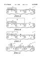
- FIGS. 1-8 illustrate, in cross-section, process steps in accordance with one embodiment of the invention.
- FIGS. 9-16 illustrate, in cross-section, process steps in accordance with an alternative embodiment of the invention.
- FIGS. 1-8 illustrate, in cross-section, a method for forming an integrated circuit in accordance with one embodiment of the present invention.
- a semiconductor substrate 10 having a field isolation region 12 and active regions 14, 16, and 18 formed therein.
- semiconductor substrate 10 is a monocrystalline silicon substrate.
- semiconductor substrate 10 may also be a silicon-on-insulator substrate, a silicon-on-sapphire substrate, or the like.
- field isolation region 12 is a trench isolation region which has been formed using conventional etching and chemical-mechanical polishing techniques.
- field isolation region 12 may be a field oxide region formed using conventional field oxide formation techniques, such as local oxidation of silicon (LOCOS), poly-buffered LOCOS (PBL), polysilicon encapsulated local oxidation (PELOX), or the like.
- LOCOS local oxidation of silicon
- PBL poly-buffered LOCOS
- PELOX polysilicon encapsulated local oxidation
- a gate dielectric layer 20 is formed overlying active region 14, active region 16, and active region 18.
- gate dielectric layer 20 is formed by thermally oxidizing a portion of semiconductor substrate 10 to form a thermal oxide layer that overlies active region 14, active region 16, and active region 18. This thermal oxide layer is then annealed in an ambient comprising nitrous oxide (NO 2 ) to form a nitrided oxide layer having a thickness ranging from approximately 2 nanometers to approximately 10 nanometers. It should be appreciated that the thermal oxide layer could also be annealed in other nitriding ambients, such as ammonia (NH 3 ) or nitric oxide (NO), to form a nitrided oxide layer.
- NH 3 ammonia
- NO nitric oxide
- gate dielectric layer may be a layer of thermal silicon dioxide, a layer of silicon nitride, a layer of silicon oxynitride, a layer of chemically vapor deposited silicon dioxide, or a combination thereof.
- a conductive polysilicon layer is then deposited so that it overlies active regions 14, 16, and 18.
- the polysilicon layer is then patterned to leave a remaining portion 22 of the polysilicon layer overlying active region 14, as shown in FIG. 2. It should also be appreciated that remaining portion 22 may also be formed with another conductive layer, such as an amorphous silicon layer, a silicon-germanium layer, or the like.
- an oxidation resistant layer 24 is then formed overlying remaining portion 22, active region 16, and active region 18.
- oxidation resistant layer 24 is an ONO dielectric layer.
- a first oxide layer is formed by thermally oxidizing a portion of remaining portion 22 and then a layer of silicon nitride is chemically vapor deposited to overlie this first oxide layer, active region 16, and active region 18.
- a surface portion of the silicon nitride layer is then re-oxidized to form a second oxide layer overlying the silicon nitride layer.
- the second oxide layer may be formed using a layer of chemical vapor deposited silicon oxide.
- oxidation resistant layer 24 need not be formed as a composite layer.
- oxidation resistant layer 24 may be formed using a layer of silicon nitride or a layer of silicon oxynitride.
- an etch mask 26 is formed overlying semiconductor substrate 10, and then a portion of oxidation resistant layer 24 and a portion of gate dielectric layer 20 that overlie active region 16 are removed to expose a surface portion 28 of semiconductor substrate 10.
- Oxidation resistant layer 24 and gate dielectric layer 20 may be removed using conventional dry or wet etching techniques or a combination thereof.
- oxidation resistant layer 24 may be removed using a fluorinated plasma etch chemistry and gate dielectric layer 20 may be removed using hydrofluoric acid.
- gate dielectric layer 30 is then formed overlying active region 16.
- gate dielectric layer 30 is a layer of thermal silicon dioxide having a thickness ranging from approximately 5 nanometers to approximately 50 nanometers, and is formed by thermally oxidizing surface portion 28 of semiconductor substrate 10.
- gate dielectric layer 30 may be a nitrided oxide layer, a silicon nitride layer, a silicon oxynitride layer, a layer of chemically vapor deposited silicon dioxide, or the like. It is important to note that oxidation resistant layer 24 protects active region 14 and active region 18 when gate dielectric layer 30 is formed.
- oxidation resistant layer 24 prevents active region 18, remaining portion 22, and active region 14 from being oxidized or nitrided when gate dielectric layer 30 is formed. More importantly, oxidation resistant layer 24 also prevents portions of the field isolation region 12 from being etched when surface portion 28 is exposed, as shown in FIG. 4. In addition, oxidation resistant layer 24 also prevents portions of the field isolation region 12 from being etched when surface portion 28 is subsequently cleaned with a pre-gate clean that comprises hydrofluoric acid or with other ambients that would etch field isolation region 12.
- an etch mask 32 is formed overlying active region 14 and active region 16. A portion of oxidation resistant layer 24 and a portion of gate dielectric layer 20 that overlie active region 18 are then removed to expose a surface portion 34 of semiconductor substrate 10. As previously discussed, oxidation resistant layer 24 and underlying gate dielectric layer 20 may be removed using conventional dry or wet etching techniques or a combination thereof.
- gate dielectric layer 36 is then formed overlying active region 18.
- gate dielectric layer 36 is a layer of thermal silicon dioxide having a thickness ranging from approximately 2 nanometers to approximately 15 nanometers, and is formed by oxidizing exposed portion 34 of semiconductor substrate 10.
- gate dielectric layer 36 may be a nitrided oxide layer, a silicon oxynitride layer, a silicon nitride layer, a layer of chemically vapor deposited silicon dioxide, or the like.
- Oxidation resistant layer 24 protects remaining portion 22 and active region 14 while gate dielectric layer 36 is formed. More importantly, oxidation resistant layer 24 also prevents portions of the field isolation region 12 from being etched when surface portion 34 is exposed.
- oxidation resistant layer 24 also prevents portions of the field isolation region 12 from being etched when surface portion 34 is subsequently cleaned with a pre-gate clean that comprises hydrofluoric acid or with other ambients that would etch field isolation region 12. It should be appreciated that gate dielectric layer 30 is exposed while gate dielectric layer 36 is formed. Therefore, the thickness and/or composition of gate dielectric layer 30 may change when gate dielectric layer 36 is formed. A polysilicon layer 38 is then formed overlying active region 14, active region 16, and active region 18, as shown in FIG. 7.
- the polysilicon layer 38 is patterned to form a gate electrode 40 overlying active region 18, a gate electrode 42 overlying active region 16, and a control electrode 44 overlying active region 14.
- remaining portion 22 is also patterned to form a floating gate 46, which is self-aligned to control gate electrode 44, as shown in FIG. 8.
- control gate electrode 44, gate electrode 40, and gate electrode 42 may be formed with a single etch step or in separate etch steps.
- control gate electrode 44, gate electrode 40, and gate electrode 42 may also be formed using an amorphous silicon layer, or other conductive layer, such as a metal layer, a metal silicide layer, a metal nitride layer, or a combination thereof.
- Source/drain regions 48 are then formed within active region 14, active region 16, and active region 18.
- a floating gate device 50 is formed within active region 14
- a transistor 52 is formed within active region 16
- a transistor 54 is formed within active region 18.
- second gate dielectric layer 30 has a higher breakdown voltage than third gate dielectric layer 36 because second gate dielectric layer 30 is thicker than third gate dielectric layer 36. Therefore, transistor 52 can be characterized as high breakdown voltage transistor and transistor 54 can be characterized as a low breakdown voltage transistor.
- an integrated circuit having devices with multiple gate dielectric layers can be fabricated, and etching of the field isolation region (12) which causes recessing or thinning of the field isolation region (12) can be minimized.
- FIGS. 9-16 illustrate, in cross section, a method for forming an integrated circuit in accordance with an alternative embodiment of the present invention.
- Shown in FIG. 9 is a portion 59 of a semiconductor substrate 10 wherein a pad oxide layer 60 and an oxidation resistant layer 62 have been formed overlying the semiconductor substrate of FIG. 1.
- pad oxide layer 60 is formed by thermally oxidizing a portion of semiconductor substrate 10 to form a thermal oxide layer that overlies active region 14, active region 16, and active region 18.
- pad oxide layer 60 may be a layer of chemically vapor deposited silicon dioxide.
- oxidation resistant layer 62 is formed by depositing a layer of silicon nitride over pad oxide layer 60.
- oxidation resistant layer 62 may be a layer of silicon oxynitride.
- an etch mask 64 is formed overlying active region 16 and active region 18.
- a portion of oxidation resistant layer 62 and a portion of pad oxide layer 60 that overlie active region 14 are then removed to expose a surface portion 66 of semiconductor substrate 10.
- Oxidation resistant layer 62 and underlying pad oxide layer 60 may be removed using conventional dry or wet etching techniques or a combination thereof.
- a gate dielectric layer 68 is then formed overlying active region 14.
- gate dielectric layer 68 is formed by thermally oxidizing a portion of semiconductor substrate 10 to form a thermal oxide layer that overlies active region 14. This thermal oxide layer is then annealed in an ambient comprising nitrous oxide (NO 2 ) to form a nitrided oxide layer having a thickness ranging from approximately 2 nanometers to approximately 10 nanometers. It should be appreciated that the thermal oxide layer could also be annealed in other nitriding ambients, such as ammonia (NH 3 ) or nitric oxide (NO), to form a nitrided oxide layer.
- NH 3 ammonia
- NO nitric oxide
- gate dielectric layer 68 may be a layer of thermal silicon dioxide, a layer of silicon nitride, a layer of silicon oxynitride, a layer of chemically vapor deposited silicon dioxide, or a combination thereof.
- oxidation resistant layer 62 protects active region 16 and active region 18 when gate dielectric layer 68 is formed. Specifically, oxidation resistant layer 62 prevents active region 16 and active region 18 from being oxidized or nitrided when gate dielectric layer 68 is formed. More importantly, oxidation resistant layer 62 also prevents portions of the field isolation region 12 from being etched when surface portion 66 is exposed. In addition, oxidation resistant layer 62 also prevents portions of the field isolation region 12 from being etched when surface portion 66 is subsequently cleaned with a pre-gate clean that comprises hydrofluoric acid or with other ambients that would etch field isolation region 12.
- a polysilicon layer is then formed overlying active region 14, active region 16 and active region 18. It is then patterned to leave a remaining portion 70 overlying active region 14. It should also be appreciated that remaining portion 70 may also be formed with another conductive layer, such as an amorphous silicon layer, a silicon-germanium layer, or the like.
- oxidation resistant layer 72 is then formed overlying remaining portion 70, active region 16, and active region 18.
- oxidation resistant layer 72 is an ONO dielectric layer.
- a first oxide layer is formed by thermally oxidizing a portion of remaining portion 70 and then a layer of silicon nitride is chemically vapor deposited to overly this first oxide layer, active region 16, and active region 18.
- a surface portion of the silicon nitride layer is then re-oxidized to form a second oxide layer overlying the silicon nitride layer.
- the second oxide layer may be formed using a layer of chemical vapor deposited silicon oxide. It should be appreciated that oxidation resistant layer 72 need not be formed as a composite layer.
- oxidation resistant layer 72 may be formed using a layer of silicon nitride or a layer of silicon oxynitride.
- oxidation resistant layer 62 which is overlying active region 16 and active region 18 in FIG. 11, may be removed prior to forming oxidation resistant layer 72.
- an etch mask 74 is then formed overlying active region 14, and active region 18.
- a portion of oxidation resistant layer 72, a portion of oxidation resistant layer 62, and a portion of pad oxide layer 60 that overly active region 16 are then removed to expose a surface portion 76 of semiconductor substrate 10.
- Oxidation resistant layer 72, oxidation resistant layer 62, and pad oxide layer 60 may be removed using conventional dry or wet etching techniques or a combination thereof.
- oxidation resistant layer 72 and oxidation resistant layer 62 may be removed using a fluorinated plasma etch chemistry, and pad oxide layer 60 may be removed using hydrofluoric acid.
- gate dielectric layer 78 is then formed overlying active region 16.
- gate dielectric layer 78 is a layer of thermal silicon dioxide having a thickness ranging from approximately 5 nanometers to approximately 50 nanometers, and is formed by thermally oxidizing surface portion 76 of semiconductor substrate 10.
- gate dielectric layer 78 may be a nitrided oxide layer, a silicon oxynitride layer, a layer of chemically vapor deposited silicon dioxide, or the like. It is important to note that oxidation resistant layer 62 and oxidation resistant layer 72 protect active region 14 and active region 18 when gate dielectric layer 78 is formed.
- oxidation resistant layer 62 and oxidation resistant layer 72 prevent active region 18, remaining portion 22, and active region 14 from being oxidized or nitrided when gate dielectric layer 78 is formed. More importantly, oxidation resistant layer 62 and oxidation resistant layer 72 also prevent portions of the field isolation region 12 from being etched when surface portion 76 is exposed. In addition, oxidation resistant layer 62 and oxidation resistant layer 72 also prevent portions of the field isolation region 12 from being etched when surface portion 76 is subsequently cleaned with a pre-gate clean that comprises hydrofluoric acid or with other ambients that would etch field isolation region 12.
- oxidation resistant layer 72 would prevent active region 18, remaining portion 22, and active region 14 from being oxidized or nitrided, and would also prevent portions of field isolation region 12 from being etched.
- an etch mask 80 is then formed overlying active region 14 and active region 16.
- a portion of oxidation resistant layer 72, oxidation a portion of resistant layer 62, and a portion of pad oxide layer 60 that overlie active region 18 are then removed to expose a surface portion 82 of semiconductor substrate 10.
- oxidation resistant layer 72, oxidation resistant layer 62, and pad oxide layer 60 may be removed using conventional dry or etching techniques or a combination thereof. Note, if oxidation resistant layer 62 is removed prior to forming oxidation resistant layer 72, as previously discussed, then a portion of oxidation resistant layer 72 and a portion of pad oxide layer 60 would be removed to expose a surface portion of semiconductor substrate 10.
- gate dielectric layer 84 is then formed overlying active region 18.
- gate dielectric layer 84 is a layer of thermal silicon dioxide having a thickness ranging from approximately 2 nanometers to approximately 15 nanometers, and is formed by thermally oxidizing surface portion 82 of semiconductor substrate 10.
- gate dielectric layer 84 may be a nitrided oxide layer, a silicon oxynitride layer, a silicon nitride layer, a layer of chemically vapor deposited silicon dioxide, or the like.
- oxidation resistant layer 72 protects remaining portion 70 and active region 14 while gate dielectric layer 84 is formed.
- oxidation resistant layer 72 also prevents portions of the field isolation region 12 from being etched when surface portion 82 is exposed. In addition, oxidation resistant layer 72 also prevents portions of the field isolation region 12 from being etched when surface portion 82 is subsequently cleaned with a pre-gate clean that comprises hydrofluoric acid. It should be appreciated that gate dielectric layer 78 is exposed while gate dielectric layer 84 is formed. Therefore, the thickness and/or composition of gate dielectric layer 78 may change when gate dielectric layer 84 is formed.
- a polysilicon layer is then formed overlying remaining portion 70, active region 16, and active region 18. It is then patterned to form a gate electrode 86 overlying active region 18, a gate electrode 88 overlying active region 16, and a control gate electrode 90 overlying active region 14. In one embodiment, remaining portion 70 is also patterned to form a floating gate 92 which is self-aligned to control gate electrode 90, as shown in FIG. 16. It should be appreciated that control gate electrode 90, gate electrode 88, and gate electrode 86 may be formed with a single etch step or in separate etch steps.
- control gate electrode 90, gate electrode 88, and gate electrode 86 may also be formed using an amorphous silicon layer, or other conductive layer, such as a metal layer, a metal silicide layer, a metal nitride layer, or a combination thereof.
- Source/drain regions 94 are then formed within active region 14, active region 16, and active region 18.
- a floating gate device 96 is formed within active region 14
- a transistor 98 is formed within active region 16
- a transistor 100 is formed within active region 18.
- second gate dielectric layer 78 has a higher breakdown voltage than third gate dielectric layer 84 because second gate dielectric layer 78 is thicker than third gate dielectric layer 84. Therefore, transistor 98 can be characterized as high breakdown voltage transistor and transistor 100 can be characterized as a low breakdown voltage transistor.
- an integrated circuit having devices with multiple gate dielectric layers can be fabricated, and etching of the field isolation region (12) which causes recessing or thinning of the field isolation region (12) can be minimized.
Abstract
Description
Claims (13)
Priority Applications (1)
| Application Number | Priority Date | Filing Date | Title |
|---|---|---|---|
| US09/015,957 US6133093A (en) | 1998-01-30 | 1998-01-30 | Method for forming an integrated circuit |
Applications Claiming Priority (1)
| Application Number | Priority Date | Filing Date | Title |
|---|---|---|---|
| US09/015,957 US6133093A (en) | 1998-01-30 | 1998-01-30 | Method for forming an integrated circuit |
Publications (1)
| Publication Number | Publication Date |
|---|---|
| US6133093A true US6133093A (en) | 2000-10-17 |
Family
ID=21774547
Family Applications (1)
| Application Number | Title | Priority Date | Filing Date |
|---|---|---|---|
| US09/015,957 Expired - Lifetime US6133093A (en) | 1998-01-30 | 1998-01-30 | Method for forming an integrated circuit |
Country Status (1)
| Country | Link |
|---|---|
| US (1) | US6133093A (en) |
Cited By (26)
| Publication number | Priority date | Publication date | Assignee | Title |
|---|---|---|---|---|
| US6265267B1 (en) * | 1999-11-04 | 2001-07-24 | United Microelectronics Corp. | Fabricating method for a semiconductor device comprising gate oxide layers of various thicknesses |
| US6306690B1 (en) * | 1997-10-30 | 2001-10-23 | Texas Instruments Incorporated | Process flow to integrate high and low voltage peripheral transistors with a floating gate array |
| US6344394B1 (en) * | 1999-06-03 | 2002-02-05 | Mitsubishi Denki Kabushiki Kaisha | Method of manufacturing a semiconductor memory device having a capacitor with improved dielectric layer |
| US6444555B2 (en) * | 1999-12-07 | 2002-09-03 | Advanced Micro Devices, Inc. | Method for establishing ultra-thin gate insulator using anneal in ammonia |
| US20030080354A1 (en) * | 2001-10-18 | 2003-05-01 | Seiko Epson Corporation | Method for manufacturing semiconductor device, and semiconductor device |
| US6559012B2 (en) * | 1997-12-09 | 2003-05-06 | Hitachi, Ltd. | Method for manufacturing semiconductor integrated circuit device having floating gate and deposited film |
| US20030156380A1 (en) * | 1993-04-02 | 2003-08-21 | Micron Technology, Inc. | Capacitor compatible with high dielectric constant materials having two independent insulative layers and the method for forming same |
| US6624468B2 (en) * | 1999-03-12 | 2003-09-23 | Kabushiki Kaisha Toshiba | Semiconductor device including insulated gate field effect transistors |
| US6690030B2 (en) * | 2000-03-06 | 2004-02-10 | Kabushiki Kaisha Toshiba | Semiconductor device with negative differential resistance characteristics |
| US20040126949A1 (en) * | 2002-08-19 | 2004-07-01 | Samsung Electronics Co., Ltd. | Gate electrode of a semiconductor device and method of forming the same |
| US6787840B1 (en) * | 2000-01-27 | 2004-09-07 | Advanced Micro Devices, Inc. | Nitridated tunnel oxide barriers for flash memory technology circuitry |
| US6835622B2 (en) * | 2002-06-04 | 2004-12-28 | Taiwan Semiconductor Manufacturing Co., Ltd | Gate electrode doping method for forming semiconductor integrated circuit microelectronic fabrication with varying effective gate dielectric layer thicknesses |
| US20050067663A1 (en) * | 2003-09-26 | 2005-03-31 | Krishnaswamy Ramkumar | Oxide-nitride stack gate dielectric |
| US20050085042A1 (en) * | 2003-06-23 | 2005-04-21 | Jong-Sik Chun | Dual gate oxide structure in semiconductor device and method thereof |
| US20050114722A1 (en) * | 2003-11-25 | 2005-05-26 | Matsushita Electric Industrial Co., Ltd. | Semiconductor integrated circuit and microprocessor unit switching method |
| US20050207226A1 (en) * | 2002-10-09 | 2005-09-22 | Yuan Jack H | Flash memory array with increased coupling between floating and control gates |
| US20060134864A1 (en) * | 2004-12-22 | 2006-06-22 | Masaaki Higashitani | Multi-thickness dielectric for semiconductor memory |
| US20060211200A1 (en) * | 2005-03-15 | 2006-09-21 | Oki Electric Industry Co., Ltd. | Method of manufacturing semiconductor device |
| US7241700B1 (en) | 2004-10-20 | 2007-07-10 | Advanced Micro Devices, Inc. | Methods for post offset spacer clean for improved selective epitaxy silicon growth |
| US7402207B1 (en) | 2004-05-05 | 2008-07-22 | Advanced Micro Devices, Inc. | Method and apparatus for controlling the thickness of a selective epitaxial growth layer |
| US7402485B1 (en) | 2004-10-20 | 2008-07-22 | Advanced Micro Devices, Inc. | Method of forming a semiconductor device |
| US7456062B1 (en) | 2004-10-20 | 2008-11-25 | Advanced Micro Devices, Inc. | Method of forming a semiconductor device |
| US7553732B1 (en) | 2005-06-13 | 2009-06-30 | Advanced Micro Devices, Inc. | Integration scheme for constrained SEG growth on poly during raised S/D processing |
| US7572705B1 (en) | 2005-09-21 | 2009-08-11 | Advanced Micro Devices, Inc. | Semiconductor device and method of manufacturing a semiconductor device |
| US20110195558A1 (en) * | 2002-07-09 | 2011-08-11 | Eiji Kamiya | Non-volatile semiconductor memory device and method of manufacturing the same |
| US20190043878A1 (en) * | 2015-12-29 | 2019-02-07 | Taiwan Semiconductor Manufacturing Co., Ltd. | Method to fabricate uniform tunneling dielectric of embedded flash memory cell |
Citations (6)
| Publication number | Priority date | Publication date | Assignee | Title |
|---|---|---|---|---|
| US4420871A (en) * | 1980-10-06 | 1983-12-20 | Siemens Aktiengesellschaft | Method of producing a monolithically integrated two-transistor memory cell in accordance with MOS technology |
| US5116775A (en) * | 1986-06-18 | 1992-05-26 | Hitachi, Ltd. | Method of producing semiconductor memory device with buried barrier layer |
| US5278087A (en) * | 1990-01-22 | 1994-01-11 | Silicon Storage Technology, Inc. | Method of making a single transistor non-volatile electrically alterable semiconductor memory device with a re-crystallized floating gate |
| US5587332A (en) * | 1992-09-01 | 1996-12-24 | Vlsi Technology, Inc. | Method of making flash memory cell |
| US5830795A (en) * | 1996-06-10 | 1998-11-03 | Advanced Micro Devices, Inc. | Simplified masking process for programmable logic device manufacture |
| US5861347A (en) * | 1997-07-03 | 1999-01-19 | Motorola Inc. | Method for forming a high voltage gate dielectric for use in integrated circuit |
-
1998
- 1998-01-30 US US09/015,957 patent/US6133093A/en not_active Expired - Lifetime
Patent Citations (6)
| Publication number | Priority date | Publication date | Assignee | Title |
|---|---|---|---|---|
| US4420871A (en) * | 1980-10-06 | 1983-12-20 | Siemens Aktiengesellschaft | Method of producing a monolithically integrated two-transistor memory cell in accordance with MOS technology |
| US5116775A (en) * | 1986-06-18 | 1992-05-26 | Hitachi, Ltd. | Method of producing semiconductor memory device with buried barrier layer |
| US5278087A (en) * | 1990-01-22 | 1994-01-11 | Silicon Storage Technology, Inc. | Method of making a single transistor non-volatile electrically alterable semiconductor memory device with a re-crystallized floating gate |
| US5587332A (en) * | 1992-09-01 | 1996-12-24 | Vlsi Technology, Inc. | Method of making flash memory cell |
| US5830795A (en) * | 1996-06-10 | 1998-11-03 | Advanced Micro Devices, Inc. | Simplified masking process for programmable logic device manufacture |
| US5861347A (en) * | 1997-07-03 | 1999-01-19 | Motorola Inc. | Method for forming a high voltage gate dielectric for use in integrated circuit |
Cited By (47)
| Publication number | Priority date | Publication date | Assignee | Title |
|---|---|---|---|---|
| US6762924B2 (en) * | 1993-04-02 | 2004-07-13 | Micron Technology, Inc. | Capacitor compatible with high dielectric constant materials having two independent insulative layers and the method for forming same |
| US20030156380A1 (en) * | 1993-04-02 | 2003-08-21 | Micron Technology, Inc. | Capacitor compatible with high dielectric constant materials having two independent insulative layers and the method for forming same |
| US6306690B1 (en) * | 1997-10-30 | 2001-10-23 | Texas Instruments Incorporated | Process flow to integrate high and low voltage peripheral transistors with a floating gate array |
| US6559012B2 (en) * | 1997-12-09 | 2003-05-06 | Hitachi, Ltd. | Method for manufacturing semiconductor integrated circuit device having floating gate and deposited film |
| US6624468B2 (en) * | 1999-03-12 | 2003-09-23 | Kabushiki Kaisha Toshiba | Semiconductor device including insulated gate field effect transistors |
| US6448189B1 (en) | 1999-06-03 | 2002-09-10 | Mitsubishi Denki Kabushiki Kaisha | Method of manufacturing a semiconductor memory device having a capacitor with improved dielectric layer |
| US6605503B2 (en) | 1999-06-03 | 2003-08-12 | Mitsubishi Denki Kabushiki Kaisha | Method of manufacturing a semiconductor memory device having a capacitor with improved dielectric layer |
| US6344394B1 (en) * | 1999-06-03 | 2002-02-05 | Mitsubishi Denki Kabushiki Kaisha | Method of manufacturing a semiconductor memory device having a capacitor with improved dielectric layer |
| US6265267B1 (en) * | 1999-11-04 | 2001-07-24 | United Microelectronics Corp. | Fabricating method for a semiconductor device comprising gate oxide layers of various thicknesses |
| US6444555B2 (en) * | 1999-12-07 | 2002-09-03 | Advanced Micro Devices, Inc. | Method for establishing ultra-thin gate insulator using anneal in ammonia |
| US6787840B1 (en) * | 2000-01-27 | 2004-09-07 | Advanced Micro Devices, Inc. | Nitridated tunnel oxide barriers for flash memory technology circuitry |
| US6690030B2 (en) * | 2000-03-06 | 2004-02-10 | Kabushiki Kaisha Toshiba | Semiconductor device with negative differential resistance characteristics |
| US20030080354A1 (en) * | 2001-10-18 | 2003-05-01 | Seiko Epson Corporation | Method for manufacturing semiconductor device, and semiconductor device |
| US6835622B2 (en) * | 2002-06-04 | 2004-12-28 | Taiwan Semiconductor Manufacturing Co., Ltd | Gate electrode doping method for forming semiconductor integrated circuit microelectronic fabrication with varying effective gate dielectric layer thicknesses |
| US8674431B2 (en) | 2002-07-09 | 2014-03-18 | Kabushiki Kaisha Toshiba | Non-volatile semiconductor memory device and method of manufacturing the same |
| US8138043B2 (en) * | 2002-07-09 | 2012-03-20 | Kabushiki Kaisha Toshiba | Non-volatile semiconductor memory device and method of manufacturing the same |
| US20110195558A1 (en) * | 2002-07-09 | 2011-08-11 | Eiji Kamiya | Non-volatile semiconductor memory device and method of manufacturing the same |
| US7074671B2 (en) * | 2002-08-19 | 2006-07-11 | Samsung Electronics Co., Ltd. | Gate electrode of a semiconductor device and method of forming the same |
| US20040126949A1 (en) * | 2002-08-19 | 2004-07-01 | Samsung Electronics Co., Ltd. | Gate electrode of a semiconductor device and method of forming the same |
| US7170131B2 (en) | 2002-10-09 | 2007-01-30 | Sandisk Corporation | Flash memory array with increased coupling between floating and control gates |
| US7517756B2 (en) | 2002-10-09 | 2009-04-14 | Sandisk Corporation | Flash memory array with increased coupling between floating and control gates |
| US20050207226A1 (en) * | 2002-10-09 | 2005-09-22 | Yuan Jack H | Flash memory array with increased coupling between floating and control gates |
| US20070122980A1 (en) * | 2002-10-09 | 2007-05-31 | Yuan Jack H | Flash Memory Array with Increased Coupling Between Floating and Control Gates |
| US7250346B2 (en) | 2003-06-23 | 2007-07-31 | Samsung Electronics Col., Ltd. | Dual gate oxide structure in semiconductor device and method thereof |
| US20070246779A1 (en) * | 2003-06-23 | 2007-10-25 | Samsung Electronics Co., Ltd. | Dual gate oxide structure in semiconductor device and method thereof |
| US20050085042A1 (en) * | 2003-06-23 | 2005-04-21 | Jong-Sik Chun | Dual gate oxide structure in semiconductor device and method thereof |
| US20050067663A1 (en) * | 2003-09-26 | 2005-03-31 | Krishnaswamy Ramkumar | Oxide-nitride stack gate dielectric |
| US8445381B2 (en) | 2003-09-26 | 2013-05-21 | Cypress Semiconductor Corporation | Oxide-nitride stack gate dielectric |
| US20080093680A1 (en) * | 2003-09-26 | 2008-04-24 | Krishnaswamy Ramkumar | Oxide-nitride stack gate dielectric |
| US7371637B2 (en) * | 2003-09-26 | 2008-05-13 | Cypress Semiconductor Corporation | Oxide-nitride stack gate dielectric |
| US20050114722A1 (en) * | 2003-11-25 | 2005-05-26 | Matsushita Electric Industrial Co., Ltd. | Semiconductor integrated circuit and microprocessor unit switching method |
| US7402207B1 (en) | 2004-05-05 | 2008-07-22 | Advanced Micro Devices, Inc. | Method and apparatus for controlling the thickness of a selective epitaxial growth layer |
| US7456062B1 (en) | 2004-10-20 | 2008-11-25 | Advanced Micro Devices, Inc. | Method of forming a semiconductor device |
| US7402485B1 (en) | 2004-10-20 | 2008-07-22 | Advanced Micro Devices, Inc. | Method of forming a semiconductor device |
| US7241700B1 (en) | 2004-10-20 | 2007-07-10 | Advanced Micro Devices, Inc. | Methods for post offset spacer clean for improved selective epitaxy silicon growth |
| US20060134864A1 (en) * | 2004-12-22 | 2006-06-22 | Masaaki Higashitani | Multi-thickness dielectric for semiconductor memory |
| US7482223B2 (en) * | 2004-12-22 | 2009-01-27 | Sandisk Corporation | Multi-thickness dielectric for semiconductor memory |
| US20060211200A1 (en) * | 2005-03-15 | 2006-09-21 | Oki Electric Industry Co., Ltd. | Method of manufacturing semiconductor device |
| US7291534B2 (en) * | 2005-03-15 | 2007-11-06 | Oki Electric Industry Co., Ltd. | Method of manufacturing semiconductor device |
| US7553732B1 (en) | 2005-06-13 | 2009-06-30 | Advanced Micro Devices, Inc. | Integration scheme for constrained SEG growth on poly during raised S/D processing |
| US7910996B2 (en) | 2005-09-21 | 2011-03-22 | Globalfoundries Inc. | Semiconductor device and method of manufacturing a semiconductor device |
| US20090267152A1 (en) * | 2005-09-21 | 2009-10-29 | Advanced Micro Devices, Inc. | Semiconductor device and method of manufacturing a semiconductor device |
| US7572705B1 (en) | 2005-09-21 | 2009-08-11 | Advanced Micro Devices, Inc. | Semiconductor device and method of manufacturing a semiconductor device |
| US20190043878A1 (en) * | 2015-12-29 | 2019-02-07 | Taiwan Semiconductor Manufacturing Co., Ltd. | Method to fabricate uniform tunneling dielectric of embedded flash memory cell |
| US10879257B2 (en) * | 2015-12-29 | 2020-12-29 | Taiwan Semiconductor Manufacturing Co., Ltd. | Integrated chip having a logic gate electrode and a tunnel dielectric layer |
| US11532637B2 (en) | 2015-12-29 | 2022-12-20 | Taiwan Semiconductor Manufacturing Company, Ltd. | Embedded flash memory cell including a tunnel dielectric layer having different thicknesses over a memory region |
| US20230109273A1 (en) * | 2015-12-29 | 2023-04-06 | Taiwan Semiconductor Manufacturing Company, Ltd. | Method to fabricate uniform tunneling dielectric of embedded flash memory cell |
Similar Documents
| Publication | Publication Date | Title |
|---|---|---|
| US6133093A (en) | Method for forming an integrated circuit | |
| US6890811B2 (en) | Dual gate dielectric scheme: SiON for high performance devices and high k for low power devices | |
| EP0646956B1 (en) | Method of formation of a trench isolation structure in an integrated circuit | |
| US5786263A (en) | Method for forming a trench isolation structure in an integrated circuit | |
| US6524931B1 (en) | Method for forming a trench isolation structure in an integrated circuit | |
| US6054343A (en) | Nitride trench fill process for increasing shallow trench isolation (STI) robustness | |
| US20040198000A1 (en) | Method of generating multiple oxides by plasma nitridation on oxide | |
| US6130168A (en) | Using ONO as hard mask to reduce STI oxide loss on low voltage device in flash or EPROM process | |
| US7804146B2 (en) | Semiconductor device and method for fabricating the same | |
| US5966606A (en) | Method for manufacturing a MOSFET having a side-wall film formed through nitridation of the gate electrode | |
| US7160771B2 (en) | Forming gate oxides having multiple thicknesses | |
| US20030003644A1 (en) | Semiconductor integrated circuit device and method of fabricating the same | |
| CN100334732C (en) | Semiconductor integrated circuit device and its mfg. method | |
| US7638396B2 (en) | Methods for fabricating a semiconductor device | |
| US8617954B2 (en) | Formation of nitrogen containing dielectric layers having an improved nitrogen distribution | |
| US6734114B2 (en) | Method for manufacturing semiconductor integrated circuit device | |
| US20050059215A1 (en) | Semiconductor device with dual gate oxides | |
| US6511887B1 (en) | Method for making FET gate oxides with different thicknesses using a thin silicon nitride layer and a single oxidation step | |
| US20050085048A1 (en) | Method of fabricating shallow trench isolation with improved smiling effect | |
| US5985725A (en) | Method for manufacturing dual gate oxide layer | |
| US7316979B2 (en) | Method and apparatus for providing an integrated active region on silicon-on-insulator devices | |
| US6833330B1 (en) | Method to eliminate inverse narrow width effect in small geometry MOS transistors | |
| JP2008021935A (en) | Electronic device and manufacturing method thereof | |
| KR100839894B1 (en) | Semiconductor device and fabrication method therefor | |
| US7524720B2 (en) | Method of manufacturing semiconductor device |
Legal Events
| Date | Code | Title | Description |
|---|---|---|---|
| AS | Assignment |
Owner name: MOTOROLA, INC., ILLINOIS Free format text: ASSIGNMENT OF ASSIGNORS INTEREST;ASSIGNORS:PRINZ, ERWIN J.;WU, KEVIN YUN-KANG;BAKER, FRANK KELSEY;REEL/FRAME:008951/0427 Effective date: 19980126 |
|
| AS | Assignment |
Owner name: MOTOROLA, INC., ILLINOIS Free format text: ASSIGNMENT OF ASSIGNORS INTEREST;ASSIGNORS:YERIC, GREGORY M.;CHEN, WEI-MING;REEL/FRAME:010151/0338;SIGNING DATES FROM 19980318 TO 19980914 |
|
| STCF | Information on status: patent grant |
Free format text: PATENTED CASE |
|
| CC | Certificate of correction | ||
| FPAY | Fee payment |
Year of fee payment: 4 |
|
| AS | Assignment |
Owner name: FREESCALE SEMICONDUCTOR, INC., TEXAS Free format text: ASSIGNMENT OF ASSIGNORS INTEREST;ASSIGNOR:MOTOROLA, INC.;REEL/FRAME:015698/0657 Effective date: 20040404 Owner name: FREESCALE SEMICONDUCTOR, INC.,TEXAS Free format text: ASSIGNMENT OF ASSIGNORS INTEREST;ASSIGNOR:MOTOROLA, INC.;REEL/FRAME:015698/0657 Effective date: 20040404 |
|
| AS | Assignment |
Owner name: CITIBANK, N.A. AS COLLATERAL AGENT, NEW YORK Free format text: SECURITY AGREEMENT;ASSIGNORS:FREESCALE SEMICONDUCTOR, INC.;FREESCALE ACQUISITION CORPORATION;FREESCALE ACQUISITION HOLDINGS CORP.;AND OTHERS;REEL/FRAME:018855/0129 Effective date: 20061201 Owner name: CITIBANK, N.A. AS COLLATERAL AGENT,NEW YORK Free format text: SECURITY AGREEMENT;ASSIGNORS:FREESCALE SEMICONDUCTOR, INC.;FREESCALE ACQUISITION CORPORATION;FREESCALE ACQUISITION HOLDINGS CORP.;AND OTHERS;REEL/FRAME:018855/0129 Effective date: 20061201 |
|
| FPAY | Fee payment |
Year of fee payment: 8 |
|
| AS | Assignment |
Owner name: CITIBANK, N.A., AS COLLATERAL AGENT,NEW YORK Free format text: SECURITY AGREEMENT;ASSIGNOR:FREESCALE SEMICONDUCTOR, INC.;REEL/FRAME:024397/0001 Effective date: 20100413 Owner name: CITIBANK, N.A., AS COLLATERAL AGENT, NEW YORK Free format text: SECURITY AGREEMENT;ASSIGNOR:FREESCALE SEMICONDUCTOR, INC.;REEL/FRAME:024397/0001 Effective date: 20100413 |
|
| FPAY | Fee payment |
Year of fee payment: 12 |
|
| AS | Assignment |
Owner name: CITIBANK, N.A., AS NOTES COLLATERAL AGENT, NEW YOR Free format text: SECURITY AGREEMENT;ASSIGNOR:FREESCALE SEMICONDUCTOR, INC.;REEL/FRAME:030633/0424 Effective date: 20130521 |
|
| AS | Assignment |
Owner name: CITIBANK, N.A., AS NOTES COLLATERAL AGENT, NEW YOR Free format text: SECURITY AGREEMENT;ASSIGNOR:FREESCALE SEMICONDUCTOR, INC.;REEL/FRAME:031591/0266 Effective date: 20131101 |
|
| AS | Assignment |
Owner name: FREESCALE SEMICONDUCTOR, INC., TEXAS Free format text: PATENT RELEASE;ASSIGNOR:CITIBANK, N.A., AS COLLATERAL AGENT;REEL/FRAME:037356/0553 Effective date: 20151207 Owner name: FREESCALE SEMICONDUCTOR, INC., TEXAS Free format text: PATENT RELEASE;ASSIGNOR:CITIBANK, N.A., AS COLLATERAL AGENT;REEL/FRAME:037354/0225 Effective date: 20151207 Owner name: FREESCALE SEMICONDUCTOR, INC., TEXAS Free format text: PATENT RELEASE;ASSIGNOR:CITIBANK, N.A., AS COLLATERAL AGENT;REEL/FRAME:037356/0143 Effective date: 20151207 |
|
| AS | Assignment |
Owner name: MORGAN STANLEY SENIOR FUNDING, INC., MARYLAND Free format text: ASSIGNMENT AND ASSUMPTION OF SECURITY INTEREST IN PATENTS;ASSIGNOR:CITIBANK, N.A.;REEL/FRAME:037486/0517 Effective date: 20151207 |
|
| AS | Assignment |
Owner name: MORGAN STANLEY SENIOR FUNDING, INC., MARYLAND Free format text: ASSIGNMENT AND ASSUMPTION OF SECURITY INTEREST IN PATENTS;ASSIGNOR:CITIBANK, N.A.;REEL/FRAME:037518/0292 Effective date: 20151207 |
|
| AS | Assignment |
Owner name: MORGAN STANLEY SENIOR FUNDING, INC., MARYLAND Free format text: SUPPLEMENT TO THE SECURITY AGREEMENT;ASSIGNOR:FREESCALE SEMICONDUCTOR, INC.;REEL/FRAME:039138/0001 Effective date: 20160525 |
|
| AS | Assignment |
Owner name: NXP, B.V., F/K/A FREESCALE SEMICONDUCTOR, INC., NETHERLANDS Free format text: RELEASE BY SECURED PARTY;ASSIGNOR:MORGAN STANLEY SENIOR FUNDING, INC.;REEL/FRAME:040925/0001 Effective date: 20160912 Owner name: NXP, B.V., F/K/A FREESCALE SEMICONDUCTOR, INC., NE Free format text: RELEASE BY SECURED PARTY;ASSIGNOR:MORGAN STANLEY SENIOR FUNDING, INC.;REEL/FRAME:040925/0001 Effective date: 20160912 |
|
| AS | Assignment |
Owner name: NXP B.V., NETHERLANDS Free format text: RELEASE BY SECURED PARTY;ASSIGNOR:MORGAN STANLEY SENIOR FUNDING, INC.;REEL/FRAME:040928/0001 Effective date: 20160622 |
|
| AS | Assignment |
Owner name: NXP USA, INC., TEXAS Free format text: CHANGE OF NAME;ASSIGNOR:FREESCALE SEMICONDUCTOR INC.;REEL/FRAME:040652/0180 Effective date: 20161107 |
|
| AS | Assignment |
Owner name: NXP USA, INC., TEXAS Free format text: CORRECTIVE ASSIGNMENT TO CORRECT THE NATURE OF CONVEYANCE LISTED CHANGE OF NAME SHOULD BE MERGER AND CHANGE PREVIOUSLY RECORDED AT REEL: 040652 FRAME: 0180. ASSIGNOR(S) HEREBY CONFIRMS THE MERGER AND CHANGE OF NAME;ASSIGNOR:FREESCALE SEMICONDUCTOR INC.;REEL/FRAME:041354/0148 Effective date: 20161107 |
|
| AS | Assignment |
Owner name: MORGAN STANLEY SENIOR FUNDING, INC., MARYLAND Free format text: CORRECTIVE ASSIGNMENT TO CORRECT THE REMOVE PATENTS 8108266 AND 8062324 AND REPLACE THEM WITH 6108266 AND 8060324 PREVIOUSLY RECORDED ON REEL 037518 FRAME 0292. ASSIGNOR(S) HEREBY CONFIRMS THE ASSIGNMENT AND ASSUMPTION OF SECURITY INTEREST IN PATENTS;ASSIGNOR:CITIBANK, N.A.;REEL/FRAME:041703/0536 Effective date: 20151207 |
|
| AS | Assignment |
Owner name: SHENZHEN XINGUODU TECHNOLOGY CO., LTD., CHINA Free format text: CORRECTIVE ASSIGNMENT TO CORRECT THE TO CORRECT THE APPLICATION NO. FROM 13,883,290 TO 13,833,290 PREVIOUSLY RECORDED ON REEL 041703 FRAME 0536. ASSIGNOR(S) HEREBY CONFIRMS THE THE ASSIGNMENT AND ASSUMPTION OF SECURITYINTEREST IN PATENTS.;ASSIGNOR:MORGAN STANLEY SENIOR FUNDING, INC.;REEL/FRAME:048734/0001 Effective date: 20190217 |
|
| AS | Assignment |
Owner name: NXP B.V., NETHERLANDS Free format text: RELEASE BY SECURED PARTY;ASSIGNOR:MORGAN STANLEY SENIOR FUNDING, INC.;REEL/FRAME:050744/0097 Effective date: 20190903 |
|
| AS | Assignment |
Owner name: MORGAN STANLEY SENIOR FUNDING, INC., MARYLAND Free format text: CORRECTIVE ASSIGNMENT TO CORRECT THE REMOVE APPLICATION11759915 AND REPLACE IT WITH APPLICATION 11759935 PREVIOUSLY RECORDED ON REEL 037486 FRAME 0517. ASSIGNOR(S) HEREBY CONFIRMS THE ASSIGNMENT AND ASSUMPTION OF SECURITYINTEREST IN PATENTS;ASSIGNOR:CITIBANK, N.A.;REEL/FRAME:053547/0421 Effective date: 20151207 |
|
| AS | Assignment |
Owner name: NXP B.V., NETHERLANDS Free format text: CORRECTIVE ASSIGNMENT TO CORRECT THE REMOVEAPPLICATION 11759915 AND REPLACE IT WITH APPLICATION11759935 PREVIOUSLY RECORDED ON REEL 040928 FRAME 0001. ASSIGNOR(S) HEREBY CONFIRMS THE RELEASE OF SECURITYINTEREST;ASSIGNOR:MORGAN STANLEY SENIOR FUNDING, INC.;REEL/FRAME:052915/0001 Effective date: 20160622 |
|
| AS | Assignment |
Owner name: NXP, B.V. F/K/A FREESCALE SEMICONDUCTOR, INC., NETHERLANDS Free format text: CORRECTIVE ASSIGNMENT TO CORRECT THE REMOVEAPPLICATION 11759915 AND REPLACE IT WITH APPLICATION11759935 PREVIOUSLY RECORDED ON REEL 040925 FRAME 0001. ASSIGNOR(S) HEREBY CONFIRMS THE RELEASE OF SECURITYINTEREST;ASSIGNOR:MORGAN STANLEY SENIOR FUNDING, INC.;REEL/FRAME:052917/0001 Effective date: 20160912 |