US6147378A - Fully recessed semiconductor device and method for low power applications with single wrap around buried drain region - Google Patents
Fully recessed semiconductor device and method for low power applications with single wrap around buried drain region Download PDFInfo
- Publication number
- US6147378A US6147378A US09/052,060 US5206098A US6147378A US 6147378 A US6147378 A US 6147378A US 5206098 A US5206098 A US 5206098A US 6147378 A US6147378 A US 6147378A
- Authority
- US
- United States
- Prior art keywords
- trench
- region
- buried
- trenched
- substrate
- Prior art date
- Legal status (The legal status is an assumption and is not a legal conclusion. Google has not performed a legal analysis and makes no representation as to the accuracy of the status listed.)
- Expired - Fee Related
Links
- 239000004065 semiconductor Substances 0.000 title claims abstract description 79
- 238000000034 method Methods 0.000 title abstract description 18
- 239000000758 substrate Substances 0.000 claims abstract description 74
- 238000009792 diffusion process Methods 0.000 claims description 17
- 238000012876 topography Methods 0.000 abstract description 4
- 239000010410 layer Substances 0.000 description 82
- 229910021420 polycrystalline silicon Inorganic materials 0.000 description 21
- 229920005591 polysilicon Polymers 0.000 description 21
- 239000007943 implant Substances 0.000 description 11
- 239000012535 impurity Substances 0.000 description 10
- 150000004767 nitrides Chemical class 0.000 description 10
- 239000002019 doping agent Substances 0.000 description 9
- WQJQOUPTWCFRMM-UHFFFAOYSA-N tungsten disilicide Chemical compound [Si]#[W]#[Si] WQJQOUPTWCFRMM-UHFFFAOYSA-N 0.000 description 8
- 229910021342 tungsten silicide Inorganic materials 0.000 description 8
- XUIMIQQOPSSXEZ-UHFFFAOYSA-N Silicon Chemical compound [Si] XUIMIQQOPSSXEZ-UHFFFAOYSA-N 0.000 description 7
- 230000015572 biosynthetic process Effects 0.000 description 7
- 229910052710 silicon Inorganic materials 0.000 description 7
- 239000010703 silicon Substances 0.000 description 7
- 239000000463 material Substances 0.000 description 5
- 230000015654 memory Effects 0.000 description 5
- 125000006850 spacer group Chemical group 0.000 description 5
- ZOXJGFHDIHLPTG-UHFFFAOYSA-N Boron Chemical compound [B] ZOXJGFHDIHLPTG-UHFFFAOYSA-N 0.000 description 4
- 229910052796 boron Inorganic materials 0.000 description 4
- 238000000151 deposition Methods 0.000 description 4
- BHEPBYXIRTUNPN-UHFFFAOYSA-N hydridophosphorus(.) (triplet) Chemical compound [PH] BHEPBYXIRTUNPN-UHFFFAOYSA-N 0.000 description 4
- 239000011229 interlayer Substances 0.000 description 4
- 238000004519 manufacturing process Methods 0.000 description 4
- 229910052785 arsenic Inorganic materials 0.000 description 3
- RQNWIZPPADIBDY-UHFFFAOYSA-N arsenic atom Chemical compound [As] RQNWIZPPADIBDY-UHFFFAOYSA-N 0.000 description 3
- 238000005530 etching Methods 0.000 description 3
- 238000005468 ion implantation Methods 0.000 description 3
- 238000012856 packing Methods 0.000 description 3
- WFKWXMTUELFFGS-UHFFFAOYSA-N tungsten Chemical compound [W] WFKWXMTUELFFGS-UHFFFAOYSA-N 0.000 description 3
- 229910052721 tungsten Inorganic materials 0.000 description 3
- 239000010937 tungsten Substances 0.000 description 3
- BOTDANWDWHJENH-UHFFFAOYSA-N Tetraethyl orthosilicate Chemical compound CCO[Si](OCC)(OCC)OCC BOTDANWDWHJENH-UHFFFAOYSA-N 0.000 description 2
- 238000005229 chemical vapour deposition Methods 0.000 description 2
- 239000004020 conductor Substances 0.000 description 2
- 230000008878 coupling Effects 0.000 description 2
- 238000010168 coupling process Methods 0.000 description 2
- 238000005859 coupling reaction Methods 0.000 description 2
- 239000013078 crystal Substances 0.000 description 2
- 230000008021 deposition Effects 0.000 description 2
- 238000002347 injection Methods 0.000 description 2
- 239000007924 injection Substances 0.000 description 2
- 238000004518 low pressure chemical vapour deposition Methods 0.000 description 2
- 230000035945 sensitivity Effects 0.000 description 2
- 208000032750 Device leakage Diseases 0.000 description 1
- 230000005689 Fowler Nordheim tunneling Effects 0.000 description 1
- 229910007277 Si3 N4 Inorganic materials 0.000 description 1
- 229910052581 Si3N4 Inorganic materials 0.000 description 1
- 238000007796 conventional method Methods 0.000 description 1
- 239000003989 dielectric material Substances 0.000 description 1
- 230000000694 effects Effects 0.000 description 1
- 238000002513 implantation Methods 0.000 description 1
- 238000011065 in-situ storage Methods 0.000 description 1
- 238000002955 isolation Methods 0.000 description 1
- 230000000873 masking effect Effects 0.000 description 1
- 229910021421 monocrystalline silicon Inorganic materials 0.000 description 1
- 230000003647 oxidation Effects 0.000 description 1
- 238000007254 oxidation reaction Methods 0.000 description 1
- 238000000059 patterning Methods 0.000 description 1
- 229920002120 photoresistant polymer Polymers 0.000 description 1
- 238000005498 polishing Methods 0.000 description 1
- HQVNEWCFYHHQES-UHFFFAOYSA-N silicon nitride Chemical compound N12[Si]34N5[Si]62N3[Si]51N64 HQVNEWCFYHHQES-UHFFFAOYSA-N 0.000 description 1
Images


Classifications
-
- H—ELECTRICITY
- H01—ELECTRIC ELEMENTS
- H01L—SEMICONDUCTOR DEVICES NOT COVERED BY CLASS H10
- H01L29/00—Semiconductor devices adapted for rectifying, amplifying, oscillating or switching, or capacitors or resistors with at least one potential-jump barrier or surface barrier, e.g. PN junction depletion layer or carrier concentration layer; Details of semiconductor bodies or of electrodes thereof ; Multistep manufacturing processes therefor
- H01L29/66—Types of semiconductor device ; Multistep manufacturing processes therefor
- H01L29/66007—Multistep manufacturing processes
- H01L29/66075—Multistep manufacturing processes of devices having semiconductor bodies comprising group 14 or group 13/15 materials
- H01L29/66227—Multistep manufacturing processes of devices having semiconductor bodies comprising group 14 or group 13/15 materials the devices being controllable only by the electric current supplied or the electric potential applied, to an electrode which does not carry the current to be rectified, amplified or switched, e.g. three-terminal devices
- H01L29/66409—Unipolar field-effect transistors
- H01L29/66477—Unipolar field-effect transistors with an insulated gate, i.e. MISFET
- H01L29/66825—Unipolar field-effect transistors with an insulated gate, i.e. MISFET with a floating gate
-
- H—ELECTRICITY
- H01—ELECTRIC ELEMENTS
- H01L—SEMICONDUCTOR DEVICES NOT COVERED BY CLASS H10
- H01L29/00—Semiconductor devices adapted for rectifying, amplifying, oscillating or switching, or capacitors or resistors with at least one potential-jump barrier or surface barrier, e.g. PN junction depletion layer or carrier concentration layer; Details of semiconductor bodies or of electrodes thereof ; Multistep manufacturing processes therefor
- H01L29/40—Electrodes ; Multistep manufacturing processes therefor
- H01L29/41—Electrodes ; Multistep manufacturing processes therefor characterised by their shape, relative sizes or dispositions
- H01L29/423—Electrodes ; Multistep manufacturing processes therefor characterised by their shape, relative sizes or dispositions not carrying the current to be rectified, amplified or switched
- H01L29/42312—Gate electrodes for field effect devices
- H01L29/42316—Gate electrodes for field effect devices for field-effect transistors
- H01L29/4232—Gate electrodes for field effect devices for field-effect transistors with insulated gate
- H01L29/42324—Gate electrodes for transistors with a floating gate
- H01L29/42336—Gate electrodes for transistors with a floating gate with one gate at least partly formed in a trench
-
- H—ELECTRICITY
- H01—ELECTRIC ELEMENTS
- H01L—SEMICONDUCTOR DEVICES NOT COVERED BY CLASS H10
- H01L29/00—Semiconductor devices adapted for rectifying, amplifying, oscillating or switching, or capacitors or resistors with at least one potential-jump barrier or surface barrier, e.g. PN junction depletion layer or carrier concentration layer; Details of semiconductor bodies or of electrodes thereof ; Multistep manufacturing processes therefor
- H01L29/66—Types of semiconductor device ; Multistep manufacturing processes therefor
- H01L29/68—Types of semiconductor device ; Multistep manufacturing processes therefor controllable by only the electric current supplied, or only the electric potential applied, to an electrode which does not carry the current to be rectified, amplified or switched
- H01L29/76—Unipolar devices, e.g. field effect transistors
- H01L29/772—Field effect transistors
- H01L29/78—Field effect transistors with field effect produced by an insulated gate
- H01L29/788—Field effect transistors with field effect produced by an insulated gate with floating gate
- H01L29/7881—Programmable transistors with only two possible levels of programmation
- H01L29/7883—Programmable transistors with only two possible levels of programmation charging by tunnelling of carriers, e.g. Fowler-Nordheim tunnelling
-
- Y—GENERAL TAGGING OF NEW TECHNOLOGICAL DEVELOPMENTS; GENERAL TAGGING OF CROSS-SECTIONAL TECHNOLOGIES SPANNING OVER SEVERAL SECTIONS OF THE IPC; TECHNICAL SUBJECTS COVERED BY FORMER USPC CROSS-REFERENCE ART COLLECTIONS [XRACs] AND DIGESTS
- Y10—TECHNICAL SUBJECTS COVERED BY FORMER USPC
- Y10S—TECHNICAL SUBJECTS COVERED BY FORMER USPC CROSS-REFERENCE ART COLLECTIONS [XRACs] AND DIGESTS
- Y10S257/00—Active solid-state devices, e.g. transistors, solid-state diodes
- Y10S257/905—Plural dram cells share common contact or common trench
Definitions
- the subject matter of this invention relates to semiconductor devices and methods of manufacture, and more particularly, to semiconductor devices and methods of manufacture having a trenched floating gate and a trenched control gate.
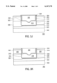
- FIG. 1 is a cross-sectional view of the device structure of a conventional nonvolatile memory device 100 including a substrate 102 of a semiconductor crystal such as silicon.
- the device 100 further includes a channel region 104, a source region 106, a drain region 108, a floating gate dielectric layer 110, a floating gate electrode 112, an inter-gate dielectric layer 114, and a control gate electrode 116.
- the floating gate dielectric layer 110 isolates the floating gate electrode 112 from the underlying substrate 102 while the inter-gate dielectric 114 isolates the control gate electrode 116 from the floating gate electrode 112. As shown in FIG. 1, the floating gate dielectric layer 110, the floating gate electrode 112, the inter-gate dielectric layer 114, and the control gate electrode 116 are all disposed on the surface of the substrate 102.
- a semiconductor device for low power applications is fabricated to include a fully recessed cell structure comprising a trenched floating gate, a trenched control gate, and a single wrap around buried drain region.
- a fully recessed trenched gate structure embodying the principles of the present invention provides a substantially planar topography that improves the packing density and scaleability of the device. Additionally, the present invention provides low substrate current programming and an enhanced erase operation.
- a fully recessed trenched gate device structure for a non-volatile semiconductor device includes a well junction region and a trench etched into the well junction region.
- the fully recessed trenched gate structure comprises a trenched floating gate and a trenched control gate both formed in the trench.
- the trenched floating gate is electrically isolated from the trench by a trench-to-gate dielectric layer formed on substantially vertical sidewalls and on a bottom surface inside the trench.
- An inter-gate dielectric layer is formed on the trenched floating gate and electrically isolates the trenched floating gate from the trenched control gate.
- the trenched control gate is formed inside the trench on the inter-gate dielectric layer and in a preferred embodiment, has a top surface which is substantially planar with a surface of the substrate.
- a buried source region and a buried drain region are also formed in the well junction region and are laterally separated by the fully recessed trenched gate structure.
- the upper boundaries of the buried source region and the buried drain region are of approximately the same depth as the top surface of the trenched floating gate.
- the buried drain region has a lower boundary which partially extends laterally underneath the bottom surface of the trench to form a drain junction disposed along portions of the sidewall and bottom of the trench.
- the buried source region has a lower boundary which is approximately less than the depth of the trench.
- the buried source region has a lower boundary which partially extends laterally underneath the bottom surface of the trench to form a source junction disposed along portions of the sidewall and bottom of the trench.
- the buried drain region has a lower boundary which is approximately less than the depth of the trench.
- sidewall dopings of one conductivity type are formed in the semiconductor substrate.
- the sidewall dopings are immediately contiguous the vertical sidewalls of the trench and immediately contiguous the substrate surface.
- the depth of the sidewall dopings is approximately equal to or greater than the depth of the trenched control gate and partially extend into the buried source and buried drain regions.
- an implanted region of one conducting type is formed in the semiconductor substrate.
- the implanted region is laterally separated by the trench and is immediately contiguous the substantially vertical sidewalls of the trench, the substrate surface and the upper boundaries of the buried source region and the buried drain region.
- a fully recessed device structure is formed in a semiconductor substrate using an MOS fabrication process according to which a well junction region is formed in the substrate.
- a trench is then etched into the well junction region.
- a trench-to-gate insulating layer is formed on substantially upright vertical sidewalls and on a bottom surface inside the trench.
- a trenched floating gate is fabricated by first depositing a layer of polysilicon over the substrate and then etching the polysilicon layer.
- An inter-gate dielectric is then deposited on the trenched floating gate inside the trench to isolate the two gate electrodes.
- the trenched control gate is formed by first depositing a layer of polysilicon over the substrate and then planarizing the polysilicon layer until it is substantially planar with the substrate surface.
- a buried source region and a buried drain region are formed in the well junction region.
- sidewall dopings are formed in the substrate and are immediately contiguous the vertical sidewalls of the trench and the substrate surface.
- FIG. 1 is a cross-sectional view of a conventional non-volatile device.
- FIGS. 2A-2D are cross-sectional views of a device structure embodying the principles of the present invention.
- FIGS. 3A-3N are cross-sectional views of a semiconductor substrate in various stages of processing in accordance with one embodiment of the present invention.
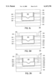
- FIG. 2A is a cross-sectional view of one embodiment of a non-volatile device embodying the principles of the present invention.
- FIG. 2A shows a semiconductor structure 200 including a substrate 202 of monocrystalline silicon semiconductor material.
- the substrate 202 is preferably n-doped or provided with an n-well to a suitable threshold voltage level in accordance with conventional silicon semiconductor fabrication techniques.
- Semiconductor structure 200 also includes a well junction region 203, preferably p-type, formed in semiconductor substrate 202.
- Structure 200 also includes a channel region 204, a buried source region 206, a buried drain region 208, a trench 210, and a trench-to-gate insulating layer 212.
- Structure 200 further includes a trenched floating gate electrode 218, an inter-gate dielectric layer 220 formed in trench 210, and a trenched control gate electrode 222.
- Trenched control gate electrode 222 is formed over inter-gate dielectric layer 220 and in a preferred embodiment has a top surface which is substantially planar with a top surface of substrate 202.
- a layer of tungsten silicide 224 is formed on the top surface of substrate 202.
- Source and drain contacts 226 are also formed in the substrate and partially extend into the buried source and buried drain regions 206, 208.
- Buried source region 206 and buried region 208 are diffusion regions of semiconductor material that are doped with impurities that have a conductivity opposite to the conductivity of well junction region 203.
- the opposite conductivity type for buried source region 206 and buried drain region 208 is n-type.
- buried source region 206 and buried drain region 208 are doped with "donor" or n-type impurities of phosphorous, arsenic or the like in conventional manner with a dose range on the order of approximately 5E14 atoms cm -2 to approximately 1E16 atoms cm -2 .
- Buried source region 206 and buried drain region 208 are laterally separated by trench 210 and are immediately contiguous the substantially upright vertical sidewalls of trench 210.
- Buried source region 206 and buried drain region 208 are diffusion regions which have an upper boundary below the top surface of the substrate.
- the upper boundaries, i.e., the boundaries closest to the top surface of the semiconductor substrate, of buried source region 206 and buried drain region 208 are disposed at approximately the same depth as the top surface of trenched floating gate 218.
- buried source region 206 has a lower boundary, i.e.
- the diffusion of buried source region 206 disposed along portions of the lower sidewall and bottom of trench 210 is a corner-limiting diffusion process which improves the uniformity and controllability of the lateral diffusion of the buried source region 206 under the trenched gate structure. This corner-limiting diffusion process is described below in more detail with reference to FIG. 3J.
- channel region 204 is immediately contiguous the buried source region 206 disposed underneath the bottom of the trench.
- buried drain region 208 has a lower boundary which partially extends laterally underneath the bottom surface of the trench to form a drain junction disposed along portions of the lower sidewall and bottom of trench 210 while the lower boundary of buried source region 206 is approximately less than the depth of trench 210 as shown in FIG. 2B.
- the diffusion of buried drain region 208 that is disposed along portions of the lower sidewall and bottom of trench 210 is a corner-limiting diffusion process which improves the uniformity and controllability of the lateral diffusion of buried drain region 208 under the trenched gate structure. This corner-limiting diffusion process is described below in more detail with reference to FIG. 3J.
- channel region 204 is immediately contiguous the buried drain region 208 disposed underneath the bottom of the trench.
- Channel region 204 is an implanted region formed beneath the bottom surface of trench 210.
- channel region 204 is a depletion type channel region.
- trench 210 is between approximately 100 ⁇ and 5000 ⁇ wide and from approximately 100 ⁇ to 5000 ⁇ deep.
- Trench-to-gate insulating layer 212 is formed on substantially upright vertical sidewalls and a bottom surface inside trench 210 and has preferably a high dielectric constant (K).
- K dielectric constant
- the thickness of trench-to-gate insulating layer 212 is scaled according to the width of trench 210 to comprise only an insignificant part of the dimensions of trench 210.
- Trench-to-gate insulting layer 212 may comprise a uniform thickness on the vertical sidewalls and the bottom surface of trench 210. Alternatively, the thickness of trench-to-gate insulating layer 212 may be thicker on the vertical sidewalls inside trench 210 than on the bottom surface inside the trench. Trench-to-gate insulating layer 212 is preferably a nitridized thermal oxide, a deposited high temperature oxide (HTO), or composited dielectric films with a K approximately equal to or greater than 4.0.
- HTO deposited high temperature oxide
- trench-to-gate insulating layer 212 may comprise either one film formed on both the substantially upright vertical sidewalls and the bottom surface inside trench 210 or it may comprise one type of film formed on the substantially upright vertical sidewalls inside trench 210 and a different film formed on the bottom surface inside trench 210.
- Trenched floating gate electrode 218 is formed inside trench 210 on trench-to-gate insulating layer 212 which electrically isolates it from trench 210.
- Trenched floating gate electrode 218 is a conductive material such as polysilicon, preferably doped with n-type material, or a layer of polysilicide, and has a final thickness which is approximately equal to one half of the depth of trench 210.
- Inter-gate dielectric layer 220 is formed on trenched floating gate electrode 218 inside trench 210 and electrically isolates trenched floating gate electrode 218 from trenched control gate electrode 222. In one embodiment, an additional spacer dielectric may also be formed at the upper sidewalls inside trench 210 in order to further decouple the trenched control gate from the buried source and buried drain regions.
- Inter-gate dielectric layer 220 is preferably a high K dielectric material, such as an Oxide-Nitride-Oxide (ONO) layer formed in conventional manner on trenched floating gate electrode 218 inside trench 210.
- Trenched control gate electrode 222 is a conductive material, such as polysilicon, preferably doped with n-type material, or polysilicide formed on inter-gate dielectric layer 220 inside trench 210 and preferably, has a top surface which is substantially planar with a top surface of substrate 202. Trenched control gate electrode 222 substantially fills the remainder of trench 210 and has a final thickness which is approximately equal to one half the depth of trench 210. In a preferred embodiment, a layer of tungsten silicide 224 is also formed on the top surface of trenched control gate electrode 222. Contacts 226 to buried source region 206 and buried drain region 208 may also be formed in the semiconductor substrate and partially extend into buried source region 206 and buried source region 208.
- One advantage of the present invention is the substantially planar topography of the fully recessed device structure.
- the substantially planar topography improves the packing density and scaleability of the device as well as the manufacturability of the device. Because the trenched floating gate electrode and the trenched control gate electrode are both formed in a single trench etched into the semiconductor substrate, the fully recessed device structure is self-aligned. In other words, the trenched control gate electrode and the trenched floating gate electrode are self-aligned, and the trenched gates and the source and drain regions are self-aligned.
- Embodiments employing the principles of the present invention also provide low substrate current programming suitable for low power applications by using Fowler-Nordheim tunneling for both program and erase operations. While the operation of the present invention will be described in terms of an n-p-n device, it should be recognized that the operation of a pnp device is also possible by biasing the electrodes with an opposite polarity. All cells in a npr device may be globally programmed by positively biasing trenched control gate electrode 222 and grounding all other nodes, i.e. buried drain region 208, and buried source region 206 and substrate 202 so that channel region 204 is turned on.
- Devices employing the principles of the present invention provide selective erasure of the individual cells in a device.
- the device is erased by negatively biasing trenched control gate electrode 222 so that channel region 204 is turned off, and positively biasing buried drain region 208 which permits a higher drain bias without generating excess leakage.
- Source region 206 and well junction region 203 are left floating.
- trenched control gate electrode 222 is grounded. The selective erase improves the erase efficiency of the device and controls and reduces device leakages and the sensitivity to over-erase problems.
- Devices embodying the principles of the present invention are read by positively biasing trenched control gate electrode 222 and drain region 208, and grounding source region 206 and well junction region 203.
- Devices embodying the principles of the present invention may also be used for high speed applications by using hot carrier injection for programming the device and Fowler-Nordheim techniques for erasing the device.
- Individual cells can be selectively programmed by positively biasing trenched control gate electrode 222 and drain region 208 and grounding source region 206 and well junction region 203.
- the trenched control gate electrode 222 of unselected cells in an array are grounded.
- the device may be globally erased by either grounding or negatively biasing trenched control gate electrode 222 and positively biasing all other nodes.
- FIG. 2C is another embodiment of the present invention including sidewall dopings.
- sidewall dopings 228 are formed in the semiconductor substrate by implanting the substrate at a large angle, preferably 15 to 75 degrees, in conventional manner with dopant impurities of one conductivity type.
- the convention for determining the angle of an implant is relative to the axis which is normal to the top surface of the substrate. In other words, 0 degrees refers to an implant along the axis which is normal to the top surface of the substrate and 90 degrees refers to an implant which is parallel to the top surface of the substrate.
- Sidewall dopings 228 are immediately contiguous the upper vertical sidewalls of trench 210 and the substrate surface, as shown in FIG. 2C.
- the depth of sidewall dopings 228 is approximately equal to or greater than the depth of trenched control gate 222 but less than the depth of trench 210 to allow electrons to flow to and from buried drain region 208 and from and to trenched floating gate electrode 218 through the sidewalls of trench 210 for program and erase operations, and partially extend into buried source region 206 and buried drain region 208.
- sidewall dopings 228 are preferably deep enough to shield trenched control gate electrode 222 from buried source and buried drain regions 206, 208.
- Sidewall dopings 228 have a conductivity which is the same as the conductivity of well junction region 203.
- Sidewall dopings 228 in accordance with the present invention minimize the sensitivity to misalignments between trenched control gate 222 and the buried source and buried drain regions 206, 208 by reducing the coupling between trenched control gate electrode 222 and buried source region 206 and buried drain region 208. Additionally, sidewall dopings 228 reduce leakages of electrons from the trenched gate electrodes through the sidewalls of the trench.
- FIG. 2D is a cross-sectional view of yet another embodiment of the present invention.
- an implanted region 230 preferably doped with "acceptor" or p-type impurities, is formed in the semiconductor substrate.
- Implanted region 230 is laterally separated by trench 210 and is immediately contiguous the vertical sidewalls of trench 210, the substrate surface and the upper boundaries of buried source region 206 and buried drain region 208 as shown in FIG. 2D.
- Implanted region 230 is formed in the semiconductor substrate by implanting the substrate in conventional manner preferably after trenched control gate 222 is formed.
- the depth of implanted region 230 is approximately equal to or greater than the depth of trenched control gate 222 and is determined by the ion implant used to form buried source region 206 and buried drain region 208. In other words, the upper boundary of buried source region 206 and buried drain region 208 is immediately contiguous to the lower boundary of implanted region 230. Thus, implanted region 230 is preferably deep enough to shield trenched control gate electrode 222 from buried source and buried drain regions 206, 208.
- Implanted region 230 is preferably doped with "acceptor" or p-type impurities, such as boron, and are formed using an ion implant in conventional manner with an implant dose range on the order of 1E12 atoms cm -2 to on the order of 1E15 atoms cm -2 .
- Implanted region 230 in accordance with the present invention minimizes the coupling between trenched control gate electrode 222 and buried source region 206 and buried drain region 208. Additionally, implanted region 230 reduces leakages of electrons from the trenched gate electrodes through the sidewalls of trench 210.
- a layer of tungsten silicide or tungsten is used to interconnect the trenched control gates of multiple device structures in a semiconductor device.
- the method for forming the tungsten silicide or tungsten interconnects is described below in more detail with reference to FIG. 3I.
- FIG. 3A-3N are cross-sectional views of the semiconductor substrate in various stages of processing in accordance with one embodiment of the present invention. While the present invention will now be described in terms of fabricating a single device structure, it should be recognized that the underlying process of the present invention may be employed to fabricate multiple devices on a single substrate.
- FIG. 3A is a cross-sectional view of a semiconductor wafer 300 comprising a substrate 302, a well-junction region 303, a first pad oxide layer 304, a nitride layer 306, a trench 308, a second pad oxide layer 309 and a channel region 310.
- the substrate 302 is preferably an n-doped silicon substrate cut from a single silicon crystal.
- Well junction region 303 is preferably p-doped.
- First pad oxide layer 304 is approximately 100 ⁇ thick and provides stress relief between substrate 302 and nitride layer 306.
- Nitride layer 306 has a thickness of approximately 1500 ⁇ and preferably comprises silicon nitride (Si 3 N 4 ).
- Nitride layer 306 serves as a masking layer or etch stop for subsequent oxidation, chemical-mechanical polishing (CMP), and etching steps.
- CMP chemical-mechanical polishing
- the nitride layer 306 and oxide layer 304 sandwich can also be used as an isolation mask material. Thus, the steps for forming the fully recessed gate trench may be integrated into conventional CMOS process flows.
- First pad oxide layer 304 and nitride layer 306 may be deposited in conventional manner by chemical vapor deposition (CVD) or other techniques.
- Trench 308 is formed in conventional manner using a reactive ion etch (RIE) to remove the silicon substrate.
- RIE reactive ion etch
- the trench etching process may include multiple steps such as a nitride etch, an oxide etch and a high selectivity silicon to oxide etch.
- Second pad oxide layer 309 is grown in conventional manner inside trench 308.
- second pad oxide layer 309 has a thickness of approximately 200 ⁇ when trench 308 is approximately 3000 ⁇ to 5000 ⁇ wide.
- Channel region 310 is preferably formed using ion implantation of phosphorous in conventional manner with a dose range on the order of approximately 1E10 atoms cm -2 to on the order of 1E13 atoms cm -2 and an energy of approximately 1 keV to 60 keV at an angle of approximately 0 degrees in order to form a depletion type channel region to achieve a low threshold voltage.
- channel region 310 may be formed using an ion implantation of boron in conventional manner.
- FIG. 3B is a cross-sectional view of semiconductor wafer 300 following formation of trench-to-gate insulating layer 314.
- second pad oxide layer 309 may be removed in conventional manner prior to forming trench-to-gate insulating layer 314.
- an insulating layer such as a layer of thermally grown or deposited oxide, preferably nitridized, is formed in conventional manner on the substantially upright vertical sidewalls and on the bottom surface inside trench 308.
- the nitridized oxide has a K higher than about 4.0.
- trench-to-gate insulating layer 314 may be formed with a different thickness on the substantially upright vertical sidewalls inside trench 310 than the thickness on the bottom surface inside trench 310.
- FIG. 3C is a cross-sectional view of semiconductor wafer 300 following deposition of a layer of polysilicon 318.
- the thickness of polysilicon layer 318 is selected according to the depth of trench 308. In a preferred embodiment of the invention, the thickness of polysilicon layer 318 is between about 1000 ⁇ and 10,000 ⁇ .
- polysilicon layer 318 may be formed in conventional manner by low pressure chemical vapor deposition (LPCVD) and can be doped in situ in conventional manner.
- LPCVD low pressure chemical vapor deposition
- Polysilicon layer 318 subsequently undergoes a polish, a plasma etch or a combination of a polish and plasma etch in conventional manner to remove portions of the polysilicon.
- FIG. 3D is a cross-sectional view of semiconductor wafer 300 following a plasma etch of polysilicon layer 318.
- sidewall dopings are formed in the semiconductor substrate.
- semiconductor wafer 300 is implanted with dopant impurities of one conductivity type to form sidewall dopings 312.
- FIG. 3E is a cross sectional view of semiconductor wafer 300 following implantation of sidewall dopings 312.
- boron is implanted at a large angle around 15 to 75 degrees with a dose range on the order of approximately 1E13 atoms cm -2 to on the order of 1E15 atoms cm -2 and with an energy ranging from approximately 1 to 60 keV.
- sidewall dopings 312 may also be formed after forming inter-gate dielectric layer 320.
- a trench sidewall spacer 319 is formed at the upper vertical surfaces of trench-to-gate insulating layer 314 inside trench 308 in order to further shield the trenched control gate electrode from the source and drain regions.
- Trench sidewall spacer 319 is immediately contiguous to both trench-to-gate insulating layer 314 and a portion of a top surface of trenched floating gate electrode 318.
- Inter-gate dielectric layer 320 is then deposited on wafer 300 to form an insulating layer on trenched floating gate electrode 318 and trench sidewall spacer 319 inside trench 308.
- FIG. 3F is a cross-sectional view of semiconductor wafer 300 after forming inter-gate dielectric 320.
- the inter-gate dielectric 320 is preferably an oxide-nitride-oxide (ONO) layer formed in conventional manner. In one embodiment, an additional spacer dielectric may be formed at the vertical sidewalls inside trench 308 in order to further shield the trenched control gate electrode from the source and drain regions.
- a second layer of polysilicon or a layer of polysilicide 322 is deposited in conventional manner to form the trenched control gate for non-volatile devices.
- FIG. 3G is a cross-sectional view of semiconductor wafer 300 after second layer of polysilicon 322 has been deposited. The final thickness of second polysilicon layer or layer of polysilicide 322 is approximately one half the depth of trench 308.
- FIG. 3H is a cross-sectional view of semiconductor wafer 300 following planarization of second layer of polysilicon 322.
- Second layer of polysilicon 322 is planarized by using conventional techniques such as a chemical-mechanical planarization (CMP) with nitride layer 306 acting as an etch stop.
- CMP chemical-mechanical planarization
- FIG. 3I is a cross-sectional view of semiconductor wafer 322 after formation of tungsten silicide 324 on trenched control gate 322.
- tungsten silicide layer 324 or a layer of tungsten can be patterned in conventional manner to interconnect multiple devices.
- oxide layer 304 and nitride layer 306 protect the other regions of the device structure.
- Tungsten silicide layer 324 on the top surface of trenched control gate 323 provides additional protection for trenched control gate 322 during the subsequent formation of the buried source region and the buried drain region. Thereafter, inter-gate dielectric layer 320 and nitride layer 306 outside the trenched gate region are removed in conventional manner.
- FIG. 3J is a cross-sectional view of semiconductor wafer 300 after formation of buried source region 326 and buried drain region 328.
- multiple ion implantations of arsenic, phosphorous, or a combination of arsenic and phosphorous with a dose range on the order of 5E14 atoms cm -2 to on the order of 1E16 atoms cm -2 are performed at different implant energies.
- the upper boundaries of buried source region 326 and buried drain region 328 are approximately at the same depth as the top surface of the trenched floating gate.
- buried source region 326 is formed using a corner-limiting diffusion process to form a lower boundary which partially extends laterally underneath the bottom surface of the trench to form a source junction disposed along portions of the lower sidewall and bottom of trench 308 while buried drain region 328 is implanted such that the lower boundary of buried drain region 328 is less than the depth of the trench.
- buried drain region 328 is formed using a corner-limiting diffusion process to form a lower boundary which partially extends laterally underneath the bottom surface of the trench to form a drain junction disposed along portions of the lower sidewall and bottom of trench 308 while buried source region 326 is implanted such that the lower boundary of buried source region 326 is less than the depth of the trench.
- the corner-limiting diffusion process is primarily due to the corner effects of the trench, i.e., where the lower sidewall and bottom of the trench intersect.
- the source and drain implants are immediately contiguous the sidewalls of the trench with the deepest "as-implanted" dopant peak of the buried source and buried drain regions being disposed at substantially the same depth as the depth of the trench before a thermal anneal.
- the lateral diffusion of buried source and buried drain junctions beneath the bottom surface of the trench is constrained by the amount of dopants available at the bottom corner, i.e., the intersection of the lower sidewall and bottom of the trench, and by the radial nature of the diffusion process. As a result, only a low percentage of dopant diffuses around the bottom corner of the trench, thus resulting in a corner-limiting process.
- semiconductor wafer 300 is implanted with dopant impurities of one conductivity type to form implanted region 330.
- Implanted region 330 is formed by first performing a shallow implant in conventional manner with dopant impurities of one conductivity type, preferably p-type.
- FIG. 3K is a cross sectional view of semiconductor wafer 300 following a shallow implant.
- boron is implanted with a dose range on the order of approximately 1E12 atoms cm -2 to on the order of 1E15 atoms cm -2 and with an energy ranging from approximately 100 eV to 60 keV.
- the resulting implanted region is immediately contiguous the vertical sidewalls of the trench 308, the substrate surface and the upper boundaries of buried source region 326 and buried drain region 328.
- Interlayer dielectric 332 is a cross-sectional view of semiconductor wafer 300 following deposition of interlayer dielectric 332.
- Interlayer dielectric 332 may be any number of films such as Tetra-Ethyl-Ortho-Silicate (TEOS), a high temperature oxide (HTO), or a low temperature oxide (LTO).
- TEOS Tetra-Ethyl-Ortho-Silicate
- HTO high temperature oxide
- LTO low temperature oxide
- FIG. 3M is a cross-sectional view of semiconductor wafer 300 after forming contact openings 334.
- Contact openings 334 are preferably formed using an RIE etch in conventional manner.
- FIG. 3N is a cross-sectional view of semiconductor wafer 300 after formation of contacts 336 to buried source and buried drain regions 326, 328 and final formation of sidewall dopings 330. Finally, standard processing techniques are used to complete processing of semiconductor wafer 300.
Abstract
Description
Claims (14)
Priority Applications (2)
| Application Number | Priority Date | Filing Date | Title |
|---|---|---|---|
| US09/052,060 US6147378A (en) | 1998-03-30 | 1998-03-30 | Fully recessed semiconductor device and method for low power applications with single wrap around buried drain region |
| US09/470,568 US6225161B1 (en) | 1998-03-30 | 1999-12-22 | Fully recessed semiconductor method for low power applications with single wrap around buried drain region |
Applications Claiming Priority (1)
| Application Number | Priority Date | Filing Date | Title |
|---|---|---|---|
| US09/052,060 US6147378A (en) | 1998-03-30 | 1998-03-30 | Fully recessed semiconductor device and method for low power applications with single wrap around buried drain region |
Related Child Applications (1)
| Application Number | Title | Priority Date | Filing Date |
|---|---|---|---|
| US09/470,568 Division US6225161B1 (en) | 1998-03-30 | 1999-12-22 | Fully recessed semiconductor method for low power applications with single wrap around buried drain region |
Publications (1)
| Publication Number | Publication Date |
|---|---|
| US6147378A true US6147378A (en) | 2000-11-14 |
Family
ID=21975188
Family Applications (2)
| Application Number | Title | Priority Date | Filing Date |
|---|---|---|---|
| US09/052,060 Expired - Fee Related US6147378A (en) | 1998-03-30 | 1998-03-30 | Fully recessed semiconductor device and method for low power applications with single wrap around buried drain region |
| US09/470,568 Expired - Lifetime US6225161B1 (en) | 1998-03-30 | 1999-12-22 | Fully recessed semiconductor method for low power applications with single wrap around buried drain region |
Family Applications After (1)
| Application Number | Title | Priority Date | Filing Date |
|---|---|---|---|
| US09/470,568 Expired - Lifetime US6225161B1 (en) | 1998-03-30 | 1999-12-22 | Fully recessed semiconductor method for low power applications with single wrap around buried drain region |
Country Status (1)
| Country | Link |
|---|---|
| US (2) | US6147378A (en) |
Cited By (19)
| Publication number | Priority date | Publication date | Assignee | Title |
|---|---|---|---|---|
| US6239465B1 (en) * | 1999-01-27 | 2001-05-29 | Fujitsu, Ltd. | Non-volatile semiconductor memory device having vertical transistors with the floating and control gates in a trench and fabrication method therefor |
| US6284608B1 (en) * | 2000-02-01 | 2001-09-04 | Advanced Micro Devices, Inc. | Method for making accumulation mode N-channel SOI |
| US6465836B2 (en) * | 2001-03-29 | 2002-10-15 | Taiwan Semiconductor Manufacturing Co., Ltd | Vertical split gate field effect transistor (FET) device |
| US6469345B2 (en) * | 2000-01-14 | 2002-10-22 | Denso Corporation | Semiconductor device and method for manufacturing the same |
| US20030001204A1 (en) * | 2001-06-27 | 2003-01-02 | Mitsubishi Denki Kabushiki Kaisha | Semiconductor device and method for fabricating the same |
| US20030148575A1 (en) * | 2000-12-19 | 2003-08-07 | Micron Technology, Inc. | Methods of accessing floating-gate memory cells having underlying source-line connections |
| US20040071016A1 (en) * | 2000-11-02 | 2004-04-15 | Oliver Gehring | Semiconductor memory cell and method for producing the same |
| US20040248407A1 (en) * | 2003-06-05 | 2004-12-09 | Chi-Wen Liu | Displacement method to grow cu overburden |
| US6864532B2 (en) | 2000-01-14 | 2005-03-08 | Denso Corporation | Semiconductor device and method for manufacturing the same |
| US20050151185A1 (en) * | 2003-12-31 | 2005-07-14 | Jung Jin H. | Semiconductor device and fabricating method thereof |
| US20060186458A1 (en) * | 2005-02-23 | 2006-08-24 | Micron Technology,Inc. | Germanium-silicon-carbide floating gates in memories |
| US20070210403A1 (en) * | 2006-03-07 | 2007-09-13 | Micron Technology, Inc. | Isolation regions and their formation |
| US7372096B2 (en) | 2001-08-30 | 2008-05-13 | Micron Technology, Inc. | Programmable array logic or memory with p-channel devices and asymmetrical tunnel barriers |
| US7443715B2 (en) | 2001-08-30 | 2008-10-28 | Micron Technology, Inc. | SRAM cells with repressed floating gate memory, low tunnel barrier interpoly insulators |
| US7465983B2 (en) | 2001-08-30 | 2008-12-16 | Micron Technology, Inc. | Low tunnel barrier insulators |
| US7545674B2 (en) | 2001-08-30 | 2009-06-09 | Micron Technology, Inc. | Flash memory with low tunnel barrier interpoly insulators |
| US7572695B2 (en) | 2005-05-27 | 2009-08-11 | Micron Technology, Inc. | Hafnium titanium oxide films |
| US20120056258A1 (en) * | 2010-09-06 | 2012-03-08 | Shu-Lu Chen | Electrical switch using gated resistor structures and three-dimensional integrated circuits using the same |
| CN108321192A (en) * | 2018-02-05 | 2018-07-24 | 电子科技大学 | A kind of two-way trench gate charge storage type IGBT and preparation method thereof |
Families Citing this family (3)
| Publication number | Priority date | Publication date | Assignee | Title |
|---|---|---|---|---|
| US6417050B1 (en) * | 2000-08-07 | 2002-07-09 | Semiconductor Components Industries Llc | Semiconductor component and method of manufacture |
| US8058687B2 (en) * | 2007-01-30 | 2011-11-15 | Alpha & Omega Semiconductor, Ltd. | Split gate with different gate materials and work functions to reduce gate resistance of ultra high density MOSFET |
| US8664713B2 (en) * | 2008-12-31 | 2014-03-04 | Stmicroelectronics S.R.L. | Integrated power device on a semiconductor substrate having an improved trench gate structure |
Citations (15)
| Publication number | Priority date | Publication date | Assignee | Title |
|---|---|---|---|---|
| US35810A (en) * | 1862-07-08 | Improved clothes-wringer | ||
| US4271418A (en) * | 1979-10-29 | 1981-06-02 | American Microsystems, Inc. | VMOS Memory cell and method for making same |
| US4835741A (en) * | 1986-06-02 | 1989-05-30 | Texas Instruments Incorporated | Frasable electrically programmable read only memory cell using a three dimensional trench floating gate |
| US5146426A (en) * | 1990-11-08 | 1992-09-08 | North American Philips Corp. | Electrically erasable and programmable read only memory with trench structure |
| US5315142A (en) * | 1992-03-23 | 1994-05-24 | International Business Machines Corporation | High performance trench EEPROM cell |
| US5341342A (en) * | 1992-12-18 | 1994-08-23 | National Semiconductor Corporation | Flash memory cell structure |
| US5429970A (en) * | 1994-07-18 | 1995-07-04 | United Microelectronics Corporation | Method of making flash EEPROM memory cell |
| US5488244A (en) * | 1995-02-27 | 1996-01-30 | Chartered Simiconductor Manufacturing Pte Ltd. | Electrically erasable and programmable read only memory cell |
| US5729496A (en) * | 1994-07-30 | 1998-03-17 | Lg Semicon Co., Ltd. | Nonvolatile semiconductor memory element and method for fabricating the same |
| US5770484A (en) * | 1996-12-13 | 1998-06-23 | International Business Machines Corporation | Method of making silicon on insulator buried plate trench capacitor |
| US5801075A (en) * | 1996-10-30 | 1998-09-01 | Advanced Micro Devices, Inc. | Method of forming trench transistor with metal spacers |
| US5854114A (en) * | 1997-10-09 | 1998-12-29 | Advanced Micro Devices, Inc. | Data retention of EEPROM cell with shallow trench isolation using thicker liner oxide |
| US5859459A (en) * | 1996-04-03 | 1999-01-12 | Sony Corporation | Semiconductor memory device and method of manufacturing the same |
| US5915180A (en) * | 1994-04-06 | 1999-06-22 | Denso Corporation | Process for producing a semiconductor device having a single thermal oxidizing step |
| US5923063A (en) * | 1998-02-19 | 1999-07-13 | Advanced Micro Devices, Inc. | Double density V nonvolatile memory cell |
Family Cites Families (5)
| Publication number | Priority date | Publication date | Assignee | Title |
|---|---|---|---|---|
| US4979004A (en) | 1988-01-29 | 1990-12-18 | Texas Instruments Incorporated | Floating gate memory cell and device |
| DE3816358A1 (en) | 1988-05-13 | 1989-11-23 | Eurosil Electronic Gmbh | NON-VOLATILE STORAGE CELL AND METHOD FOR THE PRODUCTION THEREOF |
| US5281548A (en) | 1992-07-28 | 1994-01-25 | Micron Technology, Inc. | Plug-based floating gate memory |
| US5990515A (en) * | 1998-03-30 | 1999-11-23 | Advanced Micro Devices, Inc. | Trenched gate non-volatile semiconductor device and method with corner doping and sidewall doping |
| US5897343A (en) * | 1998-03-30 | 1999-04-27 | Motorola, Inc. | Method of making a power switching trench MOSFET having aligned source regions |
-
1998
- 1998-03-30 US US09/052,060 patent/US6147378A/en not_active Expired - Fee Related
-
1999
- 1999-12-22 US US09/470,568 patent/US6225161B1/en not_active Expired - Lifetime
Patent Citations (15)
| Publication number | Priority date | Publication date | Assignee | Title |
|---|---|---|---|---|
| US35810A (en) * | 1862-07-08 | Improved clothes-wringer | ||
| US4271418A (en) * | 1979-10-29 | 1981-06-02 | American Microsystems, Inc. | VMOS Memory cell and method for making same |
| US4835741A (en) * | 1986-06-02 | 1989-05-30 | Texas Instruments Incorporated | Frasable electrically programmable read only memory cell using a three dimensional trench floating gate |
| US5146426A (en) * | 1990-11-08 | 1992-09-08 | North American Philips Corp. | Electrically erasable and programmable read only memory with trench structure |
| US5315142A (en) * | 1992-03-23 | 1994-05-24 | International Business Machines Corporation | High performance trench EEPROM cell |
| US5341342A (en) * | 1992-12-18 | 1994-08-23 | National Semiconductor Corporation | Flash memory cell structure |
| US5915180A (en) * | 1994-04-06 | 1999-06-22 | Denso Corporation | Process for producing a semiconductor device having a single thermal oxidizing step |
| US5429970A (en) * | 1994-07-18 | 1995-07-04 | United Microelectronics Corporation | Method of making flash EEPROM memory cell |
| US5729496A (en) * | 1994-07-30 | 1998-03-17 | Lg Semicon Co., Ltd. | Nonvolatile semiconductor memory element and method for fabricating the same |
| US5488244A (en) * | 1995-02-27 | 1996-01-30 | Chartered Simiconductor Manufacturing Pte Ltd. | Electrically erasable and programmable read only memory cell |
| US5859459A (en) * | 1996-04-03 | 1999-01-12 | Sony Corporation | Semiconductor memory device and method of manufacturing the same |
| US5801075A (en) * | 1996-10-30 | 1998-09-01 | Advanced Micro Devices, Inc. | Method of forming trench transistor with metal spacers |
| US5770484A (en) * | 1996-12-13 | 1998-06-23 | International Business Machines Corporation | Method of making silicon on insulator buried plate trench capacitor |
| US5854114A (en) * | 1997-10-09 | 1998-12-29 | Advanced Micro Devices, Inc. | Data retention of EEPROM cell with shallow trench isolation using thicker liner oxide |
| US5923063A (en) * | 1998-02-19 | 1999-07-13 | Advanced Micro Devices, Inc. | Double density V nonvolatile memory cell |
Cited By (46)
| Publication number | Priority date | Publication date | Assignee | Title |
|---|---|---|---|---|
| US6391721B2 (en) | 1999-01-27 | 2002-05-21 | Fujitsu Limited | Non-volatile semiconductor memory device having vertical transistors and fabrication method therefor |
| US6239465B1 (en) * | 1999-01-27 | 2001-05-29 | Fujitsu, Ltd. | Non-volatile semiconductor memory device having vertical transistors with the floating and control gates in a trench and fabrication method therefor |
| US6469345B2 (en) * | 2000-01-14 | 2002-10-22 | Denso Corporation | Semiconductor device and method for manufacturing the same |
| US7354829B2 (en) | 2000-01-14 | 2008-04-08 | Denso Corporation | Trench-gate transistor with ono gate dielectric and fabrication process therefor |
| US20050090060A1 (en) * | 2000-01-14 | 2005-04-28 | Takaaki Aoki | Method for manufacturing semiconductor device |
| US6864532B2 (en) | 2000-01-14 | 2005-03-08 | Denso Corporation | Semiconductor device and method for manufacturing the same |
| US6284608B1 (en) * | 2000-02-01 | 2001-09-04 | Advanced Micro Devices, Inc. | Method for making accumulation mode N-channel SOI |
| US20040071016A1 (en) * | 2000-11-02 | 2004-04-15 | Oliver Gehring | Semiconductor memory cell and method for producing the same |
| US6940121B2 (en) * | 2000-11-02 | 2005-09-06 | Infineon Technology Ag | Semiconductor memory cell |
| US6774426B2 (en) | 2000-12-19 | 2004-08-10 | Micron Technology, Inc. | Flash cell with trench source-line connection |
| US7176077B2 (en) | 2000-12-19 | 2007-02-13 | Micron Technology, Inc. | Methods of forming memory cells and arrays having underlying source-line connections |
| US6721206B2 (en) | 2000-12-19 | 2004-04-13 | Micron Technology, Inc. | Methods of accessing floating-gate memory cells having underlying source-line connections |
| US20040262671A1 (en) * | 2000-12-19 | 2004-12-30 | Micron Technology, Inc. | Flash cell with trench source-line connection |
| US20030148575A1 (en) * | 2000-12-19 | 2003-08-07 | Micron Technology, Inc. | Methods of accessing floating-gate memory cells having underlying source-line connections |
| US20050148141A1 (en) * | 2000-12-19 | 2005-07-07 | Micron Technology, Inc. | Methods of forming memory cells and arrays having underlying source-line connections |
| US20070117299A1 (en) * | 2000-12-19 | 2007-05-24 | Micron Technology, Inc. | Memory cells having underlying source-line connections |
| US6929993B2 (en) | 2000-12-19 | 2005-08-16 | Micron Technology, Inc. | Methods of forming memory cells and arrays having underlying source-line connections |
| US6949791B2 (en) | 2000-12-19 | 2005-09-27 | Micron Technology, Inc. | Flash cell with trench source-line connection |
| US6465836B2 (en) * | 2001-03-29 | 2002-10-15 | Taiwan Semiconductor Manufacturing Co., Ltd | Vertical split gate field effect transistor (FET) device |
| US6700159B2 (en) * | 2001-06-27 | 2004-03-02 | Renesas Technology Corp. | Semiconductor device comprising trench-isolated transistors |
| US20030001204A1 (en) * | 2001-06-27 | 2003-01-02 | Mitsubishi Denki Kabushiki Kaisha | Semiconductor device and method for fabricating the same |
| US7508025B2 (en) | 2001-08-30 | 2009-03-24 | Micron Technology, Inc. | Atomic layer deposition of metal oxide and/or low asymmetrical tunnel barrier interpoly insulators |
| US7545674B2 (en) | 2001-08-30 | 2009-06-09 | Micron Technology, Inc. | Flash memory with low tunnel barrier interpoly insulators |
| US7759724B2 (en) | 2001-08-30 | 2010-07-20 | Micron Technology, Inc. | Memory cells having gate structure with multiple gates and multiple materials between the gates |
| US7504687B2 (en) | 2001-08-30 | 2009-03-17 | Micron Technology, Inc. | Atomic layer deposition of metal oxide and/or low asymmetrical tunnel barrier interpoly insulators |
| US7473956B2 (en) | 2001-08-30 | 2009-01-06 | Micron Technology, Inc. | Atomic layer deposition of metal oxide and/or low assymmetrical tunnel barrier interpoly insulators |
| US7372096B2 (en) | 2001-08-30 | 2008-05-13 | Micron Technology, Inc. | Programmable array logic or memory with p-channel devices and asymmetrical tunnel barriers |
| US7372097B2 (en) | 2001-08-30 | 2008-05-13 | Micron Technology, Inc. | Programmable array logic or memory with p-channel devices and asymmetrical tunnel barriers |
| US7391072B2 (en) | 2001-08-30 | 2008-06-24 | Micron Technology, Inc. | Programmable array logic or memory with p-channel devices and asymmetrical tunnel barriers |
| US7443715B2 (en) | 2001-08-30 | 2008-10-28 | Micron Technology, Inc. | SRAM cells with repressed floating gate memory, low tunnel barrier interpoly insulators |
| US7465983B2 (en) | 2001-08-30 | 2008-12-16 | Micron Technology, Inc. | Low tunnel barrier insulators |
| US6903011B2 (en) * | 2003-06-05 | 2005-06-07 | Taiwan Semiconductor Manufacturing Company, Ltd. | Displacement method to grow cu overburden |
| US20040248407A1 (en) * | 2003-06-05 | 2004-12-09 | Chi-Wen Liu | Displacement method to grow cu overburden |
| US20050151185A1 (en) * | 2003-12-31 | 2005-07-14 | Jung Jin H. | Semiconductor device and fabricating method thereof |
| US20060186458A1 (en) * | 2005-02-23 | 2006-08-24 | Micron Technology,Inc. | Germanium-silicon-carbide floating gates in memories |
| US8330202B2 (en) | 2005-02-23 | 2012-12-11 | Micron Technology, Inc. | Germanium-silicon-carbide floating gates in memories |
| US7572695B2 (en) | 2005-05-27 | 2009-08-11 | Micron Technology, Inc. | Hafnium titanium oxide films |
| US7700989B2 (en) | 2005-05-27 | 2010-04-20 | Micron Technology, Inc. | Hafnium titanium oxide films |
| US20070210403A1 (en) * | 2006-03-07 | 2007-09-13 | Micron Technology, Inc. | Isolation regions and their formation |
| US7811935B2 (en) * | 2006-03-07 | 2010-10-12 | Micron Technology, Inc. | Isolation regions and their formation |
| US20110024822A1 (en) * | 2006-03-07 | 2011-02-03 | Micron Technology, Inc. | Isolation regions |
| US8269306B2 (en) * | 2006-03-07 | 2012-09-18 | Micron Technology, Inc. | Isolation regions |
| US20120056258A1 (en) * | 2010-09-06 | 2012-03-08 | Shu-Lu Chen | Electrical switch using gated resistor structures and three-dimensional integrated circuits using the same |
| US8653598B2 (en) * | 2010-09-06 | 2014-02-18 | Shu-Lu Chen | Electrical switch using gated resistor structures and three-dimensional integrated circuits using the same |
| CN108321192A (en) * | 2018-02-05 | 2018-07-24 | 电子科技大学 | A kind of two-way trench gate charge storage type IGBT and preparation method thereof |
| CN108321192B (en) * | 2018-02-05 | 2020-08-28 | 电子科技大学 | Bidirectional trench gate charge storage type IGBT and manufacturing method thereof |
Also Published As
| Publication number | Publication date |
|---|---|
| US6225161B1 (en) | 2001-05-01 |
Similar Documents
| Publication | Publication Date | Title |
|---|---|---|
| US6147377A (en) | Fully recessed semiconductor device | |
| US6147378A (en) | Fully recessed semiconductor device and method for low power applications with single wrap around buried drain region | |
| US6225659B1 (en) | Trenched gate semiconductor device and method for low power applications | |
| US5049515A (en) | Method of making a three-dimensional memory cell with integral select transistor | |
| US4964080A (en) | Three-dimensional memory cell with integral select transistor | |
| US5087584A (en) | Process for fabricating a contactless floating gate memory array utilizing wordline trench vias | |
| US5420060A (en) | Method of making contract-free floating-gate memory array with silicided buried bitlines and with single-step defined floating gates | |
| US5284785A (en) | Diffusionless source/drain conductor electrically-erasable, electrically-programmable read-only memory and methods for making and using the same | |
| US5110753A (en) | Cross-point contact-free floating-gate memory array with silicided buried bitlines | |
| US7163863B2 (en) | Vertical memory cell and manufacturing method thereof | |
| US20030067032A1 (en) | Process for manufacturing a dual charge storage location memory cell | |
| US7126188B2 (en) | Vertical split gate memory cell and manufacturing method thereof | |
| US6168994B1 (en) | Method of making memory device with an element splitting trench | |
| US5923063A (en) | Double density V nonvolatile memory cell | |
| JP2000357784A (en) | Nonvolatile semiconductor memory and manufacture thereof | |
| US5990515A (en) | Trenched gate non-volatile semiconductor device and method with corner doping and sidewall doping | |
| US5023680A (en) | Floating-gate memory array with silicided buried bitlines and with single-step-defined floating gates | |
| US6730959B1 (en) | Structure of flash memory device and fabrication method thereof | |
| US6285054B1 (en) | Trenched gate non-volatile semiconductor device with the source/drain regions spaced from the trench by sidewall dopings | |
| US6194269B1 (en) | Method to improve cell performance in split gate flash EEPROM | |
| US5120571A (en) | Floating-gate memory array with silicided buried bitlines and with single-step-defined floating gates | |
| US5200350A (en) | Floating-gate memory array with silicided buried bitlines | |
| US6806143B2 (en) | Self-aligned source pocket for flash memory cells | |
| US5238855A (en) | Cross-point contact-free array with a high-density floating-gate structure | |
| WO2000051188A1 (en) | Flash memory cell with self-aligned gates and fabrication process |
Legal Events
| Date | Code | Title | Description |
|---|---|---|---|
| AS | Assignment |
Owner name: ADVANCED MICRO DEVICES, INC., CALIFORNIA Free format text: ASSIGNMENT OF ASSIGNORS INTEREST;ASSIGNORS:LIU, YOWJUANG WILLIAM;WOLLESEN, DONALD L.;REEL/FRAME:009078/0592;SIGNING DATES FROM 19980317 TO 19980327 |
|
| FPAY | Fee payment |
Year of fee payment: 4 |
|
| AS | Assignment |
Owner name: SPANSION INC., CALIFORNIA Free format text: ASSIGNMENT OF ASSIGNORS INTEREST;ASSIGNOR:ADVANCED MICRO DEVICES, INC.;REEL/FRAME:019028/0623 Effective date: 20070131 |
|
| AS | Assignment |
Owner name: SPANSION LLC, CALIFORNIA Free format text: ASSIGNMENT OF ASSIGNORS INTEREST;ASSIGNOR:SPANSION INC.;REEL/FRAME:019069/0028 Effective date: 20070131 |
|
| REMI | Maintenance fee reminder mailed | ||
| LAPS | Lapse for failure to pay maintenance fees | ||
| STCH | Information on status: patent discontinuation |
Free format text: PATENT EXPIRED DUE TO NONPAYMENT OF MAINTENANCE FEES UNDER 37 CFR 1.362 |
|
| FP | Lapsed due to failure to pay maintenance fee |
Effective date: 20081114 |
|
| AS | Assignment |
Owner name: BARCLAYS BANK PLC,NEW YORK Free format text: SECURITY AGREEMENT;ASSIGNORS:SPANSION LLC;SPANSION INC.;SPANSION TECHNOLOGY INC.;AND OTHERS;REEL/FRAME:024522/0338 Effective date: 20100510 Owner name: BARCLAYS BANK PLC, NEW YORK Free format text: SECURITY AGREEMENT;ASSIGNORS:SPANSION LLC;SPANSION INC.;SPANSION TECHNOLOGY INC.;AND OTHERS;REEL/FRAME:024522/0338 Effective date: 20100510 |
|
| AS | Assignment |
Owner name: SPANSION LLC, CALIFORNIA Free format text: RELEASE BY SECURED PARTY;ASSIGNOR:BARCLAYS BANK PLC;REEL/FRAME:035201/0159 Effective date: 20150312 Owner name: SPANSION TECHNOLOGY LLC, CALIFORNIA Free format text: RELEASE BY SECURED PARTY;ASSIGNOR:BARCLAYS BANK PLC;REEL/FRAME:035201/0159 Effective date: 20150312 Owner name: SPANSION INC., CALIFORNIA Free format text: RELEASE BY SECURED PARTY;ASSIGNOR:BARCLAYS BANK PLC;REEL/FRAME:035201/0159 Effective date: 20150312 |
|
| AS | Assignment |
Owner name: CYPRESS SEMICONDUCTOR CORPORATION, CALIFORNIA Free format text: ASSIGNMENT OF ASSIGNORS INTEREST;ASSIGNOR:SPANSION, LLC;REEL/FRAME:036017/0625 Effective date: 20150601 |
|
| AS | Assignment |
Owner name: SPANSION LLC, CALIFORNIA Free format text: PARTIAL RELEASE OF SECURITY INTEREST IN PATENTS;ASSIGNOR:MORGAN STANLEY SENIOR FUNDING, INC., AS COLLATERAL AGENT;REEL/FRAME:039708/0001 Effective date: 20160811 Owner name: CYPRESS SEMICONDUCTOR CORPORATION, CALIFORNIA Free format text: PARTIAL RELEASE OF SECURITY INTEREST IN PATENTS;ASSIGNOR:MORGAN STANLEY SENIOR FUNDING, INC., AS COLLATERAL AGENT;REEL/FRAME:039708/0001 Effective date: 20160811 |
|
| AS | Assignment |
Owner name: MONTEREY RESEARCH, LLC, CALIFORNIA Free format text: ASSIGNMENT OF ASSIGNORS INTEREST;ASSIGNOR:CYPRESS SEMICONDUCTOR CORPORATION;REEL/FRAME:040911/0238 Effective date: 20160811 |