US6147662A - Radio frequency identification tags and labels - Google Patents
Radio frequency identification tags and labels Download PDFInfo
- Publication number
- US6147662A US6147662A US09/393,291 US39329199A US6147662A US 6147662 A US6147662 A US 6147662A US 39329199 A US39329199 A US 39329199A US 6147662 A US6147662 A US 6147662A
- Authority
- US
- United States
- Prior art keywords
- antenna
- radio frequency
- frequency identification
- chip
- substrate
- Prior art date
- Legal status (The legal status is an assumption and is not a legal conclusion. Google has not performed a legal analysis and makes no representation as to the accuracy of the status listed.)
- Expired - Lifetime
Links
Images
Classifications
-
- H—ELECTRICITY
- H01—ELECTRIC ELEMENTS
- H01Q—ANTENNAS, i.e. RADIO AERIALS
- H01Q1/00—Details of, or arrangements associated with, antennas
- H01Q1/12—Supports; Mounting means
- H01Q1/22—Supports; Mounting means by structural association with other equipment or articles
- H01Q1/2208—Supports; Mounting means by structural association with other equipment or articles associated with components used in interrogation type services, i.e. in systems for information exchange between an interrogator/reader and a tag/transponder, e.g. in Radio Frequency Identification [RFID] systems
- H01Q1/2225—Supports; Mounting means by structural association with other equipment or articles associated with components used in interrogation type services, i.e. in systems for information exchange between an interrogator/reader and a tag/transponder, e.g. in Radio Frequency Identification [RFID] systems used in active tags, i.e. provided with its own power source or in passive tags, i.e. deriving power from RF signal
-
- G—PHYSICS
- G06—COMPUTING; CALCULATING OR COUNTING
- G06K—GRAPHICAL DATA READING; PRESENTATION OF DATA; RECORD CARRIERS; HANDLING RECORD CARRIERS
- G06K19/00—Record carriers for use with machines and with at least a part designed to carry digital markings
- G06K19/06—Record carriers for use with machines and with at least a part designed to carry digital markings characterised by the kind of the digital marking, e.g. shape, nature, code
- G06K19/067—Record carriers with conductive marks, printed circuits or semiconductor circuit elements, e.g. credit or identity cards also with resonating or responding marks without active components
- G06K19/07—Record carriers with conductive marks, printed circuits or semiconductor circuit elements, e.g. credit or identity cards also with resonating or responding marks without active components with integrated circuit chips
- G06K19/077—Constructional details, e.g. mounting of circuits in the carrier
- G06K19/07718—Constructional details, e.g. mounting of circuits in the carrier the record carrier being manufactured in a continuous process, e.g. using endless rolls
-
- G—PHYSICS
- G06—COMPUTING; CALCULATING OR COUNTING
- G06K—GRAPHICAL DATA READING; PRESENTATION OF DATA; RECORD CARRIERS; HANDLING RECORD CARRIERS
- G06K19/00—Record carriers for use with machines and with at least a part designed to carry digital markings
- G06K19/06—Record carriers for use with machines and with at least a part designed to carry digital markings characterised by the kind of the digital marking, e.g. shape, nature, code
- G06K19/067—Record carriers with conductive marks, printed circuits or semiconductor circuit elements, e.g. credit or identity cards also with resonating or responding marks without active components
- G06K19/07—Record carriers with conductive marks, printed circuits or semiconductor circuit elements, e.g. credit or identity cards also with resonating or responding marks without active components with integrated circuit chips
- G06K19/077—Constructional details, e.g. mounting of circuits in the carrier
- G06K19/07749—Constructional details, e.g. mounting of circuits in the carrier the record carrier being capable of non-contact communication, e.g. constructional details of the antenna of a non-contact smart card
- G06K19/07758—Constructional details, e.g. mounting of circuits in the carrier the record carrier being capable of non-contact communication, e.g. constructional details of the antenna of a non-contact smart card arrangements for adhering the record carrier to further objects or living beings, functioning as an identification tag
- G06K19/0776—Constructional details, e.g. mounting of circuits in the carrier the record carrier being capable of non-contact communication, e.g. constructional details of the antenna of a non-contact smart card arrangements for adhering the record carrier to further objects or living beings, functioning as an identification tag the adhering arrangement being a layer of adhesive, so that the record carrier can function as a sticker
-
- G—PHYSICS
- G06—COMPUTING; CALCULATING OR COUNTING
- G06K—GRAPHICAL DATA READING; PRESENTATION OF DATA; RECORD CARRIERS; HANDLING RECORD CARRIERS
- G06K19/00—Record carriers for use with machines and with at least a part designed to carry digital markings
- G06K19/06—Record carriers for use with machines and with at least a part designed to carry digital markings characterised by the kind of the digital marking, e.g. shape, nature, code
- G06K19/067—Record carriers with conductive marks, printed circuits or semiconductor circuit elements, e.g. credit or identity cards also with resonating or responding marks without active components
- G06K19/07—Record carriers with conductive marks, printed circuits or semiconductor circuit elements, e.g. credit or identity cards also with resonating or responding marks without active components with integrated circuit chips
- G06K19/077—Constructional details, e.g. mounting of circuits in the carrier
- G06K19/07749—Constructional details, e.g. mounting of circuits in the carrier the record carrier being capable of non-contact communication, e.g. constructional details of the antenna of a non-contact smart card
- G06K19/07773—Antenna details
- G06K19/07777—Antenna details the antenna being of the inductive type
- G06K19/07779—Antenna details the antenna being of the inductive type the inductive antenna being a coil
- G06K19/07783—Antenna details the antenna being of the inductive type the inductive antenna being a coil the coil being planar
-
- H—ELECTRICITY
- H01—ELECTRIC ELEMENTS
- H01Q—ANTENNAS, i.e. RADIO AERIALS
- H01Q1/00—Details of, or arrangements associated with, antennas
- H01Q1/36—Structural form of radiating elements, e.g. cone, spiral, umbrella; Particular materials used therewith
-
- H—ELECTRICITY
- H01—ELECTRIC ELEMENTS
- H01Q—ANTENNAS, i.e. RADIO AERIALS
- H01Q9/00—Electrically-short antennas having dimensions not more than twice the operating wavelength and consisting of conductive active radiating elements
- H01Q9/04—Resonant antennas
- H01Q9/16—Resonant antennas with feed intermediate between the extremities of the antenna, e.g. centre-fed dipole
- H01Q9/28—Conical, cylindrical, cage, strip, gauze, or like elements having an extended radiating surface; Elements comprising two conical surfaces having collinear axes and adjacent apices and fed by two-conductor transmission lines
-
- H—ELECTRICITY
- H01—ELECTRIC ELEMENTS
- H01L—SEMICONDUCTOR DEVICES NOT COVERED BY CLASS H10
- H01L2224/00—Indexing scheme for arrangements for connecting or disconnecting semiconductor or solid-state bodies and methods related thereto as covered by H01L24/00
- H01L2224/01—Means for bonding being attached to, or being formed on, the surface to be connected, e.g. chip-to-package, die-attach, "first-level" interconnects; Manufacturing methods related thereto
- H01L2224/10—Bump connectors; Manufacturing methods related thereto
- H01L2224/15—Structure, shape, material or disposition of the bump connectors after the connecting process
- H01L2224/16—Structure, shape, material or disposition of the bump connectors after the connecting process of an individual bump connector
-
- H—ELECTRICITY
- H01—ELECTRIC ELEMENTS
- H01L—SEMICONDUCTOR DEVICES NOT COVERED BY CLASS H10
- H01L2924/00—Indexing scheme for arrangements or methods for connecting or disconnecting semiconductor or solid-state bodies as covered by H01L24/00
- H01L2924/0001—Technical content checked by a classifier
- H01L2924/00014—Technical content checked by a classifier the subject-matter covered by the group, the symbol of which is combined with the symbol of this group, being disclosed without further technical details
-
- H—ELECTRICITY
- H01—ELECTRIC ELEMENTS
- H01L—SEMICONDUCTOR DEVICES NOT COVERED BY CLASS H10
- H01L2924/00—Indexing scheme for arrangements or methods for connecting or disconnecting semiconductor or solid-state bodies as covered by H01L24/00
- H01L2924/01—Chemical elements
- H01L2924/01087—Francium [Fr]
Definitions
- Radio frequency identification is becoming increasingly popular and the number of applications is rapidly expanding due to decreases in chip prices.
- Conventional applications for RFID technology such as shown in British published patent application 2310977 and U.S. Pat. Nos. 4,783,646, 5,566,441, 5,817,207, and 5,867,102 (the disclosures of all of which are hereby incorporated by reference herein) include cards, labels, clothing tags, and the like.
- the production of RFID elements is relatively cumbersome, slow, and expensive.
- Such drawbacks are particularly problematic when it is desired to produce relatively inexpensive RFID elements, such as labels, or other business forms, such as mailer type business forms, or relatively simple cards.
- RFID elements are made from a paper web which comprises a base substrate, and by utilizing a carrier comprising a blend of thermoplastic resins and waxes which are solid at ambient temperature but become fluid at elevated temperature, and which contain conductive polymer, or metal flakes (such as copper, silver, nickel, or aluminum), or a blend thereof, therein, and the antenna may be printed at speeds in excess of about 500 feet per minute on a wide variety of substrates.
- the chips may be knocked off the substrate in subsequent handling, which could more easily occur if the element is a mailable element, such as a mailer type business form, label, or the like. Therefore according to another aspect of the invention the chip can be pushed through the substrate from the opposite side of the substrate that the antenna is printed on, and secured in place with adhesive, so that the substrate itself provides the dielectric and chip placement need not be as accurate as in conventional situations, and the chip is more likely to be held in place.
- a wide variety of other advantages may be provided according to the invention, which allows the production of linerless labels, allows unique protective coatings or substrates to be applied, and generally results in the cost effective, simple, and efficient production of radio frequency identification elements of a wide variety of types, including linerless labels and other types of business forms.
- a method of producing an RFID element comprising: (a) Unwinding a flexible substantially dielectric base substrate web from a roll, the base substrate having first and second faces. (b) Printing a radio frequency identification antenna with conductive ink or toner on the substrate first face. (c) Spot printing a non-conductive material over a portion of the antenna for cross-over. (d) Printing a conductive cross-over element on the non-conductive material to complete the radio frequency identification antenna. (e) Bringing a radio frequency identification chip into operative contact with the radio frequency identification antenna. And, (f) providing at least one protective substrate or coating on at least one of the radio frequency identification chip and antenna.
- the radio frequency identification chip has contacts (which may be tapered to a point or edge), and (e) may be practiced by pushing the radio frequency identification chip into operative contact with the base substrate second face, and by pressing the chip contacts through the base substrate from the second face thereof, into contact with the radio frequency identification antenna, and securing the radio frequency identification chip in place. Also (e) may be further practiced by securing the radio frequency identification chip in place with adhesive acting between the chip and the base substrate second face.
- (e) may be practiced by overprinting part of the antenna on the first face of the base substrate with a non-conductive material, and by pushing the contacts into contact with the antenna.
- (e) may be further practiced by spot coating the non-conductive material so that openings therein for receipt of the contacts of the chip are provided, and by pushing the chip contacts through those openings.
- (f) may be practiced by applying a coating of heat expandable microspheres to at least one of the chip and antenna, and heating the spheres to expand them and provide a flexible protective coating.
- (f) may be practiced (typically when using a paper web as the base substrate) by applying a protective substrate with adhesive over at least one of the chip and antenna so as to adhesively secure the protective substrate to at least one face of the base substrate.
- the method may further comprise (g) applying a pressure sensitive adhesive to the at least one protective substrate or coating, so that the element function as a label.
- (f) may be practiced by applying a protective substrate or coating to both faces of the base substrate; and (g) may be practiced to provide pressure sensitive adhesive to one of the protective substrates or coating, and a pressure sensitive adhesive release coating to the other of the protective substrates or coatings, so as to provide linerless labels.
- (a) through (g) may be practiced to produce a flexible web of RFID labels, and the method may further comprise taking up the web in roll form.
- a method of producing an RFID element using a substantially dielectric base substrate such as paper having first and second opposite faces and a RFID chip having contacts.
- the method comprises: (a) Printing a radio frequency identification antenna with conductive ink or toner on the substrate first face. (b) Bringing the radio frequency identification chip into operative contact with the radio frequency identification antenna by pushing the radio frequency identification chip into operative contact with the base substrate second face, and by pressing the chip contacts through the base substrate from the second face thereof, into contact with the radio frequency identification antenna, and securing the radio frequency identification chip in place. And, (c) providing at least one protective substrate or coating on at least one of the radio frequency identification chip and antenna.
- the details of the practice of (c), and the production of labels, the application particular protective substrates or coatings, or the like may be as described above.
- the invention also relates to RFID elements produced from the methods as described above, and also relates to an RFID element which comprises: A substantially dielectric base substrate having first and second opposite faces. A radio frequency identification antenna of conductive material disposed on the first face of the base substrate. A radio frequency identification chip having contacts, the chip in operative association with the base substrate second face and the chip contacts penetrating the base substrate so that the contacts are in electrical contact with the antenna, and the base substrate substantially serves as a dielectric. And, at least one protective coating or substrate provided on at least one of the antenna and chip.
- the element may further comprise a first protective coating or substrate covering the antenna and a second protective coating or substrate covering the chip.
- the element may further comprise a pressure sensitive adhesive provided on one of the first and second protective coatings or substrates, and a pressure sensitive adhesive release coat provided on the other of the first and second protective coatings or substrates, so that the element comprises a linerless label.
- the element may further comprise a pressure sensitive adhesive produced on the at least one protective coating or substrate, and a release liner provided over the pressure sensitive adhesive, so that the element comprises a linered label.
- the antenna may comprise a Bistatil® antenna available from Motorola an antenna with cross-over.
- the element is flexible and is part of a roll of like, interconnected, flexible elements, and the base substrate is preferably paper, although other substrates may be utilized.
- a method of producing a radio frequency identification element from using a substantially dielectric base substrate having first and second opposite faces and a radio frequency identification chip having contacts comprising: (a) Printing a radio frequency identification antenna with conductive ink or toner on the substrate first face. (b) Bringing the radio frequency identification chip contacts into operative contact with the radio frequency identification antenna. And, (c) providing at least one protective substrate or coating on at least one of the radio frequency identification chip and antenna by applying a coating of heat expandable microspheres to at least one of the chip and antenna, and heating the microspheres to expand them and flexible protective a flexible protective coating.
- a method of producing an RFID element comprising: (a) Printing a radio frequency identification antenna on the substrate first face using a printing media comprising a carrier including resin and wax which becomes fluid upon heating, and containing conductive materials therein, by heating the carrier so that it becomes fluid and is applied as a thick film on the substrate first face, and by allowing the carrier to cool so as to provide a conductive antenna. (b) After cooling of the carrier, bringing the radio frequency identification chip contacts into operative contact with the radio frequency identification antenna. And, (c) providing at least one protective substrate or coating on at least one of the radio frequency identification chip and antenna.
- antennas such as bistatik or cross-over antennas
- production of labels, or other business forms or the like may be as described above.
- (a) may be practiced (such as using paper as the base substrate) at a speed of about 500 feet per minute or more.
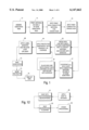
- FIG. 1 is a box diagram showing an exemplary method for producing RFID elements according to the present invention
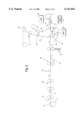
- FIG. 2 is a side schematic view of exemplary apparatus that may be used in the practice of the method as shown schematically in FIG. 1;
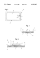
- FIG. 3 is a top plan view of one form of an exemplary RFID element according to the present invention.
- FIG. 4 is a side detail view, partly in cross-section and partly in elevation, of the element of FIG. 3 showing the interconnection between the chip and antenna;
- FIG. 5 is a view like that of FIG. 4 only showing another embodiment according to the present invention.
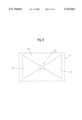
- FIG. 6 is a view like that of FIG. 3 only showing another embodiment of an RFID element according to the present invention.
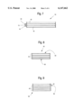
- FIGS. 7 through 9 are side schematic enlarged views of various forms of completed RFID elements according to the present invention, FIG. 8 showing the RFID element in the form of a linerless label and FIG. 9 showing the RFID element in the form of a linered label;
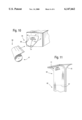
- FIG. 10 is a schematic perspective illustration of the application of a linerless label from a roll of labels like that of FIG. 8 to a package or other structure designed to have RFID technology associated therewith;
- FIG. 11 is a top perspective view showing a linered label such as illustrated in FIG. 3 with the release liner being separated therefrom, and interconnected to like elements;
- FIG. 12 is a box diagram showing a modification of the method of FIG. 1 at a particular area thereof.
- FIGS. 1 and 2 schematically illustrate the practice of various aspects of a method according to the present invention for producing an RFID element, such as any one of the elements illustrated in FIGS. 3 through 11.
- a flexible substantially dielectric base substrate web 10 (see FIG. 2) is unwound from a roll 11, as illustrated schematically by box 12 in FIG. 1.
- the web 10 preferably is paper of any desired conventional type and weight for producing the particular RFID element that will be produced, although a wide variety of other substrates may be utilized including a wide variety of different plastic substrates or--if flexible enough--cardboard, or the like. While the method steps, and the apparatus for the practice thereof, are illustrated in a particular sequence in FIGS. 1 and 2, it is to be understood that a number of the steps may be practiced in different order without adversely affecting the desired results according to the invention.
- Box 13 illustrated in FIG. 1 indicates the method procedure of printing the antenna on one face or side (in this case the top face of the web 10 illustrated in FIG. 2) of the base substrate web 10, for example utilizing conventional printing cylinders 14 (FIG. 2).
- the RFID antenna may be printed with any suitable conductive ink or toner, such as the water based conductive carbon ink, such as that sold by DuPont Electronic Materials with the trade designation E95817-152, or a water based silver ink sold by Acheson Colloids Company of Port Huron, Mich. with the product designation PE-001.
- the material for printing the antenna utilized in box 13, and with apparatus 14, may be an ink that includes resin and wax (typically a plurality of each), such as disclosed in U.S. Pat. No.
- thermoplastic resin and wax carrier is solid at ambient temperature, but becomes fluid at the operating temperature of the printer 14 (which may be a conventional pattern coater), and a relatively thick film (e.g. on the order of 3-15 microns) may be readily printed on the substrate 10 even with an operating speed of about 500 feet per minute or greater (that is the speed of the web 10), e.g. 500-1500 fpm.
- a non-conductive material is spot printed over a portion of the antenna for cross-over. This is illustrated schematically by box 16 in FIG. 1, and by the conventional printing equipment 17 in FIG. 2.
- the conductive material antenna 18 was printed at 13 but without a connection between the portions 19 and 20 thereof, and in box 16 the non-conductive material is printed on the face 22, over the antenna 18 at the area of the portions 19, 20 thereof.
- the face 22 is the first, top, face of the web 10 as seen in FIG. 2.
- the non-conductive material 21 for the cross-over may be any suitable non-conductive material that can be applied by conventional printing/coating techniques.
- it may be a barium titanate, such as sold by Tam with the product designation Tamtron X7R302H, or it may be an acrylated oligomer, such as sold by Ferco under the product designation UV2001.
- a conductive cross-over element is printed on the non-conductive material 21.
- the cross-over element is indicated by reference numeral 25 in the exemplary embodiment of FIG. 3.
- the apparatus of FIG. 2 may include conventional scanning equipment 26 to scan the web 10 to ensure alignment and registery of the components for future processing, and for that purpose any suitable conventional sense lines, marks, or the like may be applied to the web 10, or the scanner 26 may be of the type that will sense the portions of the antenna 18 which have been applied.
- spot adhesive such as hot melt pressure sensitive adhesive, or heat cured adhesive
- spot adhesive may be applied to the second face 27 (see FIG. 4) of the web 10, opposite the first face 22, utilizing equipment schematically illustrated at 28 in FIG. 2.
- Exemplary hot melt adhesives that may be provided are for example sold under the trademarks "Duro-Tak 4144" or “Duro-Tak 8686". Where low peel pressure sensitive adhesives are utilized, Nacor® 4536 water borne acrylic pressure sensitive adhesives may be utilized. The Duro-Tak and Nacor® products are sold by National Starch and Chemical Company.
- the adhesive 29 (see FIG. 4) so applied is adapted to receive a conventional RFID chip 30, having contacts 31 thereof.
- the contacts 31 may be of any suitable construction, and may be tapered to a point or to substantially a knife edge to facilitate penetration of the base substrate/web 10 as will be hereinafter described.
- a dryer or like apparatus 32 is provided after the spot adhesive applicator 28.
- the RFID chip 30 is brought into operative contact with the antenna 18 by pushing the chip 30 into operative contact with the base substrate 10 second face 27, and by pressing the chip contacts 31 through the base substrate 10 from the second face 27 thereof, into contact with the antenna 18 (including perhaps portion 20 thereof).
- the chip 30 is secured in place by the adhesive 29, and/or by mechanical locking with the substrate 27, or by applying a subsequent substrate or coating (which also may provide a protective function), or by a combination of these.
- FIG. 1 An alternative procedure, for production of the RFID element 36 of FIG. 5, is illustrated by boxes 37 and 38 in FIG. 1.
- a non-conductive material 40--like the material 21, for example--and which may or may not have the openings 41 therein is applied over the top face 22 of the substrate 10 over at least part of the antenna 18 and taking up an area significantly greater than the area of the chip 30 and contacts 31 thereof.
- the chip 30 is then moved into operative contact with the antenna 18 by passing the contacts 31 through the openings 41, or by penetrating the material 40 with the contacts 31 if "sharp".
- the chip 30 may be held to the material 40 by a conventional pressure sensitive or other adhesive 42, similar to the adhesive 29.
- the method further comprises--as illustrated schematically at box 44--applying protective substrates or coatings to one or both of the chip 30 and antenna 18.
- a protective substrate may be any conventional protective material, such as another sheet of paper, a foamed element, a plastic sheet having abrasion and/or cushioning properties, or the like. Where a substrate is provided preferably it is held in contact with the RFID element that exists at that stage with adhesive.
- FIG. 2 illustrates various equipment for providing protective substrates 45, 46 to both the faces 22, 27 of the base substrate 10 utilizing hot melt pressure sensitive adhesive which is applied as schematically illustrated at 47 and 48 in FIG. 2.
- the substrate 45 may be printed or otherwise imaged with indicia, as illustrated schematically at 50 in FIG. 2, e.g. to produce the indicia 51 illustrated in FIGS. 10 and 11, which will be described hereafter.
- FIG. 7 schematically illustrates the RFID element 15 which has the protective substrates 45, 46 in operative association therewith, held in place by the adhesive layers 53, 54 applied at the stations 47, 48 of FIG. 2, respectively.
- the final RFID element 55 (see FIG. 7) so produced may be a card, tag, or like structure. Alternatively, either a linerless or a lined label may be made from the structure 55.
- FIG. 8 illustrates schematically a linerless label 56 produced from the basic RFID element 55 of FIG. 7, the linerless label 56 also illustrated in FIG. 10 and shown as taken from a roll 57 therein.
- the apparatus of FIG. 2 for providing the linerless label includes a pressure sensitive adhesive applicator 58 which applies the adhesive 59 seen in FIGS. 8 and 10. For example a hot melt pressure sensitive adhesive 59 may be applied.
- the substrate 46 either inherently has the pressure sensitive adhesive release coat 60 (see FIGS. 2, 8, and 10) thereon, or the release coat 60 is applied as illustrated schematically by the apparatus 61 in FIG. 2.
- the roll of linerless labels 57 so produced may have perforations, die cuts, or like lines of weakness separating each element 56 from another.
- FIG. 8 shows the adhesive 66 applied by the station 63, and the release liner 65 in contact with the adhesive 66, while FIG. 11 shows the release liner 65 being pulled away from the rest of the RFID element 62.
- a line of weakness 67 such as introduced by the perf or die cut equipment schematically illustrated at 68 in FIG. 2.
- verification apparatus 70 is provided just before the take-up roll 71, and marking equipment 72 for bad units may be provided just downstream of the verification unit 70. These procedures are illustrated schematically at 73 and 74 in FIG. 1, while the take-up is illustrated schematically 75 therein. All of the equipment utilized in FIG. 2 is conventional equipment, no special equipment being necessary to practice the invention.
- a protective coating may be applied.
- a substrate such as the substrates 45, 46
- a protective coating may be applied.
- FIG. 12 One exemplary manner and construction for doing this is illustrated schematically in FIG. 12 wherein alter the box 80 where the chip 30 was applied to the antenna 18 (either in the manners illustrated in FIGS. 3 through 5, or in some other way) one or both faces 22, 27 of the substrate, including the elements 30 and/or 18 associated therewith, are coated with heat expandable microspheres, as illustrated schematically at 81, utilizing conventional technology, and conventional microspheres.
- the microspheres may be applied over the entire substrate face 22, 27, or just two selected areas thereof. Then--as illustrated schematically at 82 in FIG.
- FIG. 6 illustrates a different form of RFID element that may be produced according to the invention, having a different type of antenna.
- components comparable to those in the FIGS. 3 and 4 embodiments are shown by, the same reference numeral only preceded by a "1" .
- the antenna 118 is a bistatik antenna which is printed utilizing any of the conventional or suitable materials described above with respect to the antenna 18, and the chip--shown in dotted line because it is on the opposite side of the element 115 from the antenna 118--130 has the contacts thereof pressed into operative association with the antenna elements 118.
- the chip 130 may be held in place on the face opposite the face 122 (like the face 27) with an adhesive comparable to the adhesive 29 in the FIG. 4 embodiment.
- any suitable adhesive may be utilized as the adhesive 59, 66 for the label versions of the invention, including repositional and removable adhesives. Also different RFID elements aside from the cards and labels described may be produced, including other types of business forms such as mailer type business forms, tags for merchandise, or the like.
Abstract
Description
Claims (31)
Priority Applications (10)
| Application Number | Priority Date | Filing Date | Title |
|---|---|---|---|
| US09/393,291 US6147662A (en) | 1999-09-10 | 1999-09-10 | Radio frequency identification tags and labels |
| MXPA02002415A MXPA02002415A (en) | 1999-09-10 | 2000-09-07 | Adio frequency identification tags and labels. |
| JP2001522489A JP2003509750A (en) | 1999-09-10 | 2000-09-07 | Radio frequency identification tags and labels |
| AU71184/00A AU772878B2 (en) | 1999-09-10 | 2000-09-07 | Radio frequency identification tags and labels |
| ARP000104677A AR025586A1 (en) | 1999-09-10 | 2000-09-07 | RADIO FREQUENT IDENTIFIER ELEMENT AND METHOD TO PRODUCE IT |
| CA002384649A CA2384649C (en) | 1999-09-10 | 2000-09-07 | Radio frequency identification tags and labels |
| EP00959954A EP1222622A2 (en) | 1999-09-10 | 2000-09-07 | Radio frequency identification tags and labels |
| BR0013918-1A BR0013918A (en) | 1999-09-10 | 2000-09-07 | Radio frequency identification tags and labels |
| PCT/US2000/024474 WO2001018749A2 (en) | 1999-09-10 | 2000-09-07 | Radio frequency identification tags and labels |
| HK02106746.2A HK1047491A1 (en) | 1999-09-10 | 2002-09-13 | Radio frequency identification tags and labels |
Applications Claiming Priority (1)
| Application Number | Priority Date | Filing Date | Title |
|---|---|---|---|
| US09/393,291 US6147662A (en) | 1999-09-10 | 1999-09-10 | Radio frequency identification tags and labels |
Publications (1)
| Publication Number | Publication Date |
|---|---|
| US6147662A true US6147662A (en) | 2000-11-14 |
Family
ID=23554098
Family Applications (1)
| Application Number | Title | Priority Date | Filing Date |
|---|---|---|---|
| US09/393,291 Expired - Lifetime US6147662A (en) | 1999-09-10 | 1999-09-10 | Radio frequency identification tags and labels |
Country Status (10)
| Country | Link |
|---|---|
| US (1) | US6147662A (en) |
| EP (1) | EP1222622A2 (en) |
| JP (1) | JP2003509750A (en) |
| AR (1) | AR025586A1 (en) |
| AU (1) | AU772878B2 (en) |
| BR (1) | BR0013918A (en) |
| CA (1) | CA2384649C (en) |
| HK (1) | HK1047491A1 (en) |
| MX (1) | MXPA02002415A (en) |
| WO (1) | WO2001018749A2 (en) |
Cited By (176)
| Publication number | Priority date | Publication date | Assignee | Title |
|---|---|---|---|---|
| WO2001071848A1 (en) * | 2000-03-21 | 2001-09-27 | Mikoh Corporation | A tamper indicating radio frequency identification label |
| US20010027401A1 (en) * | 1999-05-31 | 2001-10-04 | Elliot Klein | Product warranty registration system and method |
| US20010037248A1 (en) * | 2000-05-01 | 2001-11-01 | Elliot Klein | Product warranty registration system and method |
| FR2817373A1 (en) * | 2000-11-30 | 2002-05-31 | D Vito Antoine Orazio | Production of portable objects such as electronic labels using flexography or other rotating printing processes so that the production process can be increasingly automated and production rates increased |
| US6424315B1 (en) * | 2000-08-02 | 2002-07-23 | Amkor Technology, Inc. | Semiconductor chip having a radio-frequency identification transceiver |
| US6451154B1 (en) * | 2000-02-18 | 2002-09-17 | Moore North America, Inc. | RFID manufacturing concepts |
| US20020147042A1 (en) * | 2001-02-14 | 2002-10-10 | Vt Tech Corp. | System and method for detecting the result of a game of chance |
| WO2002099764A1 (en) * | 2001-06-05 | 2002-12-12 | Motorola, Inc. | Capacitively powered data communication system with tag and circuit carrier apparatus for use therein |
| US20020189667A1 (en) * | 2001-06-13 | 2002-12-19 | O'dougherty Kevin T. | Liquid handling system with electronic information storage |
| US6518887B2 (en) * | 2000-03-09 | 2003-02-11 | Sony Chemicals Corp. | Information recording tag |
| WO2003017191A2 (en) * | 2001-08-15 | 2003-02-27 | Moore North America, Inc. | Rfid tag having integral electrical bridge and method of assembling the same |
| EP1302895A2 (en) * | 2001-10-09 | 2003-04-16 | Sonoco Development, Inc. | Conductive electrical element and antenna with ink additive technology |
| US20030087072A1 (en) * | 2001-11-07 | 2003-05-08 | Huffer Scott W | EB pattern profile printing |
| US6569508B2 (en) | 1999-01-13 | 2003-05-27 | Brady Worldwide, Inc. | Label having a protective cavity and method of manufacture |
| EP1233426A3 (en) * | 2001-02-15 | 2003-07-09 | Integral Technologies, Inc. | Antennas with conductive plastics or conductive composites |
| US20030145945A1 (en) * | 2002-02-06 | 2003-08-07 | Kennedy Patrick R. | Labeling assembly |
| WO2003071476A1 (en) * | 2002-02-19 | 2003-08-28 | Koninklijke Philips Electronics N.V. | Method of manufacturing a transponder |
| US6634560B1 (en) * | 1999-12-14 | 2003-10-21 | Moore North America, Inc. | Radio frequency identification tagging, encoding/reading through a digitizer tablet |
| US6649829B2 (en) | 2001-05-21 | 2003-11-18 | Colder Products Company | Connector apparatus and method for connecting the same for controlling fluid dispensing |
| US6660557B2 (en) * | 2000-03-28 | 2003-12-09 | Hitachi, Ltd. | Method of manufacturing an electronic device |
| EP1375131A1 (en) * | 2002-06-28 | 2004-01-02 | Infineon Technologies AG | Laminat comprising an electrically conducting layer as antenna |
| US20040005178A1 (en) * | 2000-06-23 | 2004-01-08 | Georg Frohlich | Device and method for a printing and/or copying device with reduced thermal stress on the support material |
| US20040020040A1 (en) * | 2002-08-02 | 2004-02-05 | Matrics, Inc. | Method and system for forming a die frame for transferring dies therewith |
| US20040020036A1 (en) * | 2002-08-02 | 2004-02-05 | Matrics, Inc. | Method and apparatus for high volume assembly of radio frequency identification tags |
| US20040051666A1 (en) * | 2001-02-16 | 2004-03-18 | Integral Technologies, Inc. | Low cost antennas using conductive plastics or conductive composites |
| US6741212B2 (en) | 2001-09-14 | 2004-05-25 | Skycross, Inc. | Low profile dielectrically loaded meanderline antenna |
| EP1425713A1 (en) * | 2001-07-04 | 2004-06-09 | Rafsec OY | An injection moulded product and a method for its manufacture |
| US20040122777A1 (en) * | 2002-12-18 | 2004-06-24 | Pitney Bowes Incorporated | Dual metering method for enhanced mail security |
| US20040134620A1 (en) * | 2000-10-23 | 2004-07-15 | Soeborg Jens La Cour | Printer for preparing at least labels as destination information carriers for an article to be transported and a tag, a system and a method thereof |
| EP1444099A2 (en) * | 2001-10-01 | 2004-08-11 | ZIH Corp. | Method and apparatus for associating on demand certain selected media and value-adding elements |
| US20040154161A1 (en) * | 2003-02-07 | 2004-08-12 | Hallys Corporation | Random-period chip transfer apparatus |
| US20040172160A1 (en) * | 2001-06-13 | 2004-09-02 | O'dougherty Kevin T. | Secure reader system |
| US20040169586A1 (en) * | 2001-05-31 | 2004-09-02 | Rafsac Oy | Smart label and a smart label web |
| US6816380B2 (en) | 2001-05-31 | 2004-11-09 | Alien Technology Corporation | Electronic devices with small functional elements supported on a carrier |
| US20040233189A1 (en) * | 1997-11-13 | 2004-11-25 | Kozo Masuda | Display unit |
| US20040238623A1 (en) * | 2003-05-09 | 2004-12-02 | Wayne Asp | Component handling device having a film insert molded RFID tag |
| FR2855637A1 (en) * | 2003-05-26 | 2004-12-03 | A S K | METHOD FOR MANUFACTURING A CONTACTLESS TICKET AND TICKET OBTAINED THEREFROM |
| US20040251541A1 (en) * | 2003-06-12 | 2004-12-16 | Matrics, Inc. | Method, system, and apparatus for high volume assembly of compact discs and volume assembly of compact discs and digital video discs incorporating radio frequency identification tag technology |
| US6842148B2 (en) | 2001-04-16 | 2005-01-11 | Skycross, Inc. | Fabrication method and apparatus for antenna structures in wireless communications devices |
| US20050007290A1 (en) * | 2001-02-15 | 2005-01-13 | Integral Technologies, Inc. | Low cost omni-directional antenna manufactured from conductive loaded resin-based materials |
| US20050012616A1 (en) * | 2003-07-07 | 2005-01-20 | Forster Ian J. | RFID device with changeable characteristics |
| US20050024287A1 (en) * | 2003-05-29 | 2005-02-03 | Young-Min Jo | Radio frequency identification tag |
| US20050078050A1 (en) * | 2001-02-15 | 2005-04-14 | Integral Technologies, Inc. | Low cost antenna devices comprising conductive loaded resin-based materials with conductive wrapping |
| US20050087607A1 (en) * | 2001-12-21 | 2005-04-28 | Samuli Stromberg | Smart label web and a method for its manufacture |
| US20050091821A1 (en) * | 2003-11-03 | 2005-05-05 | Best Scott D. | Method of manufacturing an article having a radio frequency identification (RFID) device |
| US20050139667A1 (en) * | 2003-09-12 | 2005-06-30 | Barrus Gordon B. | RFID tag, antenna, and printer system |
| US20050151699A1 (en) * | 2004-01-12 | 2005-07-14 | Symbol Technologies, Inc. | Method and system for manufacturing radio frequency identification tag antennas |
| US20050155213A1 (en) * | 2004-01-12 | 2005-07-21 | Symbol Technologies, Inc. | Radio frequency identification tag inlay sortation and assembly |
| WO2005078648A1 (en) * | 2004-02-13 | 2005-08-25 | Man Roland Druckmaschinen Ag | Method for producing rfid labels |
| US20050199724A1 (en) * | 2004-03-01 | 2005-09-15 | Allen Lubow | Diffractive optical variable image including barcode |
| US20050200041A1 (en) * | 2001-02-15 | 2005-09-15 | Integral Technologies, Inc. | Low cost hardware manufactured from conductive loaded resin-based materials |
| US20050204544A1 (en) * | 2001-02-15 | 2005-09-22 | Integral Technologies, Inc. | Low cost electrical motor components manufactured from conductive loaded resin-based materials |
| US20050206028A1 (en) * | 2001-02-15 | 2005-09-22 | Integral Technologies, Inc. | Low cost electrically conductive flooring tile manufactured from conductive loaded resin-based materials |
| US20050212161A1 (en) * | 2001-02-15 | 2005-09-29 | Integral Technologies, Inc. | Low cost conductive pipe manufactured from conductive loaded resin-based materials |
| US6951596B2 (en) | 2002-01-18 | 2005-10-04 | Avery Dennison Corporation | RFID label technique |
| US20050224590A1 (en) * | 2004-04-13 | 2005-10-13 | John Melngailis | Method and system for fabricating integrated circuit chips with unique identification numbers |
| US20050230867A1 (en) * | 2001-02-15 | 2005-10-20 | Integral Technologies, Inc. | Low cost vehicle electrical and electronic components and systems manufactured from conductive loaded resin-based materials |
| US20050241506A1 (en) * | 2004-05-03 | 2005-11-03 | Man Roland Druckmaschinen Ag | Method for printing an electronic circuit component on a substrate using a printing machine |
| US20050241146A1 (en) * | 2004-04-30 | 2005-11-03 | William Hamburgen | Method of fabricating a rat's nest RFID antenna |
| US20050247782A1 (en) * | 2004-04-23 | 2005-11-10 | Gougen Ambartsoumian | Low temperature radio frequency identification tracking system |
| US20050273434A1 (en) * | 2004-04-18 | 2005-12-08 | Allen Lubow | System and method for managing security in a supply chain |
| WO2005119617A1 (en) * | 2004-06-01 | 2005-12-15 | Filtrona United Kingdom Limited | Improvements in or relating to article tagging |
| US20050284917A1 (en) * | 2004-06-24 | 2005-12-29 | Checkpoint Systems, Inc. | Die attach area cut-on-fly method and apparatus |
| US20050284941A1 (en) * | 2004-06-28 | 2005-12-29 | Allen Lubow | Combined electromagnetic and optical communication system |
| US20060012387A1 (en) * | 2004-06-29 | 2006-01-19 | Symbol Technologies, Inc. | Systems and methods for testing radio frequency identification tags |
| US20060038687A1 (en) * | 2004-08-17 | 2006-02-23 | Symbol Technologies, Inc. | Singulation of radio frequency identification (RFID) tags for testing and/or programming |
| US20060043196A1 (en) * | 2004-08-27 | 2006-03-02 | Goodyear Tire And Rubber Company | Air spring mount assembly with identification tag |
| US20060071084A1 (en) * | 2000-12-15 | 2006-04-06 | Electrox Corporation | Process for manufacture of novel, inexpensive radio frequency identification devices |
| FR2876507A1 (en) * | 2004-10-12 | 2006-04-14 | K Sa As | CONTACTLESS LABEL WITH AN OMNIDIRECTIONAL Y-ANTENNA |
| US20060086807A1 (en) * | 2004-10-25 | 2006-04-27 | Lexmark International, Inc. | Deposition fabrication using inkjet technology |
| US20060128895A1 (en) * | 2001-02-15 | 2006-06-15 | Thomas Aisenbrey | Electriplast thermoset wet mix material and method of manufacture |
| EP1689020A1 (en) * | 2005-01-28 | 2006-08-09 | Nordenia Deutschland Gronau GmbH | Foil with a printed antenna |
| US20060186204A1 (en) * | 2004-06-28 | 2006-08-24 | International Barcode Corporation | Combined multi-frequency electromagnetic and optical communication system |
| US20060196936A1 (en) * | 2005-01-06 | 2006-09-07 | Quad/Graphics, Inc. | Resonator use in the print field |
| US20060205113A1 (en) * | 2005-03-14 | 2006-09-14 | Rcd Technology Corp. | Radio frequency identification (RFID) tag lamination process |
| US20060205115A1 (en) * | 2005-03-14 | 2006-09-14 | Rcd Technology Corp. | Radio frequency identification (RFID) tag lamination process using liner |
| EP1703589A1 (en) * | 2005-03-17 | 2006-09-20 | Fujitsu Ltd. | Tag antenna |
| US20060223225A1 (en) * | 2005-03-29 | 2006-10-05 | Symbol Technologies, Inc. | Method, system, and apparatus for transfer of integrated circuit dies using an attractive force |
| US20060232589A1 (en) * | 2005-04-19 | 2006-10-19 | Microsoft Corporation | Uninterrupted execution of active animation sequences in orphaned rendering objects |
| US20060248767A1 (en) * | 2005-04-28 | 2006-11-09 | Zih Corp. | Antimicrobial coating for identification devices |
| US20060261957A1 (en) * | 2003-08-26 | 2006-11-23 | Ralf God | Method for producing bridge modules |
| US20060267200A1 (en) * | 2005-05-13 | 2006-11-30 | University Of Pittsburgh - Of The Commonwealth System Of Higher Education | Method of making an electronic device using an electrically conductive polymer, and associated products |
| US20060283932A1 (en) * | 2005-04-08 | 2006-12-21 | Wayne Asp | Identification tag for fluid containment drum |
| US7154283B1 (en) | 2006-02-22 | 2006-12-26 | Avery Dennison Corporation | Method of determining performance of RFID devices |
| US7159298B2 (en) * | 2001-03-15 | 2007-01-09 | Daniel Lieberman | Method for the formation of RF antennas by demetallizing |
| EP1742171A1 (en) * | 2004-04-27 | 2007-01-10 | Dainippon Printing Co., Ltd. | Method for manufacturing sheet provided with ic tag, apparatus for manufacturing sheet provided with ic tag, sheet provided with ic tag, method for fixing ic chip, apparatus for fixing ic chip, and ic tag |
| US20070007661A1 (en) * | 2005-06-09 | 2007-01-11 | Burgess Lester E | Hybrid conductive coating method for electrical bridging connection of RFID die chip to composite antenna |
| US20070012773A1 (en) * | 2005-06-07 | 2007-01-18 | University Of Pittsburgh - Of The Commonwealth System Of Higher Education | Method of making an electronic device using an electrically conductive polymer, and associated products |
| US20070031992A1 (en) * | 2005-08-05 | 2007-02-08 | Schatz Kenneth D | Apparatuses and methods facilitating functional block deposition |
| US20070039694A1 (en) * | 2003-08-01 | 2007-02-22 | Thomas Walther | Method for producing rfid labels |
| US20070085069A1 (en) * | 2003-12-26 | 2007-04-19 | Shinko Electric Co., Ltd. | Method and apparatus for manufacturing ic chip packaged device |
| US7214569B2 (en) | 2002-01-23 | 2007-05-08 | Alien Technology Corporation | Apparatus incorporating small-feature-size and large-feature-size components and method for making same |
| US20070115645A1 (en) * | 2001-08-17 | 2007-05-24 | Jacobsen Jeffrey J | Apparatuses and methods for forming wireless RF labels |
| US20070113966A1 (en) * | 2004-02-23 | 2007-05-24 | Checkpoint Systems, Inc. | Process for forming at least a portion of a package or an envelope bearing a printed indicia |
| US20070131769A1 (en) * | 2004-08-12 | 2007-06-14 | Brother Kogyo Kabushiki Kaisha | Label Producing Apparatus |
| US20070131016A1 (en) * | 2005-12-13 | 2007-06-14 | Symbol Technologies, Inc. | Transferring die(s) from an intermediate surface to a substrate |
| US20070131781A1 (en) * | 2005-12-08 | 2007-06-14 | Ncr Corporation | Radio frequency device |
| US20070139057A1 (en) * | 2005-12-15 | 2007-06-21 | Symbol Technologies, Inc. | System and method for radio frequency identification tag direct connection test |
| US7236093B2 (en) | 2000-01-17 | 2007-06-26 | Upm Raflatac Oy | Method for the manufacture of a smart label inlet web, and a smart label inlet web |
| US20070146143A1 (en) * | 2005-12-22 | 2007-06-28 | Checkpoint Systems, Inc. | Smart corrugated cardboard |
| US20070144662A1 (en) * | 2005-12-22 | 2007-06-28 | Armijo Edward A | Method of manufacturing RFID devices |
| US20070158024A1 (en) * | 2006-01-11 | 2007-07-12 | Symbol Technologies, Inc. | Methods and systems for removing multiple die(s) from a surface |
| US7244332B2 (en) | 2000-12-11 | 2007-07-17 | Rafsec Oy | Smart label web and a method for its manufacture |
| US20070171129A1 (en) * | 2006-01-24 | 2007-07-26 | Avery Dennison Corporation | Radio frequency (RF) antenna containing element and methods of making the same |
| US7253735B2 (en) | 2003-03-24 | 2007-08-07 | Alien Technology Corporation | RFID tags and processes for producing RFID tags |
| US20070188332A1 (en) * | 2005-10-18 | 2007-08-16 | Peter Phaneuf | Label with electronic components and method of making same |
| GB2436164A (en) * | 2006-03-16 | 2007-09-19 | Uvasol Ltd | Improvements in electrical connections between electronic components and conductive tracks |
| US20070222615A1 (en) * | 2006-03-24 | 2007-09-27 | Koshiro Yamaguchi | RFID label with increased readability of printed images |
| US20070230103A1 (en) * | 2006-04-04 | 2007-10-04 | Man Roland Druckmaschinen Ag | Application of electronic components in printed products |
| US20070244657A1 (en) * | 2006-04-11 | 2007-10-18 | Drago Randall A | Methods and systems for testing radio frequency identification (RFID) tags having multiple antennas |
| US7288432B2 (en) | 1999-03-16 | 2007-10-30 | Alien Technology Corporation | Electronic devices with small functional elements supported on a carrier |
| WO2007143527A2 (en) * | 2006-06-01 | 2007-12-13 | S.D. Warren Company | Rfid tags and antennas and methods of their manufacture |
| US20080040913A1 (en) * | 2005-03-22 | 2008-02-21 | Fujitsu Limited | RFID tag |
| EP1892650A1 (en) * | 2006-08-26 | 2008-02-27 | Nordenia Deutschland Gronau GmbH | Method for contactless testing of an antenna mounted on a sheet of material |
| US20080047660A1 (en) * | 2006-08-08 | 2008-02-28 | Ws Packaging Group, Inc. | Peel plate assembly for removing programmable transponders from a web |
| US20080063864A1 (en) * | 2001-02-15 | 2008-03-13 | Thomas Aisenbrey | Variable-thickness elecriplast moldable capsule and method of manufacture |
| US7353598B2 (en) | 2004-11-08 | 2008-04-08 | Alien Technology Corporation | Assembly comprising functional devices and method of making same |
| US20080088448A1 (en) * | 2006-06-30 | 2008-04-17 | Steidinger David J | Method of making an rfid article |
| US20080129455A1 (en) * | 2006-05-24 | 2008-06-05 | Rcd Technology Inc. | Method for forming rfid tags |
| US7385284B2 (en) | 2004-11-22 | 2008-06-10 | Alien Technology Corporation | Transponder incorporated into an electronic device |
| US20080150719A1 (en) * | 2006-12-20 | 2008-06-26 | Checkpoint Systems, Inc. | Eas and uhf combination tag |
| US20080150732A1 (en) * | 2006-12-22 | 2008-06-26 | Vigilan, Incorporated | Sensors and systems for detecting environmental conditions or changes |
| US20080156446A1 (en) * | 2006-12-28 | 2008-07-03 | Ricoh Company, Ltd | Conveyance system having identification attaching unit |
| US7452748B1 (en) | 2004-11-08 | 2008-11-18 | Alien Technology Corporation | Strap assembly comprising functional block deposited therein and method of making same |
| US20080286506A1 (en) * | 2007-05-16 | 2008-11-20 | Mpt, Inc. | In-mold labeling system for containers |
| US7500307B2 (en) | 2004-09-22 | 2009-03-10 | Avery Dennison Corporation | High-speed RFID circuit placement method |
| US7542301B1 (en) | 2005-06-22 | 2009-06-02 | Alien Technology Corporation | Creating recessed regions in a substrate and assemblies having such recessed regions |
| US7551141B1 (en) | 2004-11-08 | 2009-06-23 | Alien Technology Corporation | RFID strap capacitively coupled and method of making same |
| US20090206012A1 (en) * | 2006-06-23 | 2009-08-20 | Tim Wirsching | Sorting device and method for sorting rfid tags |
| US20090231139A1 (en) * | 2006-05-12 | 2009-09-17 | All-Tag Security S.A. | Label Incorporating an RF Anti-Theft Antenna and a UHF RFID Transponder |
| US7623034B2 (en) | 2005-04-25 | 2009-11-24 | Avery Dennison Corporation | High-speed RFID circuit placement method and device |
| US7661591B2 (en) | 2000-10-20 | 2010-02-16 | Promega Corporation | RF point of sale and delivery method and system using communication with remote computer and having features to read a large number of RF tags |
| US7688206B2 (en) | 2004-11-22 | 2010-03-30 | Alien Technology Corporation | Radio frequency identification (RFID) tag for an item having a conductive layer included or attached |
| WO2010040399A1 (en) * | 2008-10-08 | 2010-04-15 | Laird Technologies Ab | Method for protecting a condutive material structure provided on a carrier |
| US7710275B2 (en) | 2007-03-16 | 2010-05-04 | Promega Corporation | RFID reader enclosure and man-o-war RFID reader system |
| USRE41361E1 (en) * | 2001-04-25 | 2010-06-01 | Muhlbauer Ag | Method for connecting microchips to an antenna arranged on a support strip for producing a transponder |
| US7735732B2 (en) | 2000-10-20 | 2010-06-15 | Promega Corporation | Radio frequency identification method and system of distributing products |
| US20100192361A1 (en) * | 2001-02-15 | 2010-08-05 | Integral Technologies, Inc. | Low cost electrical terminals manufactured from conductive loaded resin-based materials |
| US20100283499A1 (en) * | 2009-05-08 | 2010-11-11 | Robert Addison Bourdreau | Non-contact testing of printed electronics |
| US20100326236A1 (en) * | 2001-02-15 | 2010-12-30 | Integral Technologies, Inc. | Low cost housings for vehicle mechanical devices and systems manufactured from conductive loaded resin-based materials |
| US20110024275A1 (en) * | 2001-02-16 | 2011-02-03 | Integral Technologies, Inc. | Low cost key actuators and other switching device actuators manufactured from conductive loaded resin-based materials |
| US7948384B1 (en) * | 2007-08-14 | 2011-05-24 | Mpt, Inc. | Placard having embedded RFID device for tracking objects |
| US20110211975A1 (en) * | 2010-02-26 | 2011-09-01 | Entegris, Inc. | Method and system for controlling operation of a pump based on filter information in a filter information tag |
| US20110211976A1 (en) * | 2010-02-26 | 2011-09-01 | Entegris, Inc. | Method and system for optimizing operation of a pump |
| US20110256357A1 (en) * | 2010-04-14 | 2011-10-20 | Avery Dennison Corporation | Method of Assembly of Articles and Intermediate Created Thereby |
| EP2482237A1 (en) | 2011-01-26 | 2012-08-01 | Nordenia Technologies GmbH | Body in the form of a packaging or a moulded part comprising an RFID-Antenna |
| US8248246B2 (en) | 2003-11-25 | 2012-08-21 | Brother Kogyo Kabushiki Kaisha | RFID-tag fabricating apparatus and cartridge |
| US20120280047A1 (en) * | 2010-06-14 | 2012-11-08 | Avery Dennison Corporation | Method, System and Apparatus for Making Short Run Radio Frequency Identification Tags and Labels |
| US8313594B2 (en) | 2000-01-24 | 2012-11-20 | Nextreme, Llc | Method and apparatus for thermoplastic sheet with RFID |
| CN101877072B (en) * | 2009-04-28 | 2013-02-13 | 吴军华 | Manufacturing method and system of radio frequency self-adhesive label |
| US20130068511A1 (en) * | 2011-09-19 | 2013-03-21 | Xerox Corporation | System and method for formation of electrical conductors on a substrate |
| US8502684B2 (en) | 2006-12-22 | 2013-08-06 | Geoffrey J. Bunza | Sensors and systems for detecting environmental conditions or changes |
| US8580338B1 (en) * | 2006-12-19 | 2013-11-12 | Polymeric LLC | Embossed durable supports with RFID chip, for labeling and relabeling objects |
| US8665071B2 (en) | 2004-03-19 | 2014-03-04 | Applied Biosystems, Llc | Methods and systems for using RFID in biological field |
| US8753097B2 (en) | 2005-11-21 | 2014-06-17 | Entegris, Inc. | Method and system for high viscosity pump |
| US8866595B1 (en) * | 2010-09-25 | 2014-10-21 | Impinj, Inc. | Ticket-based RFID loss-prevention system |
| US8931166B2 (en) | 2011-05-19 | 2015-01-13 | Tecnomar Oy | Manufacturing method of electrical bridges suitable for reel to reel mass manufacturing |
| US9031683B2 (en) | 2006-07-10 | 2015-05-12 | Entegris, Inc. | Systems and methods for managing material storage vessels having information storage elements |
| US9090399B2 (en) * | 2009-04-03 | 2015-07-28 | Maricap Oy | Method and means in waste handling |
| US9230227B2 (en) | 2000-01-24 | 2016-01-05 | Nextreme, Llc | Pallet |
| US9297374B2 (en) | 2010-10-20 | 2016-03-29 | Entegris, Inc. | Method and system for pump priming |
| ITUB20154206A1 (en) * | 2015-10-07 | 2017-04-07 | Mecstar S R L | APPARATUS, METHOD AND DEVICE FOR THE REALIZATION OF INCORPORATING PRODUCTS A RFid |
| US9688058B2 (en) | 2015-01-30 | 2017-06-27 | R.R. Donnelley & Sons Company | Methods and apparatus for supporting radio frequency identification tags |
| US9691243B1 (en) | 2013-08-21 | 2017-06-27 | Impinj, Inc. | Exit-code-based RFID loss-prevention system |
| US20180101759A1 (en) * | 2016-10-07 | 2018-04-12 | Avery Dennison Retail Information Services, Llc | Vibratory feeder systems for rfid elements |
| IT201700001509A1 (en) * | 2017-01-09 | 2018-07-09 | Automation 4 Industiral Solutions S R L | METHOD AND PLANT FOR REALIZING RFID DEVICES |
| US20180350274A1 (en) * | 2017-05-30 | 2018-12-06 | Dongguan Morganprintone SmartTech Co.,Ltd. | Multi-functional, intelligent and eco-friendly tape |
| WO2019152563A1 (en) | 2018-01-30 | 2019-08-08 | Life Technologies Corporation | Instruments, devices and consumables for use in a workflow of a smart molecular analysis system |
| USRE47599E1 (en) | 2000-10-20 | 2019-09-10 | Promega Corporation | RF point of sale and delivery method and system using communication with remote computer and having features to read a large number of RF tags |
| US10455705B2 (en) | 2015-10-07 | 2019-10-22 | Mecstar S.R.L. | Apparatus, method and device for making products incorporating an RFid |
| US10470809B1 (en) | 2018-06-19 | 2019-11-12 | Summate Technologies, Inc. | Automated screw identification system and method |
| US10671969B2 (en) | 2017-05-03 | 2020-06-02 | Summate Technologies, Inc. | Operating room situated, parts-inventory control system and supervisory arrangement for accurately tracking the use of and accounting for the ultimate disposition of an individual component part of a complete implant which is then being surgically engrafted in-vivo upon or into the body of a living subject |
| CN111260014A (en) * | 2018-11-30 | 2020-06-09 | 恩旭有限公司 | Miniaturized radio frequency identification tag |
| WO2020160335A1 (en) | 2019-01-30 | 2020-08-06 | Life Technologies Holdings Pte Limited | Biological analysis system and methods |
| US10909343B1 (en) | 2019-07-12 | 2021-02-02 | Summate Technologies, Inc. | Automated screw identification system and method with labeled pegs |
| WO2021224892A1 (en) | 2020-05-08 | 2021-11-11 | Life Technologies Holdings Pte Limited | Biological analysis systems and methods |
Families Citing this family (9)
| Publication number | Priority date | Publication date | Assignee | Title |
|---|---|---|---|---|
| EP1699637B2 (en) † | 2003-08-01 | 2017-12-27 | manroland web systems GmbH | Method for further printing with electrical conductivity |
| JP4513052B2 (en) * | 2003-10-24 | 2010-07-28 | ブラザー工業株式会社 | Wireless tag information communication device |
| DE102004011702B4 (en) * | 2004-03-10 | 2006-02-16 | Circle Smart Card Ag | Method for producing a card body for a contactless chip card |
| ITMO20040080A1 (en) * | 2004-04-08 | 2004-07-08 | Windinglab S R L | METHOD OF CREATION OF A THIN THICK PRINTED CIRCUIT AND RELATED CIRCUIT |
| JP4677268B2 (en) * | 2005-04-08 | 2011-04-27 | トッパン・フォームズ株式会社 | RF-ID media inspection device |
| DE102005058101B4 (en) * | 2005-12-05 | 2019-04-25 | Smartrac Ip B.V. | Chip card and method for producing a chip card |
| KR101351904B1 (en) | 2006-04-28 | 2014-01-23 | 아스크 에세.아. | Radio frequency identification device support and its manufacturing method |
| KR101317633B1 (en) * | 2012-05-03 | 2013-10-10 | 한국과학기술원 | Rfid tag utilizing organic solar cells |
| MX359464B (en) * | 2012-11-13 | 2018-09-28 | Cooper Tire & Rubber Co | Product such as a tire with rfid tag with rubber, elastomer, or polymer antenna. |
Citations (25)
| Publication number | Priority date | Publication date | Assignee | Title |
|---|---|---|---|---|
| US4706050A (en) * | 1984-09-22 | 1987-11-10 | Smiths Industries Public Limited Company | Microstrip devices |
| US4783646A (en) * | 1986-03-07 | 1988-11-08 | Kabushiki Kaisha Toshiba | Stolen article detection tag sheet, and method for manufacturing the same |
| US5420757A (en) * | 1993-02-11 | 1995-05-30 | Indala Corporation | Method of producing a radio frequency transponder with a molded environmentally sealed package |
| US5444223A (en) * | 1994-01-11 | 1995-08-22 | Blama; Michael J. | Radio frequency identification tag and method |
| US5497140A (en) * | 1992-08-12 | 1996-03-05 | Micron Technology, Inc. | Electrically powered postage stamp or mailing or shipping label operative with radio frequency (RF) communication |
| US5528222A (en) * | 1994-09-09 | 1996-06-18 | International Business Machines Corporation | Radio frequency circuit and memory in thin flexible package |
| US5566441A (en) * | 1993-03-11 | 1996-10-22 | British Technology Group Limited | Attaching an electronic circuit to a substrate |
| US5574470A (en) * | 1994-09-30 | 1996-11-12 | Palomar Technologies Corporation | Radio frequency identification transponder apparatus and method |
| US5612513A (en) * | 1995-09-19 | 1997-03-18 | Micron Communications, Inc. | Article and method of manufacturing an enclosed electrical circuit using an encapsulant |
| US5660663A (en) * | 1994-05-10 | 1997-08-26 | Esselte Meto International Gmbh | Marking tag |
| GB2310977A (en) * | 1996-03-07 | 1997-09-10 | Jarvis Porter Group Plc | Flexible label containing detectable sensor for security tagging |
| US5682143A (en) * | 1994-09-09 | 1997-10-28 | International Business Machines Corporation | Radio frequency identification tag |
| US5708419A (en) * | 1996-07-22 | 1998-01-13 | Checkpoint Systems, Inc. | Method of wire bonding an integrated circuit to an ultraflexible substrate |
| US5719586A (en) * | 1992-05-15 | 1998-02-17 | Micron Communications, Inc. | Spherical antenna pattern(s) from antenna(s) arranged in a two-dimensional plane for use in RFID tags and labels |
| US5758575A (en) * | 1995-06-07 | 1998-06-02 | Bemis Company Inc. | Apparatus for printing an electrical circuit component with print cells in liquid communication |
| US5768217A (en) * | 1996-05-14 | 1998-06-16 | Casio Computer Co., Ltd. | Antennas and their making methods and electronic devices or timepieces with the antennas |
| US5776278A (en) * | 1992-06-17 | 1998-07-07 | Micron Communications, Inc. | Method of manufacturing an enclosed transceiver |
| US5779839A (en) * | 1992-06-17 | 1998-07-14 | Micron Communications, Inc. | Method of manufacturing an enclosed transceiver |
| US5817207A (en) * | 1995-10-17 | 1998-10-06 | Leighton; Keith R. | Radio frequency identification card and hot lamination process for the manufacture of radio frequency identification cards |
| US5838253A (en) * | 1995-05-17 | 1998-11-17 | Accu-Sort Systems, Inc. | Radio frequency identification label |
| US5867102A (en) * | 1997-02-27 | 1999-02-02 | Wallace Computer Services, Inc. | Electronic article surveillance label assembly and method of manufacture |
| US5973600A (en) * | 1997-09-11 | 1999-10-26 | Precision Dynamics Corporation | Laminated radio frequency identification device |
| US6024285A (en) * | 1997-08-19 | 2000-02-15 | Micron Technology, Inc. | Wireless communication devices and methods of forming wireless communication devices |
| US6037879A (en) * | 1997-10-02 | 2000-03-14 | Micron Technology, Inc. | Wireless identification device, RFID device, and method of manufacturing wireless identification device |
| US6045652A (en) * | 1992-06-17 | 2000-04-04 | Micron Communications, Inc. | Method of manufacturing an enclosed transceiver |
Family Cites Families (11)
| Publication number | Priority date | Publication date | Assignee | Title |
|---|---|---|---|---|
| AU626013B2 (en) * | 1988-07-04 | 1992-07-23 | Sony Corporation | A thin electronic device having an integrated circuit chip and a power battery and a method for producing same |
| GB9222460D0 (en) * | 1992-10-26 | 1992-12-09 | Hughes Microelectronics Europa | Radio frequency baggage tag |
| US5495250A (en) * | 1993-11-01 | 1996-02-27 | Motorola, Inc. | Battery-powered RF tags and apparatus for manufacturing the same |
| US5541399A (en) * | 1994-09-30 | 1996-07-30 | Palomar Technologies Corporation | RF transponder with resonant crossover antenna coil |
| DE4440721A1 (en) * | 1994-11-15 | 1996-05-23 | Datacolor Druck Und Fullservic | Carrier element for integrated circuit components in e.g. cheque and credit cards |
| DE19511300A1 (en) * | 1995-03-28 | 1996-10-02 | Telefunken Microelectron | Method of forming antenna structure for inserting into chip-card |
| FR2753305B1 (en) * | 1996-09-12 | 1998-11-06 | Schlumberger Ind Sa | METHOD FOR MANUFACTURING AN ASSEMBLY OF ELECTRONIC MODULES FOR NON-CONTACT MEMORY CARDS |
| FR2761497B1 (en) * | 1997-03-27 | 1999-06-18 | Gemplus Card Int | METHOD FOR MANUFACTURING A CHIP CARD OR THE LIKE |
| DE19733777C2 (en) * | 1997-07-28 | 2003-12-18 | Microidentt Ges Fuer Identifik | Module and method for producing a module and a chip card |
| DE19741713C1 (en) * | 1997-09-22 | 1999-02-04 | Siemens Ag | Encapsulation of semiconductor chip to form microelectronic package |
| FR2769390B1 (en) * | 1997-10-08 | 2003-02-14 | Gemplus Card Int | METHOD FOR MANUFACTURING CHIP CARDS SUITABLE FOR PROVIDING CONTACT AND NON-CONTACT OPERATION, AND CONTACTLESS CHIP CARDS |
-
1999
- 1999-09-10 US US09/393,291 patent/US6147662A/en not_active Expired - Lifetime
-
2000
- 2000-09-07 MX MXPA02002415A patent/MXPA02002415A/en active IP Right Grant
- 2000-09-07 CA CA002384649A patent/CA2384649C/en not_active Expired - Lifetime
- 2000-09-07 BR BR0013918-1A patent/BR0013918A/en not_active IP Right Cessation
- 2000-09-07 AU AU71184/00A patent/AU772878B2/en not_active Ceased
- 2000-09-07 EP EP00959954A patent/EP1222622A2/en not_active Withdrawn
- 2000-09-07 AR ARP000104677A patent/AR025586A1/en unknown
- 2000-09-07 JP JP2001522489A patent/JP2003509750A/en active Pending
- 2000-09-07 WO PCT/US2000/024474 patent/WO2001018749A2/en not_active Application Discontinuation
-
2002
- 2002-09-13 HK HK02106746.2A patent/HK1047491A1/en unknown
Patent Citations (26)
| Publication number | Priority date | Publication date | Assignee | Title |
|---|---|---|---|---|
| US4706050A (en) * | 1984-09-22 | 1987-11-10 | Smiths Industries Public Limited Company | Microstrip devices |
| US4783646A (en) * | 1986-03-07 | 1988-11-08 | Kabushiki Kaisha Toshiba | Stolen article detection tag sheet, and method for manufacturing the same |
| US5719586A (en) * | 1992-05-15 | 1998-02-17 | Micron Communications, Inc. | Spherical antenna pattern(s) from antenna(s) arranged in a two-dimensional plane for use in RFID tags and labels |
| US6045652A (en) * | 1992-06-17 | 2000-04-04 | Micron Communications, Inc. | Method of manufacturing an enclosed transceiver |
| US5779839A (en) * | 1992-06-17 | 1998-07-14 | Micron Communications, Inc. | Method of manufacturing an enclosed transceiver |
| US5776278A (en) * | 1992-06-17 | 1998-07-07 | Micron Communications, Inc. | Method of manufacturing an enclosed transceiver |
| US5497140A (en) * | 1992-08-12 | 1996-03-05 | Micron Technology, Inc. | Electrically powered postage stamp or mailing or shipping label operative with radio frequency (RF) communication |
| US5420757A (en) * | 1993-02-11 | 1995-05-30 | Indala Corporation | Method of producing a radio frequency transponder with a molded environmentally sealed package |
| US5566441A (en) * | 1993-03-11 | 1996-10-22 | British Technology Group Limited | Attaching an electronic circuit to a substrate |
| US5444223A (en) * | 1994-01-11 | 1995-08-22 | Blama; Michael J. | Radio frequency identification tag and method |
| US5660663A (en) * | 1994-05-10 | 1997-08-26 | Esselte Meto International Gmbh | Marking tag |
| US5682143A (en) * | 1994-09-09 | 1997-10-28 | International Business Machines Corporation | Radio frequency identification tag |
| US5528222A (en) * | 1994-09-09 | 1996-06-18 | International Business Machines Corporation | Radio frequency circuit and memory in thin flexible package |
| US5574470A (en) * | 1994-09-30 | 1996-11-12 | Palomar Technologies Corporation | Radio frequency identification transponder apparatus and method |
| US5838253A (en) * | 1995-05-17 | 1998-11-17 | Accu-Sort Systems, Inc. | Radio frequency identification label |
| US5758575A (en) * | 1995-06-07 | 1998-06-02 | Bemis Company Inc. | Apparatus for printing an electrical circuit component with print cells in liquid communication |
| US5612513A (en) * | 1995-09-19 | 1997-03-18 | Micron Communications, Inc. | Article and method of manufacturing an enclosed electrical circuit using an encapsulant |
| US5817207A (en) * | 1995-10-17 | 1998-10-06 | Leighton; Keith R. | Radio frequency identification card and hot lamination process for the manufacture of radio frequency identification cards |
| GB2310977A (en) * | 1996-03-07 | 1997-09-10 | Jarvis Porter Group Plc | Flexible label containing detectable sensor for security tagging |
| US5768217A (en) * | 1996-05-14 | 1998-06-16 | Casio Computer Co., Ltd. | Antennas and their making methods and electronic devices or timepieces with the antennas |
| US5708419A (en) * | 1996-07-22 | 1998-01-13 | Checkpoint Systems, Inc. | Method of wire bonding an integrated circuit to an ultraflexible substrate |
| US5867102A (en) * | 1997-02-27 | 1999-02-02 | Wallace Computer Services, Inc. | Electronic article surveillance label assembly and method of manufacture |
| US5867102C1 (en) * | 1997-02-27 | 2002-09-10 | Wallace Comp Srvices Inc | Electronic article surveillance label assembly and method of manufacture |
| US6024285A (en) * | 1997-08-19 | 2000-02-15 | Micron Technology, Inc. | Wireless communication devices and methods of forming wireless communication devices |
| US5973600A (en) * | 1997-09-11 | 1999-10-26 | Precision Dynamics Corporation | Laminated radio frequency identification device |
| US6037879A (en) * | 1997-10-02 | 2000-03-14 | Micron Technology, Inc. | Wireless identification device, RFID device, and method of manufacturing wireless identification device |
Cited By (388)
| Publication number | Priority date | Publication date | Assignee | Title |
|---|---|---|---|---|
| US20040233189A1 (en) * | 1997-11-13 | 2004-11-25 | Kozo Masuda | Display unit |
| US6569508B2 (en) | 1999-01-13 | 2003-05-27 | Brady Worldwide, Inc. | Label having a protective cavity and method of manufacture |
| US7425467B2 (en) | 1999-03-16 | 2008-09-16 | Alien Technology Corporation | Web process interconnect in electronic assemblies |
| US20080036087A1 (en) * | 1999-03-16 | 2008-02-14 | Jacobsen Jeffrey J | Web process interconnect in electronic assemblies |
| US7288432B2 (en) | 1999-03-16 | 2007-10-30 | Alien Technology Corporation | Electronic devices with small functional elements supported on a carrier |
| US20010027401A1 (en) * | 1999-05-31 | 2001-10-04 | Elliot Klein | Product warranty registration system and method |
| US6634560B1 (en) * | 1999-12-14 | 2003-10-21 | Moore North America, Inc. | Radio frequency identification tagging, encoding/reading through a digitizer tablet |
| US7236093B2 (en) | 2000-01-17 | 2007-06-26 | Upm Raflatac Oy | Method for the manufacture of a smart label inlet web, and a smart label inlet web |
| US8313594B2 (en) | 2000-01-24 | 2012-11-20 | Nextreme, Llc | Method and apparatus for thermoplastic sheet with RFID |
| US8585850B2 (en) * | 2000-01-24 | 2013-11-19 | Nextreme, Llc | Thermoformed platform having a communications device |
| US9230227B2 (en) | 2000-01-24 | 2016-01-05 | Nextreme, Llc | Pallet |
| US9317823B2 (en) | 2000-01-24 | 2016-04-19 | Nextreme, Llc | Embedded RFID device for tracking a reusable material handling device |
| US20020195195A1 (en) * | 2000-02-18 | 2002-12-26 | Moore North America, Inc.. | RFID manufacturing concepts |
| US20020195194A1 (en) * | 2000-02-18 | 2002-12-26 | Moore North America, Inc.. | RFID manufacturing concepts |
| US6451154B1 (en) * | 2000-02-18 | 2002-09-17 | Moore North America, Inc. | RFID manufacturing concepts |
| US7014729B2 (en) | 2000-02-18 | 2006-03-21 | Moore Wallace North America, Inc. | RFID manufacturing concepts |
| US7045186B2 (en) | 2000-02-18 | 2006-05-16 | Moore North America, Inc. | RFID manufacturing concepts |
| US6518887B2 (en) * | 2000-03-09 | 2003-02-11 | Sony Chemicals Corp. | Information recording tag |
| WO2001071848A1 (en) * | 2000-03-21 | 2001-09-27 | Mikoh Corporation | A tamper indicating radio frequency identification label |
| US7056769B2 (en) | 2000-03-28 | 2006-06-06 | Hitachi, Ltd. | Method of manufacturing an electronic device |
| US20040063243A1 (en) * | 2000-03-28 | 2004-04-01 | Mitsuo Usami | Method of manufacturing an electronic device |
| US7459341B2 (en) | 2000-03-28 | 2008-12-02 | Hitachi, Ltd. | Method of manufacturing an electronic device |
| US6660557B2 (en) * | 2000-03-28 | 2003-12-09 | Hitachi, Ltd. | Method of manufacturing an electronic device |
| US20060189040A1 (en) * | 2000-03-28 | 2006-08-24 | Mitsuo Usami | Method of manufacturing an electronic device |
| US20010037248A1 (en) * | 2000-05-01 | 2001-11-01 | Elliot Klein | Product warranty registration system and method |
| US6965866B2 (en) | 2000-05-01 | 2005-11-15 | Elliot Klein | Product warranty registration system and method |
| US7245866B2 (en) * | 2000-06-23 | 2007-07-17 | Oce Printing Systems Gmbh | Device and method for a printing and/or copying device with reduced thermal stress on the support material |
| US20040005178A1 (en) * | 2000-06-23 | 2004-01-08 | Georg Frohlich | Device and method for a printing and/or copying device with reduced thermal stress on the support material |
| US6424315B1 (en) * | 2000-08-02 | 2002-07-23 | Amkor Technology, Inc. | Semiconductor chip having a radio-frequency identification transceiver |
| USRE46326E1 (en) | 2000-10-20 | 2017-02-28 | Promega Corporation | RF point of sale and delivery method and system using communication with remote computer and having features to read a large number of RF tags |
| US7784689B2 (en) | 2000-10-20 | 2010-08-31 | Promega Corporation | Radio frequency identification method and system of distributing products |
| US7661591B2 (en) | 2000-10-20 | 2010-02-16 | Promega Corporation | RF point of sale and delivery method and system using communication with remote computer and having features to read a large number of RF tags |
| US8113425B2 (en) | 2000-10-20 | 2012-02-14 | Promega Corporation | RF point of sale and delivery method and system using communication with remote computer and having features to read a large number of RF tags |
| US8025228B2 (en) | 2000-10-20 | 2011-09-27 | Promega Corporation | RF point of sale and delivery method and system using communication with remote computer and having features to read a large number of RF tags |
| US7735732B2 (en) | 2000-10-20 | 2010-06-15 | Promega Corporation | Radio frequency identification method and system of distributing products |
| US7967199B2 (en) | 2000-10-20 | 2011-06-28 | Promega Corporation | Radio frequency identification method and system of distributing products |
| US7942321B2 (en) | 2000-10-20 | 2011-05-17 | Promega Corporation | Radio frequency identification method and system of disturbing products |
| USRE47599E1 (en) | 2000-10-20 | 2019-09-10 | Promega Corporation | RF point of sale and delivery method and system using communication with remote computer and having features to read a large number of RF tags |
| US8231053B2 (en) | 2000-10-20 | 2012-07-31 | Promega Corporation | Radio frequency identification method and system of distributing products |
| US7791479B2 (en) | 2000-10-20 | 2010-09-07 | Promega Corporation | RFID point of sale and delivery method and system |
| US20040134620A1 (en) * | 2000-10-23 | 2004-07-15 | Soeborg Jens La Cour | Printer for preparing at least labels as destination information carriers for an article to be transported and a tag, a system and a method thereof |
| FR2817373A1 (en) * | 2000-11-30 | 2002-05-31 | D Vito Antoine Orazio | Production of portable objects such as electronic labels using flexography or other rotating printing processes so that the production process can be increasingly automated and production rates increased |
| US7244332B2 (en) | 2000-12-11 | 2007-07-17 | Rafsec Oy | Smart label web and a method for its manufacture |
| US20060071084A1 (en) * | 2000-12-15 | 2006-04-06 | Electrox Corporation | Process for manufacture of novel, inexpensive radio frequency identification devices |
| US9495632B2 (en) | 2001-02-02 | 2016-11-15 | Avery Dennison Corporation | RFID label technique |
| US20020147042A1 (en) * | 2001-02-14 | 2002-10-10 | Vt Tech Corp. | System and method for detecting the result of a game of chance |
| US6741221B2 (en) | 2001-02-15 | 2004-05-25 | Integral Technologies, Inc. | Low cost antennas using conductive plastics or conductive composites |
| US20100192361A1 (en) * | 2001-02-15 | 2010-08-05 | Integral Technologies, Inc. | Low cost electrical terminals manufactured from conductive loaded resin-based materials |
| US20050230867A1 (en) * | 2001-02-15 | 2005-10-20 | Integral Technologies, Inc. | Low cost vehicle electrical and electronic components and systems manufactured from conductive loaded resin-based materials |
| US20060128895A1 (en) * | 2001-02-15 | 2006-06-15 | Thomas Aisenbrey | Electriplast thermoset wet mix material and method of manufacture |
| US8377585B2 (en) | 2001-02-15 | 2013-02-19 | Integral Technologies, Inc. | Low cost electrical terminals manufactured from conductive loaded resin-based materials |
| US20050007290A1 (en) * | 2001-02-15 | 2005-01-13 | Integral Technologies, Inc. | Low cost omni-directional antenna manufactured from conductive loaded resin-based materials |
| US7317420B2 (en) * | 2001-02-15 | 2008-01-08 | Integral Technologies, Inc. | Low cost omni-directional antenna manufactured from conductive loaded resin-based materials |
| US20050212161A1 (en) * | 2001-02-15 | 2005-09-29 | Integral Technologies, Inc. | Low cost conductive pipe manufactured from conductive loaded resin-based materials |
| US20050206028A1 (en) * | 2001-02-15 | 2005-09-22 | Integral Technologies, Inc. | Low cost electrically conductive flooring tile manufactured from conductive loaded resin-based materials |
| US20040233112A1 (en) * | 2001-02-15 | 2004-11-25 | Integral Technologies, Inc. | Low cost antennas using conductive plastics or conductive composites |
| US8268222B2 (en) | 2001-02-15 | 2012-09-18 | Integral Technologies, Inc. | Methods of making electrical motor components from conductive loaded resin-based materials |
| US20050204544A1 (en) * | 2001-02-15 | 2005-09-22 | Integral Technologies, Inc. | Low cost electrical motor components manufactured from conductive loaded resin-based materials |
| US20050200041A1 (en) * | 2001-02-15 | 2005-09-15 | Integral Technologies, Inc. | Low cost hardware manufactured from conductive loaded resin-based materials |
| US20080063864A1 (en) * | 2001-02-15 | 2008-03-13 | Thomas Aisenbrey | Variable-thickness elecriplast moldable capsule and method of manufacture |
| US20050078050A1 (en) * | 2001-02-15 | 2005-04-14 | Integral Technologies, Inc. | Low cost antenna devices comprising conductive loaded resin-based materials with conductive wrapping |
| EP1233426A3 (en) * | 2001-02-15 | 2003-07-09 | Integral Technologies, Inc. | Antennas with conductive plastics or conductive composites |
| US20100326236A1 (en) * | 2001-02-15 | 2010-12-30 | Integral Technologies, Inc. | Low cost housings for vehicle mechanical devices and systems manufactured from conductive loaded resin-based materials |
| US20110024275A1 (en) * | 2001-02-16 | 2011-02-03 | Integral Technologies, Inc. | Low cost key actuators and other switching device actuators manufactured from conductive loaded resin-based materials |
| US6870516B2 (en) | 2001-02-16 | 2005-03-22 | Integral Technologies, Inc. | Low cost antennas using conductive plastics or conductive composites |
| US20040051666A1 (en) * | 2001-02-16 | 2004-03-18 | Integral Technologies, Inc. | Low cost antennas using conductive plastics or conductive composites |
| US7159298B2 (en) * | 2001-03-15 | 2007-01-09 | Daniel Lieberman | Method for the formation of RF antennas by demetallizing |
| US6842148B2 (en) | 2001-04-16 | 2005-01-11 | Skycross, Inc. | Fabrication method and apparatus for antenna structures in wireless communications devices |
| USRE41361E1 (en) * | 2001-04-25 | 2010-06-01 | Muhlbauer Ag | Method for connecting microchips to an antenna arranged on a support strip for producing a transponder |
| US7647954B2 (en) | 2001-05-21 | 2010-01-19 | Colder Products Company | Connector apparatus and method for connecting the same for controlling fluid dispensing |
| US6649829B2 (en) | 2001-05-21 | 2003-11-18 | Colder Products Company | Connector apparatus and method for connecting the same for controlling fluid dispensing |
| US20050211934A1 (en) * | 2001-05-21 | 2005-09-29 | Colder Products Company | Connector apparatus and method for connecting the same for controlling fluid dispensing |
| US6897374B2 (en) | 2001-05-21 | 2005-05-24 | Colder Products Company | Connector apparatus and method for connecting the same |
| US20040169586A1 (en) * | 2001-05-31 | 2004-09-02 | Rafsac Oy | Smart label and a smart label web |
| US20050270752A1 (en) * | 2001-05-31 | 2005-12-08 | Credelle Thomas L | Electronic devices with small functional elements supported on a carrier |
| US8516683B2 (en) | 2001-05-31 | 2013-08-27 | Alien Technology Corporation | Methods of making a radio frequency identification (RFID) tags |
| US7260882B2 (en) | 2001-05-31 | 2007-08-28 | Alien Technology Corporation | Methods for making electronic devices with small functional elements supported on a carriers |
| US6816380B2 (en) | 2001-05-31 | 2004-11-09 | Alien Technology Corporation | Electronic devices with small functional elements supported on a carrier |
| US6985361B2 (en) | 2001-05-31 | 2006-01-10 | Alien Technology Corporation | Electronic devices with small functional elements supported on a carrier |
| US7066393B2 (en) | 2001-05-31 | 2006-06-27 | Rafsec Oy | Smart label and a smart label web |
| WO2002099764A1 (en) * | 2001-06-05 | 2002-12-12 | Motorola, Inc. | Capacitively powered data communication system with tag and circuit carrier apparatus for use therein |
| US8150549B2 (en) | 2001-06-13 | 2012-04-03 | Advanced Technology Materials, Inc. | Liquid handling system with electronic information storage |
| US7747344B2 (en) * | 2001-06-13 | 2010-06-29 | Advanced Technology Materials, Inc. | Liquid handling system with electronic information storage |
| US7664568B2 (en) | 2001-06-13 | 2010-02-16 | Advanced Technology Materials, Inc. | Liquid handling system with electronic information storage |
| US7702418B2 (en) | 2001-06-13 | 2010-04-20 | Advanced Technology Materials, Inc. | Secure reader system |
| US20100152891A1 (en) * | 2001-06-13 | 2010-06-17 | Advanced Technology Materials, Inc. | Liquid handling system with electronic information storage |
| US20050177274A1 (en) * | 2001-06-13 | 2005-08-11 | O'dougherty Kevin T. | Liquid handling system with electronic information storage |
| US9618942B2 (en) | 2001-06-13 | 2017-04-11 | Entegris, Inc. | Liquid handling system with electronic information storage |
| US8849448B2 (en) | 2001-06-13 | 2014-09-30 | Advanced Technology Materials, Inc. | Liquid handling system with electronic information storage |
| US20040172160A1 (en) * | 2001-06-13 | 2004-09-02 | O'dougherty Kevin T. | Secure reader system |
| US20020189667A1 (en) * | 2001-06-13 | 2002-12-19 | O'dougherty Kevin T. | Liquid handling system with electronic information storage |
| US6879876B2 (en) * | 2001-06-13 | 2005-04-12 | Advanced Technology Materials, Inc. | Liquid handling system with electronic information storage |
| EP1425713A1 (en) * | 2001-07-04 | 2004-06-09 | Rafsec OY | An injection moulded product and a method for its manufacture |
| US7199456B2 (en) | 2001-07-04 | 2007-04-03 | Rafsec Oy | Injection moulded product and a method for its manufacture |
| WO2003017191A3 (en) * | 2001-08-15 | 2003-09-25 | Moore North America Inc | Rfid tag having integral electrical bridge and method of assembling the same |
| WO2003017191A2 (en) * | 2001-08-15 | 2003-02-27 | Moore North America, Inc. | Rfid tag having integral electrical bridge and method of assembling the same |
| US7559486B2 (en) | 2001-08-17 | 2009-07-14 | Alien Technology Corporation | Apparatuses and methods for forming wireless RF labels |
| US20070115645A1 (en) * | 2001-08-17 | 2007-05-24 | Jacobsen Jeffrey J | Apparatuses and methods for forming wireless RF labels |
| US20080235940A1 (en) * | 2001-08-17 | 2008-10-02 | Jeffrey Jay Jacobsen | Apparatuses and methods for forming smart labels |
| US6741212B2 (en) | 2001-09-14 | 2004-05-25 | Skycross, Inc. | Low profile dielectrically loaded meanderline antenna |
| EP1444099A4 (en) * | 2001-10-01 | 2005-02-16 | Zih Corp | Method and apparatus for associating on demand certain selected media and value-adding elements |
| EP1444099A2 (en) * | 2001-10-01 | 2004-08-11 | ZIH Corp. | Method and apparatus for associating on demand certain selected media and value-adding elements |
| US6701605B2 (en) | 2001-10-09 | 2004-03-09 | Sonoco Development, Inc. | Conductive electrical element and antenna with ink additive technology |
| EP1302895A2 (en) * | 2001-10-09 | 2003-04-16 | Sonoco Development, Inc. | Conductive electrical element and antenna with ink additive technology |
| EP1302895A3 (en) * | 2001-10-09 | 2003-10-01 | Sonoco Development, Inc. | Conductive electrical element and antenna with ink additive technology |
| US20030087072A1 (en) * | 2001-11-07 | 2003-05-08 | Huffer Scott W | EB pattern profile printing |
| US7131380B2 (en) | 2001-11-07 | 2006-11-07 | Sonoco Development, Inc. | EB pattern profile printing |
| DE10297573B4 (en) * | 2001-12-21 | 2016-04-07 | Smartrac Ip B.V. | Intelligent label and method for its production |
| US7152803B2 (en) * | 2001-12-21 | 2006-12-26 | Upm Rafsec Oy | Smart label web and a method for its manufacture |
| US20050087607A1 (en) * | 2001-12-21 | 2005-04-28 | Samuli Stromberg | Smart label web and a method for its manufacture |
| US7361251B2 (en) | 2002-01-18 | 2008-04-22 | Avery Dennison Corporation | RFID label technique |
| US6951596B2 (en) | 2002-01-18 | 2005-10-04 | Avery Dennison Corporation | RFID label technique |
| US7368032B2 (en) | 2002-01-18 | 2008-05-06 | Avery Dennison Corporation | RFID label technique |
| US8246773B2 (en) | 2002-01-18 | 2012-08-21 | Avery Dennison Corporation | RFID label technique |
| US7214569B2 (en) | 2002-01-23 | 2007-05-08 | Alien Technology Corporation | Apparatus incorporating small-feature-size and large-feature-size components and method for making same |
| US7211163B2 (en) | 2002-02-06 | 2007-05-01 | Mpt, Inc. | Labeling assembly |
| US20060054266A1 (en) * | 2002-02-06 | 2006-03-16 | Mpt, Inc. | Labeling assembly |
| US20030145945A1 (en) * | 2002-02-06 | 2003-08-07 | Kennedy Patrick R. | Labeling assembly |
| US7521271B2 (en) | 2002-02-19 | 2009-04-21 | Nxp B.V. | Method of manufacturing a transponder |
| WO2003071476A1 (en) * | 2002-02-19 | 2003-08-28 | Koninklijke Philips Electronics N.V. | Method of manufacturing a transponder |
| US20050181530A1 (en) * | 2002-02-19 | 2005-08-18 | Christian Brugger | Method of manufacturing a transponder |
| US7254883B2 (en) | 2002-06-28 | 2007-08-14 | Infineon Technologies Ag | Method for manufacturing a packaging material in the form of a laminate with an electrically conductive layer formed as an antenna structure |
| US20040005418A1 (en) * | 2002-06-28 | 2004-01-08 | Gunter Schmid | Laminate with an electrically conductive layer formed as an antenna structure |
| US20050210658A1 (en) * | 2002-06-28 | 2005-09-29 | Infineon Technologies Ag | Method for manufacturing a packaging material in the form of a laminate with an electrically conductive layer formed as an antenna structure |
| EP1375131A1 (en) * | 2002-06-28 | 2004-01-02 | Infineon Technologies AG | Laminat comprising an electrically conducting layer as antenna |
| US7117581B2 (en) | 2002-08-02 | 2006-10-10 | Symbol Technologies, Inc. | Method for high volume assembly of radio frequency identification tags |
| US7023347B2 (en) | 2002-08-02 | 2006-04-04 | Symbol Technologies, Inc. | Method and system for forming a die frame and for transferring dies therewith |
| US20040020036A1 (en) * | 2002-08-02 | 2004-02-05 | Matrics, Inc. | Method and apparatus for high volume assembly of radio frequency identification tags |
| US20040020040A1 (en) * | 2002-08-02 | 2004-02-05 | Matrics, Inc. | Method and system for forming a die frame for transferring dies therewith |
| US7835996B2 (en) * | 2002-12-18 | 2010-11-16 | Pitney Bowes Inc. | Dual metering method for enhanced mail security |
| US20040122777A1 (en) * | 2002-12-18 | 2004-06-24 | Pitney Bowes Incorporated | Dual metering method for enhanced mail security |
| US7278203B2 (en) | 2003-02-07 | 2007-10-09 | Hallys Corporation | Random-period chip transfer apparatus |
| US20040154161A1 (en) * | 2003-02-07 | 2004-08-12 | Hallys Corporation | Random-period chip transfer apparatus |
| US8350703B2 (en) | 2003-03-24 | 2013-01-08 | Alien Technology Corporation | RFID tags and processes for producing RFID tags |
| US8912907B2 (en) | 2003-03-24 | 2014-12-16 | Alien Technology, Llc | RFID tags and processes for producing RFID tags |
| US9418328B2 (en) | 2003-03-24 | 2016-08-16 | Ruizhang Technology Limited Company | RFID tags and processes for producing RFID tags |
| US7253735B2 (en) | 2003-03-24 | 2007-08-07 | Alien Technology Corporation | RFID tags and processes for producing RFID tags |
| US20040238623A1 (en) * | 2003-05-09 | 2004-12-02 | Wayne Asp | Component handling device having a film insert molded RFID tag |
| FR2855637A1 (en) * | 2003-05-26 | 2004-12-03 | A S K | METHOD FOR MANUFACTURING A CONTACTLESS TICKET AND TICKET OBTAINED THEREFROM |
| CN100375117C (en) * | 2003-05-26 | 2008-03-12 | Ask股份有限公司 | Method for producing a contactless ticket containing chip |
| WO2004107260A2 (en) * | 2003-05-26 | 2004-12-09 | Ask S.A. | Method for producing a contactless ticket comprising a chip |
| US7337975B2 (en) | 2003-05-26 | 2008-03-04 | Ask S.A. | Method for producing a contactless ticket comprising a chip |
| WO2004107260A3 (en) * | 2003-05-26 | 2005-02-03 | Ask Sa | Method for producing a contactless ticket comprising a chip |
| US20070029391A1 (en) * | 2003-05-26 | 2007-02-08 | Christophe Halope | Method for producing a contactless ticket and ticket and ticket obtained by means of said method |
| US7336243B2 (en) | 2003-05-29 | 2008-02-26 | Sky Cross, Inc. | Radio frequency identification tag |
| US20050024287A1 (en) * | 2003-05-29 | 2005-02-03 | Young-Min Jo | Radio frequency identification tag |
| US7276388B2 (en) | 2003-06-12 | 2007-10-02 | Symbol Technologies, Inc. | Method, system, and apparatus for authenticating devices during assembly |
| US7795076B2 (en) | 2003-06-12 | 2010-09-14 | Symbol Technologies, Inc. | Method, system, and apparatus for transfer of dies using a die plate having die cavities |
| US20040250417A1 (en) * | 2003-06-12 | 2004-12-16 | Arneson Michael R. | Method, system, and apparatus for transfer of dies using a die plate |
| US7223320B2 (en) | 2003-06-12 | 2007-05-29 | Symbol Technologies, Inc. | Method and apparatus for expanding a semiconductor wafer |
| US20040250949A1 (en) * | 2003-06-12 | 2004-12-16 | Matrics, Inc. | Method and apparatus for expanding a semiconductor wafer |
| US20040251541A1 (en) * | 2003-06-12 | 2004-12-16 | Matrics, Inc. | Method, system, and apparatus for high volume assembly of compact discs and volume assembly of compact discs and digital video discs incorporating radio frequency identification tag technology |
| US20050005434A1 (en) * | 2003-06-12 | 2005-01-13 | Matrics, Inc. | Method, system, and apparatus for high volume transfer of dies |
| US7404199B2 (en) | 2003-06-12 | 2008-07-22 | Symbol Technologies, Inc. | Method, system, and apparatus for high volume assembly of compact discs and digital video discs incorporating radio frequency identification tag technology |
| US20050007252A1 (en) * | 2003-06-12 | 2005-01-13 | Matrics, Inc. | Method, system, and apparatus for authenticating devices during assembly |
| US7477151B2 (en) | 2003-07-07 | 2009-01-13 | Avery Dennison Corporation | RFID device with changeable characteristics |
| US8199016B2 (en) | 2003-07-07 | 2012-06-12 | Avery Dennison Corporation | RFID device with changeable characteristics |
| US20080211675A1 (en) * | 2003-07-07 | 2008-09-04 | Avery Dennison Corporation (Adc) | Rfid device with changeable characteristics |
| US20050012616A1 (en) * | 2003-07-07 | 2005-01-20 | Forster Ian J. | RFID device with changeable characteristics |
| US20100079287A1 (en) * | 2003-07-07 | 2010-04-01 | Forster Ian J | Rfid device with changeable characteristics |
| US9000924B2 (en) | 2003-07-07 | 2015-04-07 | Avery Dennison Corporation | RFID device with changeable characteristics |
| WO2005008578A3 (en) * | 2003-07-07 | 2005-04-21 | Avery Dennison Corp | Rfid device with changeable characteristics |
| US20070096915A1 (en) * | 2003-07-07 | 2007-05-03 | Forster Ian J | RFID device with changeable characteristics |
| US7629888B2 (en) | 2003-07-07 | 2009-12-08 | Avery Dennison Corporation | RFID device with changeable characteristics |
| US20070039694A1 (en) * | 2003-08-01 | 2007-02-22 | Thomas Walther | Method for producing rfid labels |
| US20060261957A1 (en) * | 2003-08-26 | 2006-11-23 | Ralf God | Method for producing bridge modules |
| US20060127154A1 (en) * | 2003-09-12 | 2006-06-15 | Barrus Gordon B | RFID tag, antenna, and printer system |
| US7037009B2 (en) * | 2003-09-12 | 2006-05-02 | Printronix | RFID tag, antenna, and printer system |
| US20050139667A1 (en) * | 2003-09-12 | 2005-06-30 | Barrus Gordon B. | RFID tag, antenna, and printer system |
| US7261479B2 (en) * | 2003-09-12 | 2007-08-28 | Printronix | RFID tag, antenna, and printer system |
| US20050091821A1 (en) * | 2003-11-03 | 2005-05-05 | Best Scott D. | Method of manufacturing an article having a radio frequency identification (RFID) device |
| US8248246B2 (en) | 2003-11-25 | 2012-08-21 | Brother Kogyo Kabushiki Kaisha | RFID-tag fabricating apparatus and cartridge |
| US20070085069A1 (en) * | 2003-12-26 | 2007-04-19 | Shinko Electric Co., Ltd. | Method and apparatus for manufacturing ic chip packaged device |
| US7488619B2 (en) * | 2003-12-26 | 2009-02-10 | Shinko Electric Co., Ltd. | Method and apparatus for manufacturing IC chip packaged device |
| US20050155213A1 (en) * | 2004-01-12 | 2005-07-21 | Symbol Technologies, Inc. | Radio frequency identification tag inlay sortation and assembly |
| US7479614B2 (en) | 2004-01-12 | 2009-01-20 | Symbol Technologies | Radio frequency identification tag inlay sortation and assembly |
| US7370808B2 (en) | 2004-01-12 | 2008-05-13 | Symbol Technologies, Inc. | Method and system for manufacturing radio frequency identification tag antennas |
| US20050151699A1 (en) * | 2004-01-12 | 2005-07-14 | Symbol Technologies, Inc. | Method and system for manufacturing radio frequency identification tag antennas |
| US20080213019A1 (en) * | 2004-02-13 | 2008-09-04 | Thomas Walther | Process for Producing Rfid Labels |
| WO2005078648A1 (en) * | 2004-02-13 | 2005-08-25 | Man Roland Druckmaschinen Ag | Method for producing rfid labels |
| US7856708B2 (en) | 2004-02-23 | 2010-12-28 | Checkpoint Systems, Inc. | Process for forming at least a portion of a package or an envelope bearing a printed indicia |
| US20070113966A1 (en) * | 2004-02-23 | 2007-05-24 | Checkpoint Systems, Inc. | Process for forming at least a portion of a package or an envelope bearing a printed indicia |
| US7267280B2 (en) | 2004-03-01 | 2007-09-11 | International Barcode Coporation | Diffractive optical variable image including barcode |
| US20050199724A1 (en) * | 2004-03-01 | 2005-09-15 | Allen Lubow | Diffractive optical variable image including barcode |
| US9530035B2 (en) | 2004-03-19 | 2016-12-27 | Applied Biosystems, Llc | Methods and systems for using RFID in biological field |
| US10369573B2 (en) | 2004-03-19 | 2019-08-06 | Applied Biosystems, Llc | Methods and systems for using RFID in biological field |
| US9019079B2 (en) | 2004-03-19 | 2015-04-28 | Applied Biosystems, Llc | Methods and systems for using RFID in biological field |
| US8669848B2 (en) | 2004-03-19 | 2014-03-11 | Applied Biosystems, Llc | Methods and systems for using RFID in biological field |
| US8669849B2 (en) | 2004-03-19 | 2014-03-11 | Applied Biosystems, Llc | Methods and systems for using RFID in biological field |
| US8665071B2 (en) | 2004-03-19 | 2014-03-04 | Applied Biosystems, Llc | Methods and systems for using RFID in biological field |
| US20050224590A1 (en) * | 2004-04-13 | 2005-10-13 | John Melngailis | Method and system for fabricating integrated circuit chips with unique identification numbers |
| US20050273434A1 (en) * | 2004-04-18 | 2005-12-08 | Allen Lubow | System and method for managing security in a supply chain |
| US7350703B2 (en) | 2004-04-23 | 2008-04-01 | Ambartsoumian Gourgen | Low temperature radio frequency identification tracking system |
| US20050247782A1 (en) * | 2004-04-23 | 2005-11-10 | Gougen Ambartsoumian | Low temperature radio frequency identification tracking system |
| EP1742171A4 (en) * | 2004-04-27 | 2009-09-23 | Dainippon Printing Co Ltd | Method for manufacturing sheet provided with ic tag, apparatus for manufacturing sheet provided with ic tag, sheet provided with ic tag, method for fixing ic chip, apparatus for fixing ic chip, and ic tag |
| EP1742171A1 (en) * | 2004-04-27 | 2007-01-10 | Dainippon Printing Co., Ltd. | Method for manufacturing sheet provided with ic tag, apparatus for manufacturing sheet provided with ic tag, sheet provided with ic tag, method for fixing ic chip, apparatus for fixing ic chip, and ic tag |
| US20070284759A1 (en) * | 2004-04-27 | 2007-12-13 | Dai Nippon Printing Co., Ltd. | Method For Producing Sheet With Ic Tags, Apparatus For Producing Sheet With Ic Tags, Sheet With Ic Tags, Method For Fixing Ic Chips, Apparatus For Fixing Ic Chips, And Ic Tag |
| US8456307B2 (en) | 2004-04-27 | 2013-06-04 | Dai Nippon Printing Co., Ltd. | Method for producing sheet with IC tags, apparatus for producing sheet with IC tags, sheet with IC tags, method for fixing IC chips, apparatus for fixing IC chips, and IC tag |
| US20050241146A1 (en) * | 2004-04-30 | 2005-11-03 | William Hamburgen | Method of fabricating a rat's nest RFID antenna |
| US7302751B2 (en) * | 2004-04-30 | 2007-12-04 | Hewlett-Packard Development Company, L.P. | Method of fabricating a rat's nest RFID antenna |
| US20050241506A1 (en) * | 2004-05-03 | 2005-11-03 | Man Roland Druckmaschinen Ag | Method for printing an electronic circuit component on a substrate using a printing machine |
| US7617774B2 (en) | 2004-05-03 | 2009-11-17 | Manroland Ag | Method for printing an electronic circuit component on a substrate using a printing machine |
| EP1594350A3 (en) * | 2004-05-03 | 2006-06-07 | MAN Roland Druckmaschinen AG | Method for applying parts of an electronic circuit with a printing press |
| WO2005119617A1 (en) * | 2004-06-01 | 2005-12-15 | Filtrona United Kingdom Limited | Improvements in or relating to article tagging |
| US7709294B2 (en) * | 2004-06-24 | 2010-05-04 | Checkpoint Systems, Inc. | Die attach area cut-on-fly method and apparatus |
| US20100218899A1 (en) * | 2004-06-24 | 2010-09-02 | Checkpoint Systems, Inc. | Die attach area cut-on-fly method and apparatus |
| US20050284917A1 (en) * | 2004-06-24 | 2005-12-29 | Checkpoint Systems, Inc. | Die attach area cut-on-fly method and apparatus |
| US20050284941A1 (en) * | 2004-06-28 | 2005-12-29 | Allen Lubow | Combined electromagnetic and optical communication system |
| US7549591B2 (en) | 2004-06-28 | 2009-06-23 | International Barcode Corporation | Combined multi-frequency electromagnetic and optical communication system |
| US7284704B2 (en) | 2004-06-28 | 2007-10-23 | International Barcode Corporation | Combined electromagnetic and optical communication system |
| US20060186204A1 (en) * | 2004-06-28 | 2006-08-24 | International Barcode Corporation | Combined multi-frequency electromagnetic and optical communication system |
| US20060012387A1 (en) * | 2004-06-29 | 2006-01-19 | Symbol Technologies, Inc. | Systems and methods for testing radio frequency identification tags |
| US20070131769A1 (en) * | 2004-08-12 | 2007-06-14 | Brother Kogyo Kabushiki Kaisha | Label Producing Apparatus |
| US7866561B2 (en) * | 2004-08-12 | 2011-01-11 | Brother Kogyo Kabushiki Kaisha | Label producing apparatus |
| US20060038687A1 (en) * | 2004-08-17 | 2006-02-23 | Symbol Technologies, Inc. | Singulation of radio frequency identification (RFID) tags for testing and/or programming |
| US7187293B2 (en) | 2004-08-17 | 2007-03-06 | Symbol Technologies, Inc. | Singulation of radio frequency identification (RFID) tags for testing and/or programming |
| US20060043196A1 (en) * | 2004-08-27 | 2006-03-02 | Goodyear Tire And Rubber Company | Air spring mount assembly with identification tag |
| US8020283B2 (en) | 2004-09-22 | 2011-09-20 | Avery Dennison Corporation | High-speed RFID circuit placement device |
| US7669318B2 (en) | 2004-09-22 | 2010-03-02 | Avery Dennison Corporation | High-speed RFID circuit placement method |
| US7500307B2 (en) | 2004-09-22 | 2009-03-10 | Avery Dennison Corporation | High-speed RFID circuit placement method |
| CN101065880B (en) * | 2004-10-12 | 2012-05-16 | Ask股份有限公司 | Non-contact label with Y-shaped omnidirectional antenna |
| FR2876507A1 (en) * | 2004-10-12 | 2006-04-14 | K Sa As | CONTACTLESS LABEL WITH AN OMNIDIRECTIONAL Y-ANTENNA |
| KR101111891B1 (en) * | 2004-10-12 | 2012-02-17 | 애스크 에스에이 | Non-Contact Label with Y-Shaped Omnidirectional Antenna |
| WO2006040472A1 (en) * | 2004-10-12 | 2006-04-20 | Ask S.A. | Non-contact label with y-shaped omnidirectional antenna |
| US20080204344A1 (en) * | 2004-10-12 | 2008-08-28 | Ask S.A. | Contactless label with Y-shaped omnidirectional antenna |
| US7542003B2 (en) | 2004-10-12 | 2009-06-02 | Ask S.A. | Contactless label with Y-shaped omnidirectional antenna |
| US7055756B2 (en) * | 2004-10-25 | 2006-06-06 | Lexmark International, Inc. | Deposition fabrication using inkjet technology |
| US20060086807A1 (en) * | 2004-10-25 | 2006-04-27 | Lexmark International, Inc. | Deposition fabrication using inkjet technology |
| WO2006047592A1 (en) * | 2004-10-25 | 2006-05-04 | Lexmark International, Inc. | Deposition fabrication using inkjet technology |
| US7615479B1 (en) | 2004-11-08 | 2009-11-10 | Alien Technology Corporation | Assembly comprising functional block deposited therein |
| US7452748B1 (en) | 2004-11-08 | 2008-11-18 | Alien Technology Corporation | Strap assembly comprising functional block deposited therein and method of making same |
| US7551141B1 (en) | 2004-11-08 | 2009-06-23 | Alien Technology Corporation | RFID strap capacitively coupled and method of making same |
| US7500610B1 (en) | 2004-11-08 | 2009-03-10 | Alien Technology Corporation | Assembly comprising a functional device and a resonator and method of making same |
| US7353598B2 (en) | 2004-11-08 | 2008-04-08 | Alien Technology Corporation | Assembly comprising functional devices and method of making same |
| US7967204B2 (en) | 2004-11-08 | 2011-06-28 | Alien Technology Corporation | Assembly comprising a functional device and a resonator and method of making same |
| US7688206B2 (en) | 2004-11-22 | 2010-03-30 | Alien Technology Corporation | Radio frequency identification (RFID) tag for an item having a conductive layer included or attached |
| US8471709B2 (en) | 2004-11-22 | 2013-06-25 | Alien Technology Corporation | Radio frequency identification (RFID) tag for an item having a conductive layer included or attached |
| US7385284B2 (en) | 2004-11-22 | 2008-06-10 | Alien Technology Corporation | Transponder incorporated into an electronic device |
| US9070063B2 (en) | 2004-11-22 | 2015-06-30 | Ruizhang Technology Limited Company | Radio frequency identification (RFID) tag for an item having a conductive layer included or attached |
| US20060196936A1 (en) * | 2005-01-06 | 2006-09-07 | Quad/Graphics, Inc. | Resonator use in the print field |
| US7506813B2 (en) | 2005-01-06 | 2009-03-24 | Quad/Graphics, Inc. | Resonator use in the print field |
| EP1689020A1 (en) * | 2005-01-28 | 2006-08-09 | Nordenia Deutschland Gronau GmbH | Foil with a printed antenna |
| US20060205115A1 (en) * | 2005-03-14 | 2006-09-14 | Rcd Technology Corp. | Radio frequency identification (RFID) tag lamination process using liner |
| US20060205113A1 (en) * | 2005-03-14 | 2006-09-14 | Rcd Technology Corp. | Radio frequency identification (RFID) tag lamination process |
| US20080311704A1 (en) * | 2005-03-14 | 2008-12-18 | Rcd Technology, Inc. | Radio frequency identification (rfid) tag lamination process using liner |
| US7674649B2 (en) | 2005-03-14 | 2010-03-09 | Rcd Technology Inc. | Radio frequency identification (RFID) tag lamination process using liner |
| US7456506B2 (en) * | 2005-03-14 | 2008-11-25 | Rcd Technology Inc. | Radio frequency identification (RFID) tag lamination process using liner |
| US7659863B2 (en) | 2005-03-17 | 2010-02-09 | Fujitsu Limited | Tag antenna |
| EP1703589A1 (en) * | 2005-03-17 | 2006-09-20 | Fujitsu Ltd. | Tag antenna |
| US20070268194A1 (en) * | 2005-03-17 | 2007-11-22 | Fujitsu Limited | Tag antenna |
| US20060208955A1 (en) * | 2005-03-17 | 2006-09-21 | Fujitsu Limited | Tag antenna |
| US20080040913A1 (en) * | 2005-03-22 | 2008-02-21 | Fujitsu Limited | RFID tag |
| US20060223225A1 (en) * | 2005-03-29 | 2006-10-05 | Symbol Technologies, Inc. | Method, system, and apparatus for transfer of integrated circuit dies using an attractive force |
| US20100276033A1 (en) * | 2005-04-08 | 2010-11-04 | Entegris, Inc. | Identification tag for fluid containment drum |
| US20060283932A1 (en) * | 2005-04-08 | 2006-12-21 | Wayne Asp | Identification tag for fluid containment drum |
| US7760104B2 (en) | 2005-04-08 | 2010-07-20 | Entegris, Inc. | Identification tag for fluid containment drum |
| US8464499B2 (en) | 2005-04-08 | 2013-06-18 | Entegris, Inc. | Method of filling a drum having an RFID identification tag |
| US20060232589A1 (en) * | 2005-04-19 | 2006-10-19 | Microsoft Corporation | Uninterrupted execution of active animation sequences in orphaned rendering objects |
| US8531297B2 (en) | 2005-04-25 | 2013-09-10 | Avery Dennison Corporation | High-speed RFID circuit placement method and device |
| US7623034B2 (en) | 2005-04-25 | 2009-11-24 | Avery Dennison Corporation | High-speed RFID circuit placement method and device |
| US9114187B2 (en) | 2005-04-28 | 2015-08-25 | Zih Corp. | Antimicrobial coating for identification devices |
| US10207020B2 (en) | 2005-04-28 | 2019-02-19 | Zebra Technologies Corporation | Antimicrobial coating for identification devices |
| US20060248767A1 (en) * | 2005-04-28 | 2006-11-09 | Zih Corp. | Antimicrobial coating for identification devices |
| US20060267200A1 (en) * | 2005-05-13 | 2006-11-30 | University Of Pittsburgh - Of The Commonwealth System Of Higher Education | Method of making an electronic device using an electrically conductive polymer, and associated products |
| US7722920B2 (en) | 2005-05-13 | 2010-05-25 | University Of Pittsburgh-Of The Commonwealth System Of Higher Education | Method of making an electronic device using an electrically conductive polymer, and associated products |
| US20070012773A1 (en) * | 2005-06-07 | 2007-01-18 | University Of Pittsburgh - Of The Commonwealth System Of Higher Education | Method of making an electronic device using an electrically conductive polymer, and associated products |
| US20070007661A1 (en) * | 2005-06-09 | 2007-01-11 | Burgess Lester E | Hybrid conductive coating method for electrical bridging connection of RFID die chip to composite antenna |
| US7542301B1 (en) | 2005-06-22 | 2009-06-02 | Alien Technology Corporation | Creating recessed regions in a substrate and assemblies having such recessed regions |
| US20070031992A1 (en) * | 2005-08-05 | 2007-02-08 | Schatz Kenneth D | Apparatuses and methods facilitating functional block deposition |
| EP1955298A4 (en) * | 2005-10-18 | 2010-04-14 | Avery Dennison Corp Organisati | Label with electronic components and method of making same |
| EP1955298A1 (en) * | 2005-10-18 | 2008-08-13 | Avery Dennison Corporation Organisation | Label with electronic components and method of making same |
| US20070188332A1 (en) * | 2005-10-18 | 2007-08-16 | Peter Phaneuf | Label with electronic components and method of making same |
| US7843341B2 (en) | 2005-10-18 | 2010-11-30 | Avery Dennison Corporation | Label with electronic components and method of making same |
| US8753097B2 (en) | 2005-11-21 | 2014-06-17 | Entegris, Inc. | Method and system for high viscosity pump |
| US20070131781A1 (en) * | 2005-12-08 | 2007-06-14 | Ncr Corporation | Radio frequency device |
| US20070131016A1 (en) * | 2005-12-13 | 2007-06-14 | Symbol Technologies, Inc. | Transferring die(s) from an intermediate surface to a substrate |
| US20070139057A1 (en) * | 2005-12-15 | 2007-06-21 | Symbol Technologies, Inc. | System and method for radio frequency identification tag direct connection test |
| WO2007078530A3 (en) * | 2005-12-15 | 2007-11-29 | Symbol Technologies Inc | System and method for radio frequency identification tag direct connection test |
| WO2007078530A2 (en) * | 2005-12-15 | 2007-07-12 | Symbol Technologies, Inc. | System and method for radio frequency identification tag direct connection test |
| US7874493B2 (en) | 2005-12-22 | 2011-01-25 | Avery Dennison Corporation | Method of manufacturing RFID devices |
| US7555826B2 (en) | 2005-12-22 | 2009-07-07 | Avery Dennison Corporation | Method of manufacturing RFID devices |
| US20070144662A1 (en) * | 2005-12-22 | 2007-06-28 | Armijo Edward A | Method of manufacturing RFID devices |
| AU2006336202B2 (en) * | 2005-12-22 | 2010-02-11 | Checkpoint Systems, Inc. | Smart corrugated cardboard |
| US20070146143A1 (en) * | 2005-12-22 | 2007-06-28 | Checkpoint Systems, Inc. | Smart corrugated cardboard |
| US7605708B2 (en) | 2005-12-22 | 2009-10-20 | Checkpoint Systems, Inc. | Smart corrugated cardboard |
| WO2007084262A3 (en) * | 2005-12-22 | 2008-04-24 | Checkpoint Systems Inc | Smart corrugated cardboard |
| US20070158024A1 (en) * | 2006-01-11 | 2007-07-12 | Symbol Technologies, Inc. | Methods and systems for removing multiple die(s) from a surface |
| US8786510B2 (en) * | 2006-01-24 | 2014-07-22 | Avery Dennison Corporation | Radio frequency (RF) antenna containing element and methods of making the same |
| US20070171129A1 (en) * | 2006-01-24 | 2007-07-26 | Avery Dennison Corporation | Radio frequency (RF) antenna containing element and methods of making the same |
| US11069963B2 (en) | 2006-01-24 | 2021-07-20 | Avery Dennson Corporation | Radio frequency (RF) antenna containing element and methods of making the same |
| US20090199966A1 (en) * | 2006-01-24 | 2009-08-13 | Avery Dennison Corporation | Radio frequency (rf) antenna containing element and methods of making the same |
| US20110001670A1 (en) * | 2006-01-24 | 2011-01-06 | Avery Dennison Corporation | Radio Frequency (RF) Antenna Containing Element and Methods of Making the Same |
| US10186765B2 (en) | 2006-01-24 | 2019-01-22 | Avery Dennison Retail Information Services, Llc | Radio frequency (RF) antenna containing element and methods of making the same |
| US8191230B2 (en) | 2006-01-24 | 2012-06-05 | Avery Dennison Corporation | Method for making radio frequency (RF) antenna containing element |
| US20110220276A1 (en) * | 2006-01-24 | 2011-09-15 | Avery Dennison Corporation | Radio Frequency (RF) Antenna Containing Element and Methods of Making the Same |
| US7154283B1 (en) | 2006-02-22 | 2006-12-26 | Avery Dennison Corporation | Method of determining performance of RFID devices |
| GB2436164A (en) * | 2006-03-16 | 2007-09-19 | Uvasol Ltd | Improvements in electrical connections between electronic components and conductive tracks |
| US7782211B2 (en) * | 2006-03-24 | 2010-08-24 | Brother Kogyo Kabushiki Kaisha | RFID label with increased readability of printed images |
| US20070222615A1 (en) * | 2006-03-24 | 2007-09-27 | Koshiro Yamaguchi | RFID label with increased readability of printed images |
| US20070230103A1 (en) * | 2006-04-04 | 2007-10-04 | Man Roland Druckmaschinen Ag | Application of electronic components in printed products |
| US20070244657A1 (en) * | 2006-04-11 | 2007-10-18 | Drago Randall A | Methods and systems for testing radio frequency identification (RFID) tags having multiple antennas |
| US8093996B2 (en) | 2006-05-12 | 2012-01-10 | All-Tag Security S.A. | Label incorporating a RF anti-theft antenna and an UHF RFID transponder |
| US20090231139A1 (en) * | 2006-05-12 | 2009-09-17 | All-Tag Security S.A. | Label Incorporating an RF Anti-Theft Antenna and a UHF RFID Transponder |
| US20080129455A1 (en) * | 2006-05-24 | 2008-06-05 | Rcd Technology Inc. | Method for forming rfid tags |
| WO2007143527A3 (en) * | 2006-06-01 | 2008-02-07 | Warren S D Co | Rfid tags and antennas and methods of their manufacture |
| US20090033582A1 (en) * | 2006-06-01 | 2009-02-05 | Blenkhorn Gary P | RFID tags and antennas and methods of their manufacture |
| WO2007143527A2 (en) * | 2006-06-01 | 2007-12-13 | S.D. Warren Company | Rfid tags and antennas and methods of their manufacture |
| US7982154B2 (en) * | 2006-06-23 | 2011-07-19 | Muehlbauer Ag | Sorting device and method for sorting RFID tags |
| US20090206012A1 (en) * | 2006-06-23 | 2009-08-20 | Tim Wirsching | Sorting device and method for sorting rfid tags |
| US7901533B2 (en) * | 2006-06-30 | 2011-03-08 | Tamarack Products, Inc. | Method of making an RFID article |
| US20080088448A1 (en) * | 2006-06-30 | 2008-04-17 | Steidinger David J | Method of making an rfid article |
| US9031683B2 (en) | 2006-07-10 | 2015-05-12 | Entegris, Inc. | Systems and methods for managing material storage vessels having information storage elements |
| US10127094B2 (en) | 2006-07-10 | 2018-11-13 | Entegris, Inc | Systems and methods for managing material storage vessels having information storage elements |
| US20080047660A1 (en) * | 2006-08-08 | 2008-02-28 | Ws Packaging Group, Inc. | Peel plate assembly for removing programmable transponders from a web |
| EP1892650A1 (en) * | 2006-08-26 | 2008-02-27 | Nordenia Deutschland Gronau GmbH | Method for contactless testing of an antenna mounted on a sheet of material |
| US7701223B2 (en) | 2006-08-26 | 2010-04-20 | Nordenia Deutschland Gronau Gmbh | Method for contact-free testing of antennas applied to a material web |
| DE102006040180A1 (en) * | 2006-08-26 | 2008-03-13 | Nordenia Deutschland Gronau Gmbh | Method for contactless testing of webs mounted on a web |
| US8580338B1 (en) * | 2006-12-19 | 2013-11-12 | Polymeric LLC | Embossed durable supports with RFID chip, for labeling and relabeling objects |
| US20080150719A1 (en) * | 2006-12-20 | 2008-06-26 | Checkpoint Systems, Inc. | Eas and uhf combination tag |
| US8026818B2 (en) | 2006-12-20 | 2011-09-27 | Checkpoint Systems, Inc. | EAS and UHF combination tag |
| US7812731B2 (en) | 2006-12-22 | 2010-10-12 | Vigilan, Incorporated | Sensors and systems for detecting environmental conditions or changes |
| US20080150732A1 (en) * | 2006-12-22 | 2008-06-26 | Vigilan, Incorporated | Sensors and systems for detecting environmental conditions or changes |
| US8502684B2 (en) | 2006-12-22 | 2013-08-06 | Geoffrey J. Bunza | Sensors and systems for detecting environmental conditions or changes |
| US20080156446A1 (en) * | 2006-12-28 | 2008-07-03 | Ricoh Company, Ltd | Conveyance system having identification attaching unit |
| US8002008B2 (en) * | 2006-12-28 | 2011-08-23 | Ricoh Company, Ltd. | Conveyance system having identification attaching unit |
| US8258961B2 (en) | 2007-03-16 | 2012-09-04 | Promega Corporation | RFID reader enclosure and man-o-war RFID reader system |
| US7710275B2 (en) | 2007-03-16 | 2010-05-04 | Promega Corporation | RFID reader enclosure and man-o-war RFID reader system |
| US8031072B2 (en) | 2007-03-16 | 2011-10-04 | Promega Corporation | RFID reader enclosure and man-o-war RFID reader system |
| US20080286506A1 (en) * | 2007-05-16 | 2008-11-20 | Mpt, Inc. | In-mold labeling system for containers |
| US9073244B2 (en) | 2007-05-16 | 2015-07-07 | Mpt, Inc. | In-mold labeling system for containers |
| US7948384B1 (en) * | 2007-08-14 | 2011-05-24 | Mpt, Inc. | Placard having embedded RFID device for tracking objects |
| US8228201B2 (en) | 2007-08-14 | 2012-07-24 | Mpt, Inc. | Placard having embedded RFID device for tracking objects |
| US20110180607A1 (en) * | 2007-08-14 | 2011-07-28 | Mpt, Inc. | Placard Having Embedded RFID Device for Tracking Objects |
| WO2010040399A1 (en) * | 2008-10-08 | 2010-04-15 | Laird Technologies Ab | Method for protecting a condutive material structure provided on a carrier |
| US9090399B2 (en) * | 2009-04-03 | 2015-07-28 | Maricap Oy | Method and means in waste handling |
| CN101877072B (en) * | 2009-04-28 | 2013-02-13 | 吴军华 | Manufacturing method and system of radio frequency self-adhesive label |
| CN102422172A (en) * | 2009-05-08 | 2012-04-18 | 康宁股份有限公司 | Non-contact testing of printed electronics |
| US9360519B2 (en) | 2009-05-08 | 2016-06-07 | Corning Incorporated | Non-contact testing of printed electronics |
| CN102422172B (en) * | 2009-05-08 | 2015-11-25 | 康宁股份有限公司 | The non-contact testing of printed electronic device |
| US20100283499A1 (en) * | 2009-05-08 | 2010-11-11 | Robert Addison Bourdreau | Non-contact testing of printed electronics |
| US8378702B2 (en) * | 2009-05-08 | 2013-02-19 | Corning Incorporated | Non-contact testing of printed electronics |
| US20110211975A1 (en) * | 2010-02-26 | 2011-09-01 | Entegris, Inc. | Method and system for controlling operation of a pump based on filter information in a filter information tag |
| US20110211976A1 (en) * | 2010-02-26 | 2011-09-01 | Entegris, Inc. | Method and system for optimizing operation of a pump |
| US8684705B2 (en) | 2010-02-26 | 2014-04-01 | Entegris, Inc. | Method and system for controlling operation of a pump based on filter information in a filter information tag |
| US9354637B2 (en) | 2010-02-26 | 2016-05-31 | Entegris, Inc. | Method and system for controlling operation of a pump based on filter information in a filter information tag |
| US8727744B2 (en) | 2010-02-26 | 2014-05-20 | Entegris, Inc. | Method and system for optimizing operation of a pump |
| US10546224B2 (en) | 2010-04-14 | 2020-01-28 | Avery Dennison Retail Information Services Llc | Method of assembly of articles and intermediate created thereby |
| US20110256357A1 (en) * | 2010-04-14 | 2011-10-20 | Avery Dennison Corporation | Method of Assembly of Articles and Intermediate Created Thereby |
| US8701271B2 (en) * | 2010-04-14 | 2014-04-22 | Avery Dennison Corporation | Method of assembly of articles |
| US11301739B2 (en) | 2010-04-14 | 2022-04-12 | Avery Dennison Corporation | Method of assembly of articles and intermediate created thereby |
| US10770777B2 (en) | 2010-06-14 | 2020-09-08 | Avery Dennison Corporation | Foil laminate intermediate and method of manufacturing |
| US9039866B2 (en) | 2010-06-14 | 2015-05-26 | Avery Dennison Corporation | Method of manufacturing conductive structures |
| US8981936B2 (en) | 2010-06-14 | 2015-03-17 | Avery Dennison Corporation | Method of manufacturing conductive structures |
| US9231290B2 (en) | 2010-06-14 | 2016-01-05 | Avery Dennison Corporation | Method for making short run radio frequency identification tags and labels |
| US10158161B2 (en) * | 2010-06-14 | 2018-12-18 | Avery Dennison Retail Information Services, Llc | Production line for making short run radio frequency identification tags and labels |
| US11710886B2 (en) | 2010-06-14 | 2023-07-25 | Avery Dennison Retail Information Services Llc | Foil laminate intermediate and method of manufacturing |
| US9876265B2 (en) | 2010-06-14 | 2018-01-23 | Avery Dennison Retail Information Services, Llc | Foil laminate intermediate and method of manufacturing |
| US9887448B2 (en) | 2010-06-14 | 2018-02-06 | Avery Dennison Retail Information Services, Llc | Method of manufacturing a radio frequency identification device |
| US9941569B2 (en) | 2010-06-14 | 2018-04-10 | Avery Dennison Retail Information Services, Llc | Method of manufacturing a radio frequency identification device |
| US20120280047A1 (en) * | 2010-06-14 | 2012-11-08 | Avery Dennison Corporation | Method, System and Apparatus for Making Short Run Radio Frequency Identification Tags and Labels |
| US10916114B1 (en) | 2010-06-14 | 2021-02-09 | Impinj, Inc. | Exit-code-based RFID loss-prevention system |
| US8866595B1 (en) * | 2010-09-25 | 2014-10-21 | Impinj, Inc. | Ticket-based RFID loss-prevention system |
| US9297374B2 (en) | 2010-10-20 | 2016-03-29 | Entegris, Inc. | Method and system for pump priming |
| EP2482237A1 (en) | 2011-01-26 | 2012-08-01 | Nordenia Technologies GmbH | Body in the form of a packaging or a moulded part comprising an RFID-Antenna |
| US8931166B2 (en) | 2011-05-19 | 2015-01-13 | Tecnomar Oy | Manufacturing method of electrical bridges suitable for reel to reel mass manufacturing |
| US8635761B2 (en) * | 2011-09-19 | 2014-01-28 | Xerox Corporation | System and method for formation of electrical conductors on a substrate |
| US20130068511A1 (en) * | 2011-09-19 | 2013-03-21 | Xerox Corporation | System and method for formation of electrical conductors on a substrate |
| US9691243B1 (en) | 2013-08-21 | 2017-06-27 | Impinj, Inc. | Exit-code-based RFID loss-prevention system |
| US10186127B1 (en) | 2013-08-21 | 2019-01-22 | Impinj, Inc. | Exit-code-based RFID loss-prevention system |
| US10600298B1 (en) | 2013-08-21 | 2020-03-24 | Impinj, Inc. | Exit-code-based RFID loss-prevention system |
| US9688058B2 (en) | 2015-01-30 | 2017-06-27 | R.R. Donnelley & Sons Company | Methods and apparatus for supporting radio frequency identification tags |
| US10628719B2 (en) | 2015-10-07 | 2020-04-21 | Mecstar S.R.L. | Apparatus, method and device for making products incorporating an RFid |
| ITUB20154206A1 (en) * | 2015-10-07 | 2017-04-07 | Mecstar S R L | APPARATUS, METHOD AND DEVICE FOR THE REALIZATION OF INCORPORATING PRODUCTS A RFid |
| EP3154328A1 (en) | 2015-10-07 | 2017-04-12 | Mecstar S.r.l. | Apparatus, method and device for making products incorporating an rfid |
| US10455705B2 (en) | 2015-10-07 | 2019-10-22 | Mecstar S.R.L. | Apparatus, method and device for making products incorporating an RFid |
| US20180101759A1 (en) * | 2016-10-07 | 2018-04-12 | Avery Dennison Retail Information Services, Llc | Vibratory feeder systems for rfid elements |
| US10685273B2 (en) * | 2016-10-07 | 2020-06-16 | Avery Dennison Retail Information Services, Llc | Vibratory feeder systems for RFID elements |
| WO2018127763A1 (en) * | 2017-01-09 | 2018-07-12 | Automation 4 Industrial Solutions S.R.L. | Method and plant for the manufacture of rfid devices |
| IT201700001509A1 (en) * | 2017-01-09 | 2018-07-09 | Automation 4 Industiral Solutions S R L | METHOD AND PLANT FOR REALIZING RFID DEVICES |
| US10671969B2 (en) | 2017-05-03 | 2020-06-02 | Summate Technologies, Inc. | Operating room situated, parts-inventory control system and supervisory arrangement for accurately tracking the use of and accounting for the ultimate disposition of an individual component part of a complete implant which is then being surgically engrafted in-vivo upon or into the body of a living subject |
| US20180350274A1 (en) * | 2017-05-30 | 2018-12-06 | Dongguan Morganprintone SmartTech Co.,Ltd. | Multi-functional, intelligent and eco-friendly tape |
| US11112416B2 (en) | 2018-01-30 | 2021-09-07 | Life Technologies Corporation | Instruments, devices and consumables for use in a workflow of a smart molecular analysis system |
| WO2019152563A1 (en) | 2018-01-30 | 2019-08-08 | Life Technologies Corporation | Instruments, devices and consumables for use in a workflow of a smart molecular analysis system |
| US10470809B1 (en) | 2018-06-19 | 2019-11-12 | Summate Technologies, Inc. | Automated screw identification system and method |
| CN111260014A (en) * | 2018-11-30 | 2020-06-09 | 恩旭有限公司 | Miniaturized radio frequency identification tag |
| WO2020160335A1 (en) | 2019-01-30 | 2020-08-06 | Life Technologies Holdings Pte Limited | Biological analysis system and methods |
| US10909343B1 (en) | 2019-07-12 | 2021-02-02 | Summate Technologies, Inc. | Automated screw identification system and method with labeled pegs |
| WO2021224892A1 (en) | 2020-05-08 | 2021-11-11 | Life Technologies Holdings Pte Limited | Biological analysis systems and methods |
Also Published As
| Publication number | Publication date |
|---|---|
| HK1047491A1 (en) | 2003-02-21 |
| AU772878B2 (en) | 2004-05-13 |
| WO2001018749A2 (en) | 2001-03-15 |
| MXPA02002415A (en) | 2002-07-30 |
| JP2003509750A (en) | 2003-03-11 |
| CA2384649C (en) | 2006-05-23 |
| WO2001018749A3 (en) | 2001-09-27 |
| EP1222622A2 (en) | 2002-07-17 |
| BR0013918A (en) | 2002-05-14 |
| AR025586A1 (en) | 2002-12-04 |
| CA2384649A1 (en) | 2001-03-15 |
| AU7118400A (en) | 2001-04-10 |
Similar Documents
| Publication | Publication Date | Title |
|---|---|---|
| US6147662A (en) | Radio frequency identification tags and labels | |
| US8162231B2 (en) | Noncontact IC tag label and method of manufacturing the same | |
| JP3984458B2 (en) | Manufacturing method of package with IC tag | |
| US6019865A (en) | Method of forming labels containing transponders | |
| JP3908514B2 (en) | Package with IC tag and method of manufacturing package with IC tag | |
| US6320556B1 (en) | RFID foil or film antennas | |
| EP1817721B1 (en) | Rfid tags with modifiable operating parameters | |
| US8169323B2 (en) | Noncontact IC tag label, airline baggage tag label, and manufacturing method for noncontact IC tag label | |
| US7843341B2 (en) | Label with electronic components and method of making same | |
| EP1437682B1 (en) | Baggage tag and method for using baggage tag | |
| US7498947B2 (en) | Antenna circuit, IC inlet, multi tag, and method for producing multi tag | |
| JP2003243918A (en) | Antenna for non-contact ic tag, and non-contact ic tag | |
| US11196167B2 (en) | Manufacturing method of antenna pattern, manufacturing method of RFID inlay, manufacturing method of RFID label, and manufacturing method of RFID medium | |
| JP2002319812A (en) | Data carrier adhesion method | |
| JP2003209421A (en) | Rfid tag having transparent antenna and production method therefor | |
| JP4743367B2 (en) | Tack label with RFID tag, manufacturing method of tack label with RFID tag, and manufacturing apparatus of tack label with RFID tag | |
| EP1361538A1 (en) | RFID transponders for labeling merchandise | |
| JP2004317544A (en) | Label with ic chip package | |
| CN211928615U (en) | High-frequency anti-counterfeiting RFID electronic tag | |
| JP2007004535A (en) | Ic inlet and ic tag | |
| JP2023046869A (en) | Rfid container and method for manufacturing the same | |
| JP2008210240A (en) | Rf-id tag label |
Legal Events
| Date | Code | Title | Description |
|---|---|---|---|
| AS | Assignment |
Owner name: MOORE NORTH AMERICA, INC., NEW YORK Free format text: ASSIGNMENT OF ASSIGNORS INTEREST;ASSIGNORS:MAIER, MICHAEL C.;MITCHELL, NANCY;REEL/FRAME:010252/0612;SIGNING DATES FROM 19990827 TO 19990830 |
|
| STCF | Information on status: patent grant |
Free format text: PATENTED CASE |
|
| AS | Assignment |
Owner name: CITICORP USA, INC., DELAWARE Free format text: SECURITY AGREEMENT;ASSIGNOR:MOORE NORTH AMERICA, INC.;REEL/FRAME:013211/0296 Effective date: 20020802 |
|
| AS | Assignment |
Owner name: MOORE NORTH AMERICA, INC., ILLINOIS Free format text: PATENT RELEASE;ASSIGNOR:CITICORP USA, INC.;REEL/FRAME:014083/0906 Effective date: 20030514 |
|
| AS | Assignment |
Owner name: CITICORP NORTH AMERICA, INC., NEW YORK Free format text: SECURITY AGREEMENT;ASSIGNOR:MOORE NORTH AMERICA, INC.;REEL/FRAME:014108/0136 Effective date: 20030515 |
|
| FPAY | Fee payment |
Year of fee payment: 4 |
|
| FEPP | Fee payment procedure |
Free format text: PAYOR NUMBER ASSIGNED (ORIGINAL EVENT CODE: ASPN); ENTITY STATUS OF PATENT OWNER: LARGE ENTITY |
|
| FPAY | Fee payment |
Year of fee payment: 8 |
|
| FPAY | Fee payment |
Year of fee payment: 12 |