US6147908A - Stable adjustable programming voltage scheme - Google Patents
Stable adjustable programming voltage scheme Download PDFInfo
- Publication number
- US6147908A US6147908A US08/962,860 US96286097A US6147908A US 6147908 A US6147908 A US 6147908A US 96286097 A US96286097 A US 96286097A US 6147908 A US6147908 A US 6147908A
- Authority
- US
- United States
- Prior art keywords
- circuit
- voltage
- nonvolatile memory
- coupled
- reference voltage
- Prior art date
- Legal status (The legal status is an assumption and is not a legal conclusion. Google has not performed a legal analysis and makes no representation as to the accuracy of the status listed.)
- Expired - Lifetime
Links
Images

Classifications
-
- G—PHYSICS
- G11—INFORMATION STORAGE
- G11C—STATIC STORES
- G11C16/00—Erasable programmable read-only memories
- G11C16/02—Erasable programmable read-only memories electrically programmable
- G11C16/06—Auxiliary circuits, e.g. for writing into memory
- G11C16/30—Power supply circuits
-
- G—PHYSICS
- G11—INFORMATION STORAGE
- G11C—STATIC STORES
- G11C16/00—Erasable programmable read-only memories
- G11C16/02—Erasable programmable read-only memories electrically programmable
- G11C16/06—Auxiliary circuits, e.g. for writing into memory
- G11C16/24—Bit-line control circuits
Definitions
- the present invention relates to nonvolatile memory circuit. More particularly, the present invention relates to providing a stable, adjustable programming voltage to a nonvolatile memory circuit.
- Nonvolatile memories such as an Electrically Programmable Read Only Memory (“EPROM”), Electrically Erasable Programmable Read Only Memory (“EEPROM”), and flash EEPROM use a variety of memory cell designs.
- EPROM Electrically Programmable Read Only Memory
- EEPROM Electrically Erasable Programmable Read Only Memory
- flash EEPROM flash EEPROM use a variety of memory cell designs.
- One type of nonvolatile memory cell uses an electrically isolated floating gate to trap charge.
- a variety of mechanisms can be used to program or trap charge on the floating gate, including hot electron injection and Fowler-Nordheim tunneling.
- Each program technique must provide appropriate voltages to the terminals of the nonvolatile memory cell in order to accurately program the desired amount of charge on the floating gate.
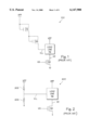
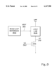
- FIG. 1 shows a nonvolatile memory circuit 100 that includes a nonvolatile memory cell 118 coupled to a load line circuit 112.
- the nonvolatile memory cell can be programmed by applying a gate voltage VG of approximately 12 volts, a drain voltage VD of approximately 7 -9 volts, and connecting the source terminal to ground. It is important to achieve and maintain these voltage ranges during programming of nonvolatile memory cell 118.
- a programming voltage VD is applied to the drain of nonvolatile memory cell 118 by load line circuit 112 in response to programming power supply voltage VPP and a load line control voltage VLL.
- VPP is typically 11 to 13 volts
- VLL is two threshold voltage drops less than VPP due to diode connected N-channel transistors 114 and 116.
- load line circuit 112 includes a transistor that has its gate coupled to VLL and another terminal coupled to VD such that VD is approximately one threshold drop below VLL.
- nonvolatile memory circuit 100 When nonvolatile memory circuit 100 is subjected to changes in process parameters (transistor channel lengths, widths, etc.), changes in operating temperatures, or changes in the programming supply voltage VPP, the load line voltage VLL, and consequently the programming voltage VD, vary. If VD varies too much, nonvolatile memory cell 118 may not be programmed correctly. For example, when process parameters are skewed to a fast process for n-channel transistors 114 and 116, the threshold voltages of these diode connected transistors will drop causing VLL and VD to increase accordingly. Similarly, as the operating temperature of nonvolatile memory circuit 100 increases, the threshold voltages of transistors 114 and 116 will increase causing VLL and VD to drop accordingly. Additionally, if VPP increases during operation of nonvolatile memory circuit 100, VLL and VD will increase accordingly.
- FIG. 2 shows another nonvolatile memory circuit 200 that generates a load line voltage VLL from a voltage divider or resistor divider configuration including resistors 202 and 204.
- VLL is generally less sensitive to process and temperature fluctuations as these variations will generally have the same impact on each of resistor 202 and 204.
- VLL does, however, vary will changes in the power supply programming voltage VPP such that programming voltage VD will vary with changes in VPP.
- a nonvolatile memory circuit that produces a load line voltage that does not substantially vary with changes in process parameters, operating temperatures, or changes in the power supply voltage applied to the circuit.
- a stable load line voltage may advantageously produce a programming voltage VD that may be maintained within a programming window in spite of changes in the operating conditions and process variations of the nonvolatile memory circuit.
- One embodiment of the present invention concerns a nonvolatile memory circuit that includes a load circuit coupled to a band-gap reference circuit and a nonvolatile memory cell.
- the load line circuit is configured to provide a programming voltage to the nonvolatile memory cell.
- the programming voltage may be generated in response to the reference voltage generated by the band-gap reference circuit.
- the nonvolatile memory circuit may also include an amplifying circuit that amplifies the reference voltage of the band-gap circuit, and provides the amplified reference voltage to the load circuit.
- the nonvolatile memory circuit may further include a voltage trim circuit that trims the amplified reference voltage and provides the trimmed amplified reference voltage to the load circuit.
- the reference voltage, amplified reference voltage, and the trimmed amplified reference voltage may each output a stable voltage that is independent of variations in process parameters, operating temperatures, and supply voltages of the nonvolatile memory circuit.
- FIG. 1 is conventional nonvolatile memory circuit
- FIG. 2 is another conventional nonvolatile memory circuit
- FIG. 3 is a block diagram of one embodiment of a nonvolatile memory circuit according to the present invention.
- FIG. 4 is a block diagram of another embodiment of a nonvolatile memory circuit according to the present invention.
- FIG. 5 is a circuit diagram of one embodiment of the nonvolatile memory circuit of FIG. 3;
- FIG. 6 is one embodiment of a voltage trim circuit
- FIG. 7 is another embodiment of a voltage trim circuit
- FIG. 8 is block diagram of another embodiment of a nonvolatile memory circuit according to the present invention.
- FIG. 9 is circuit diagram of one embodiment of a band-gap reference circuit.
- FIG. 10 is a block diagram of another embodiment of a nonvolatile memory circuit according to the present invention.
- a stable, adjustable programming voltage scheme for a nonvolatile memory device is disclosed.
- specific nomenclature is set forth to provide a thorough understanding of the present invention. However, it will be apparent to one skilled in the art that these specific details are not required to practice the present invention. In other instances, well known circuits and devices are shown in block diagram form to avoid obscuring the present invention unnecessarily.
- one embodiment of the present invention is a nonvolatile memory circuit that includes a load circuit coupled to a band-gap reference circuit and a nonvolatile memory cell.
- the load line circuit may be configured to provide a programming voltage to the nonvolatile memory cell in response to a reference voltage generated by the band-gap reference circuit.
- the nonvolatile memory circuit may also include an amplifying circuit that amplifies the reference voltage of the band-gap circuit, and provides the amplified reference voltage to the load circuit.
- the nonvolatile memory circuit may further include a voltage trim circuit that trims the amplified reference voltage and provides the trimmed amplified reference voltage to the load circuit.
- the reference voltage, amplified reference voltage, and the trimmed amplified reference voltage may each have a stable voltage that does not substantially vary with changes in process parameters (transistor channel lengths, widths, etc.), operating temperatures, and supply voltages of the nonvolatile memory circuit.
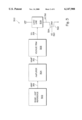
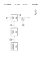
- FIG. 3 shows nonvolatile memory circuit 300 that is one embodiment of the present invention.
- Nonvolatile memory circuit 300 may include a nonvolatile memory cell 318 coupled to a load line circuit 308.
- Nonvolatile memory cell 318 may be a EPROM cell, EEPROM cell, or a flash cell that stores one or more states.
- Nonvolatile memory cell 318 includes a drain terminal coupled to load line circuit 308, a select gate 324 coupled to a gate voltage VG 320, a floating gate 322, and a source terminal that may be coupled to a ground voltage or approximately zero volts.
- Floating gate 322 may be an electrically isolated floating gate that traps charge.
- nonvolatile memory cell 318 may be programmed by applying approximately 10 volts to approximately 13 volts on VG 320 and a programming voltage VD 316 of approximately 7 volts to approximately 9 volts.
- the programming voltage VD 316 may be supplied in response to the programming supply voltage VPP and the load line control voltage VLL 314.
- the programming supply voltage VPP may be from approximately 10 volts to approximately 13 volts
- the load line control voltage VLL 314 may be from approximately 7 volts to approximately 10 volts.
- other voltages may be used.
- Load line circuit 308 may be any load line circuit that supplies the requisite programming voltage VD 316 and sufficient current to allow nonvolatile memory cell 318 to be programmed to a desired state.
- load line circuit 308 may be a resistor, a diode, and/or a transistor.
- load line circuit 308 includes a transistor that has its gate coupled to VLL 314, its drain coupled to VPP, and its source coupled to the drain of nonvolatile memory cell 318.
- the programming voltage VD 316 may be approximately one threshold drop below VLL 314.
- VLL 314 As the programming voltage VD 316 is dependent upon the load line control voltage VLL 314, is it desirable for VLL 314 to be a stable voltage that does not substantially vary with changes in operating conditions of nonvolatile memory circuit 300 including changes in process parameters (transistor channel lengths, widths, etc.) of the active and passive circuit elements, operating temperatures, and supply voltages of the nonvolatile memory circuit. When VLL 314 is stable, VD 316 may also be stable or independent of changes in the operation conditions of nonvolatile memory circuit 300.
- a stable load line control voltage VLL 314 and, consequently, a stable VD 316 may be generated from band-gap reference circuit 302, non-inverting operation amplifier 304, and from voltage trim circuit 306.
- Band-gap reference circuit 302 may be any band-gap reference circuit that generates a reference voltage VREF 310 that is substantially stable across expected, specified, simulated, or characterized operating conditions (e.g., process, supply voltage, and temperature) of nonvolatile memory circuit 300.
- Band-gap circuit 302 may generate VREF 310 having a voltage that is approximately the band-gap voltage of the material used to fabricate the circuit elements constituting band-gap reference circuit 302.
- VREF may be near the band-gap voltage of silicon of 1.12 volts.
- VREF for a silicon-based band-gap reference circuit may be approximately 1.25 volts.
- the circuit components are manufactured from a different material (e.g., germanium or gallium-arsenide), then VREF may be near the band-gap voltage of that material (e.g., 0.67 volts for germanium).
- Band-gap circuit 302 may also be designed to generate VREF 310 having a voltage that is a multiple of, or simply greater than, the band-gap voltage of the material used to manufacture the circuit components of band-gap reference circuit 302.
- amplifier circuit 304 may amplify VREF 310 to an amplified reference voltage VAMP 312 that is within the desired voltage range for VLL 314. While any amplifying circuit may be used to amplify VREF 310 to VAMP 312, amplifying circuit 304 preferably is a non-inverting operational amplifier that generates VAMP 312 as a stable voltage that does not substantially vary with changes in operating conditions of nonvolatile memory circuit 300.
- VAMP 312 may be directly connected to load line 308 as shown in FIG. 4, or may be coupled to voltage trim circuit 306 is in FIG. 3.
- Voltage trim circuit 306 provides a means for adjusting VAMP 312 to a desired voltage VLL 314 within a desired programming window.
- Voltage trim circuit 306 may be any means that generally outputs VLL 314 having a voltage that is less than or equal to VAMP 312.
- voltage trim circuit 306 may include a resistor, a voltage divider or resistor divider network, and/or transistors.
- the load line control voltage VLL 314 output by voltage trim circuit 306 may be programmable, and may be controlled by a control circuit (not shown), a register element (not shown), or may be externally controlled by a user or other circuitry.
- voltage trim circuit 306 includes circuit elements that will output VLL 314 as a stable voltage that does not substantially vary with changes in operating conditions of nonvolatile memory circuit 300.
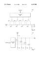
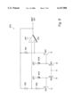
- FIG. 5 shows nonvolatile memory circuit 500 that is one embodiment of nonvolatile memory circuit 300 of FIG. 3.
- Nonvolatile memory circuit 500 includes band-gap reference circuit 502 that is one embodiment of band-gap reference circuit 302; non-inverting operational amplifier circuit 504 that is one embodiment of amplifier circuit 304; voltage trim circuit 506 that is one embodiment of voltage trim circuit 306; and, load line circuit 508 that is one embodiment of load line circuit 308 of FIG. 3.
- Each embodiment of circuits 502, 504, 506, and 508 of FIG. 5 may work with other embodiments of circuits 302, 304, 306, and/or 308 of FIG. 3.
- Band-gap reference circuit 502 includes operational amplifier 510 having its inverted input coupled a first terminal of each of resistors 512 and 516.
- the second terminal of resistor 512 is coupled to the output of operational amplifier 510.
- the second terminal of resistor 516 is coupled to the emitter of pnp bipolar transistor 518.
- Transistor 518 is configured as a diode having its base and collector coupled to ground or approximately zero volts.
- Operational amplifier 510 has its non-inverted input coupled to a first terminal of resistor 514 and the emitter of pnp bipolar transistor 520.
- the second terminal of resistor 514 is coupled to resistor 512 and the output of operational amplifier 510.
- Transistor 520 is also configured as a diode with its base and collector coupled to ground or approximately zero volts.
- diode-configured npn bipolar transistors may replace pnp bipolar transistors 518 and 520.
- Operational amplifier 510 may receive power from VCC that is generally supplied to an integrated circuit or system that includes nonvolatile memory circuit 500. Alternatively, operational amplifier 510 may receive programming power supply VPP.
- band-gap reference circuit 502 generates a reference voltage VREF 310 that is stable or has a variation of substantially zero as operating conditions (e.g., process parameters, operating temperatures, and supply voltage VCC) change for band-gap reference circuit 502 and nonvolatile memory circuit 500.
- VREF 310 may be determined according to equation one (1) below. ##EQU1##
- VBE 520 is the base-to-emitter voltage of transistor 520 (e.g., approximately 0.5 volts to approximately 0.8 volts)
- R 512 is the resistance of resistor 512
- R 514 is the resistance of resistors 514
- R 516 is the resistance of resistor 516
- I S518 is the saturation current of pnp transistor 518
- I S520 is the saturation current of pnp transistor 520
- k is Boltzman's constant and is equal to 8.62 ⁇ 10 -5 V/° K
- T is the operating temperature in ° K
- q is the magnitude of electronic charge and equal to 1.6 ⁇ 10 -19 coulombs.
- Equation one shows that VREF 310 comprises two terms: the first having a negative temperature coefficient (VBE 520 ); and, the second term having a positive temperature coefficient (kT/q). It is desirable to choose values of resistors 512, 514, 516, and saturation currents I S518 and I S520 that will yield a reference voltage VREF 310 that is stable across operation conditions. For silicon-based circuits, this results in VREF 310 being approximately 1.25 volts.
- Band-gap reference circuit 502 may be designed to output a different voltage; however, if VREF 310 is higher than approximately 1.25 volts the VREF may have a positive temperature coefficient, and if VREF 310 is lower than approximately 1.25 volts the VREF may have a negative temperature coefficient.
- resistors 512, 514, and 516 may be approximately 20 to 30 k ⁇ and resistor 516 may have approximately one tenth the resistance of resistors 512 and 514 (i.e., 2 to 3 k ⁇ ) when transistor 518 is sized to have a current density one eighth of that of transistor 520.
- Band-gap reference circuits such as band-gap reference circuit 502 have not previously been incorporated into a nonvolatile memory circuit to provide a stable reference voltage that may be used to generate a programming voltage for a nonvolatile memory cell.
- the prior art techniques of generating a load line control voltage using diode configured transistors or voltage divider schemes as in FIGS. 1 and 2 are easier to design and require considerably less silicon (or die) area to implement in an integrated circuit.
- nonvolatile memory circuit processes have generally been NMOS or CMOS processes that only have parasitic bipolar transistors. Steps are normally taken to reduce the influence of the parasitic bipolar transistors on the operation of the NMOS, PMOS, or CMOS transistors in the circuit.
- band-gap reference circuit 502 may advantageously make use of bipolar transistors 518 and 520 that may be present, for example, in a CMOS process.
- a BICMOS process may be used to provide both CMOS and bipolar transistors.
- Amplifier 504 is a non-inverting operational amplifier that may have its non-inverted input coupled to VREF 310, and its inverted input coupled to a first terminal of each of resistors 524 and 526. A second terminal of resistor 524 is coupled to the output of operational amplifier 522. A second terminal of resistor 526 is coupled to ground or approximately zero volts. Operational amplifier 510 may receive power from programming power supply VPP.
- Amplifier 504 may generate the amplified voltage VAMP 312, and may have a positive gain that may be controlled by the ratio of resistors 524 and 526 according to equation two (2). ##EQU2##
- R 524 is the resistance of resistor 524
- R 526 is the resistance of resistors 526.
- the resistance of resistors 524 and 526 may selected to provide any desired gain.
- amplifier circuit 504 generates VAMP 312 having a voltage of approximately eight (8) volts, VREF 310 is approximately 1.25 volts, resistor 524 is approximately 20 k ⁇ , and resistor 526 is approximately 3.7 k ⁇ .
- amplifier 504 produces VAMP 312 that is substantially independent VPP. Additionally, amplifier 504 produces VAMP 312 that is substantially independent of changes in process parameters and temperature changes. Temperature or process variations that affect the values of resistors 524 and 526 may have a similar impact on each resistor such that the gain of amplifier 504 will not substantially change with changes in operating conditions of amplifier 504 and/or nonvolatile memory circuit 500. Thus, amplifier 504 may generate an amplified reference signal provided by band-gap reference circuit 502, wherein the amplified reference voltage is generally independent of changes in operating conditions.
- VAMP 312 may be coupled to an input of voltage trim circuit 506.
- Voltage trim circuit 506 is one embodiment of a means for adjusting or trimming the amplified voltage VAMP 312 to a desired load line control voltage VLL 314 that may less than or equal to VAMP 312.
- Voltage trim circuit 506 may include resistors 530, 531, 532, and 533 coupled in series between VAMP 312 and ground.
- Voltage trim circuit 506 may also include pass transistors 534, 535, 536, and 537 each having a source (drain) terminal coupled to one or more of resistors 530-533, a drain (source) terminal coupled together and outputting VLL 314, and a gate coupled to decoder circuit 528.
- the source (drain) terminal of pass transistor 534 may be coupled to VAMP 312
- the source (drain) terminal of pass transistor 535 may be coupled at the interconnection of resistors 530 and 531
- the source (drain) terminal of pass transistor 536 may be coupled at the interconnection of resistors 531 and 532
- the source (drain) terminal of pass transistor 537 may be coupled at the interconnection of resistors 532 and 533.
- Pass transistors 534-537 may be NMOS or PMOS gates, CMOS transmission gates, or any other switch circuits.
- Resistors 530-533 form a voltage divider or a resistor divider network, and may be any values that may generate a desired load line control voltage VLL 314 from VAMP 312. For one embodiment, resistors 530-533 may be approximately 10 to 20 k ⁇ .
- Pass transistors 534-537 control which point in the voltage divider network may be tapped for VLL 314.
- One or more of pass transistors 534-537 may be turned on or off by decoder 528 in response to an address input.
- the address input may be supplied by control logic (not shown), from a register element (not shown), or from an external user or other circuitry.
- the gates of pass transistors 534-537 may be hard-wired to output a predetermined voltage to VLL 314 from the voltage divider network.
- pass transistors 534-537 may be replaced with programmable elements including fuses, flash memory cells, or other programmable elements.
- Voltage trim circuit 506 outputs VLL 314 that is generally independent of operating conditions because VLL 314 is dependent upon a voltage divider ratio that has a stable voltage VAMP 312 as its source. Temperature or process variations that affect the values of resistors 530-533 may have a similar impact on each resistor such that the voltage divider output of VLL 314 will not substantially change with changes in operating conditions. Additionally, decoder circuit 528 may provide pumped voltages to each gate terminal of pass transistors 534-537. The pumped voltages may be at least one threshold voltage greater than VLL 314 to reduce threshold voltage dependency of VLL 314.
- FIG. 6 shows voltage trim circuit 600 that is another embodiment of voltage trim circuit 306 of FIG. 3 and/or voltage trim circuit 506 of FIG. 5.
- Voltage trim circuit 600 includes resistors 602, 603, 604, and 605 coupled in series between VAMP 312 and VLL 314. Resistors 602-606 may be coupled in a voltage divider configuration with resistor 606 that is coupled between VLL 314 and ground.
- Voltage trim circuit 600 may also include transistors 607, 608, 609, and 610 each having a gate coupled to decoder circuit 612, and a source and drain terminal coupled to each terminal of resistors 602, 603, 604, and 605, respectively.
- Transistors 607-610 may be NMOS or PMOS gates, CMOS transmission gates, or any other switch circuits.
- Resistors 602-606 form a voltage divider or a resistor divider network, and may be any values that may generate a desired load line control voltage VLL 314 from VAMP 312.
- resistors 602-606 may be approximately 10 to 20 k ⁇ .
- Transistors 607-610 control which of resistors 602-605 may participate in generating VAMP 312.
- One or more of transistors 607-610 may be turned on or off by decoder 612 in response to an address input.
- the address input may be supplied by control logic (not shown), from a register element (not shown), or from an external user or other circuitry.
- the gates of transistors 607-610 may be hard-wired to output a predetermined voltage to VLL 314 from the voltage divider network.
- transistors 607-610 may be replaced with programmable elements including fuses, flash memory cells, or other programmable elements.
- Voltage trim circuit 600 outputs VLL 314 that is generally independent of operating conditions because VLL 314 is dependent upon a voltage divider ratio that has a stable voltage VAMP 312 as its source. Temperature or process variations that affect the values of resistors 602-606 may have a similar impact on each resistor such that the voltage divider output of VLL 314 will not substantially change with changes in operating conditions. Additionally, decoder circuit 612 may provide pumped voltages to each gate terminal of transistors 607-610. The pumped voltages may be at least one threshold voltage greater than VLL 314 to reduce any threshold voltage dependency of VLL 314.
- FIG. 7 shows voltage trim circuit 700 that is another embodiment of voltage trim circuit 306 of FIG. 3 and/or voltage trim circuit 506 of FIG. 5.
- Voltage trim circuit 700 includes resistors 703, 704, 705, and 706 coupled in parallel with each other and coupled in a voltage divider configuration with resistor 702.
- Resistor 702 may be coupled between VAMP 312 and VLL 314.
- Resistors 703, 704, 705, and 706 may be coupled to resistor 702 via pass transistors 707, 708, 709, and 710, respectively.
- Transistors 707, 708, 709, and 710 may alternatively be coupled between resistors 703, 704, 705, and 706, respectively, and ground.
- Transistors 707-710 may each have a gate coupled to decoder circuit 712.
- Transistors 707-710 may be NMOS or PMOS gates, CMOS transmission gates, or any other switch circuits.
- Resistors 702-706 form a voltage divider or a resistor divider network, and may be any values that may generate a desired load line control voltage VLL 314 from VAMP 312.
- resistors 702-706 may be approximately 10 to 20 k ⁇ .
- Transistors 707-710 control which of resistors 702-706 may participate in generating VLL 314.
- One or more of transistors 707-710 may be turned on or off by decoder 712 in response to an address input. The address input may be supplied by control logic (not shown), from a register element (not shown), or from an external user or other circuitry.
- the gates of transistors 707-710 may be hard-wired to output a predetermined voltage to VLL 314 from the voltage divider network.
- transistors 707-710 may be replaced with programmable elements including fuses, flash memory cells, or other programmable elements.
- Voltage trim circuit 700 outputs VLL 314 that is generally independent of operating conditions because VLL 314 is dependent upon a voltage divider ratio that has a stable voltage VAMP 312 as its source. Temperature or process variations that affect the values of resistors 702-706 may have a similar impact on each resistor such that the voltage divider output of VLL 314 will not substantially change with changes in operating conditions. Additionally, decoder circuit 712 may provide pumped voltages to each gate terminal of transistors 707-710. The pumped voltages may be at least one threshold voltage greater than VLL 314 to reduce any threshold voltage dependency of VLL 314.
- nonvolatile memory circuit 500 also includes load line circuit 508.
- Load line circuit 508 may provide the programming voltage VD 316 (and the requisite programming current) to the drain of nonvolatile memory cell 318 during programming of the cell.
- Load line circuit 508 may include resistor 538 and transistors 540, 542, and 544 coupled in series with each other and coupled between programming supply voltage VPP and the drain of nonvolatile memory cell 318.
- Resistor 538 may have one terminal coupled to programming supply voltage VPP, and another terminal coupled to the drain (source) of diode configured transistor 540.
- Transistor 540 may have its drain (source) coupled to the drain (source) of transistor 542.
- Transistor 542 may have its gate coupled to a pumped voltage VPUMP, and its source (drain) coupled to the drain (source) of transistor 544.
- the pumped voltage VPUMP may be at least one threshold voltage of transistor 542 greater than the voltage provided by transistor 540.
- Transistor 542 is optional and may be omitted.
- Transistor 544 has its source (drain) coupled to the drain of nonvolatile memory cell 318, and its gate configured to receive VLL 314.
- the programming voltage VD 316 may be approximately equal to a VLL 314 minus a threshold voltage drop across transistor 544.
- the more stable or independent that the load line control voltage VLL 314 is with respect to variations in operating conditions of nonvolatile memory circuit 500 the more stable or independent the programming voltage VD 316 is with respect to variations in operating conditions of nonvolatile memory circuit 500.
- load line circuit 508 may also be used for nonvolatile memory circuit 500, including just transistor 544, a voltage divider network, and/or any combination of a transistor and resistor circuit.
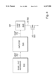
- nonvolatile memory circuit 300 may omit voltage trim circuit 304 as illustrated in FIG. 4.
- both amplifier circuit 304 and voltage trim circuit 306 may be omitted as shown in FIG. 8.
- band-gap reference circuit 302 may output reference voltage VREF 310 that may be sufficient to enable load line 308 to provide an adequate programming voltage VD 316 to nonvolatile memory circuit 318.
- band-gap reference circuit 302 may generate a reference voltage VREF 310 of approximately 7 volts to approximately 10 volts.
- FIG. 9 band-gap reference circuit 902 that is one embodiment of band-gap reference circuit 302 of FIG. 8 and/or FIG. 3.
- Band-gap reference circuit 902 has a similar configuration to band-gap reference circuit 502 of FIG. 5, except that band-gap reference circuit 902 is able to generate multiples of VREF 310 output by band-gap reference circuit 502. For each multiple increase in VREF 310, band-gap reference circuit 902 adds a bias current and pnp bipolar transistor pair to each of the non-inverted and inverted inputs of operational amplifier 510.
- current source 904 and pnp transistor 906 may be coupled to the base of pnp transistor 518.
- current source 908 and pnp transistor 910 may be coupled to the base of pnp transistor 520 as shown in FIG. 9.
- Band-gap reference circuit 902 may add additional pairs of current sources and transistors to each input of operational amplifier 510 to boost VREF 310 to any desired multiple of VREF 310 of FIG. 5 (i.e., a desired multiple of approximately 1.25 volts). For one embodiment, seven pairs of current sources and transistors may be added to each input of operational amplifier 510 to boost VREF 310 to approximately 8.75 volts.
- band-gap reference circuits generally known in the art may be used to provide any desired reference voltage directly to load line circuit 308.
- FIG. 8 may also include voltage trim circuit 306 coupled between band-gap reference circuit 302 and load line circuit 308 as shown in FIG. 10.
- Voltage trim circuit 306 may provide a means for adjusting VREF 310 output by band-gap reference circuit 302 to any desired voltage VLL 314 for load line circuit 308.
- FIGS. 5, 6, and 7 show exemplary embodiments of voltage trim circuit 306.
Abstract
Description
Claims (19)
Priority Applications (1)
| Application Number | Priority Date | Filing Date | Title |
|---|---|---|---|
| US08/962,860 US6147908A (en) | 1997-11-03 | 1997-11-03 | Stable adjustable programming voltage scheme |
Applications Claiming Priority (1)
| Application Number | Priority Date | Filing Date | Title |
|---|---|---|---|
| US08/962,860 US6147908A (en) | 1997-11-03 | 1997-11-03 | Stable adjustable programming voltage scheme |
Publications (1)
| Publication Number | Publication Date |
|---|---|
| US6147908A true US6147908A (en) | 2000-11-14 |
Family
ID=25506429
Family Applications (1)
| Application Number | Title | Priority Date | Filing Date |
|---|---|---|---|
| US08/962,860 Expired - Lifetime US6147908A (en) | 1997-11-03 | 1997-11-03 | Stable adjustable programming voltage scheme |
Country Status (1)
| Country | Link |
|---|---|
| US (1) | US6147908A (en) |
Cited By (21)
| Publication number | Priority date | Publication date | Assignee | Title |
|---|---|---|---|---|
| US20020016932A1 (en) * | 2000-06-23 | 2002-02-07 | Kabushiki Kaisha Toshiba | Semiconductor integrated circuit and semiconductor apparatus system |
| US6353560B1 (en) * | 1999-11-30 | 2002-03-05 | Sharp Kabushiki Kaisha | Semiconductor memory device |
| US6457093B2 (en) * | 1998-06-30 | 2002-09-24 | Micron Technology, Inc. | Circuit and method to control operations of another circuit |
| US6738298B1 (en) | 2002-11-18 | 2004-05-18 | Micron Technology, Inc. | Automatic reference voltage regulation in a memory device |
| US6774612B1 (en) * | 2002-10-18 | 2004-08-10 | Cisco Technology, Inc. | Device and method for reducing DC/DC converter initial set-point error and margining error |
| US7019585B1 (en) | 2003-03-25 | 2006-03-28 | Cypress Semiconductor Corporation | Method and circuit for adjusting a reference voltage signal |
| US20060152991A1 (en) * | 2004-10-26 | 2006-07-13 | Hyun-Duk Cho | Non-volatile memory storage of fuse information |
| US20060176043A1 (en) * | 2005-02-08 | 2006-08-10 | Denso Corporation | Reference voltage circuit |
| US20070159237A1 (en) * | 2006-01-12 | 2007-07-12 | Micron Technology, Inc. | Semiconductor temperature sensor using bandgap generator circuit |
| US7245536B1 (en) * | 2006-02-15 | 2007-07-17 | Catalyst Semiconductor, Inc. | Precision non-volatile CMOS reference circuit |
| US20070189355A1 (en) * | 2006-02-16 | 2007-08-16 | Harald Lorenz | Method and apparatus for calibration of an on-chip temperature sensor within a memory device |
| WO2007097933A2 (en) * | 2006-02-15 | 2007-08-30 | Catalyst Semiconductor, Inc. | Precision non-volatile cmos reference circuit |
| US20070203661A1 (en) * | 2006-02-28 | 2007-08-30 | Texas Instruments, Inc. | Trimming for accurate reference voltage |
| US20080116875A1 (en) * | 2006-11-16 | 2008-05-22 | Fan Yung Ma | Systems, apparatus and methods relating to bandgap circuits |
| US20080279254A1 (en) * | 2006-01-04 | 2008-11-13 | Micron Technology, Inc. | Semiconductor temperature sensor with high sensitivity |
| US20090161464A1 (en) * | 2007-12-21 | 2009-06-25 | Midorikawa Tatsuro | Semiconductor memory device |
| US20100177550A1 (en) * | 2009-01-14 | 2010-07-15 | Kabushiki Kaisha Toshiba | Nonvolatile semiconductor memory |
| CN103092244A (en) * | 2011-10-28 | 2013-05-08 | 爱思开海力士有限公司 | Multi-regulator circuit and integrated circuit including the same |
| US8618786B1 (en) * | 2009-08-31 | 2013-12-31 | Altera Corporation | Self-biased voltage regulation circuitry for memory |
| US9939827B1 (en) * | 2011-12-16 | 2018-04-10 | Altera Corporation | Temperature dependent power supply circuitry |
| US20220121259A1 (en) * | 2020-10-21 | 2022-04-21 | Dell Products, Lp | Systems and methods for flexible motherboard supporting flexible processor utilization for optimized design |
Citations (10)
| Publication number | Priority date | Publication date | Assignee | Title |
|---|---|---|---|---|
| US4723108A (en) * | 1986-07-16 | 1988-02-02 | Cypress Semiconductor Corporation | Reference circuit |
| US5061862A (en) * | 1989-07-11 | 1991-10-29 | Nec Corporation | Reference voltage generating circuit |
| US5402370A (en) * | 1993-09-10 | 1995-03-28 | Intel Corporation | Circuitry and method for selecting a drain programming voltage for a nonvolatile memory |
| US5444659A (en) * | 1990-09-11 | 1995-08-22 | Kabushiki Kaisha Toshiba | Semiconductor memory device having means for monitoring bias voltage |
| US5444656A (en) * | 1994-06-02 | 1995-08-22 | Intel Corporation | Apparatus for fast internal reference cell trimming |
| US5497119A (en) * | 1994-06-01 | 1996-03-05 | Intel Corporation | High precision voltage regulation circuit for programming multilevel flash memory |
| US5568425A (en) * | 1996-02-02 | 1996-10-22 | Integrated Silicon Solution, Inc. | Program drain voltage control for EPROM/flash |
| US5576990A (en) * | 1993-12-31 | 1996-11-19 | Sgs-Thomson Microelectronics, S.R.L. | Voltage regulator for non-volatile semiconductor memory devices |
| US5629611A (en) * | 1994-08-26 | 1997-05-13 | Sgs-Thomson Microelectronics Limited | Current generator circuit for generating substantially constant current |
| US5712815A (en) * | 1996-04-22 | 1998-01-27 | Advanced Micro Devices, Inc. | Multiple bits per-cell flash EEPROM capable of concurrently programming and verifying memory cells and reference cells |
-
1997
- 1997-11-03 US US08/962,860 patent/US6147908A/en not_active Expired - Lifetime
Patent Citations (11)
| Publication number | Priority date | Publication date | Assignee | Title |
|---|---|---|---|---|
| US4723108A (en) * | 1986-07-16 | 1988-02-02 | Cypress Semiconductor Corporation | Reference circuit |
| US5061862A (en) * | 1989-07-11 | 1991-10-29 | Nec Corporation | Reference voltage generating circuit |
| US5444659A (en) * | 1990-09-11 | 1995-08-22 | Kabushiki Kaisha Toshiba | Semiconductor memory device having means for monitoring bias voltage |
| US5402370A (en) * | 1993-09-10 | 1995-03-28 | Intel Corporation | Circuitry and method for selecting a drain programming voltage for a nonvolatile memory |
| US5576990A (en) * | 1993-12-31 | 1996-11-19 | Sgs-Thomson Microelectronics, S.R.L. | Voltage regulator for non-volatile semiconductor memory devices |
| US5497119A (en) * | 1994-06-01 | 1996-03-05 | Intel Corporation | High precision voltage regulation circuit for programming multilevel flash memory |
| US5546042A (en) * | 1994-06-01 | 1996-08-13 | Intel Corporation | High precision voltage regulation circuit for programming multiple bit flash memory |
| US5444656A (en) * | 1994-06-02 | 1995-08-22 | Intel Corporation | Apparatus for fast internal reference cell trimming |
| US5629611A (en) * | 1994-08-26 | 1997-05-13 | Sgs-Thomson Microelectronics Limited | Current generator circuit for generating substantially constant current |
| US5568425A (en) * | 1996-02-02 | 1996-10-22 | Integrated Silicon Solution, Inc. | Program drain voltage control for EPROM/flash |
| US5712815A (en) * | 1996-04-22 | 1998-01-27 | Advanced Micro Devices, Inc. | Multiple bits per-cell flash EEPROM capable of concurrently programming and verifying memory cells and reference cells |
Non-Patent Citations (2)
| Title |
|---|
| Paul R. Gray, et al., University of California, Berkeley, "Analysis and Design of Analog Integrated Circuits, Second Edition", 1984, pp. 295-296 & 515-517. |
| Paul R. Gray, et al., University of California, Berkeley, Analysis and Design of Analog Integrated Circuits, Second Edition , 1984, pp. 295 296 & 515 517. * |
Cited By (42)
| Publication number | Priority date | Publication date | Assignee | Title |
|---|---|---|---|---|
| US6457093B2 (en) * | 1998-06-30 | 2002-09-24 | Micron Technology, Inc. | Circuit and method to control operations of another circuit |
| US6353560B1 (en) * | 1999-11-30 | 2002-03-05 | Sharp Kabushiki Kaisha | Semiconductor memory device |
| US20020016932A1 (en) * | 2000-06-23 | 2002-02-07 | Kabushiki Kaisha Toshiba | Semiconductor integrated circuit and semiconductor apparatus system |
| US6774612B1 (en) * | 2002-10-18 | 2004-08-10 | Cisco Technology, Inc. | Device and method for reducing DC/DC converter initial set-point error and margining error |
| US20040190348A1 (en) * | 2002-11-18 | 2004-09-30 | Micron Technology, Inc. | Automatic reference voltage regulation in a memory device |
| US20040095810A1 (en) * | 2002-11-18 | 2004-05-20 | Micron Technology, Inc. | Automatic reference voltage regulation in a memory device |
| US6738298B1 (en) | 2002-11-18 | 2004-05-18 | Micron Technology, Inc. | Automatic reference voltage regulation in a memory device |
| US6842385B2 (en) | 2002-11-18 | 2005-01-11 | Micron Technology, Inc. | Automatic reference voltage regulation in a memory device |
| US7019585B1 (en) | 2003-03-25 | 2006-03-28 | Cypress Semiconductor Corporation | Method and circuit for adjusting a reference voltage signal |
| US20060152991A1 (en) * | 2004-10-26 | 2006-07-13 | Hyun-Duk Cho | Non-volatile memory storage of fuse information |
| US20060176043A1 (en) * | 2005-02-08 | 2006-08-10 | Denso Corporation | Reference voltage circuit |
| US7233136B2 (en) * | 2005-02-08 | 2007-06-19 | Denso Corporation | Circuit for outputting stable reference voltage against variation of background temperature or variation of voltage of power source |
| US8540423B2 (en) | 2006-01-04 | 2013-09-24 | Micron Technology, Inc. | Semiconductor temperature sensor with high sensitivity |
| US9464942B2 (en) | 2006-01-04 | 2016-10-11 | Micron Technology, Inc. | Semiconductor temperature sensor with high sensitivity |
| US20080279254A1 (en) * | 2006-01-04 | 2008-11-13 | Micron Technology, Inc. | Semiconductor temperature sensor with high sensitivity |
| US20070159237A1 (en) * | 2006-01-12 | 2007-07-12 | Micron Technology, Inc. | Semiconductor temperature sensor using bandgap generator circuit |
| US20100283530A1 (en) * | 2006-01-12 | 2010-11-11 | Micron Technology, Inc. | Semiconductor Temperature Sensor Using Bandgap Generator Circuit |
| US7821321B2 (en) * | 2006-01-12 | 2010-10-26 | Micron Technology, Inc. | Semiconductor temperature sensor using bandgap generator circuit |
| US8405447B2 (en) | 2006-01-12 | 2013-03-26 | Micron Technology, Inc. | Semiconductor temperature sensor using bandgap generator circuit |
| US7978000B2 (en) * | 2006-01-12 | 2011-07-12 | Micron Technology, Inc. | Semiconductor temperature sensor using bandgap generator circuit |
| WO2007097933A2 (en) * | 2006-02-15 | 2007-08-30 | Catalyst Semiconductor, Inc. | Precision non-volatile cmos reference circuit |
| US7324380B2 (en) | 2006-02-15 | 2008-01-29 | Catalyst Semiconductor, Inc. | Method for trimming the temperature coefficient of a floating gate voltage reference |
| US20070189069A1 (en) * | 2006-02-15 | 2007-08-16 | Catalyst Semiconductor, Inc. | Precision Non-Volatile CMOS Reference Circuit |
| WO2007097933A3 (en) * | 2006-02-15 | 2008-07-31 | Catalyst Semiconductor Inc | Precision non-volatile cmos reference circuit |
| US7245536B1 (en) * | 2006-02-15 | 2007-07-17 | Catalyst Semiconductor, Inc. | Precision non-volatile CMOS reference circuit |
| US20070189355A1 (en) * | 2006-02-16 | 2007-08-16 | Harald Lorenz | Method and apparatus for calibration of an on-chip temperature sensor within a memory device |
| US7383144B2 (en) * | 2006-02-16 | 2008-06-03 | Infineon Technologies Ag | Method and apparatus for calibration of an on-chip temperature sensor within a memory device |
| US7272523B1 (en) * | 2006-02-28 | 2007-09-18 | Texas Instruments Incorporated | Trimming for accurate reference voltage |
| US20070203661A1 (en) * | 2006-02-28 | 2007-08-30 | Texas Instruments, Inc. | Trimming for accurate reference voltage |
| US20080116875A1 (en) * | 2006-11-16 | 2008-05-22 | Fan Yung Ma | Systems, apparatus and methods relating to bandgap circuits |
| US7633333B2 (en) * | 2006-11-16 | 2009-12-15 | Infineon Technologies Ag | Systems, apparatus and methods relating to bandgap circuits |
| US7864614B2 (en) * | 2007-12-21 | 2011-01-04 | Kabushiki Kaisha Toshiba | Semiconductor memory device |
| US20090161464A1 (en) * | 2007-12-21 | 2009-06-25 | Midorikawa Tatsuro | Semiconductor memory device |
| US7924598B2 (en) * | 2009-01-14 | 2011-04-12 | Kabushiki Kaisha Toshiba | Nonvolatile semiconductor memory |
| US20100177550A1 (en) * | 2009-01-14 | 2010-07-15 | Kabushiki Kaisha Toshiba | Nonvolatile semiconductor memory |
| US8618786B1 (en) * | 2009-08-31 | 2013-12-31 | Altera Corporation | Self-biased voltage regulation circuitry for memory |
| CN103092244A (en) * | 2011-10-28 | 2013-05-08 | 爱思开海力士有限公司 | Multi-regulator circuit and integrated circuit including the same |
| CN103092244B (en) * | 2011-10-28 | 2016-03-16 | 爱思开海力士有限公司 | Multi-regulator circuit and the integrated circuit comprising multi-regulator circuit |
| TWI576851B (en) * | 2011-10-28 | 2017-04-01 | 愛思開海力士有限公司 | Multi-regulator circuit and integrated circuit including the same |
| US9939827B1 (en) * | 2011-12-16 | 2018-04-10 | Altera Corporation | Temperature dependent power supply circuitry |
| US20220121259A1 (en) * | 2020-10-21 | 2022-04-21 | Dell Products, Lp | Systems and methods for flexible motherboard supporting flexible processor utilization for optimized design |
| US11507164B2 (en) * | 2020-10-21 | 2022-11-22 | Dell Products, Lp | Systems and methods for flexible motherboard supporting flexible processor utilization for optimized design |
Similar Documents
| Publication | Publication Date | Title |
|---|---|---|
| US6147908A (en) | Stable adjustable programming voltage scheme | |
| US5898335A (en) | High voltage generator circuit | |
| EP0576774B1 (en) | Voltage regulator for memory devices | |
| US6943617B2 (en) | Low voltage CMOS bandgap reference | |
| JP2823822B2 (en) | Current generator circuit for generating an almost constant reference current | |
| US5838188A (en) | Reference voltage generation circuit | |
| US6894473B1 (en) | Fast bandgap reference circuit for use in a low power supply A/D booster | |
| KR0122103B1 (en) | The fuse device of a semiconductor memory equipment | |
| JPH0528777A (en) | Nonvolatile semiconductor memory | |
| US4673866A (en) | Constant voltage generator using memory transistors | |
| JP3450629B2 (en) | Negative voltage detection circuit and nonvolatile semiconductor memory device | |
| US20050052223A1 (en) | Programmable analog bias circuits using floating gate cmos technology | |
| JP4443205B2 (en) | Current drive circuit | |
| JPH0529996B2 (en) | ||
| US20210325261A1 (en) | Temperature sensor and memory device having same | |
| EP0661715B1 (en) | Non-volatile electrically programmable semiconductor memory device comprising a voltage regulator | |
| US6184670B1 (en) | Memory cell voltage regulator with temperature correlated voltage generator circuit | |
| US6906957B2 (en) | Sensing circuitry for reading and verifying the contents of electrically programmable and erasable non-volatile memory cells, useful in low supply-voltage technologies | |
| US20030202380A1 (en) | Band-gap voltage reference | |
| US6882582B2 (en) | EEPROM circuit voltage reference circuit and method for providing a low temperature-coefficient voltage reference | |
| US7019581B1 (en) | Current sense circuit | |
| KR100364428B1 (en) | High voltage regulation circuit | |
| EP0864158A1 (en) | Power supply independent current source for flash eprom erasure | |
| US7268622B2 (en) | Analog preamplifier calibration | |
| JP3355478B2 (en) | Reference voltage generation circuit |
Legal Events
| Date | Code | Title | Description |
|---|---|---|---|
| AS | Assignment |
Owner name: CYPRESS SEMICONDUCTOR CORPORATION, CALIFORNIA Free format text: ASSIGNMENT OF ASSIGNORS INTEREST;ASSIGNORS:ABUGHARBIEH, KHALDOON;YU, DONALD Y.;BETTMAN, ROGER J.;REEL/FRAME:008809/0498 Effective date: 19971103 |
|
| STCF | Information on status: patent grant |
Free format text: PATENTED CASE |
|
| FEPP | Fee payment procedure |
Free format text: PAYOR NUMBER ASSIGNED (ORIGINAL EVENT CODE: ASPN); ENTITY STATUS OF PATENT OWNER: LARGE ENTITY |
|
| FPAY | Fee payment |
Year of fee payment: 4 |
|
| FEPP | Fee payment procedure |
Free format text: PAYER NUMBER DE-ASSIGNED (ORIGINAL EVENT CODE: RMPN); ENTITY STATUS OF PATENT OWNER: LARGE ENTITY Free format text: PAYOR NUMBER ASSIGNED (ORIGINAL EVENT CODE: ASPN); ENTITY STATUS OF PATENT OWNER: LARGE ENTITY |
|
| FPAY | Fee payment |
Year of fee payment: 8 |
|
| FPAY | Fee payment |
Year of fee payment: 12 |
|
| AS | Assignment |
Owner name: MORGAN STANLEY SENIOR FUNDING, INC., NEW YORK Free format text: SECURITY INTEREST;ASSIGNORS:CYPRESS SEMICONDUCTOR CORPORATION;SPANSION LLC;REEL/FRAME:035240/0429 Effective date: 20150312 |
|
| AS | Assignment |
Owner name: CYPRESS SEMICONDUCTOR CORPORATION, CALIFORNIA Free format text: PARTIAL RELEASE OF SECURITY INTEREST IN PATENTS;ASSIGNOR:MORGAN STANLEY SENIOR FUNDING, INC., AS COLLATERAL AGENT;REEL/FRAME:039708/0001 Effective date: 20160811 Owner name: SPANSION LLC, CALIFORNIA Free format text: PARTIAL RELEASE OF SECURITY INTEREST IN PATENTS;ASSIGNOR:MORGAN STANLEY SENIOR FUNDING, INC., AS COLLATERAL AGENT;REEL/FRAME:039708/0001 Effective date: 20160811 |
|
| AS | Assignment |
Owner name: MONTEREY RESEARCH, LLC, CALIFORNIA Free format text: ASSIGNMENT OF ASSIGNORS INTEREST;ASSIGNOR:CYPRESS SEMICONDUCTOR CORPORATION;REEL/FRAME:040911/0238 Effective date: 20160811 |
|
| AS | Assignment |
Owner name: MORGAN STANLEY SENIOR FUNDING, INC., NEW YORK Free format text: CORRECTIVE ASSIGNMENT TO CORRECT THE 8647899 PREVIOUSLY RECORDED ON REEL 035240 FRAME 0429. ASSIGNOR(S) HEREBY CONFIRMS THE SECURITY INTERST;ASSIGNORS:CYPRESS SEMICONDUCTOR CORPORATION;SPANSION LLC;REEL/FRAME:058002/0470 Effective date: 20150312 |