US6150261A - Method of fabricating semiconductor device for preventing antenna effect - Google Patents
Method of fabricating semiconductor device for preventing antenna effect Download PDFInfo
- Publication number
- US6150261A US6150261A US09/318,235 US31823599A US6150261A US 6150261 A US6150261 A US 6150261A US 31823599 A US31823599 A US 31823599A US 6150261 A US6150261 A US 6150261A
- Authority
- US
- United States
- Prior art keywords
- layer
- opening
- forming
- metallic
- tungsten
- Prior art date
- Legal status (The legal status is an assumption and is not a legal conclusion. Google has not performed a legal analysis and makes no representation as to the accuracy of the status listed.)
- Expired - Lifetime
Links
Images

Classifications
-
- H—ELECTRICITY
- H01—ELECTRIC ELEMENTS
- H01L—SEMICONDUCTOR DEVICES NOT COVERED BY CLASS H10
- H01L24/00—Arrangements for connecting or disconnecting semiconductor or solid-state bodies; Methods or apparatus related thereto
- H01L24/01—Means for bonding being attached to, or being formed on, the surface to be connected, e.g. chip-to-package, die-attach, "first-level" interconnects; Manufacturing methods related thereto
- H01L24/02—Bonding areas ; Manufacturing methods related thereto
-
- H—ELECTRICITY
- H01—ELECTRIC ELEMENTS
- H01L—SEMICONDUCTOR DEVICES NOT COVERED BY CLASS H10
- H01L21/00—Processes or apparatus adapted for the manufacture or treatment of semiconductor or solid state devices or of parts thereof
- H01L21/70—Manufacture or treatment of devices consisting of a plurality of solid state components formed in or on a common substrate or of parts thereof; Manufacture of integrated circuit devices or of parts thereof
- H01L21/71—Manufacture of specific parts of devices defined in group H01L21/70
- H01L21/768—Applying interconnections to be used for carrying current between separate components within a device comprising conductors and dielectrics
- H01L21/76838—Applying interconnections to be used for carrying current between separate components within a device comprising conductors and dielectrics characterised by the formation and the after-treatment of the conductors
- H01L21/76886—Modifying permanently or temporarily the pattern or the conductivity of conductive members, e.g. formation of alloys, reduction of contact resistances
- H01L21/76892—Modifying permanently or temporarily the pattern or the conductivity of conductive members, e.g. formation of alloys, reduction of contact resistances modifying the pattern
-
- H—ELECTRICITY
- H01—ELECTRIC ELEMENTS
- H01L—SEMICONDUCTOR DEVICES NOT COVERED BY CLASS H10
- H01L2924/00—Indexing scheme for arrangements or methods for connecting or disconnecting semiconductor or solid-state bodies as covered by H01L24/00
- H01L2924/01—Chemical elements
- H01L2924/01005—Boron [B]
-
- H—ELECTRICITY
- H01—ELECTRIC ELEMENTS
- H01L—SEMICONDUCTOR DEVICES NOT COVERED BY CLASS H10
- H01L2924/00—Indexing scheme for arrangements or methods for connecting or disconnecting semiconductor or solid-state bodies as covered by H01L24/00
- H01L2924/01—Chemical elements
- H01L2924/01006—Carbon [C]
-
- H—ELECTRICITY
- H01—ELECTRIC ELEMENTS
- H01L—SEMICONDUCTOR DEVICES NOT COVERED BY CLASS H10
- H01L2924/00—Indexing scheme for arrangements or methods for connecting or disconnecting semiconductor or solid-state bodies as covered by H01L24/00
- H01L2924/01—Chemical elements
- H01L2924/01014—Silicon [Si]
-
- H—ELECTRICITY
- H01—ELECTRIC ELEMENTS
- H01L—SEMICONDUCTOR DEVICES NOT COVERED BY CLASS H10
- H01L2924/00—Indexing scheme for arrangements or methods for connecting or disconnecting semiconductor or solid-state bodies as covered by H01L24/00
- H01L2924/01—Chemical elements
- H01L2924/01015—Phosphorus [P]
-
- H—ELECTRICITY
- H01—ELECTRIC ELEMENTS
- H01L—SEMICONDUCTOR DEVICES NOT COVERED BY CLASS H10
- H01L2924/00—Indexing scheme for arrangements or methods for connecting or disconnecting semiconductor or solid-state bodies as covered by H01L24/00
- H01L2924/01—Chemical elements
- H01L2924/01022—Titanium [Ti]
-
- H—ELECTRICITY
- H01—ELECTRIC ELEMENTS
- H01L—SEMICONDUCTOR DEVICES NOT COVERED BY CLASS H10
- H01L2924/00—Indexing scheme for arrangements or methods for connecting or disconnecting semiconductor or solid-state bodies as covered by H01L24/00
- H01L2924/01—Chemical elements
- H01L2924/01033—Arsenic [As]
-
- H—ELECTRICITY
- H01—ELECTRIC ELEMENTS
- H01L—SEMICONDUCTOR DEVICES NOT COVERED BY CLASS H10
- H01L2924/00—Indexing scheme for arrangements or methods for connecting or disconnecting semiconductor or solid-state bodies as covered by H01L24/00
- H01L2924/01—Chemical elements
- H01L2924/0105—Tin [Sn]
-
- H—ELECTRICITY
- H01—ELECTRIC ELEMENTS
- H01L—SEMICONDUCTOR DEVICES NOT COVERED BY CLASS H10
- H01L2924/00—Indexing scheme for arrangements or methods for connecting or disconnecting semiconductor or solid-state bodies as covered by H01L24/00
- H01L2924/01—Chemical elements
- H01L2924/01074—Tungsten [W]
-
- H—ELECTRICITY
- H01—ELECTRIC ELEMENTS
- H01L—SEMICONDUCTOR DEVICES NOT COVERED BY CLASS H10
- H01L2924/00—Indexing scheme for arrangements or methods for connecting or disconnecting semiconductor or solid-state bodies as covered by H01L24/00
- H01L2924/049—Nitrides composed of metals from groups of the periodic table
- H01L2924/0494—4th Group
- H01L2924/04941—TiN
-
- H—ELECTRICITY
- H01—ELECTRIC ELEMENTS
- H01L—SEMICONDUCTOR DEVICES NOT COVERED BY CLASS H10
- H01L2924/00—Indexing scheme for arrangements or methods for connecting or disconnecting semiconductor or solid-state bodies as covered by H01L24/00
- H01L2924/10—Details of semiconductor or other solid state devices to be connected
- H01L2924/11—Device type
- H01L2924/13—Discrete devices, e.g. 3 terminal devices
- H01L2924/1304—Transistor
- H01L2924/1306—Field-effect transistor [FET]
- H01L2924/13091—Metal-Oxide-Semiconductor Field-Effect Transistor [MOSFET]
Definitions
- the present invention relates to a semiconductor fabrication method. More particularly, the present invention relates to a method of fabricating a semiconductor device for preventing an antenna effect.
- the antenna effect is one of the most common factors related to the stability of a device occurred in a plasma process.
- the antenna effect arises from a plasma-etching process. During the plasma-etching process, electrons and positive ions (e - and p + ) decompose from the surface of a substrate by an ionization reaction. These charged particles move outward through conductive wires having lowest resistance. This causes the antenna effect.
- the strength of the antenna effect is proportional to an antenna ratio of area (A A ) or an antenna ratio of perimeter (A p ). The higher the antenna ratio is, the stronger the antenna effect is.
- Antenna ratio of area A A is defined as:
- M A is the area of an interconnect metallic layer and G A is the area of a gate.
- Antenna ratio of perimeter A P is defined as:
- M P is the perimeter of an interconnect metallic layer and G P is the perimeter of a gate.
- the antenna effect is reduced.
- the antenna ratio is decreased.
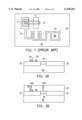
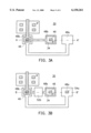
- FIG. 1 illustrates top view of a conventional device for preventing an antenna effect.
- a substrate 10 comprises a transistor T1, such as a metal oxide semiconductor (MOS) transistor.
- a transistor gate 12 is electrically connected to the metallic layer via a polysilicon interconnection 14 on the substrate 10.
- the metallic layer 16 is electrically coupled with a detector 20, which detects the antenna effect, through a contact 18.
- the conventional detector 20 further comprises a protection diode on the metallic layer 16.
- the protection diode is formed to prevent an antenna effect from occurring in the metallic layer 16 and damaging T1.
- the diode cannot effectively prevent the damage caused by charged carrier produced by positive/negative bias during the plasma process, and thus, the protection is limited.
- the invention provides a method of fabricating a semiconductor device for preventing an antenna effect.
- An isolation structure is formed in a semiconductor substrate to define an active region next to the isolation structure.
- a gate comprising a polysilicon layer is formed on the isolation structure.
- a dielectric layer is formed over the substrate. The dielectric layer is patterned to form a first opening and a second opening. The first opening exposes a portion of the substrate in the active region, and the second opening exposes a portion of the polysilicon layer of the gate.
- a conductive layer is formed on the dielectric layer to fill the first opening and the second opening. A portion of the conductive layer is removed until the surface of the conductive layer is level with the surface of the dielectric layer.
- a patterned metallic layer exposing a portion of the dielectric layer is formed.
- the metallic layer comprises a first metallic layer and a second metallic layer.
- the first metallic layer covers a portion of the dielectric layer
- the second metallic layer covers the conductive layer and a portion of the dielectric layer.
- a dielectric layer is formed over the substrate.
- the dielectric layer is patterned to form a first opening and a second opening.
- the first opening exposes a portion of the first metallic layer
- the second opening exposes a portion of the second metallic layer.
- a glue/barrier layer and a tungsten layer are formed over the substrate. Portions of the tungsten layer and the glue/barrier layer are removed to form a tungsten plug in the first opening and a tungsten spacer on a sidewall of the second opening.
- a third metallic layer is formed over the substrate.
- a patterned photoresist layer is formed on the third metallic layer above the tungsten plug. A portion of the third metallic layer and the second metallic layer are removed with the photoresist layer and the tungsten spacer serving as masks. The photoresist layer and the spacer are removed.
- the invention prevents the occurrence of an antenna effect.
- the reliability of the semiconductor device thus is increased.
- FIG. 1 is a schematic, top view of a conventional device for preventing an antenna effect
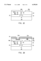
- FIGS. 2A through 2H are schematic, cross-sectional views showing a method of fabricating a semiconductor structure for preventing an antenna effect according to one preferred embodiment of the invention
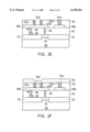
- FIG. 3A is a schematic, top view of the structure depicted in FIG. 2C, wherein FIG. 2C is a schematic, cross-sectional view of FIG. 3A taken along line A-A';
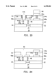
- FIG. 3B is a schematic, top view of the structure depicted in FIG. 2E, wherein FIG. 2E is a schematic, cross-sectional view of FIG. 3B taken along line B-B'; and
- FIG. 3C is a schematic, top view of the structure depicted in FIG. 2H, wherein FIG. 2H is a schematic, cross-sectional view of FIG. 3C taken along line C-C'.
- FIGS. 2A through 2H are schematic, cross-sectional views showing a method of fabricating a semiconductor structure for preventing an antenna effect according to one preferred embodiment of the invention.
- an isolation structure 32 such as a shallow trench isolation (STI) structure, is formed in the substrate 30.
- An active region 34 is defined next to the isolation structure 32.
- a gate 36 is formed on the isolation structure 32.
- the gate 36 comprises a gate oxide layer 38 and the polysilicon layer 40 formed in sequence over the substrate 30.
- a dielectric layer 42 is formed over the substrate 30 by, for example, chemical vapor deposition (CVD).
- the material of the dielectric layer 42 comprises silicon oxide (SiO 2 ).
- the dielectric layer 42 is patterned by, for example, a conventional photolithographic and etching process.
- Contact openings 44a and 44b are formed through the dielectric layer 42.
- the contact opening 44a exposes a portion of the substrate 30 in the active region 34.
- the contact opening 44b exposes a portion of the polysilicon layer 40 of the gate 36.
- FIG. 2C is a schematic, cross-sectional view of FIG. 3A taken along line A-A'.
- FIG. 3A is a schematic, top view of the structure depicted in FIG. 2C.
- a conductive layer is formed on the dielectric layer 42 to fill the openings 44a and 44b.
- the material of the conductive layer comprises tungsten and polysilicon.
- an ion implantation step can be performed on the conductive layer.
- An etching back step is performed to remove a portion of the conductive layer until the surface of the conductive layer is level with a top surface of the dielectric layer 42.
- the conductive layer remaining in the openings are denoted as a reference numeral 46.
- a metallic layer (not shown) is formed on the dielectric layer 42 and the conductive layer 46.
- the metallic layer is patterned by a plasma-etching step to form a metallic layer 48a and a metallic layer 48b.
- the metallic layer 48a covers a portion of the dielectric layer 42.
- the metallic layer 48b covers the conductive layer 46 and a portion of the dielectric layer 42.
- the plasma-etching step since the gate 36 is coupled with the substrate 30, extra electrons generated in the step can be released through the metallic layer 48b and the conductive layer 46 to the substrate 30.
- the metallic layer 48b, the conductive layer 46, and the substrate 30 together form a path for releasing extra electrons. Thus, an antenna effect does not occur.
- a dielectric layer 50 is formed over the substrate 30.
- the dielectric layer 50 is patterned to form openings 52a and 52b.
- the opening 52a exposes a portion of the metallic layer 48a and the opening 52b exposes a portion of the metallic layer 48b.
- the opening 52b is larger than the opening 52a.
- the openings 52a and 52b can be formed without obeying a minimum via design.
- a conformal glue/barrier layer 53 is formed over the substrate 30 by, for example, sputtering .
- the material of the glue/barrier layer 53 comprises titanium/titanium nitride (Ti/TiN).
- the glue/barrier layer 53 is formed in order to increase the adhesion ability between the dielectric layer 50 and other metallic material formed in the following step.
- a tungsten layer 54 is formed over the substrate 30 to fill the opening 52a and 52b and to cover the glue/barrier layer 50. Since the opening 52b is large, the tungsten layer 54 does not completely fill the opening 52b, as shown in FIG. 2D.
- FIG. 2E is a schematic, cross-sectional view of FIG. 3B taken along line B-B'.
- FIG. 3B is a schematic, top view of the structure depicted in FIG. 2E.
- a tungsten etching back process is performed on the tungsten layer 54.
- a tungsten plug 54a and a remaining glue/barrier layer 53a are formed in the opening 52a.
- a tungsten spacer 54b a remaining glue/barrier layer 53b are formed on the sidewall of the opening 52b.
- a conductive layer 56 such as a metallic layer, is formed over the substrate 30 by, for example, chemical vapor deposition.
- a photoresist layer 58 is formed on the conductive layer 56 (shown in FIG. 2F) above the tungsten plug 54a.
- An etching step is performed with the photoresist layer 58 and the spacer 54b serving as masks.
- the conductive layers 56 and 48b exposed by the photoresist layer 58 and the spacer 54b are removed.
- a conductive layer 56a is formed.
- a portion of the conductive layer 48b is removed. The path described in FIG. 2C for releasing the electrons is cut and thus the circuit can be operated normally.
- FIG. 2H is a schematic, cross-sectional view of FIG. 3C taken along line C-C'.
- FIG. 3C is a schematic, top view of the structure depicted in FIG. 2H.
- the photoresist layer 58 is removed.
- the spacer 54b on the sidewall of the opening 52b is removed.
- a dielectric layer 60 is formed over the substrate 30.
Abstract
Description
A.sub.A =M.sub.A /G.sub.A
A.sub.P =M.sub.P /G.sub.P
Claims (11)
Priority Applications (1)
| Application Number | Priority Date | Filing Date | Title |
|---|---|---|---|
| US09/318,235 US6150261A (en) | 1999-05-25 | 1999-05-25 | Method of fabricating semiconductor device for preventing antenna effect |
Applications Claiming Priority (1)
| Application Number | Priority Date | Filing Date | Title |
|---|---|---|---|
| US09/318,235 US6150261A (en) | 1999-05-25 | 1999-05-25 | Method of fabricating semiconductor device for preventing antenna effect |
Publications (1)
| Publication Number | Publication Date |
|---|---|
| US6150261A true US6150261A (en) | 2000-11-21 |
Family
ID=23237291
Family Applications (1)
| Application Number | Title | Priority Date | Filing Date |
|---|---|---|---|
| US09/318,235 Expired - Lifetime US6150261A (en) | 1999-05-25 | 1999-05-25 | Method of fabricating semiconductor device for preventing antenna effect |
Country Status (1)
| Country | Link |
|---|---|
| US (1) | US6150261A (en) |
Cited By (12)
| Publication number | Priority date | Publication date | Assignee | Title |
|---|---|---|---|---|
| US6277723B1 (en) * | 1999-10-14 | 2001-08-21 | Taiwan Semiconductor Manufacturing Company | Plasma damage protection cell using floating N/P/N and P/N/P structure |
| US20020109233A1 (en) * | 2000-01-18 | 2002-08-15 | Micron Technology, Inc. | Process for providing seed layers for integrated circuit metallurgy |
| US6496959B1 (en) * | 1999-07-14 | 2002-12-17 | Nec Corporation | Method and system for estimating plasma damage to semiconductor device for layout design |
| US20020192886A1 (en) * | 2001-05-08 | 2002-12-19 | Yushi Inoue | Semiconductor device and manufacturing method thereof |
| US6743716B2 (en) | 2000-01-18 | 2004-06-01 | Micron Technology, Inc. | Structures and methods to enhance copper metallization |
| US20040104643A1 (en) * | 2002-03-25 | 2004-06-03 | Seiko Epson Corporation | Piezoelectric device and cover sealing method and apparatus therefor, cellular phone apparatus using piezoelectric device and electronic apparatus using piezoelectric device |
| US6756298B2 (en) | 2000-01-18 | 2004-06-29 | Micron Technology, Inc. | Methods and apparatus for making integrated-circuit wiring from copper, silver, gold, and other metals |
| US6815771B2 (en) | 2001-10-29 | 2004-11-09 | Kawasaki Microelectronics, Inc. | Silicon on insulator device and layout method of the same |
| US6979868B2 (en) * | 2001-04-18 | 2005-12-27 | United Microelectronics Corp. | Bypass circuits for reducing plasma damage |
| US20070096216A1 (en) * | 2005-10-18 | 2007-05-03 | Walther Lutz | Manufacturing semiconductor circuit, corresponding semiconductor circuit, and associated design process |
| CN106373880A (en) * | 2015-07-22 | 2017-02-01 | 联华电子股份有限公司 | Semiconductor element and formation method thereof |
| US20220246556A1 (en) * | 2021-02-01 | 2022-08-04 | Samsung Electronics Co., Ltd. | Semiconductor device and method of fabricating the same |
Citations (6)
| Publication number | Priority date | Publication date | Assignee | Title |
|---|---|---|---|---|
| US5312775A (en) * | 1991-01-30 | 1994-05-17 | Mitsubishi Denki Kabushiki Kaisha | Method of manufacturing semiconductor device having multilayer interconnection structure |
| US5593919A (en) * | 1995-09-05 | 1997-01-14 | Motorola Inc. | Process for forming a semiconductor device including conductive members |
| US5763954A (en) * | 1995-08-10 | 1998-06-09 | Mitsubishi Denki Kabushiki Kaisha | Semiconductor device having multilayered metal interconnection structure and manufacturing method thereof |
| US5821168A (en) * | 1997-07-16 | 1998-10-13 | Motorola, Inc. | Process for forming a semiconductor device |
| US5913141A (en) * | 1997-07-25 | 1999-06-15 | Vlsi Technology, Inc. | Reliable interconnect via structures and methods for making the same |
| US5960310A (en) * | 1996-12-20 | 1999-09-28 | Samsung Electronics Co., Ltd. | Polishing methods for forming a contact plug |
-
1999
- 1999-05-25 US US09/318,235 patent/US6150261A/en not_active Expired - Lifetime
Patent Citations (6)
| Publication number | Priority date | Publication date | Assignee | Title |
|---|---|---|---|---|
| US5312775A (en) * | 1991-01-30 | 1994-05-17 | Mitsubishi Denki Kabushiki Kaisha | Method of manufacturing semiconductor device having multilayer interconnection structure |
| US5763954A (en) * | 1995-08-10 | 1998-06-09 | Mitsubishi Denki Kabushiki Kaisha | Semiconductor device having multilayered metal interconnection structure and manufacturing method thereof |
| US5593919A (en) * | 1995-09-05 | 1997-01-14 | Motorola Inc. | Process for forming a semiconductor device including conductive members |
| US5960310A (en) * | 1996-12-20 | 1999-09-28 | Samsung Electronics Co., Ltd. | Polishing methods for forming a contact plug |
| US5821168A (en) * | 1997-07-16 | 1998-10-13 | Motorola, Inc. | Process for forming a semiconductor device |
| US5913141A (en) * | 1997-07-25 | 1999-06-15 | Vlsi Technology, Inc. | Reliable interconnect via structures and methods for making the same |
Cited By (24)
| Publication number | Priority date | Publication date | Assignee | Title |
|---|---|---|---|---|
| US6496959B1 (en) * | 1999-07-14 | 2002-12-17 | Nec Corporation | Method and system for estimating plasma damage to semiconductor device for layout design |
| US6277723B1 (en) * | 1999-10-14 | 2001-08-21 | Taiwan Semiconductor Manufacturing Company | Plasma damage protection cell using floating N/P/N and P/N/P structure |
| US7105914B2 (en) * | 2000-01-18 | 2006-09-12 | Micron Technology, Inc. | Integrated circuit and seed layers |
| US7745934B2 (en) | 2000-01-18 | 2010-06-29 | Micron Technology, Inc. | Integrated circuit and seed layers |
| US20020109233A1 (en) * | 2000-01-18 | 2002-08-15 | Micron Technology, Inc. | Process for providing seed layers for integrated circuit metallurgy |
| US8779596B2 (en) | 2000-01-18 | 2014-07-15 | Micron Technology, Inc. | Structures and methods to enhance copper metallization |
| US6756298B2 (en) | 2000-01-18 | 2004-06-29 | Micron Technology, Inc. | Methods and apparatus for making integrated-circuit wiring from copper, silver, gold, and other metals |
| US7670469B2 (en) | 2000-01-18 | 2010-03-02 | Micron Technology, Inc. | Methods and apparatus for making integrated-circuit wiring from copper, silver, gold, and other metals |
| US6743716B2 (en) | 2000-01-18 | 2004-06-01 | Micron Technology, Inc. | Structures and methods to enhance copper metallization |
| US6979868B2 (en) * | 2001-04-18 | 2005-12-27 | United Microelectronics Corp. | Bypass circuits for reducing plasma damage |
| KR100466298B1 (en) * | 2001-05-08 | 2005-01-13 | 샤프 가부시키가이샤 | Semiconductor device and manufacturing method thereof |
| US20020192886A1 (en) * | 2001-05-08 | 2002-12-19 | Yushi Inoue | Semiconductor device and manufacturing method thereof |
| US6815771B2 (en) | 2001-10-29 | 2004-11-09 | Kawasaki Microelectronics, Inc. | Silicon on insulator device and layout method of the same |
| US20050042806A1 (en) * | 2001-10-29 | 2005-02-24 | Kawasaki Microelectronics, Inc. | Silicon on insulator device and layout method of the same |
| US20050059202A1 (en) * | 2001-10-29 | 2005-03-17 | Kawasaki Microelectronics, Inc. | Silicon on insulator device and layout method of the same |
| US7160786B2 (en) | 2001-10-29 | 2007-01-09 | Kawaski Microelectronics, Inc. | Silicon on insulator device and layout method of the same |
| US20040104643A1 (en) * | 2002-03-25 | 2004-06-03 | Seiko Epson Corporation | Piezoelectric device and cover sealing method and apparatus therefor, cellular phone apparatus using piezoelectric device and electronic apparatus using piezoelectric device |
| DE102005049793B3 (en) * | 2005-10-18 | 2007-07-05 | Infineon Technologies Ag | Method for producing a semiconductor circuit, correspondingly produced semiconductor circuit and associated design method |
| US7675173B2 (en) * | 2005-10-18 | 2010-03-09 | Infineon Technologies Ag | Manufacturing semiconductor circuit, corresponding semiconductor circuit, and associated design process |
| US20070096216A1 (en) * | 2005-10-18 | 2007-05-03 | Walther Lutz | Manufacturing semiconductor circuit, corresponding semiconductor circuit, and associated design process |
| CN106373880A (en) * | 2015-07-22 | 2017-02-01 | 联华电子股份有限公司 | Semiconductor element and formation method thereof |
| US20170117150A1 (en) * | 2015-07-22 | 2017-04-27 | United Microelectronics Corp. | Semiconductor device |
| US11817405B2 (en) * | 2021-02-01 | 2023-11-14 | Samsung Electronics Co., Ltd. | Semiconductor device and method of fabricating the same |
| US20220246556A1 (en) * | 2021-02-01 | 2022-08-04 | Samsung Electronics Co., Ltd. | Semiconductor device and method of fabricating the same |
Similar Documents
| Publication | Publication Date | Title |
|---|---|---|
| US6020242A (en) | Effective silicide blocking | |
| US5825072A (en) | Circuits for ESD Protection of metal to-metal antifuses during processing | |
| US5990524A (en) | Silicon oxime spacer for preventing over-etching during local interconnect formation | |
| US6150261A (en) | Method of fabricating semiconductor device for preventing antenna effect | |
| US7476973B2 (en) | Method of manufacturing a semiconductor device having a silicidation blocking layer | |
| US5776825A (en) | Method for forming a semiconductor device having reduced stepped portions | |
| US6559485B2 (en) | Semiconductor device having a gate insulation film resistant to dielectric breakdown | |
| US6777812B2 (en) | Semiconductor devices having protected plug contacts and upper interconnections | |
| US20100200925A1 (en) | Semiconductor device and method of manufacturing the same | |
| US6770555B2 (en) | Process for fabricating semiconductor integrated circuit device having polycide line and impurity region respectively exposed to contact holes different in depth | |
| US6271108B1 (en) | Method of forming a contact in semiconductor device | |
| US6383862B2 (en) | Method of forming a contact hole in a semiconductor substrate using oxide spacers on the sidewalls of the contact hole | |
| JP2944903B2 (en) | Method for manufacturing field effect transistor | |
| US6184126B1 (en) | Fabricating method of dual damascene | |
| US6319826B1 (en) | Method of fabricating barrier layer | |
| US6291355B1 (en) | Method of fabricating a self-aligned contact opening | |
| US20020079586A1 (en) | Semiconductor device and fabrication method thereof | |
| US6225166B1 (en) | Method of manufacturing electrostatic discharge protective circuit | |
| US6277694B1 (en) | Fabrication method for a metal oxide semiconductor having a double diffused drain | |
| US6596632B2 (en) | Method for forming an integrated circuit interconnect using a dual poly process | |
| EP0110656B1 (en) | Semiconductor device and method of manufacturing the same | |
| KR100333353B1 (en) | Contact hole and fabricating method thereof | |
| KR0168120B1 (en) | Forming method of tungsten plug | |
| US20020098663A1 (en) | Manufacturing method of a semiconductor device | |
| KR20000035224A (en) | Semiconductor device and method of manufacturing the same |
Legal Events
| Date | Code | Title | Description |
|---|---|---|---|
| AS | Assignment |
Owner name: UNITED MICROELECTRONICS CORP., TAIWAN Free format text: ASSIGNMENT OF ASSIGNORS INTEREST;ASSIGNORS:HSU, CHEN-CHUNG;CHANG, YIH-JAU;REEL/FRAME:010003/0614 Effective date: 19990511 |
|
| STCF | Information on status: patent grant |
Free format text: PATENTED CASE |
|
| FEPP | Fee payment procedure |
Free format text: PAYER NUMBER DE-ASSIGNED (ORIGINAL EVENT CODE: RMPN); ENTITY STATUS OF PATENT OWNER: LARGE ENTITY Free format text: PAYOR NUMBER ASSIGNED (ORIGINAL EVENT CODE: ASPN); ENTITY STATUS OF PATENT OWNER: LARGE ENTITY |
|
| FPAY | Fee payment |
Year of fee payment: 4 |
|
| FPAY | Fee payment |
Year of fee payment: 8 |
|
| FPAY | Fee payment |
Year of fee payment: 12 |