US6151260A - Method for multilevel DRAM sensing - Google Patents
Method for multilevel DRAM sensing Download PDFInfo
- Publication number
- US6151260A US6151260A US09/046,636 US4663698A US6151260A US 6151260 A US6151260 A US 6151260A US 4663698 A US4663698 A US 4663698A US 6151260 A US6151260 A US 6151260A
- Authority
- US
- United States
- Prior art keywords
- sense
- sense amplifier
- bitline
- bitlines
- sensing
- Prior art date
- Legal status (The legal status is an assumption and is not a legal conclusion. Google has not performed a legal analysis and makes no representation as to the accuracy of the status listed.)
- Expired - Lifetime
Links
Images


Classifications
-
- G—PHYSICS
- G11—INFORMATION STORAGE
- G11C—STATIC STORES
- G11C11/00—Digital stores characterised by the use of particular electric or magnetic storage elements; Storage elements therefor
- G11C11/21—Digital stores characterised by the use of particular electric or magnetic storage elements; Storage elements therefor using electric elements
- G11C11/34—Digital stores characterised by the use of particular electric or magnetic storage elements; Storage elements therefor using electric elements using semiconductor devices
- G11C11/40—Digital stores characterised by the use of particular electric or magnetic storage elements; Storage elements therefor using electric elements using semiconductor devices using transistors
- G11C11/401—Digital stores characterised by the use of particular electric or magnetic storage elements; Storage elements therefor using electric elements using semiconductor devices using transistors forming cells needing refreshing or charge regeneration, i.e. dynamic cells
- G11C11/4063—Auxiliary circuits, e.g. for addressing, decoding, driving, writing, sensing or timing
- G11C11/407—Auxiliary circuits, e.g. for addressing, decoding, driving, writing, sensing or timing for memory cells of the field-effect type
- G11C11/409—Read-write [R-W] circuits
- G11C11/4091—Sense or sense/refresh amplifiers, or associated sense circuitry, e.g. for coupled bit-line precharging, equalising or isolating
-
- G—PHYSICS
- G11—INFORMATION STORAGE
- G11C—STATIC STORES
- G11C11/00—Digital stores characterised by the use of particular electric or magnetic storage elements; Storage elements therefor
- G11C11/56—Digital stores characterised by the use of particular electric or magnetic storage elements; Storage elements therefor using storage elements with more than two stable states represented by steps, e.g. of voltage, current, phase, frequency
- G11C11/565—Digital stores characterised by the use of particular electric or magnetic storage elements; Storage elements therefor using storage elements with more than two stable states represented by steps, e.g. of voltage, current, phase, frequency using capacitive charge storage elements
-
- G—PHYSICS
- G11—INFORMATION STORAGE
- G11C—STATIC STORES
- G11C7/00—Arrangements for writing information into, or reading information out from, a digital store
- G11C7/06—Sense amplifiers; Associated circuits, e.g. timing or triggering circuits
Definitions
- This invention relates to dynamic random access memories (DRAMs) and more specifically to multilevel DRAMs which store more than one bit per cell, and to a method for sensing and restoring data in such memories.
- DRAMs dynamic random access memories
- the density of DRAM may be improved by storing more than one bit in an individual memory cell. It may be seen that in this type of memory a single memory cell does not simply store a two valued binary data (one bit), but rather stores four values (for 2 bits/cell), or eight values (for 3 bits/cell) or in the case of an n-valued memory, 1/n cells hold the same amount of data as in a conventional binary data system.
- each sub-bitline is supplied with a voltage corresponding to the data to be written and then the switch elements are put into the conducting state and the (n-1) sub-bitlines are connected together. Thereafter, the bitline potential is determined by capacitive division of the potential of each of the (n-1) sub-bitlines and this potential as written to the selected memory cell.
- the Gillingham patents, U.S. Pat. No. 5,532,955 and U.S. Pat. No. 5,612,912 discuss a multilevel DRAM memory architecture that uses a 2-bit per cell storage system, one bit denoted as the sign and the other bit denoted as the magnitude.
- the memory utilizes a standard folded bitline DRAM architecture with the addition of several switches and a second sense amplifiers in each column.
- folded bitlines are divided into two equal sub-bitlines connected by pass transistors, each connected to separate sense amplifiers.
- the pair of sub-bitlines on the left and on the right of the pass transistors is each connected to separate sense amplifiers. Sensing of the 2-bits is performed sequentially, first the sign bit then the magnitude bit.
- the sign bit is used to create the reference level for the magnitude of the sense operation.
- the sensing method involves sharing the stored charge onto both sub-bitlines, which are then isolated, and one of the voltages is then sensed to provide the sign bit.
- the charge is, in turn, restored into the cell to preserve it while the sub-bitlines are precharged.
- a reference voltage is then generated by charge sharing the cell which now holds the sign bit between the precharged sub-bitlines.
- the magnitude bit is then sensed with respect to the generated reference voltage.
- the restore operation uses a similar concept in reverse order by charge sharing the sign bit charge on two bitlines with the magnitude bit on one bitline.
- This invention seeks to provide an improved method for performing a sense and restore operation in a multilevel DRAM which is relatively fast and less complex than previous methods, while requiring less precise timing of various control signals to perform both the sense and restore operations.
- a multilevel DRAM for storing multiple bits per cell, comprising:
- FIGS. 1(a) and (b) shows a multilevel DRAM sense and restore approach and its associated timing diagram according to the prior art
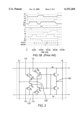
- FIG. 2 shows a schematic diagram of a switchable threshold sense amplifier according to an embodiment of the present invention
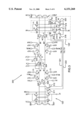
- FIG. 3 is a schematic diagram of a multilevel configuration for the sense amplifiers according to an embodiment of the present invention.
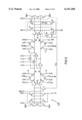
- FIG. 4 is a timing diagram for signals in circuitry of FIG. 3;
- FIG. 5 is a schematic diagram of reduced device count configuration
- FIGS. 6(a) and 6(b) show schematic diagrams of a parallel and a series configuration respectively.
- FIG. 7 is a schematic diagram of an A/D conversion circuit.
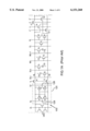
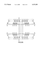
- FIGS. 1(a) and (b) a schematic diagram of a one half of a single column folded bitline of a multilevel DRAM and its associated timing diagram, according to the prior art is shown generally by numeral 100.
- N-channel pass transistors TC and TC* connect the left and right halves of the bitlines.
- L and R designates signals and devices to the left and right of the pass transistors respectively.
- Each bitline B and B* is divided into two equal sub-bitlines, BL, BR (not shown) and BL* and BR* (not shown) which are connected by the source drain circuits of the N channel pass transistors TC and TC* the gates of which are controlled by logic signals C and C* respectively.
- Diagonally opposite sub-bitlines are connected by the source drain circuit of N channel pass devices TX and TX* the gates of which are controlled by signals X and X*.
- Each of BL* and BL have respective cell capacitors CS connected thereto via the source drain circuit of a transistor TS. Although only one memory cell CS, TS is shown coupled to each sub-bitline it will be recognized that any number of cells may be coupled to each and they would be an array of columns.
- Each sub-bitline has a dummy memory cell capacitor CD connected thereto via the source drain circuit of an access transistor TD.
- the dummy cells match the storage cells now used to balance the capacitance seen in all sub-bitlines throughout the sense and restore operation. Odd and even dummy word lines DLo, DLe, DRo and DRe are normally enabled. Before a word line WLi or WLi+l is selected to enable an access transistor TS, the dummy word line on the corresponding sub-bitline is turned off.
- the pair of sub-bitlines on the left (BL, BL*) and on the right (BR, BR*) are connected via the source drain circuit of isolation transistors TI to sense amplifiers 120 and 122 (not shown) respectively by asserting the sense amplifier isolation signals IL and IR, respectively to isolation devices TI.
- the sense amplifier isolation devices TI also allow the sense amplifiers 120 and 122 (not shown) to be shared with adjacent arrays to save chip area.
- the sense amplifiers indicated by block 120 comprise a pair of N-channel devices N1 and N2 having their source-drain circuits connected in series between the bitlines BL and BL* and a pair of P channel devices P1 and P2 having their source-drain circuits connected in series between the bitlines BL and BL*.
- the junction 126 of the N channel transistors N1 and N2 and the P channel transistors P1 and P2 128, respectively is connected to a sense signal SL* and a restore signal RL respectively. These signals are normally held at V DD /2.
- a V PP level is defined as a voltage sufficiently high to turn on an N channel device having back bias and a source voltage equal to V DD .
- the sense amplifier comprises a pair of P channel transistors P1' and P2' having with their source drain circuits connected in series, the junction 126' of which is connected to a restore signal line RL'.
- the gate connections of P1' and P2' are connected to bitlines BL* and BL respectively.
- each of the gates of P1' and P2' is connected to the gates of a pair of serially connected N-channel pull down transistor N 1 ', N 3 ' and N 4 ', N 2 ' respectively.
- the junction 128' of their source-drain connection is connected to a sense signal SL'*.
- Each of the transistors N 1 ', N 3 ' and N 4 ', N 2 ' have their drains connected via the source-drain circuit of respective N-channel transistor N 6 ', N 5 ' and N 8 ', N 7 ' to bitlines BL and BL* respectively.
- the transistors N 6 ', N 5 ', N 8 ' and N 7 ' are selection switches which are enabled by selection signals TS1, TS0, TS2 and TS3 respectively.
- the present invention describes encoding two bits using a four-voltage-level-per-cell system, additional levels may be stored without changing the basic concepts of the invention. Similar to the prior art approach, described with reference to FIG. 1, folded bit lines are divided into sub-bit lines and two sense amplifiers per column are used to sense the two bits. However, instead of using complex, timing-sensitive charge sharing techniques between adjacent sub-bit lines to generate the reference voltage required to sense the second bit as described in the prior art, the present invention selectively enables sense amplifiers to operate at predetermined sensing thresholds, thereby greatly simplifying the sense and restore operations.
- the key to the invention is the addition of selective functionality to a typical common bit line sense amplifier. This is accomplished by the addition of specifically sized transistors to the standard bit line sense amplifier configuration to allow the intentional introduction of an imbalance in the sense amplifier-switching threshold.
- a typical sense amplifier of the prior art is designed to have its switching threshold at the half-VDD
- a sense amplifier according to the present invention can be effectively programmed to switch at other voltage levels, thus eliminating the need for the slow and complex generation of sensing reference levels during the active cycle.
- the differential sensing voltage AV is given by the general expression: ##EQU1## where V cell and C cell the cell voltage and capacitance, and V BLP and C BL are the bit line precharge voltage and bit line capacitance.
- V cell and C cell the cell voltage and capacitance
- V BLP and C BL are the bit line precharge voltage and bit line capacitance.
- C BL ⁇ 10C cell therefore, the above can be approximated to be:
- V BLP is 1.65V.
- V BLP is taken as the zero reference, then for the following V cell values and their binary configurations corresponding to the sign and magnitude information, the corresponding differential voltages will appear on the bit line for sensing:
- the sense amplifiers operate with voltage differences in the 50-100 mV range. For the four voltage levels stored in the cell, there are four corresponding voltages appearing on the bit lines to be sensed.
- the sign bit is sensed with respect to V REF2 i.e. 1/2 V DD .
- the magnitude bit is sensed either with respect to V REF1 or V REF3 .
- V REF1 or V REF3 must be generated as part of the active cycle and during the sensing period. This requires a time-consuming complex charge sharing scheme to be implemented.
- an imbalance is purposely introduced by varying the channel lengths and/or widths of the NMOS and/or PMOS transistors in the sense amplifier to allow it to properly sense these four differential voltage values.
- the effect of an imbalance in the component transistors results in an offset in the differential mode voltage.
- transistors N1' and N2' are inserted into the circuit as shown (alternately, PMOS additional transistors may be employed using the same concept, as shown later).
- transistors N5'-N8' represent selection switches to be enabled by the signals TSO*, TS3.
- transistors N3' and N4' for example, as well as the specific sizing of these two transistors along with specific sizing for N1' and N2', illustrate the main concept of the present invention.
- the switching threshold of the sense amplifier can be modified to emulate the two reference voltages which are generated in the prior art as part of an active sensing operation.
- transistors N1', N2', N3' and N4' have predetermined lengths L1, L2, L3 and L4 respectively.
- N3' Since N3' has a shorter gate length than N4', it will also have a smaller threshold voltage V t and will therefore turn ON for lower voltages applied to its gate. It is also important however, to keep in mind that while the N3', N5' NMOS transistor branch is conducting, the PMOS transistor P1' is also somewhat conductive. Therefore, in choosing the appropriate length of N3', the PMOS conduction of P1' must also be taken into consideration. The result will be a skewed inverter consisting of PMOS P1', NMOS N5', and N3' which will have a switching threshold at a point lower than V DD /2.
- the switching threshold of the inverter can also be adjusted upwards by enabling an NMOS transistor in the series path, for example, which has a higher V t and will therefore switch at higher voltage levels and will skew the inverter to a higher switching point.
- FIG. 3 a memory column for a multilevel DRAM implementation using the sense amplifier of FIG. 2 having left (BL, BL*) and right (BR, BR*) bitlines is shown generally by numeral 300.
- the circuit configuration is similar to the circuit shown in FIG. 1(a) also described in U.S. Pat. No. 5,612,912 incorporated herein by reference.
- the novel features have been numbered and will be described in detail thus similar reference characters will refer to corresponding signals and circuit elements.
- the novel features have been numbered accordingly and will be described in detail.
- Analogous control signals will be referred to by a prime character added to the corresponding reference character shown in FIG. 1(a).
- the right bitlines BR and BR* are connected via the source drain circuit of transistors T1 to sense amplifier circuit 120' of FIG. 2.
- a pair of feedback transistor F1 and F2 have their source drain circuits connected between the left bitlines BL*, BL and the gates of transistor N 8 ', N 5' and N 7' , N 6 ' respectively.
- the feedback transistors are controlled by a signal FBK connected to the gates.
- bitlines BL and bitlines BL* as well as bitlines BR and bitlines BR* are all precharged to V BLP through the left and right precharge devices driven by ZL and ZR respectively.
- ZL and ZR start out high.
- the isolation devices TI (325, 326) and (331, 332) controlled by IL and IR are also turned on during precharge, allowing a uniform precharge voltage across both left and right sub-bitlines.
- the isolation signals TI are both turned off at t 1 .
- the dummy word line DLL is switched off (low) and the selected word line on the left side, WLL i is enabled at t 2 .
- both left and right precharge signals ZL and ZR are disabled, the feedback signal FBK is also disabled in order to allow for sensing of the sign bit on the left side sense amplifier 120.
- the left/right coupling devices TC and TC* are turned off by the C and C* signals both being low.
- the left isolation signal IL enables the left side isolation devices TI (325, 326) once again, in order to allow the left sense amplifier 120 to sense the sign bit.
- the sense and restore power signals SL and RL for the left side are enabled and sensing of the sign bit occurs.
- the second portion of the sense operation involves sensing the magnitude bit using the information from the sensed sign bit.
- the feedback signal FBK is switched on to feed the sign bit information back to the magnitude bit sense amplifier 120'.
- bitlines BL is high for example, transistor F2 (312) (assuming WLL i has been selected) will pass this information to the magnitude sense amplifier 120' and turn on transistors N 8 ' (313) and N 5 ' (315).
- the magnitude information has been resting in the cell as well as on bitlines BR, since the coupling transistor TC (323) was not turned off until the data was also put onto bitlines BR.
- the actual data was at V cell2 voltage level, i.e.
- the present invention eliminates the need for the charge sharing step and reference voltage generation during sensing. Instead, by sizing the transistors N 1 '-N 8 ' in the magnitude sense amplifier 120' according to predetermined levels and by feeding back the sign bit information, the effect of generating the reference voltage of the prior art is emulated by offsetting the switching threshold of the magnitude sense amplifier. The sign bit therefore determines the magnitude threshold of the magnitude bit.
- the switching threshold of branch consisting of transistors N 4 ' (318), N 8 ' (313) and P 2 ' (327) will be shifted to a point 100 mV lower than that of the branch consisting of P' (328), N 5 ' (315), and N 3 ' (320).
- the data sitting on bitlines BR will then have to switch this offset threshold.
- the feedback signal may be turned off and the right side isolation devices are turned on in preparation of sensing the magnitude bit.
- the right side sense and restore power signals SR* and RR are enabled at t 8 . Since the threshold of branch N 4 ' (318), N 8 ' (313) and P2' (327) is 100 mV lower than that of the branch consisting of P 1 ' (328), N 5 ' (315), and N 3 ' (320), and since the data corresponding to the 1 0 configuration (approximately 50 mV according to Table 1b) is sitting on bitlines BR, the transistor branch N 4 ' (318), N 8 ' (313), P 2 ' (327) will pull bitlines BR low, and branch P 1 ' (328), N 5 ' (315) and N 3 ' (320) will pull bitlines BR* high. This last step completes the sensing of the magnitude bit.
- the selected word line WLLi is only activated once and therefore only one row activation path is necessary. This represents a substantial area savings over the prior art multi-level DRAM architecture.
- the right side isolation devices T1, (331, 332) are switched off.
- the cross-coupling transistor TX* (329) controlled by signal X* is turned on in order to accomplish a similar charge sharing effect as in the prior art restore.
- the left side isolation devices as also switched off and the coupling transistor 324 controlled by C* is switched on.
- bitlines BR, bitlines BL* and bitlines BR* are all shorted together, the charge sharing occurring completes the restore operation. Note once again that the word line was only activated once for both the sense and the restore.
- the ability therefore to switch the threshold of the sense amplifier on the fly during the sensing operation by selecting the transistor to be used for sensing allows multiple thresholds to be programmed into the circuit and, if constructed correctly, allow for multilevel sensing.
- FIG. 5 illustrates a reduced device count configuration for multilevel DRAM implementation.
- one of the NMOS pull down transistors N2' is set at the reference device width W, for example.
- Another design variation can address inaccuracies in the switching threshold adjustment caused by improper device sizing due to process variations and/or fluctuating operating voltages.
- a well or substrate connection for the switching threshold adjust devices will assist in maintaining the device performance more constant under such circumstances.
- FIG. 6a and FIG. 6b illustrate other possible configurations. All the series and parallel configurations are shown in these two general cases.
- the pass transistor shown may be N or P type.
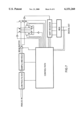
- FIG. 7 illustrates an embodiment of the present invention for A/D conversion with an array of sense amplifiers.
- Differential analog inputs are passed through a low pass filter and through a sample and hold circuit, both under the control of a main control circuit.
- the analog signals are then passed through a weak buffer, a non-inverting differential amplifier for example, and then input into a switching threshold adjustable sense amplifier according to an embodiment of the present invention.
- the gate control signals used to select the switching threshold are provided by the main control circuit.
- the output of the sense amplifier is inverted and then passed through a shift register and a multiplexer to the digital output.
- An array of such sense amplifier circuits can be arranged to cover various analog levels and inputs.
Abstract
Description
ΔV=(V.sub.cell -V.sub.BLP)/11
______________________________________
         Binary Configuration
Vcell   (sign)       (magnitude)
                               ΔV
______________________________________
3.3 V   1            1         150 mV
2.2 V   1            0          50 mV
1.1 V   0            1         -50 mV
  0 V   0            0         -150 mV
______________________________________
______________________________________
Storage Voltages
             Reference Voltages
                          Actual Voltages
______________________________________
V.sub.cell3               V.sub.DD
             V.sub.REF3   5/6 V.sub.DD
V.sub.cell2               2/3 V.sub.DD
             V.sub.REF2   1/2 V.sub.DD
V.sub.cell1               1/3 V.sub.DD
             V.sub.REF1   1/6 V.sub.DD
V.sub.cell0               V.sub.SS
______________________________________
Claims (5)
Priority Applications (4)
| Application Number | Priority Date | Filing Date | Title |
|---|---|---|---|
| US09/585,791 US6373766B1 (en) | 1997-09-30 | 2000-06-05 | Multilevel DRAM sense amplifier |
| US09/585,790 US6373765B1 (en) | 1997-09-30 | 2000-06-05 | Method for multilevel DRAM sensing |
| US10/118,338 US6625075B2 (en) | 1997-09-30 | 2002-04-09 | Multilevel DRAM sensing analog-to-digital converter |
| US10/640,305 US20040032785A1 (en) | 1997-09-30 | 2003-08-14 | Method for multilevel DRAM sensing |
Applications Claiming Priority (2)
| Application Number | Priority Date | Filing Date | Title |
|---|---|---|---|
| CA002217359A CA2217359C (en) | 1997-09-30 | 1997-09-30 | Method for multilevel dram sensing |
| CA2-217-359 | 1997-09-30 |
Related Child Applications (2)
| Application Number | Title | Priority Date | Filing Date |
|---|---|---|---|
| US09/585,790 Continuation US6373765B1 (en) | 1997-09-30 | 2000-06-05 | Method for multilevel DRAM sensing |
| US09/585,791 Division US6373766B1 (en) | 1997-09-30 | 2000-06-05 | Multilevel DRAM sense amplifier |
Publications (1)
| Publication Number | Publication Date |
|---|---|
| US6151260A true US6151260A (en) | 2000-11-21 |
Family
ID=4161576
Family Applications (5)
| Application Number | Title | Priority Date | Filing Date |
|---|---|---|---|
| US09/046,636 Expired - Lifetime US6151260A (en) | 1997-09-30 | 1998-03-24 | Method for multilevel DRAM sensing |
| US09/585,790 Expired - Lifetime US6373765B1 (en) | 1997-09-30 | 2000-06-05 | Method for multilevel DRAM sensing |
| US09/585,791 Expired - Lifetime US6373766B1 (en) | 1997-09-30 | 2000-06-05 | Multilevel DRAM sense amplifier |
| US10/118,338 Expired - Fee Related US6625075B2 (en) | 1997-09-30 | 2002-04-09 | Multilevel DRAM sensing analog-to-digital converter |
| US10/640,305 Abandoned US20040032785A1 (en) | 1997-09-30 | 2003-08-14 | Method for multilevel DRAM sensing |
Family Applications After (4)
| Application Number | Title | Priority Date | Filing Date |
|---|---|---|---|
| US09/585,790 Expired - Lifetime US6373765B1 (en) | 1997-09-30 | 2000-06-05 | Method for multilevel DRAM sensing |
| US09/585,791 Expired - Lifetime US6373766B1 (en) | 1997-09-30 | 2000-06-05 | Multilevel DRAM sense amplifier |
| US10/118,338 Expired - Fee Related US6625075B2 (en) | 1997-09-30 | 2002-04-09 | Multilevel DRAM sensing analog-to-digital converter |
| US10/640,305 Abandoned US20040032785A1 (en) | 1997-09-30 | 2003-08-14 | Method for multilevel DRAM sensing |
Country Status (2)
| Country | Link |
|---|---|
| US (5) | US6151260A (en) |
| CA (1) | CA2217359C (en) |
Cited By (16)
| Publication number | Priority date | Publication date | Assignee | Title |
|---|---|---|---|---|
| US6373765B1 (en) * | 1997-09-30 | 2002-04-16 | Mosaid Technologies Incorporated | Method for multilevel DRAM sensing |
| US6519174B2 (en) | 2001-05-16 | 2003-02-11 | International Business Machines Corporation | Early write DRAM architecture with vertically folded bitlines |
| US6556469B2 (en) * | 1999-05-26 | 2003-04-29 | Gershom Birk | System and method for multilevel DRAM sensing and restoring |
| US7046565B1 (en) | 2005-02-22 | 2006-05-16 | International Business Machines Corporation | Bi-mode sense amplifier with dual utilization of the reference cells and dual precharge scheme for improving data retention |
| US20130100723A1 (en) * | 2011-10-24 | 2013-04-25 | Semiconductor Energy Laboratory Co., Ltd. | Semiconductor memory device and driving method thereof |
| US8773925B2 (en) | 2010-02-23 | 2014-07-08 | Rambus Inc. | Multilevel DRAM |
| US20140292307A1 (en) * | 2011-06-14 | 2014-10-02 | Infineon Technologies Ag | DC Decoupled Current Measurement |
| US9478277B1 (en) * | 2015-09-03 | 2016-10-25 | Bo Liu | Tri-level-cell DRAM and sense amplifier with alternating offset voltage |
| US9660024B2 (en) | 2014-12-18 | 2017-05-23 | Samsung Electronics Co., Ltd. | Semiconductor device with two transistors and a capacitor |
| US9704571B2 (en) | 2015-08-11 | 2017-07-11 | Samsung Electronics Co., Ltd. | Memory device and a method of operating the same |
| US9978441B2 (en) | 2016-09-20 | 2018-05-22 | Toshiba Memory Corporation | Semiconductor memory device |
| US20180277177A1 (en) * | 2017-03-22 | 2018-09-27 | Toshiba Memory Corporation | Memory device and memory system |
| US10236053B1 (en) | 2017-10-17 | 2019-03-19 | R&D 3 Llc | Method and circuit device incorporating time-to-transition signal node sensing |
| US10497428B2 (en) | 2017-12-18 | 2019-12-03 | Samsung Electronics Co., Ltd. | Bit line sense amplifier, semiconductor memory device and multi bit data sensing method thereof |
| US10706911B1 (en) | 2018-10-10 | 2020-07-07 | Samsung Electronics Co., Ltd. | Sense amplifier for sensing multi-level cell and memory device including the sense amplifier |
| US11501826B2 (en) | 2017-10-17 | 2022-11-15 | R&D3 Llc | Memory device having variable impedance memory cells and time-to-transition sensing of data stored therein |
Families Citing this family (9)
| Publication number | Priority date | Publication date | Assignee | Title |
|---|---|---|---|---|
| US20030235089A1 (en) * | 2002-04-02 | 2003-12-25 | Gerhard Mueller | Memory array with diagonal bitlines |
| KR100518230B1 (en) * | 2003-06-16 | 2005-10-04 | 주식회사 하이닉스반도체 | A driving voltage driver for sense amplifier of memory device |
| US20070069172A1 (en) * | 2005-04-26 | 2007-03-29 | Parker-Hannifin Corporation | Magnetic repulsion actuator and method |
| US7330388B1 (en) * | 2005-09-23 | 2008-02-12 | Cypress Semiconductor Corporation | Sense amplifier circuit and method of operation |
| WO2007063264A1 (en) * | 2005-12-02 | 2007-06-07 | Arm Limited | Data processing system |
| US7606097B2 (en) * | 2006-12-27 | 2009-10-20 | Micron Technology, Inc. | Array sense amplifiers, memory devices and systems including same, and methods of operation |
| US9905276B2 (en) * | 2015-12-21 | 2018-02-27 | Micron Technology, Inc. | Control of sensing components in association with performing operations |
| KR102471418B1 (en) * | 2018-05-23 | 2022-11-29 | 에스케이하이닉스 주식회사 | Sensing circuit and semiconductor device including the same |
| US11024365B1 (en) | 2020-02-05 | 2021-06-01 | Samsung Electronics Co., Ltd. | Time interleaved sampling of sense amplifier circuits, memory devices and methods of operating memory devices |
Citations (6)
| Publication number | Priority date | Publication date | Assignee | Title |
|---|---|---|---|---|
| US4608670A (en) * | 1984-08-02 | 1986-08-26 | Texas Instruments Incorporated | CMOS sense amplifier with N-channel sensing |
| US4841483A (en) * | 1986-12-15 | 1989-06-20 | Kabushiki Kaisha Toshiba | Semiconductor memory |
| US5119330A (en) * | 1989-03-31 | 1992-06-02 | Oki Electric Industry Co, Ltd. | Nonvolatile memory system for multiple value storing |
| US5532955A (en) * | 1994-12-30 | 1996-07-02 | Mosaid Technologies Incorporated | Method of multilevel dram sense and restore |
| US5646900A (en) * | 1995-01-12 | 1997-07-08 | Mitsubishi Denki Kabushiki Kaisha | Sense amplifier including MOS transistors having threshold voltages controlled dynamically in a semiconductor memory device |
| US5701268A (en) * | 1995-08-23 | 1997-12-23 | Samsung Electronics Co., Ltd. | Sense amplifier for integrated circuit memory devices having boosted sense and current drive capability and methods of operating same |
Family Cites Families (6)
| Publication number | Priority date | Publication date | Assignee | Title |
|---|---|---|---|---|
| JPH08195083A (en) * | 1995-01-17 | 1996-07-30 | Toshiba Microelectron Corp | Semiconductor memory |
| JP3607407B2 (en) * | 1995-04-26 | 2005-01-05 | 株式会社日立製作所 | Semiconductor memory device |
| JP4035194B2 (en) * | 1996-03-13 | 2008-01-16 | キヤノン株式会社 | X-ray detection apparatus and X-ray detection system |
| US5973957A (en) * | 1997-09-16 | 1999-10-26 | Intel Corporation | Sense amplifier comprising a preamplifier and a differential input latch for flash memories |
| CA2217359C (en) | 1997-09-30 | 2005-04-12 | Mosaid Technologies Incorporated | Method for multilevel dram sensing |
| US6208542B1 (en) * | 1998-06-30 | 2001-03-27 | Sandisk Corporation | Techniques for storing digital data in an analog or multilevel memory |
-
1997
- 1997-09-30 CA CA002217359A patent/CA2217359C/en not_active Expired - Fee Related
-
1998
- 1998-03-24 US US09/046,636 patent/US6151260A/en not_active Expired - Lifetime
-
2000
- 2000-06-05 US US09/585,790 patent/US6373765B1/en not_active Expired - Lifetime
- 2000-06-05 US US09/585,791 patent/US6373766B1/en not_active Expired - Lifetime
-
2002
- 2002-04-09 US US10/118,338 patent/US6625075B2/en not_active Expired - Fee Related
-
2003
- 2003-08-14 US US10/640,305 patent/US20040032785A1/en not_active Abandoned
Patent Citations (7)
| Publication number | Priority date | Publication date | Assignee | Title |
|---|---|---|---|---|
| US4608670A (en) * | 1984-08-02 | 1986-08-26 | Texas Instruments Incorporated | CMOS sense amplifier with N-channel sensing |
| US4841483A (en) * | 1986-12-15 | 1989-06-20 | Kabushiki Kaisha Toshiba | Semiconductor memory |
| US5119330A (en) * | 1989-03-31 | 1992-06-02 | Oki Electric Industry Co, Ltd. | Nonvolatile memory system for multiple value storing |
| US5532955A (en) * | 1994-12-30 | 1996-07-02 | Mosaid Technologies Incorporated | Method of multilevel dram sense and restore |
| US5612912A (en) * | 1994-12-30 | 1997-03-18 | Mosaid Technologies Incorporated | Method of multilevel DRAM sense and restore |
| US5646900A (en) * | 1995-01-12 | 1997-07-08 | Mitsubishi Denki Kabushiki Kaisha | Sense amplifier including MOS transistors having threshold voltages controlled dynamically in a semiconductor memory device |
| US5701268A (en) * | 1995-08-23 | 1997-12-23 | Samsung Electronics Co., Ltd. | Sense amplifier for integrated circuit memory devices having boosted sense and current drive capability and methods of operating same |
Non-Patent Citations (2)
| Title |
|---|
| A Sense and Restore Technique for Multilevel DRAM , Peter Gillingham, Jul. 1996, pp. 483 486. * |
| A Sense and Restore Technique for Multilevel DRAM, Peter Gillingham, Jul. 1996, pp. 483-486. |
Cited By (36)
| Publication number | Priority date | Publication date | Assignee | Title |
|---|---|---|---|---|
| US6625075B2 (en) | 1997-09-30 | 2003-09-23 | Gershom Birk | Multilevel DRAM sensing analog-to-digital converter |
| US20040032785A1 (en) * | 1997-09-30 | 2004-02-19 | Gershom Birk | Method for multilevel DRAM sensing |
| US6373765B1 (en) * | 1997-09-30 | 2002-04-16 | Mosaid Technologies Incorporated | Method for multilevel DRAM sensing |
| US6556469B2 (en) * | 1999-05-26 | 2003-04-29 | Gershom Birk | System and method for multilevel DRAM sensing and restoring |
| US6519174B2 (en) | 2001-05-16 | 2003-02-11 | International Business Machines Corporation | Early write DRAM architecture with vertically folded bitlines |
| US7046565B1 (en) | 2005-02-22 | 2006-05-16 | International Business Machines Corporation | Bi-mode sense amplifier with dual utilization of the reference cells and dual precharge scheme for improving data retention |
| US8773925B2 (en) | 2010-02-23 | 2014-07-08 | Rambus Inc. | Multilevel DRAM |
| US20140292307A1 (en) * | 2011-06-14 | 2014-10-02 | Infineon Technologies Ag | DC Decoupled Current Measurement |
| US9594097B2 (en) * | 2011-06-14 | 2017-03-14 | Infineon Technologies Ag | DC decoupled current measurement |
| TWI607434B (en) * | 2011-10-24 | 2017-12-01 | 半導體能源研究所股份有限公司 | Semiconductor memory device and driving method thereof |
| US9336836B2 (en) | 2011-10-24 | 2016-05-10 | Semiconductor Energy Laboratory Co., Ltd. | Semiconductor memory device and driving method thereof |
| US8913419B2 (en) * | 2011-10-24 | 2014-12-16 | Semiconductor Energy Laboratory Co., Ltd. | Semiconductor memory device and driving method thereof |
| KR102054018B1 (en) | 2011-10-24 | 2019-12-09 | 가부시키가이샤 한도오따이 에네루기 켄큐쇼 | Semiconductor memory device |
| KR20130045191A (en) * | 2011-10-24 | 2013-05-03 | 가부시키가이샤 한도오따이 에네루기 켄큐쇼 | Semiconductor memory device and driving method thereof |
| US20130100723A1 (en) * | 2011-10-24 | 2013-04-25 | Semiconductor Energy Laboratory Co., Ltd. | Semiconductor memory device and driving method thereof |
| US9660024B2 (en) | 2014-12-18 | 2017-05-23 | Samsung Electronics Co., Ltd. | Semiconductor device with two transistors and a capacitor |
| US9704571B2 (en) | 2015-08-11 | 2017-07-11 | Samsung Electronics Co., Ltd. | Memory device and a method of operating the same |
| CN106409328A (en) * | 2015-09-03 | 2017-02-15 | 深圳星忆存储科技有限公司 | Dynamic random access memory for three-level unit, and method for reading same |
| TWI576840B (en) * | 2015-09-03 | 2017-04-01 | 深圳星憶存儲科技有限公司 | Tri-level-cell dram and method for reading out the same |
| CN106409328B (en) * | 2015-09-03 | 2018-05-18 | 深圳星忆存储科技有限公司 | The dynamic random access memory and its read method of three-level cells |
| US9478277B1 (en) * | 2015-09-03 | 2016-10-25 | Bo Liu | Tri-level-cell DRAM and sense amplifier with alternating offset voltage |
| US9978441B2 (en) | 2016-09-20 | 2018-05-22 | Toshiba Memory Corporation | Semiconductor memory device |
| US20180277177A1 (en) * | 2017-03-22 | 2018-09-27 | Toshiba Memory Corporation | Memory device and memory system |
| US10249352B2 (en) * | 2017-03-22 | 2019-04-02 | Toshiba Memory Corporation | Memory device and memory system |
| US10236053B1 (en) | 2017-10-17 | 2019-03-19 | R&D 3 Llc | Method and circuit device incorporating time-to-transition signal node sensing |
| US10269413B1 (en) | 2017-10-17 | 2019-04-23 | R&D 3 Llc | Memory device having variable impedance memory cells and time-to-transition sensing of data stored therein |
| US10629256B2 (en) | 2017-10-17 | 2020-04-21 | R&D 3 Llc | Memory device having variable impedance memory cells and time-to-transition sensing of data stored therein |
| US10796748B2 (en) | 2017-10-17 | 2020-10-06 | R&D 3 Llc | Method and circuit device incorporating time-to-transition signal node sensing |
| US10796749B2 (en) | 2017-10-17 | 2020-10-06 | R&D 3 Llc | Memory device having variable impedance memory cells and time-to-transition sensing of data stored therein |
| US11049553B2 (en) | 2017-10-17 | 2021-06-29 | R&D 3 Llc | Memory device having variable impedance memory cells and time-to-transition sensing of data stored therein |
| US11195574B2 (en) | 2017-10-17 | 2021-12-07 | R&D 3 Llc | Memory device having variable impedance memory cells and time-to-transition sensing of data stored therein |
| US11501826B2 (en) | 2017-10-17 | 2022-11-15 | R&D3 Llc | Memory device having variable impedance memory cells and time-to-transition sensing of data stored therein |
| US11783891B2 (en) | 2017-10-17 | 2023-10-10 | R&D 3 Llc | Memory device having variable impedance memory cells and time-to-transition sensing of data stored therein |
| US10497428B2 (en) | 2017-12-18 | 2019-12-03 | Samsung Electronics Co., Ltd. | Bit line sense amplifier, semiconductor memory device and multi bit data sensing method thereof |
| US10706911B1 (en) | 2018-10-10 | 2020-07-07 | Samsung Electronics Co., Ltd. | Sense amplifier for sensing multi-level cell and memory device including the sense amplifier |
| US10854277B2 (en) | 2018-10-10 | 2020-12-01 | Samsung Electronics Co., Ltd. | Sense amplifier for sensing multi-level cell and memory device including the sense amplifer |
Also Published As
| Publication number | Publication date |
|---|---|
| CA2217359A1 (en) | 1999-03-30 |
| US6373765B1 (en) | 2002-04-16 |
| US20040032785A1 (en) | 2004-02-19 |
| US6373766B1 (en) | 2002-04-16 |
| US20020181306A1 (en) | 2002-12-05 |
| US6625075B2 (en) | 2003-09-23 |
| CA2217359C (en) | 2005-04-12 |
Similar Documents
| Publication | Publication Date | Title |
|---|---|---|
| US6151260A (en) | Method for multilevel DRAM sensing | |
| US5612912A (en) | Method of multilevel DRAM sense and restore | |
| US6034885A (en) | Multilevel memory cell sense amplifier system and sensing methods | |
| EP0643393B1 (en) | Semiconductor memory device having voltage booster circuit | |
| US9478277B1 (en) | Tri-level-cell DRAM and sense amplifier with alternating offset voltage | |
| US4965767A (en) | Associative memory having simplified memory cell circuitry | |
| US5276649A (en) | Dynamic-type semiconductor memory device having staggered activation of column groups | |
| US4841483A (en) | Semiconductor memory | |
| EP0278155B1 (en) | Dynamic random access memory | |
| US4627033A (en) | Sense amplifier with reduced instantaneous power | |
| EP0163951B1 (en) | Dynamic ram | |
| US5475642A (en) | Dynamic random access memory with bit line preamp/driver | |
| EP1433179B1 (en) | System and method for early write to memory by holding bitline at fixed potential | |
| US5625588A (en) | Single-ended sensing using global bit lines for DRAM | |
| US4980862A (en) | Folded bitline dynamic ram with reduced shared supply voltages | |
| US4982370A (en) | Shared sense amplifier semiconductor memory | |
| US5771187A (en) | Multiple level storage DRAM cell | |
| US6166977A (en) | Address controlled sense amplifier overdrive timing for semiconductor memory device | |
| US5303196A (en) | Open bit line memory devices and operational method | |
| EP0886865B1 (en) | Cell plate referencing for dram sensing | |
| KR20010010653A (en) | Sensing amp of nonvolatile ferroelectric memory device | |
| US6490211B2 (en) | Random access memory device | |
| US6643214B2 (en) | Semiconductor memory device having write column select gate | |
| JPH08180688A (en) | Semiconductor memory | |
| US7161863B2 (en) | DRAM refreshment |
Legal Events
| Date | Code | Title | Description |
|---|---|---|---|
| AS | Assignment |
Owner name: MOSAID TECHNOLOGIES INCORPORATED, CANADA Free format text: ASSIGNMENT OF ASSIGNORS INTEREST;ASSIGNOR:BIRK, GERSHOM;REEL/FRAME:009265/0069 Effective date: 19971218 |
|
| STCF | Information on status: patent grant |
Free format text: PATENTED CASE |
|
| FPAY | Fee payment |
Year of fee payment: 4 |
|
| FEPP | Fee payment procedure |
Free format text: PAYOR NUMBER ASSIGNED (ORIGINAL EVENT CODE: ASPN); ENTITY STATUS OF PATENT OWNER: LARGE ENTITY |
|
| FEPP | Fee payment procedure |
Free format text: PAYOR NUMBER ASSIGNED (ORIGINAL EVENT CODE: ASPN); ENTITY STATUS OF PATENT OWNER: LARGE ENTITY Free format text: PAYER NUMBER DE-ASSIGNED (ORIGINAL EVENT CODE: RMPN); ENTITY STATUS OF PATENT OWNER: LARGE ENTITY |
|
| FPAY | Fee payment |
Year of fee payment: 8 |
|
| AS | Assignment |
Owner name: MOSAID TECHNOLOGIES INCORPORATED, CANADA Free format text: CHANGE OF ADDRESS;ASSIGNOR:MOSAID TECHNOLOGIES INCORPORATED;REEL/FRAME:025346/0803 Effective date: 20090209 Owner name: MOSAID TECHNOLOGIES INCORPORATED, CANADA Free format text: CORRECTION OF NAME AND ADDRESS;ASSIGNOR:MOSAID TECHNOLOGIES INCORPORATED;REEL/FRAME:025346/0795 Effective date: 20090917 |
|
| AS | Assignment |
Owner name: ROYAL BANK OF CANADA, CANADA Free format text: U.S. INTELLECTUAL PROPERTY SECURITY AGREEMENT (FOR NON-U.S. GRANTORS) - SHORT FORM;ASSIGNORS:658276 N.B. LTD.;658868 N.B. INC.;MOSAID TECHNOLOGIES INCORPORATED;REEL/FRAME:027512/0196 Effective date: 20111223 |
|
| FPAY | Fee payment |
Year of fee payment: 12 |
|
| AS | Assignment |
Owner name: CONVERSANT INTELLECTUAL PROPERTY MANAGEMENT INC., Free format text: CHANGE OF NAME;ASSIGNOR:MOSAID TECHNOLOGIES INCORPORATED;REEL/FRAME:032439/0638 Effective date: 20140101 |
|
| AS | Assignment |
Owner name: CONVERSANT IP N.B. 868 INC., CANADA Free format text: RELEASE OF SECURITY INTEREST;ASSIGNOR:ROYAL BANK OF CANADA;REEL/FRAME:033484/0344 Effective date: 20140611 Owner name: CONVERSANT IP N.B. 276 INC., CANADA Free format text: RELEASE OF SECURITY INTEREST;ASSIGNOR:ROYAL BANK OF CANADA;REEL/FRAME:033484/0344 Effective date: 20140611 Owner name: CONVERSANT INTELLECTUAL PROPERTY MANAGEMENT INC., Free format text: RELEASE OF SECURITY INTEREST;ASSIGNOR:ROYAL BANK OF CANADA;REEL/FRAME:033484/0344 Effective date: 20140611 |
|
| AS | Assignment |
Owner name: CONVERSANT INTELLECTUAL PROPERTY MANAGEMENT INC., CANADA Free format text: CHANGE OF ADDRESS;ASSIGNOR:CONVERSANT INTELLECTUAL PROPERTY MANAGEMENT INC.;REEL/FRAME:033678/0096 Effective date: 20140820 Owner name: CONVERSANT INTELLECTUAL PROPERTY MANAGEMENT INC., Free format text: CHANGE OF ADDRESS;ASSIGNOR:CONVERSANT INTELLECTUAL PROPERTY MANAGEMENT INC.;REEL/FRAME:033678/0096 Effective date: 20140820 |
|
| AS | Assignment |
Owner name: ROYAL BANK OF CANADA, AS LENDER, CANADA Free format text: U.S. PATENT SECURITY AGREEMENT (FOR NON-U.S. GRANTORS);ASSIGNOR:CONVERSANT INTELLECTUAL PROPERTY MANAGEMENT INC.;REEL/FRAME:033706/0367 Effective date: 20140611 Owner name: CPPIB CREDIT INVESTMENTS INC., AS LENDER, CANADA Free format text: U.S. PATENT SECURITY AGREEMENT (FOR NON-U.S. GRANTORS);ASSIGNOR:CONVERSANT INTELLECTUAL PROPERTY MANAGEMENT INC.;REEL/FRAME:033706/0367 Effective date: 20140611 |
|
| AS | Assignment |
Owner name: CONVERSANT INTELLECTUAL PROPERTY MANAGEMENT INC., CANADA Free format text: RELEASE OF U.S. PATENT AGREEMENT (FOR NON-U.S. GRANTORS);ASSIGNOR:ROYAL BANK OF CANADA, AS LENDER;REEL/FRAME:047645/0424 Effective date: 20180731 Owner name: CONVERSANT INTELLECTUAL PROPERTY MANAGEMENT INC., Free format text: RELEASE OF U.S. PATENT AGREEMENT (FOR NON-U.S. GRANTORS);ASSIGNOR:ROYAL BANK OF CANADA, AS LENDER;REEL/FRAME:047645/0424 Effective date: 20180731 |