US6207263B1 - Anti-reflection film and process for preparation thereof - Google Patents

Anti-reflection film and process for preparation thereof Download PDF

Info

Publication number
US6207263B1
US6207263B1 US09/007,796 US779698A US6207263B1 US 6207263 B1 US6207263 B1 US 6207263B1 US 779698 A US779698 A US 779698A US 6207263 B1 US6207263 B1 US 6207263B1
Authority
US
United States
Prior art keywords
refractive index
index layer
layer
reflection film
film
Prior art date
Legal status (The legal status is an assumption and is not a legal conclusion. Google has not performed a legal analysis and makes no representation as to the accuracy of the status listed.)
Expired - Lifetime
Application number
US09/007,796
Inventor
Kiyotaka Takematsu
Hiroomi Katagiri
Current Assignee (The listed assignees may be inaccurate. Google has not performed a legal analysis and makes no representation or warranty as to the accuracy of the list.)
Dai Nippon Printing Co Ltd
Original Assignee
Dai Nippon Printing Co Ltd
Priority date (The priority date is an assumption and is not a legal conclusion. Google has not performed a legal analysis and makes no representation as to the accuracy of the date listed.)
Filing date
Publication date
Application filed by Dai Nippon Printing Co Ltd filed Critical Dai Nippon Printing Co Ltd
Assigned to DAI NIPPON PRINTING CO., LTD. reassignment DAI NIPPON PRINTING CO., LTD. ASSIGNMENT OF ASSIGNORS INTEREST (SEE DOCUMENT FOR DETAILS). Assignors: KATAGIRI, HIROOMI, TAKEMATSU, KIYOTAKA
Priority to US09/754,130 priority Critical patent/US20010021446A1/en
Application granted granted Critical
Publication of US6207263B1 publication Critical patent/US6207263B1/en
Anticipated expiration legal-status Critical
Expired - Lifetime legal-status Critical Current

Links

Images

Classifications

    • GPHYSICS
    • G02OPTICS
    • G02BOPTICAL ELEMENTS, SYSTEMS OR APPARATUS
    • G02B1/00Optical elements characterised by the material of which they are made; Optical coatings for optical elements
    • G02B1/10Optical coatings produced by application to, or surface treatment of, optical elements
    • G02B1/11Anti-reflection coatings
    • G02B1/113Anti-reflection coatings using inorganic layer materials only
    • YGENERAL TAGGING OF NEW TECHNOLOGICAL DEVELOPMENTS; GENERAL TAGGING OF CROSS-SECTIONAL TECHNOLOGIES SPANNING OVER SEVERAL SECTIONS OF THE IPC; TECHNICAL SUBJECTS COVERED BY FORMER USPC CROSS-REFERENCE ART COLLECTIONS [XRACs] AND DIGESTS
    • Y10TECHNICAL SUBJECTS COVERED BY FORMER USPC
    • Y10TTECHNICAL SUBJECTS COVERED BY FORMER US CLASSIFICATION
    • Y10T428/00Stock material or miscellaneous articles
    • Y10T428/24Structurally defined web or sheet [e.g., overall dimension, etc.]
    • Y10T428/24355Continuous and nonuniform or irregular surface on layer or component [e.g., roofing, etc.]
    • Y10T428/24364Continuous and nonuniform or irregular surface on layer or component [e.g., roofing, etc.] with transparent or protective coating
    • YGENERAL TAGGING OF NEW TECHNOLOGICAL DEVELOPMENTS; GENERAL TAGGING OF CROSS-SECTIONAL TECHNOLOGIES SPANNING OVER SEVERAL SECTIONS OF THE IPC; TECHNICAL SUBJECTS COVERED BY FORMER USPC CROSS-REFERENCE ART COLLECTIONS [XRACs] AND DIGESTS
    • Y10TECHNICAL SUBJECTS COVERED BY FORMER USPC
    • Y10TTECHNICAL SUBJECTS COVERED BY FORMER US CLASSIFICATION
    • Y10T428/00Stock material or miscellaneous articles
    • Y10T428/24Structurally defined web or sheet [e.g., overall dimension, etc.]
    • Y10T428/24942Structurally defined web or sheet [e.g., overall dimension, etc.] including components having same physical characteristic in differing degree
    • Y10T428/2495Thickness [relative or absolute]

Definitions

  • the present invention relates to a film having optical functions such as anti-glare properties. More specifically, the invention relates to a film with excellent optical characteristics which is suitable as an anti-reflection film on the surface of various displays of word processors, computers and TV sets, polarizing plates for use in liquid crystal display devices, lenses of sunglasses composed of transparent plastics, lenses of vision-correcting eyeglasses, optical lenses such as camera finder lenses, covers for various gauges, and window glasses of automobiles and electric trains.
  • Transparent base plates of glass, plastic or the like are used for displays of curve mirrors, rear view mirrors, goggles, window glasses, displays for personal computers and word processors, and various other displays for commercial use.
  • Techniques for preventing the reflection of light include a method of coating an anti-reflection coating on the surface of a glass or plastic material, a method of providing a super thin film of MgF 2 or the like or a vacuum deposited metal film about 0.1 ⁇ m thick on the surface of a transparent base plate of glass or the like, a method of coating an ionizing radiation curing resin on the surface of a plastic lens and forming a film of SiO x or MgF 2 on the coating by vacuum deposition, and a method of further forming a coating with a low refractive index on a cured film of an ionizing radiation curing resin.
  • Equation 1 tells that an effective way of preventing reflection of light 100% is to select a material in which the refractive index of a coating on the upper layer side is close to the square root of the refractive index of the lower layer laid under the coating.
  • An object of the present invention is to provide an anti-reflection film for use in a display in which the surface of a transparent base plate prevents the reflection of light and transmits necessary visual information inside the transparent base plate, and enables an observer to clearly discern the visual information, when seeing objects or visual information, such as characters or graphics, through the transparent base plate, or observing an image from a reflection layer through the transparent base plate of a mirror.
  • the invention for attaining this object resides in an anti-reflection film 10 having an intermediate refractive index layer 3 , a high refractive index layer 2 and a low refractive index layer 1 formed in this sequence on a transparent base film 5 via a hard coat layer 4 , the anti-reflection film 10 comprising:
  • the low refractive index layer 1 comprising an SiO x layer
  • the intermediate refractive index layer 3 constituted by a coating of a composition comprising a binder and ultrafine particles having a refractive index of 1.5 or more;
  • the high refractive index layer 2 having electric conductivity
  • the anti-reflection film 10 having:
  • each refractive index layer being 80 to 110 nm for the low refractive index layer, 30 to 110 nm for the high refractive index layer, and 50 to 100 nm for the intermediate refractive index layer;
  • the anti-reflection film 10 is such that the hard coat layer 4 has irregularities on its surface in contact with the intermediate refractive index layer 3 , and the hard coat layer 4 is provided on the transparent base film 5 directly or via a primer layer 7 and/or an adhesive layer 9 , as illustrated in FIG. 6 .
  • the anti-reflection film 10 is such that the intermediate refractive index layer is composed of 0.1 to 20 parts by weight of a mat material based on one part by weight of a thermosetting resin and/or an ionizing radiation curing resin, the mat material being selected from fine particles of one or more kinds selected from the group consisting of ultrafine particles of ZnO, TiO 2 , CeO 2 , Sb 2 O 5 , SnO 2 , ITO, Y 2 O 3 , La 2 O 3 , Al 2 O 3 , Hf 2 O 3 and ZrO 2 .
  • the anti-reflection film 10 is such that the high refractive index layer and the low refractive index layer are each a layer provided by vacuum coating.
  • the anti-reflection film 10 is such that the low refractive index layer is formed by plasma CVD involving the discharge of the starting gas of an organosiloxane, and the undecomposed organosiloxane remains in an amount of 0.1 to 0.2 part based on the SiO X .
  • an antifouling layer may be formed on the low refractive index layer.
  • a first process for preparation of the anti-reflection film of the present invention is as follows:
  • an uncured hard coat layer 46 of the curing reaction type is provided on a transparent base film 5 .
  • an uncured intermediate refractive index layer 36 comprising a composition containing a binder and fine particles having a higher refractive index than the refractive index of the binder is coated on the transparent base film.
  • a laminate having a finely irregular, matted shaped film 6 laminated and shaped on the uncured hard coat layer and intermediate refractive index layer (see FIG. 3A) is heat-treated and/or ionizing radiation treated to cure the hard coat layer and intermediate refractive index layer.
  • the shaped film 6 H is stripped off to form an intermediate refractive index layer 3 having irregularities on the surface of a hard coat layer 4 as illustrated in FIG. 3 B.
  • a high refractive index layer 2 is formed by vacuum deposition or sputtering. Further, a low refractive index layer 1 comprising an SiO x layer is formed by vacuum deposition, sputtering or plasma CVD to constitute an anti-reflection film 10 . This is shown in FIG. 3 C.
  • a second process for preparation of the anti-reflection film of the invention is as follows:
  • a matted shaped film 6 having irregularities on the surface is coated with an uncured intermediate refractive index layer 36 comprising a composition containing a binder and fine particles having a higher refractive index than the refractive index of the binder.
  • an uncured hard coat layer 46 provided on a transparent base film 5 is laminated as shown in FIG. 4 A.
  • the resulting laminate is heat-treated and/or ionizing radiation treated to cure the intermediate refractive index layer and hard coat layer.
  • the shaped film 6 H is stripped off to form an intermediate refractive index layer 3 having irregularities on the surface of a hard coat layer 4 (see FIG. 4 B).
  • a high refractive index layer 2 and a low refractive index layer 1 are laminated and formed in the same manner as in the first preparation process.
  • an antifouling coat layer 42 may be formed on the low refractive index layer.
  • a third process for preparation of the anti-reflection film of the invention is as follows:
  • a shaped film 6 is coated with an uncured intermediate refractive index layer containing a binder and fine particles having a higher refractive index than the refractive index of the binder, and an uncured hard coat layer. Then, the uncured layers are cured.
  • a transparent base film is coated with a reactive adhesive layer 9 .
  • the cured intermediate refractive index layer is laminated.
  • the resulting laminate is heat-treated and/or ionizing radiation treated to cure the adhesive layer to prepare a laminate as shown in FIG. 5 B.
  • the shaped film 6 H is stripped off to form an intermediate refractive index layer 3 on a transparent base film 5 via the adhesive layer 9 and the hard coat layer 4 .
  • a high refractive index layer 2 and a low refractive index layer 1 are laminated in the same manner as in the first preparation process to constitute an anti-reflection film 10 .
  • FIG. 1 is a sectional view showing the basic layered structure of the anti-reflection film of the present invention
  • FIG. 2 is a sectional view showing a constitution in which an intermediate refractive index layer having irregularities is added to the anti-reflection film of the present invention
  • FIGS. 3A, 3 B and 3 C are sectional schematic views showing the steps of the first process for preparation according to the present invention.
  • FIGS. 4A, 4 B and 4 C are sectional schematic views showing the steps of the second process for preparation according to the present invention.
  • FIGS. 5A, 5 B and 5 C are sectional schematic views showing the steps of the third process for preparation according to the present invention.
  • FIG. 6 is a sectional schematic view showing another constitution of the present invention.
  • FIG. 7 is a sectional schematic view showing the constitution of a Comparative Example
  • FIG. 8 is a sectional schematic view showing the constitution of another Comparative Example.
  • FIG. 9 is a view showing the reflectivity spectrum in the visible light region of some of the anti-reflection films of the Examples of the present invention and the Comparative Examples.
  • an anti-reflection film 10 of the present invention has an intermediate refractive index layer (first layer) 3 , a high refractive index layer (second layer) 2 and a low refractive index layer (third layer) 1 formed in this sequence on one surface of a transparent base film 5 via a hard coat layer 4 in a mirror shape or given irregularities.
  • the anti-reflection film 10 is constituted such that
  • the low refractive index layer 1 comprises an SiO x layer
  • the intermediate refractive index layer 3 is constituted on a hard coat layer 4 with irregularities by coating a paint comprising a binder and ultrafine particles having a refractive index of 1.5 or more;
  • the high refractive index layer 2 has electric conductivity and electromagnetic shielding properties
  • the refractive indices of the adjacent refractive index layers of the respective layers satisfy the relationship: 2.20>refractive index of the high refractive index layer>refractive index of the intermediate refractive index layer (or the intermediate refractive index layer having irregularities)>refractive index of the low refractive index layer>1.40;
  • the anti-reflection film 10 is such that the intermediate refractive index layer 3 is composed of 0.1 to 20 parts by weight of a mat material based on one part by weight of a thermosetting resin and/or an ionizing radiation curing resin, the mat material being selected from fine particles of one or more kinds selected from the group consisting of ultrafine particles of ZnO (refractive index 1.90; the values indicated below represent refractive indices), TiO 2 (2.3-2.7), CeO 2 (1.95), Sb 2 O 5 (1.71), ITO (1.95), Y 2 O 3 (1.87), La 2 O 3 (1.95), ZrO 2 (2.05), and Al 2 O 3 (1.95), Zro 2 (2.05), and Al 2 O 3 (1.63).
  • ZnO refractive index 1.90
  • TiO 2 2.3-2.7
  • Sb 2 O 5 (1.71
  • ITO 1.95
  • Y 2 O 3 (1.87 La 2 O 3 (1.95), ZrO
  • the low refractive index layer 1 is formed by plasma CVD involving the discharge of the starting gas of an organosiloxane, and the undecomposed organosiloxane remains in the SiO x layer.
  • an antifouling layer 42 as shown in FIG. 6 may be formed on the low refractive index layer 1 .
  • a hard coat layer having tiny irregularities may be provided directly or through a primer layer for making the adhesion of the hard coat layer firm.
  • an intermediate refractive index layer 3 as shown in FIG. 2 may be provided, and other refractive index layer may be further provided.
  • the intermediate refractive index layer 3 is lower in refractive index than the high refractive index layer 2 , and higher in refractive index than the low refractive index layer 1 , hard coat layer 4 and/or transparent base film 5 .
  • the intermediate refractive index layer 3 is preferably provided on the base film 5 by coating a composition comprising a binder and ultrafine particles of a metal oxide as a mat material selected from fine particles of one or more kinds selected from the group consisting of ZnO, TiO 2 , CeO 2 (refractive index 1.95), Sb 2 O 5 , SnO 2 , ITO, Y 2 O 3 , La 2 O 3 , ZrO 2 (refractive index 2.05), Al 2 O 3 and Hf 2 O 3 .
  • a composition comprising a binder and ultrafine particles of a metal oxide as a mat material selected from fine particles of one or more kinds selected from the group consisting of ZnO, TiO 2 , CeO 2 (refractive index 1.95), Sb 2 O 5 , SnO 2 , ITO, Y 2 O 3 , La 2 O 3 , ZrO 2 (refractive index 2.05), Al 2 O 3 and Hf 2 O 3 .
  • the intermediate refractive index layer 3 is formed, as shown in FIG. 3, by coating an uncured hard coat layer 46 on the transparent base film 5 , further coating an uncured intermediate refractive index layer 36 , laminating these uncured layers to a shaped film 6 , heating and/or ionizing radiating treating the laminate to cure the layers, and stripping the shaped film 6 off.
  • the ratio of the ultrafme particles to the binder (weight ratio) in the intermediate refractive index layer is preferably 1-20 (ultrafme particles): 1 (binder). If this ratio is less than 1: 1, the effect of anti-reflection decreases. At a ratio of more than 20:1, the adhesion of the ultrafine particles declines, and the ultrafme particles increasingly tend to fall off.
  • the irregularities for providing the intermediate refractive index layer of the invention may be provided for the shaped hard coat layer 4 , but the same function may be imparted by shaping the adhesive layer 9 or primer layer 7 , the layer on the transparent base film, into an irregular form.
  • the irregularities of the hard coat layer 4 are in direct contact with the intermediate refractive index layer 3 , and the refractive index of the hard coat layer 4 is smaller than the refractive index of the intermediate refractive index layer 3 .
  • the reactive resin that satisfies the foregoing requirements and serves to form the intermediate refractive index layer or the hard coat layer preferably includes, for example, those containing a relatively large amount of a compound having an acrylate type functional group, such as relatively low molecular weight polyester, polyether, acrylic resin, epoxy resin, polyurethane, alkyd resin, spiroacetal resin, polybutadiene, polythiolpolyene resin, an oligomer or prepolymer of (meth)acrylate (in this specification, acrylate and methacrylate are collectively expressed as (meth)acrylate) of a polyfunctional compound such as polyhydric alcohol, and a monofunctional monomer such as ethyl (meth)acrylate, ethylhexyl (meth)acrylate, styrene, vinyltoluene or N-vinylpyrrolidone which is a reactive diluent, and a multifunctional monomer such as trimethylolpropane
  • the ionizing radiation curing resin is used as an ultraviolet curing resin
  • a photopolymerization initiator such as acetophenone, benzophenone, Michler's benzoyl benzoate, ⁇ -amyloxime ester, or thioxanthone
  • a photosensitizer such as n-butylamine, triethylamine, or tri-n-butylphosphine.
  • the ionizing radiation curing resin may further contain the following reactive organosilicon compound:
  • the compound are tetramethoxysilane, tetraethoxysilane, tetra-iso-propoxysilane, tetra-n-propoxysilane, tetra-n-butoxysilane, tetra-sec-butoxysilane, tetra-tert-butoxysilane, tetrapentaethoxysilane, tetrapenta-iso-propoxysilane, tetrapenta-n-propoxysilane, tetrapenta-n-butoxysilane, tetrapent
  • the thickness of the hard coat layer 4 is preferably 0.5 to 6 ⁇ m, more preferably 3 ⁇ m or more. If the thickness is less than 0.5 ⁇ m, it cannot maintain the hardness of the intermediate refractive index layer, the high refractive index layer and the low refractive index layer formed on the transparent base film. If its thickness is more than 3 ⁇ m, satisfactory hardness can be maintained, and hardness performance can be imparted to the anti-reflection film.
  • hardness performance or “hard coat” as used herein refers to hardness of the grade H or higher according to the pencil hardness test described in JISK5400.
  • the material for use in the high refractive index layer 2 of the invention should desirably be one higher in refractive index than the binder in the intermediate refractive index layer, and having a refractive index of 1.5 or more. This material may be the same as the fine particle material used in the intermediate refractive index layer.
  • the high refractive index layer is given the highest refractive index of the refractive indices of the respective layers of the invention so that the thickness d of the intermediate refractive index layer will be 80 to 110 nm, and its refractive index will be 1.90 to 2.10.
  • the product of the refractive index n and the thickness d i.e., the optical thickness D is adjusted to not larger than the wavelength of visible light so that the reflection of light can be prevented and the transmission of visible light can be optimized.
  • the high refractive index layer is preferably composed of a sputter film of ITO, and its surface resistance is desirably 10 3 ⁇ / ⁇ or less.
  • the binder of the intermediate refractive index layer is preferably formed of a thermosetting and/or ionizing radiation curing organosilicon compound.
  • the adhesion of the intermediate refractive index layer to the above-mentioned ITO layer can be increased further.
  • the ultrafine particles of the intermediate refractive index layer particularly preferably, comprise ZrO 2 particles to impart better durability.
  • the vacuum deposited film is maintained at as low a temperature as possible.
  • the SiO x layer (low refractive index layer) of the invention is adapted to contain the undecomposed organosiloxane and to have carbon remaining at a ratio of 0.1-0.2 to silicon.
  • the effect of maintaining the flexibility and adhesion of SiO x can be enhanced further.
  • the thus formed low refractive index layer comprises the SiO x layer with a contact angle of the surface to water of from 40 to 180 degrees. Hence, this layer is also effective in preventing the deposition of dust.
  • a polarizing plate having the so constituted anti-reflection film 10 laminated on a polarizer, or a cathode-ray tube with the anti-reflection film 10 bonded onto the surface gives a sharp image and is reflection-free.
  • a liquid crystal display device with the polarizing plate built-in shows a sharp image free from reflected light.
  • ZrO 2 fine particle coating solution No. 1275 a coating solution comprising 0.3 part by weight of a binder (an ionizing radiation curing organosilicon compound) per 100 parts by weight of ZrO 2 fine particles; Sumitomo Osaka Cement Co., Ltd.] was coated to a thickness of 57 nm (dry thickness; the same holds in the following description) by means of a wire bar to form an uncured intermediate refractive index layer 36 (refractive index 1.74).
  • an ultraviolet curing resin (PET-D31, DAINICHISEIKA COLOUR & CHEMICALS MFG. CO., LTD.) was coated on a 188 ⁇ m thick PET film (A-4350#188, TOYOBO, CO., LTD.) as a transparent base film 5 to a thickness of 6 ⁇ m, followed by drying the solvent component, to form an uncured hard coat layer 46 .
  • the uncured intermediate refractive index layer 36 provided on the shaped film 6 , and the uncured hard coat layer 46 provided on the transparent base film 5 were laminated and pressure-bonded together in contact with each other.
  • the laminate was irradiated with ultraviolet rays at a dose of 480 mJ (10 m/min) to cure the uncured intermediate refractive index layer 36 and hard coat layer 46 to form an intermediate refractive index layer 3 and a hard coat layer 4 .
  • the shaped film 6 was peeled off.
  • ITO sputtering (refractive index 2.0) was performed on the side of the intermediate refractive index layer 3 under the conditions, a vacuum of 5 ⁇ 10 ⁇ 6 torr, a base plate temperature of room temperature, argon of 100 scc/min, oxygen of 5 scc/min, and a deposit rate of 1.6 ⁇ /s, to form a high refractive index layer 2 with a thickness of 105 nm.
  • SiO 2 refractive index 1.466
  • a vacuum of 5 ⁇ 10 ⁇ 6 torr was vacuum deposited under the conditions, a vacuum of 5 ⁇ 10 ⁇ 6 torr, a base plate temperature of room temperature, and a deposit rate of 26 ⁇ /s, to form a low refractive index layer 1 with a thickness of 85 nm.
  • fluorine surfactant FC-772 (a product of 3M) was further coated to a thickness of 2 nm by means of a wire bar to complete an anti-reflection film 10 of Example 1.
  • ZrO 2 fine particle coating solution No. 1221 a coating solution comprising 0.3 part by weight of a binder (an ionizing radiation curing organosilicon compound) per 100 parts by weight of Zro 2 fine particles; Sumitomo Osaka Cement Co., Ltd.] was coated to a thickness of 57 nm by means of a wire bar to form an uncured intermediate refractive index layer 36 (refractive index 1.74).
  • an ultraviolet curing resin (PET-D31, DAINICHISEIKA COLOUR & CHEMICALS MFG. CO., LTD.) was coated to a thickness of 8 ⁇ m, followed by drying the solvent component, to form an uncured hard coat layer 46 .
  • the uncured intermediate refractive index layer 36 and the uncured hard coat layer 46 were irradiated with ultraviolet rays at a dose of 480 mJ (10 m/min) to cure the uncured intermediate refractive index layer and hard coat layer to provide an intermediate refractive index layer 3 and a hard coat layer 4 on the shaped film 6 .
  • the fine particles of the intermediate refractive index layer 3 were embedded in and transferred to the surface of the transparent cured resin layer 4 , and the hard coat layer 4 and the intermediate refractive index layer 3 were superimposed on the transparent shaped film 6 .
  • a triacetyl cellulose film FT-UV80 (a product of Fuji Photo Film Co., Ltd.) was superimposed as a transparent base film 5 .
  • the laminate was aged for 7 days at 40° C. to complete the curing of the adhesive, forming a transparent cured adhesive layer 9 , followed by stripping off the shaped film 6 H.
  • Example 2 On the surface of the intermediate refractive index layer 3 deprived of the peeled shaped film 6 H, ITO sputtering was performed under the same conditions as in Example 1 to form a high refractive index layer 2 . SiO 2 was further superimposed on the high refractive index layer 2 by plasma CVD to complete an anti-reflection film 10 of Example 2.
  • Example 2 On one surface of a 188 ⁇ m thick biaxially stretched polyethylene terephthalate film T-PET (A-4350, TOYOBO CO., LTD.) as a transparent base film 5 as shown in FIG. 3, the same uncured hard coat layer 46 as used in Example 1 was applied to a thickness of 8 ⁇ m. Also, a coating solution comprising 0.4 part by weight of a binder per 100 parts by weight of TiO 2 fine particles (the coating solution produced by Sumitomo Osaka Cement Co., Ltd.] was coated to a thickness of 57 nm by means of a wire bar to form an uncured intermediate refractive index layer 36 (refractive index 1.74).
  • Example 1 On the surface of the uncured intermediate refractive index layer 36 , the same shaped film 6 as used in Example 1 was superimposed, following by curing the laminate.
  • a hard coat layer 4 and an intermediate refractive index layer 3 having irregularities were formed in the same manner as in Example 1, followed by stripping off a strippable shaped film 6 H.
  • Example 1 On the low refractive index layer 1 side, the same fluorine surfactant FC-772 as used in Example 1 was further coated to a thickness of 2 nm to complete an anti-reflection film 10 of Example 3 that used TiO 2 instead of ZrO 2 in Example 1.
  • a hard coat layer 45 with a thickness of 8 ⁇ m was provided on a 188 ⁇ m thick PET film (A-4350#188, TOYOBO, CO., LTD.) as a transparent base film 5 .
  • MgO reffractive index 1.72
  • a refracting layer 27 by ITO sputtering and a refracting layer 28 by vacuum deposition of SiO 2 were provided in the same manner as in Example 1 to complete an anti-reflection film 10 H of a Comparative Example.
  • An anti-reflection film of Comparative Example 2 was prepared in the same manner as in Comparative Example 1, except that the second refracting layer was formed by vacuum deposition of TiO 2 instead of ITO sputtering.
  • a hard coat layer 45 with a thickness of 8 ⁇ m was provided on one surface of a base film 5 . Further, MgO (refractive index 1.72) was vacuum deposited to a thickness of 57 nm to provide a refracting layer 26 . Then, a highly refracting layer 27 (film thickness 100 nm) by vacuum deposition of TiO 2 , and a refracting layer 28 (film thickness 85 nm) by vacuum deposition of SiO 2 were provided to complete an anti-reflection film 10 H of a Comparative Example.
  • MgO reactive index 1.72
  • a hard coat layer 45 with a thickness of 8 ⁇ m was provided on a transparent base film 5 in the same manner as in Comparative Example 1.
  • ITO sputtering (refractive index 2.0) was performed on the side of the hard coat layer 45 under the conditions, a vacuum of 5 ⁇ 10 ⁇ 6 torr, a base plate temperature of room temperature, argon of 100 scc/min, oxygen of 5 scc/min, and a deposit rate of 1.6 ⁇ /s, to form a first refractive index layer 26 with a thickness of 25 nm.
  • SiO 2 refractive index 1.473 was vacuum deposited under the conditions, a vacuum of 5 ⁇ 10 ⁇ 6 torr, a base plate temperature of room temperature, and a deposit rate of 2 ⁇ /s, to form a second refractive index layer 27 with a thickness of 20 nm.
  • ITO sputtering was performed on the side of the second refractive index layer 27 under the conditions, a vacuum of 5 ⁇ 10 ⁇ 6 torr, a base plate temperature of room temperature, argon of 100 scc/min, oxygen of 5 scc/min, and a deposit rate of 1.6 ⁇ /s, to form a third refractive index layer 28 with a thickness of 120 nm.
  • An anti-reflection film was prepared in the same manner as in Example 1, except that
  • a 7 ⁇ m thick hard coat layer 45 as used in Comparative Example 4 was provided on a PET film 5 in the same manner as in Comparative Example 4. Further, ITO and SiO2 were vacuum deposited in this order to optical film thicknesses of ( ⁇ /4- ⁇ /4), i.e., deposited laminated film thicknesses 69 nm and 94 nm, respectively, as two refracting layers consisting of a first refracting layer and a second refracting layer. Thus, an anti-reflection film of Comparative Example 4 was prepared.
  • the samples obtained in the Examples and Comparative Examples were measured for the spectral drawings of anti-reflection films to investigate the low reflectivity region less than 1%.
  • the samples were also measured for surface characteristics (surface resistance, measured by the four-terminal method; contact angle of surface, measured by Model G1, a contact angle measuring instrument of Elmer; humidity resistance test, a test for visual evaluation of a change in appearance after the sample is allowed to stand for 48 hours in an environment of 50° C. and relative humidity of 95%; and coefficient of dynamic friction).
  • the anti-reflection film 10 of the present invention comprises a hard coat layer, an intermediate refractive index layer, a high refractive index layer and a low refractive index layer formed in this sequence on a base film.
  • the hard coat layer is formed from a thermosetting or ionizing radiation curing resin.
  • the refracting layers of the anti-reflection films of Examples 1 and 2 are composed of three layers. Nevertheless, these anti-reflection films give an anti-reflection effect comparable to that of the four-layer product of Comparative Example 2, and they are advantageous in that the number of steps can be decreased compared with the four-layer product.

Abstract

This invention provides an anti-reflection film for use in various displays which prevents the reflection of light on the surface and enables necessary visual information to be clearly discerned. The anti-reflection film has a hard coat layer 4, an intermediate refractive index layer 3, a high refractive index layer 2 and a low refractive index layer 1 formed in this sequence on a transparent base film 5, such that the refractive indices of the adjacent layers satisfy the relationship 2.20>refractive index of the high refractive index layer>refractive index of the intermediate refractive index layer>refractive index of the low refractive index layer >1.40.

Description

BACKGROUND OF THE INVENTION
The present invention relates to a film having optical functions such as anti-glare properties. More specifically, the invention relates to a film with excellent optical characteristics which is suitable as an anti-reflection film on the surface of various displays of word processors, computers and TV sets, polarizing plates for use in liquid crystal display devices, lenses of sunglasses composed of transparent plastics, lenses of vision-correcting eyeglasses, optical lenses such as camera finder lenses, covers for various gauges, and window glasses of automobiles and electric trains.
Transparent base plates of glass, plastic or the like are used for displays of curve mirrors, rear view mirrors, goggles, window glasses, displays for personal computers and word processors, and various other displays for commercial use. One may see objects or recognizes visual information, such as characters or graphics, through these transparent base plates, or may observe images from a reflection layer through the transparent base plate of the mirror. In so doing, one may feel it difficult to discern the necessary visual information located in the transparent base plate, because the surface of the transparent base plate reflects light.
Techniques for preventing the reflection of light include a method of coating an anti-reflection coating on the surface of a glass or plastic material, a method of providing a super thin film of MgF2 or the like or a vacuum deposited metal film about 0.1 μm thick on the surface of a transparent base plate of glass or the like, a method of coating an ionizing radiation curing resin on the surface of a plastic lens and forming a film of SiOx or MgF2 on the coating by vacuum deposition, and a method of further forming a coating with a low refractive index on a cured film of an ionizing radiation curing resin.
The above-mentioned thin film of MgF2 about 0.1 μm thick formed on glass will be described in further detail. This thin film as an anti-reflection film is required to prevent reflection of light completely and allow 100% transmission of light when incident light falls vertically on the thin film in the air. With a specific wavelength designated as λ0, the refractive index of the anti-reflection film for this wavelength as n0, the thickness of the anti-reflection film as h, and the refractive index of the base plate as n2, the relations of the following Equations 1 and 2 must hold to fulfill the above requirements, as have been already known (Science Library, Physics=9 “Optics”, pp. 70-72, 1980, Science Ltd.):
n0=(n2)½  (Equation 1)
n0h={fraction (λ0+L /4)}  (Equation 2)
The refractive index of glass n2=1.5, the refractive index of MgF2n0=1.38, and the wavelength of incident light λ0=5500 Å (reference) are known. Substituting these values into Equation 2 yields about 0.1 μm as the optimal thickness h of the anti-reflection film.
Equation 1 tells that an effective way of preventing reflection of light 100% is to select a material in which the refractive index of a coating on the upper layer side is close to the square root of the refractive index of the lower layer laid under the coating.
DISCLOSURE OF THE INVENTION
An object of the present invention is to provide an anti-reflection film for use in a display in which the surface of a transparent base plate prevents the reflection of light and transmits necessary visual information inside the transparent base plate, and enables an observer to clearly discern the visual information, when seeing objects or visual information, such as characters or graphics, through the transparent base plate, or observing an image from a reflection layer through the transparent base plate of a mirror.
The invention for attaining this object, as shown in FIG. 1 or 2, resides in an anti-reflection film 10 having an intermediate refractive index layer 3, a high refractive index layer 2 and a low refractive index layer 1 formed in this sequence on a transparent base film 5 via a hard coat layer 4, the anti-reflection film 10 comprising:
the low refractive index layer 1 comprising an SiOx layer;
the intermediate refractive index layer 3 constituted by a coating of a composition comprising a binder and ultrafine particles having a refractive index of 1.5 or more; and
the high refractive index layer 2 having electric conductivity; and
the anti-reflection film 10 having:
the relationship: 2.20>refractive index of the high refractive index layer>refractive index of the intermediate refractive index layer>refractive index of the low refractive index layer>1.40;
the thickness of each refractive index layer being 80 to 110 nm for the low refractive index layer, 30 to 110 nm for the high refractive index layer, and 50 to 100 nm for the intermediate refractive index layer; and
an optical film thickness D not larger than the wavelength of visible light (D=n·d where n is the refractive index of the intermediate refractive index layer and d is the thickness of the intermediate refractive index layer).
In the present invention, it is preferred that the anti-reflection film 10 is such that the hard coat layer 4 has irregularities on its surface in contact with the intermediate refractive index layer 3, and the hard coat layer 4 is provided on the transparent base film 5 directly or via a primer layer 7 and/or an adhesive layer 9, as illustrated in FIG. 6.
Preferably, the anti-reflection film 10 is such that the intermediate refractive index layer is composed of 0.1 to 20 parts by weight of a mat material based on one part by weight of a thermosetting resin and/or an ionizing radiation curing resin, the mat material being selected from fine particles of one or more kinds selected from the group consisting of ultrafine particles of ZnO, TiO2, CeO2, Sb2O5, SnO2, ITO, Y2O3, La2O3, Al2O3, Hf2O3 and ZrO2.
Preferably, the anti-reflection film 10 is such that the high refractive index layer and the low refractive index layer are each a layer provided by vacuum coating.
Preferably, the anti-reflection film 10 is such that the low refractive index layer is formed by plasma CVD involving the discharge of the starting gas of an organosiloxane, and the undecomposed organosiloxane remains in an amount of 0.1 to 0.2 part based on the SiOX.
Furthermore, an antifouling layer may be formed on the low refractive index layer.
A first process for preparation of the anti-reflection film of the present invention is as follows:
As shown in FIG. 3, an uncured hard coat layer 46 of the curing reaction type is provided on a transparent base film 5. Then, an uncured intermediate refractive index layer 36 comprising a composition containing a binder and fine particles having a higher refractive index than the refractive index of the binder is coated on the transparent base film.
A laminate having a finely irregular, matted shaped film 6 laminated and shaped on the uncured hard coat layer and intermediate refractive index layer (see FIG. 3A) is heat-treated and/or ionizing radiation treated to cure the hard coat layer and intermediate refractive index layer.
From the cured laminate, the shaped film 6H is stripped off to form an intermediate refractive index layer 3 having irregularities on the surface of a hard coat layer 4 as illustrated in FIG. 3B.
On the cured intermediate refractive index layer 3 having irregularities, a high refractive index layer 2 is formed by vacuum deposition or sputtering. Further, a low refractive index layer 1 comprising an SiOx layer is formed by vacuum deposition, sputtering or plasma CVD to constitute an anti-reflection film 10. This is shown in FIG. 3C.
A second process for preparation of the anti-reflection film of the invention is as follows:
A matted shaped film 6 having irregularities on the surface is coated with an uncured intermediate refractive index layer 36 comprising a composition containing a binder and fine particles having a higher refractive index than the refractive index of the binder. To the uncured intermediate refractive index layer, an uncured hard coat layer 46 provided on a transparent base film 5 is laminated as shown in FIG. 4A.
The resulting laminate is heat-treated and/or ionizing radiation treated to cure the intermediate refractive index layer and hard coat layer. From the cured laminate, the shaped film 6H is stripped off to form an intermediate refractive index layer 3 having irregularities on the surface of a hard coat layer 4 (see FIG. 4B).
Then, as shown in FIG. 4C, a high refractive index layer 2 and a low refractive index layer 1 are laminated and formed in the same manner as in the first preparation process. If desired, an antifouling coat layer 42 may be formed on the low refractive index layer.
A third process for preparation of the anti-reflection film of the invention is as follows:
As shown in FIG. 5A, a shaped film 6 is coated with an uncured intermediate refractive index layer containing a binder and fine particles having a higher refractive index than the refractive index of the binder, and an uncured hard coat layer. Then, the uncured layers are cured.
Separately, a transparent base film is coated with a reactive adhesive layer 9. On the uncured surface of the reactive adhesive layer 9, the cured intermediate refractive index layer is laminated. The resulting laminate is heat-treated and/or ionizing radiation treated to cure the adhesive layer to prepare a laminate as shown in FIG. 5B.
From the cured laminate, the shaped film 6H is stripped off to form an intermediate refractive index layer 3 on a transparent base film 5 via the adhesive layer 9 and the hard coat layer 4.
Then, as shown in FIG. 5C, a high refractive index layer 2 and a low refractive index layer 1 are laminated in the same manner as in the first preparation process to constitute an anti-reflection film 10.
BRIEF DESCRIPTION OF THE DRAWINGS
FIG. 1 is a sectional view showing the basic layered structure of the anti-reflection film of the present invention;
FIG. 2 is a sectional view showing a constitution in which an intermediate refractive index layer having irregularities is added to the anti-reflection film of the present invention;
FIGS. 3A, 3B and 3C are sectional schematic views showing the steps of the first process for preparation according to the present invention;
FIGS. 4A, 4B and 4C are sectional schematic views showing the steps of the second process for preparation according to the present invention;
FIGS. 5A, 5B and 5C are sectional schematic views showing the steps of the third process for preparation according to the present invention;
FIG. 6 is a sectional schematic view showing another constitution of the present invention;
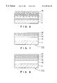
FIG. 7 is a sectional schematic view showing the constitution of a Comparative Example;
FIG. 8 is a sectional schematic view showing the constitution of another Comparative Example; and
FIG. 9 is a view showing the reflectivity spectrum in the visible light region of some of the anti-reflection films of the Examples of the present invention and the Comparative Examples.
BEST MODE FOR CARRYING OUT THE INVENTION
Preferred embodiments of the present invention will now be described with reference to the accompanying drawings.
As shown in FIG. 1 or 2, an anti-reflection film 10 of the present invention has an intermediate refractive index layer (first layer) 3, a high refractive index layer (second layer) 2 and a low refractive index layer (third layer) 1 formed in this sequence on one surface of a transparent base film 5 via a hard coat layer 4 in a mirror shape or given irregularities.
The anti-reflection film 10 is constituted such that
the low refractive index layer 1 comprises an SiOx layer;
the intermediate refractive index layer 3 is constituted on a hard coat layer 4 with irregularities by coating a paint comprising a binder and ultrafine particles having a refractive index of 1.5 or more; and
the high refractive index layer 2 has electric conductivity and electromagnetic shielding properties;
the refractive indices of the adjacent refractive index layers of the respective layers satisfy the relationship: 2.20>refractive index of the high refractive index layer>refractive index of the intermediate refractive index layer (or the intermediate refractive index layer having irregularities)>refractive index of the low refractive index layer>1.40;
the thicknesses of the respective refractive index layers are 80 to 110 nm for the low refractive index layer 1, to 110 nm for the high refractive index layer 2, and 50 to 100 nm for the intermediate refractive index layer 3; and
an optical film thickness D calculated from the equation D=n·d (wherein n=refractive index of the intermediate refractive index layer, and d=thickness of the intermediate refractive index layer) is not larger than the wavelength of visible light.
Preferably, the anti-reflection film 10 is such that the hard coat layer 4 has irregularities on its surface in contact with the intermediate refractive index layer 3, and the hard coat layer 4 is provided on the transparent base film 5 directly or via a primer layer 7 as shown in FIG. 6, or via an adhesive layer 9 as shown in FIG. 5, and the low refractive index layer 1 is provided with an antifouling layer 42.
Preferably, the anti-reflection film 10 is such that the intermediate refractive index layer 3 is composed of 0.1 to 20 parts by weight of a mat material based on one part by weight of a thermosetting resin and/or an ionizing radiation curing resin, the mat material being selected from fine particles of one or more kinds selected from the group consisting of ultrafine particles of ZnO (refractive index 1.90; the values indicated below represent refractive indices), TiO2 (2.3-2.7), CeO2 (1.95), Sb2O5 (1.71), ITO (1.95), Y2O3 (1.87), La2O3 (1.95), ZrO2 (2.05), and Al2O3 (1.95), Zro2 (2.05), and Al2O3 (1.63). The ultrafine particles preferably have a higher refractive index than that of the binder of the intermediate refractive index layer, and have a refractive index of 1.5 or more. The average particle size of the ultrafine particles is preferably 5 to 50 nm, and more preferably 5 to 10 nm.
Preferably, the high refractive index layer 2 and the low refractive index layer 1 are each a layer provided by vacuum coating.
Preferably, the low refractive index layer 1 is formed by plasma CVD involving the discharge of the starting gas of an organosiloxane, and the undecomposed organosiloxane remains in the SiOx layer.
Furthermore, an antifouling layer 42 as shown in FIG. 6 may be formed on the low refractive index layer 1.
The transparent base sheet of the present invention is formed from a ceramic material such as glass, or a transparent stretched or unstretched plastic film.
Besides ordinary optical glass, thermoplastic resins can be used, such as polyester, polyamide, polyimide, polypropylene, polymethylpentene, polyvinyl chloride, polyvinyl acetal, polymethyl methacrylate, polycarbonate, and polyurethane.
On the transparent base film, a hard coat layer having tiny irregularities may be provided directly or through a primer layer for making the adhesion of the hard coat layer firm. On the hard coat layer, an intermediate refractive index layer 3 as shown in FIG. 2 may be provided, and other refractive index layer may be further provided.
The intermediate refractive index layer 3 is lower in refractive index than the high refractive index layer 2, and higher in refractive index than the low refractive index layer 1, hard coat layer 4 and/or transparent base film 5.
The intermediate refractive index layer 3 is preferably provided on the base film 5 by coating a composition comprising a binder and ultrafine particles of a metal oxide as a mat material selected from fine particles of one or more kinds selected from the group consisting of ZnO, TiO2, CeO2 (refractive index 1.95), Sb2O5, SnO2, ITO, Y2O3, La2O3, ZrO2 (refractive index 2.05), Al2O3 and Hf2O3.
The intermediate refractive index layer 3 is formed, as shown in FIG. 3, by coating an uncured hard coat layer 46 on the transparent base film 5, further coating an uncured intermediate refractive index layer 36, laminating these uncured layers to a shaped film 6, heating and/or ionizing radiating treating the laminate to cure the layers, and stripping the shaped film 6 off.
Furthermore, as shown in FIG. 4, the intermediate refractive index layer 3 can be constituted by a transfer method which comprises providing an uncured intermediate refractive index layer 36 and an uncured hard coat layer 46 on a shaped film 6 having irregularities, providing an adhesive layer 9, if desired, on the transparent base film, laminating these layers together, and curing and shaping the laminate.
The ratio of the ultrafme particles to the binder (weight ratio) in the intermediate refractive index layer is preferably 1-20 (ultrafme particles): 1 (binder). If this ratio is less than 1: 1, the effect of anti-reflection decreases. At a ratio of more than 20:1, the adhesion of the ultrafine particles declines, and the ultrafme particles increasingly tend to fall off.
The irregularities for providing the intermediate refractive index layer of the invention may be provided for the shaped hard coat layer 4, but the same function may be imparted by shaping the adhesive layer 9 or primer layer 7, the layer on the transparent base film, into an irregular form. The irregularities of the hard coat layer 4 are in direct contact with the intermediate refractive index layer 3, and the refractive index of the hard coat layer 4 is smaller than the refractive index of the intermediate refractive index layer 3.
The reactive resin that satisfies the foregoing requirements and serves to form the intermediate refractive index layer or the hard coat layer preferably includes, for example, those containing a relatively large amount of a compound having an acrylate type functional group, such as relatively low molecular weight polyester, polyether, acrylic resin, epoxy resin, polyurethane, alkyd resin, spiroacetal resin, polybutadiene, polythiolpolyene resin, an oligomer or prepolymer of (meth)acrylate (in this specification, acrylate and methacrylate are collectively expressed as (meth)acrylate) of a polyfunctional compound such as polyhydric alcohol, and a monofunctional monomer such as ethyl (meth)acrylate, ethylhexyl (meth)acrylate, styrene, vinyltoluene or N-vinylpyrrolidone which is a reactive diluent, and a multifunctional monomer such as trimethylolpropane tri(meth)acrylate, hexanediol (meth)acrylate, tripropylene glycol di(meth)acrylate, diethylene glycol di(meth)acrylate, pentaerythritol tri(meth)acrylate, dipentaerythritol hexa(meth)acrylate, 1,6-hexanediol di(meth)acrylate, or neopentyl glycol di(meth)acrylate.
When the ionizing radiation curing resin is used as an ultraviolet curing resin, it is preferred to incorporate therein a photopolymerization initiator such as acetophenone, benzophenone, Michler's benzoyl benzoate, α-amyloxime ester, or thioxanthone, and a photosensitizer such as n-butylamine, triethylamine, or tri-n-butylphosphine.
The ionizing radiation curing resin may further contain the following reactive organosilicon compound:
A compound of the formula RmSi(OR′)n where R and R′ each denote an alkyl group having 1 to 10 carbon atoms, m+n=4, and m and n each denote an integer. Examples of the compound are tetramethoxysilane, tetraethoxysilane, tetra-iso-propoxysilane, tetra-n-propoxysilane, tetra-n-butoxysilane, tetra-sec-butoxysilane, tetra-tert-butoxysilane, tetrapentaethoxysilane, tetrapenta-iso-propoxysilane, tetrapenta-n-propoxysilane, tetrapenta-n-butoxysilane, tetrapenta-sec-butoxysilane, tetrapenta-tert-butoxysilane, methyltrimethoxysilane, methyltriethoxysilane, methyltripropoxysilane, methyltributoxysilane, dimethyldimethoxysilane, dimethyldiethoxysilane, dimethylethoxysilane, dimethylmethoxysilane, dimethylpropoxysilane, dimethylbutoxysilane, methyldimethoxysilane, methyldiethoxysilane, and hexyltrimethoxysilane.
The thickness of the hard coat layer 4 is preferably 0.5 to 6 μm, more preferably 3 μm or more. If the thickness is less than 0.5 μm, it cannot maintain the hardness of the intermediate refractive index layer, the high refractive index layer and the low refractive index layer formed on the transparent base film. If its thickness is more than 3 μm, satisfactory hardness can be maintained, and hardness performance can be imparted to the anti-reflection film.
Making the hard coat layer thicker than required would impair the flexibility of the anti-reflection film, and take time for curing, imposing restrictions on the productivity and cost.
The term “hardness performance” or “hard coat” as used herein refers to hardness of the grade H or higher according to the pencil hardness test described in JISK5400.
The material for use in the high refractive index layer 2 of the invention should desirably be one higher in refractive index than the binder in the intermediate refractive index layer, and having a refractive index of 1.5 or more. This material may be the same as the fine particle material used in the intermediate refractive index layer.
One or more materials selected from the above-described compounds are used to form the high refractive index layer by vacuum deposition or sputtering. The high refractive index layer is given the highest refractive index of the refractive indices of the respective layers of the invention so that the thickness d of the intermediate refractive index layer will be 80 to 110 nm, and its refractive index will be 1.90 to 2.10. The product of the refractive index n and the thickness d (i.e., the optical thickness D) is adjusted to not larger than the wavelength of visible light so that the reflection of light can be prevented and the transmission of visible light can be optimized.
The high refractive index layer is preferably composed of a sputter film of ITO, and its surface resistance is desirably 103 Ω/□ or less.
In this case, the binder of the intermediate refractive index layer is preferably formed of a thermosetting and/or ionizing radiation curing organosilicon compound. Thus, the adhesion of the intermediate refractive index layer to the above-mentioned ITO layer can be increased further.
The ultrafine particles of the intermediate refractive index layer, particularly preferably, comprise ZrO2 particles to impart better durability.
The low refractive index layer of the invention comprises SiOx (x=1.5-4.0), and can be formed by CVD, or preferably by plasma CVD using an organosiloxane as the starting gas under conditions under which no other inorganic vacuum deposition source exists. The vacuum deposited film is maintained at as low a temperature as possible.
The SiOx layer (low refractive index layer) of the invention is adapted to contain the undecomposed organosiloxane and to have carbon remaining at a ratio of 0.1-0.2 to silicon. Thus, the effect of maintaining the flexibility and adhesion of SiOx can be enhanced further.
The thus formed low refractive index layer comprises the SiOx layer with a contact angle of the surface to water of from 40 to 180 degrees. Hence, this layer is also effective in preventing the deposition of dust.
A polarizing plate having the so constituted anti-reflection film 10 laminated on a polarizer, or a cathode-ray tube with the anti-reflection film 10 bonded onto the surface gives a sharp image and is reflection-free.
A liquid crystal display device with the polarizing plate built-in shows a sharp image free from reflected light.
The present invention will now be described in more detail by reference to Examples.
EXAMPLE 1
On one surface of a 50 μm thick biaxially stretched polyethylene terephthalate film (Lumirror T-60#50, TORAY INDUSTRIES, INC.) as a shaped film 6 as shown in FIG. 4, ZrO2 fine particle coating solution No. 1275 [a coating solution comprising 0.3 part by weight of a binder (an ionizing radiation curing organosilicon compound) per 100 parts by weight of ZrO2 fine particles; Sumitomo Osaka Cement Co., Ltd.] was coated to a thickness of 57 nm (dry thickness; the same holds in the following description) by means of a wire bar to form an uncured intermediate refractive index layer 36 (refractive index 1.74).
Separately, an ultraviolet curing resin (PET-D31, DAINICHISEIKA COLOUR & CHEMICALS MFG. CO., LTD.) was coated on a 188 μm thick PET film (A-4350#188, TOYOBO, CO., LTD.) as a transparent base film 5 to a thickness of 6 μm, followed by drying the solvent component, to form an uncured hard coat layer 46.
Then, the uncured intermediate refractive index layer 36 provided on the shaped film 6, and the uncured hard coat layer 46 provided on the transparent base film 5 were laminated and pressure-bonded together in contact with each other. Then, the laminate was irradiated with ultraviolet rays at a dose of 480 mJ (10 m/min) to cure the uncured intermediate refractive index layer 36 and hard coat layer 46 to form an intermediate refractive index layer 3 and a hard coat layer 4. Then, the shaped film 6 was peeled off.
As shown in FIG. 4B, the transparent base film 5 cleared of the peeled shaped film 6H had the hard coat layer 4 and the intermediate refractive index layer 3 superimposed thereon with the fine particles of the intermediate refractive index layer 3 embedded in and transferred to the surface of the hard coat layer 4.
Further, as shown in FIG. 4C, ITO sputtering (refractive index 2.0) was performed on the side of the intermediate refractive index layer 3 under the conditions, a vacuum of 5×10⁻⁶ torr, a base plate temperature of room temperature, argon of 100 scc/min, oxygen of 5 scc/min, and a deposit rate of 1.6 Å/s, to form a high refractive index layer 2 with a thickness of 105 nm.
On the high refractive index layer 2, SiO2 (refractive index 1.46) was vacuum deposited under the conditions, a vacuum of 5×10⁻⁶ torr, a base plate temperature of room temperature, and a deposit rate of 26 Å/s, to form a low refractive index layer 1 with a thickness of 85 nm.
On the low refractive index layer 1 side, fluorine surfactant FC-772 (a product of 3M) was further coated to a thickness of 2 nm by means of a wire bar to complete an anti-reflection film 10 of Example 1.
EXAMPLE 2
On one surface of MC-19 (a product of Reiko Co., Ltd.) as a 50 μm thick shaped film 6 surface treated with acrylic melamine resin, as shown in FIG. 5, ZrO2 fine particle coating solution No. 1221 [a coating solution comprising 0.3 part by weight of a binder (an ionizing radiation curing organosilicon compound) per 100 parts by weight of Zro2 fine particles; Sumitomo Osaka Cement Co., Ltd.] was coated to a thickness of 57 nm by means of a wire bar to form an uncured intermediate refractive index layer 36 (refractive index 1.74).
On the intermediate refractive index layer 36 side, an ultraviolet curing resin (PET-D31, DAINICHISEIKA COLOUR & CHEMICALS MFG. CO., LTD.) was coated to a thickness of 8 μm, followed by drying the solvent component, to form an uncured hard coat layer 46.
Then, the uncured intermediate refractive index layer 36 and the uncured hard coat layer 46 were irradiated with ultraviolet rays at a dose of 480 mJ (10 m/min) to cure the uncured intermediate refractive index layer and hard coat layer to provide an intermediate refractive index layer 3 and a hard coat layer 4 on the shaped film 6.
As a result, the fine particles of the intermediate refractive index layer 3 were embedded in and transferred to the surface of the transparent cured resin layer 4, and the hard coat layer 4 and the intermediate refractive index layer 3 were superimposed on the transparent shaped film 6.
On the hard coat layer 4 side, a urethane-derived two-component setting adhesive LX-660/KW75=4/1 (a product of DIC) was coated to a thickness of 10 μm by wire bar coating to form an uncured adhesive layer 43. On the layer 43, a triacetyl cellulose film FT-UV80 (a product of Fuji Photo Film Co., Ltd.) was superimposed as a transparent base film 5. The laminate was aged for 7 days at 40° C. to complete the curing of the adhesive, forming a transparent cured adhesive layer 9, followed by stripping off the shaped film 6H. On the surface of the intermediate refractive index layer 3 deprived of the peeled shaped film 6H, ITO sputtering was performed under the same conditions as in Example 1 to form a high refractive index layer 2. SiO2 was further superimposed on the high refractive index layer 2 by plasma CVD to complete an anti-reflection film 10 of Example 2.
EXAMPLE 3
On one surface of a 188 μm thick biaxially stretched polyethylene terephthalate film T-PET (A-4350, TOYOBO CO., LTD.) as a transparent base film 5 as shown in FIG. 3, the same uncured hard coat layer 46 as used in Example 1 was applied to a thickness of 8 μm. Also, a coating solution comprising 0.4 part by weight of a binder per 100 parts by weight of TiO2 fine particles (the coating solution produced by Sumitomo Osaka Cement Co., Ltd.] was coated to a thickness of 57 nm by means of a wire bar to form an uncured intermediate refractive index layer 36 (refractive index 1.74).
On the surface of the uncured intermediate refractive index layer 36, the same shaped film 6 as used in Example 1 was superimposed, following by curing the laminate.
Thus, a hard coat layer 4 and an intermediate refractive index layer 3 having irregularities were formed in the same manner as in Example 1, followed by stripping off a strippable shaped film 6H.
On the side of the intermediate refractive index layer 3, a 105 nm thick, high refractive index layer 2 by ITO sputtering (refractive index 2.0), and a 85 nm thick, low refractive index layer 1 of SiO2 (refractive index 1.46) were formed.
On the low refractive index layer 1 side, the same fluorine surfactant FC-772 as used in Example 1 was further coated to a thickness of 2 nm to complete an anti-reflection film 10 of Example 3 that used TiO2 instead of ZrO2 in Example 1.
Comparative Example 1
As shown in FIG. 7, a hard coat layer 45 with a thickness of 8 μm was provided on a 188 μm thick PET film (A-4350#188, TOYOBO, CO., LTD.) as a transparent base film 5. Further, MgO (refractive index 1.72) was vacuum deposited to a thickness of 57 nm to provide a refracting layer 26. Then, a refracting layer 27 by ITO sputtering and a refracting layer 28 by vacuum deposition of SiO2 were provided in the same manner as in Example 1 to complete an anti-reflection film 10H of a Comparative Example.
Comparative Example 2
An anti-reflection film of Comparative Example 2 was prepared in the same manner as in Comparative Example 1, except that the second refracting layer was formed by vacuum deposition of TiO2 instead of ITO sputtering.
A hard coat layer 45 with a thickness of 8 μm was provided on one surface of a base film 5. Further, MgO (refractive index 1.72) was vacuum deposited to a thickness of 57 nm to provide a refracting layer 26. Then, a highly refracting layer 27 (film thickness 100 nm) by vacuum deposition of TiO2, and a refracting layer 28 (film thickness 85 nm) by vacuum deposition of SiO2 were provided to complete an anti-reflection film 10H of a Comparative Example.
Comparative Example 3
As shown in FIG. 8, a hard coat layer 45 with a thickness of 8 μm was provided on a transparent base film 5 in the same manner as in Comparative Example 1.
Further, ITO sputtering (refractive index 2.0) was performed on the side of the hard coat layer 45 under the conditions, a vacuum of 5×10⁻⁶ torr, a base plate temperature of room temperature, argon of 100 scc/min, oxygen of 5 scc/min, and a deposit rate of 1.6 Å/s, to form a first refractive index layer 26 with a thickness of 25 nm.
On the first refractive index layer 26, SiO2 (refractive index 1.43) was vacuum deposited under the conditions, a vacuum of 5×10⁻⁶ torr, a base plate temperature of room temperature, and a deposit rate of 2 Å/s, to form a second refractive index layer 27 with a thickness of 20 nm.
Further, ITO sputtering was performed on the side of the second refractive index layer 27 under the conditions, a vacuum of 5×10⁻⁶ torr, a base plate temperature of room temperature, argon of 100 scc/min, oxygen of 5 scc/min, and a deposit rate of 1.6 Å/s, to form a third refractive index layer 28 with a thickness of 120 nm.
On the third refractive index layer 28, vacuum deposition of SiO2 was performed under the conditions, a vacuum of 5×10⁻⁶ torr, a base plate temperature of room temperature, and a deposit rate of 2 Å/s, to form a fourth refractive index layer 29 with a thickness of 100 nm, thereby completing an anti-reflection film of Comparative Example 3.
EXAMPLE 4
An anti-reflection film was prepared in the same manner as in Example 1, except that
the film thickness of the intermediate refractive index layer (ZrO2:n=1.74)=90 nm,
the film thickness of the high refractive index layer (ITO:n=2.0)=40 nm, and
the film thickness of the low refractive index layer (SiO2:n=1.46)=100 nm.
Comparative Example 4
Although not shown, a 7 μm thick hard coat layer 45 as used in Comparative Example 4 was provided on a PET film 5 in the same manner as in Comparative Example 4. Further, ITO and SiO2 were vacuum deposited in this order to optical film thicknesses of (λ/4-λ/4), i.e., deposited laminated film thicknesses 69 nm and 94 nm, respectively, as two refracting layers consisting of a first refracting layer and a second refracting layer. Thus, an anti-reflection film of Comparative Example 4 was prepared.
The samples obtained in the Examples and Comparative Examples were measured for the spectral drawings of anti-reflection films to investigate the low reflectivity region less than 1%. The samples were also measured for surface characteristics (surface resistance, measured by the four-terminal method; contact angle of surface, measured by Model G1, a contact angle measuring instrument of Elmer; humidity resistance test, a test for visual evaluation of a change in appearance after the sample is allowed to stand for 48 hours in an environment of 50° C. and relative humidity of 95%; and coefficient of dynamic friction).
The results of measurement are shown in FIG. 9 and Table 1.
TABLE 1
Low
Evaluation reflectivity Surface Contact angle Coefficient of Humidity
item region registance of surface dynamic resistance Carbon:
Sample nm Ω/□ Degrees friction test silicon
Ex. 1 415-705 63 113 0.80 No change 0
Ex. 2 420-720 65 112 0.80 No change   0.1
Ex. 3 420-720 64 114 0.79 No change 0
Ex. 4 435-700 122  112 0.80 No change 0
Comp. Ex. 1 430-700 63  33 1.23 Separated* 0
Comp. Ex. 2 390-700 1015  31 1.32 Separated* 0
Comp. Ex. 3 450-710 66  30 1.23 No change 0
Comp. Ex. 4 525-580 64  34 1.33 No change 0
*Separated: The optical thin layer formed by vacuum coating separated from the surface of the intermediate refractive index layer.
The anti-reflection film 10 of the present invention comprises a hard coat layer, an intermediate refractive index layer, a high refractive index layer and a low refractive index layer formed in this sequence on a base film. The hard coat layer is formed from a thermosetting or ionizing radiation curing resin. Thus, an anti-reflection film with firm, stable adhesion of the layers to the base film and having excellent anti-glare properties can be provided.
Furthermore, the refracting layers of the anti-reflection films of Examples 1 and 2 are composed of three layers. Nevertheless, these anti-reflection films give an anti-reflection effect comparable to that of the four-layer product of Comparative Example 2, and they are advantageous in that the number of steps can be decreased compared with the four-layer product.

Claims (9)

What is claimed is:
1. An anti-reflection film having an intermediate refractive index layer, a high refractive index layer and a low refractive index layer formed in this order on a transparent base film through a hard coat layer, said anti-reflection film comprising:
the low refractive index layer comprising an SiOx layer where x is 1.5 to 4.0;
the intermediate refractive index layer comprising a coating of a composition comprising a binder and ultrafine particles having a refractive index of 1.5 or more; and
the high refractive index layer; and
said anti-reflection film having:
the relationship 2.20>refractive index of the high refractive index layer>refractive index of the intermediate refractive index layer>refractive index of the low refractive index layer>1.40;
the thickness of each refractive index layer being 80 to 110 nm for the low refractive index layer, 30 to 110 nm for the high refractive index layer, and 50 to 100 nm for the intermediate refractive index layer; and
an optical film thickness D not larger than the wavelength of visible light (D=n·d wherein n is the refractive index of the intermediate refractive index layer and d is the thickness of the intermediate refractive index layer).
2. An anti-reflection film as claimed in claim 1, wherein the hard coat layer has irregularities on its surface in contact with the intermediate refractive index layer.
3. An anti-reflection film as claimed in claim 1, wherein the hard coat layer is provided on the transparent base film directly or through a primer layer and/or an adhesive layer.
4. An anti-reflection film as claimed in claim 1, wherein the intermediate refractive index layer comprises 1 part by weight of a thermosetting resin and/or an ionizing radiation curing resin and 0.1 to 20 parts by weight of ultrafine particles of one or more kinds selected from the group consisting of ultra-fine particles of ZnO, TiO2, CeO2, Sb2O5, SnO2, ITO, Y2O3, La2O3, Al2O3, Hf2O3 and ZrO2.
5. An anti-reflection film as claimed in claim 1, wherein the high refractive index layer and the low refractive index layer are each a layer provided by vacuum coating.
6. An anti-reflection film as claimed in claim 1, wherein the low refractive index layer is formed by plasma CVD involving the discharge of the starting gas of an organosiloxane, and the undecomposed organosiloxane remains in an amount of 0.1 to 0.2 parts of carbon based on one part of silicon.
7. An anti-reflection film as claimed in claim 1, wherein an antifouling layer may be formed on the low refractive index layer.
8. An anti-reflection film having an intermediate refractive index layer, a high refractive index layer and a low refractive index layer formed in this order on a transparent base film through a hard coat layer, said anti-reflection film comprising:
the low refractive index layer comprising an SiOx layer where x is 1.5 to 4.0;
the intermediate refractive index layer constituted by coating a paint comprising a binder and ultrafine particles having a refractive index of 1.5 or more; and
the high refractive index layer having electric conductivity; and
said anti-reflection film having:
the relationship 2.20>refractive index of the high refractive index layer>refractive index of the intermediate refractive index layer>refractive index of the low refractive index layer>1.40; and
the ultrafine particles of the intermediate refractive index layer comprising ZrO2 particles.
9. An anti-reflection film as claimed in claim 1, wherein the high refractive index layer has electric conductivity.
US09/007,796 1997-01-20 1998-01-15 Anti-reflection film and process for preparation thereof Expired - Lifetime US6207263B1 (en)

Priority Applications (1)

Application Number Priority Date Filing Date Title
US09/754,130 US20010021446A1 (en) 1997-01-20 2001-01-05 Anti-reflection film and process for preparation thereof

Applications Claiming Priority (2)

Application Number Priority Date Filing Date Title
JP9-019562 1997-01-20
JP9019562A JPH10206603A (en) 1997-01-20 1997-01-20 Reflection preventive film and manufacture thereof

Related Child Applications (1)

Application Number Title Priority Date Filing Date
US09/754,130 Division US20010021446A1 (en) 1997-01-20 2001-01-05 Anti-reflection film and process for preparation thereof

Publications (1)

Publication Number Publication Date
US6207263B1 true US6207263B1 (en) 2001-03-27

Family

ID=12002750

Family Applications (2)

Application Number Title Priority Date Filing Date
US09/007,796 Expired - Lifetime US6207263B1 (en) 1997-01-20 1998-01-15 Anti-reflection film and process for preparation thereof
US09/754,130 Abandoned US20010021446A1 (en) 1997-01-20 2001-01-05 Anti-reflection film and process for preparation thereof

Family Applications After (1)

Application Number Title Priority Date Filing Date
US09/754,130 Abandoned US20010021446A1 (en) 1997-01-20 2001-01-05 Anti-reflection film and process for preparation thereof

Country Status (2)

Country Link
US (2) US6207263B1 (en)
JP (1) JPH10206603A (en)

Cited By (47)

* Cited by examiner, † Cited by third party
Publication number Priority date Publication date Assignee Title
US20030049866A1 (en) * 2001-09-05 2003-03-13 Genicon Sciences Corporation Sample device preservation
US20030096302A1 (en) * 2001-02-23 2003-05-22 Genicon Sciences Corporation Methods for providing extended dynamic range in analyte assays
US6592950B1 (en) * 1998-02-12 2003-07-15 Kimoto Co., Ltd. Anti-Newton ring film
EP1367653A1 (en) 2002-05-27 2003-12-03 Centro De Investigaciones Energeticas Medioambientales Y Tecnologicas (C.I.E.M.A.T.) Method for preparing transparent and conducting sheets on polymers
US6689479B2 (en) * 2001-08-28 2004-02-10 Dai Nippon Printing Co., Ltd. Anti-reflection film, and silica layer
US20040070727A1 (en) * 2002-10-11 2004-04-15 Nicoh Optical Co., Ltd. Metallic vapor deposition lens provided with a protection coat and a method of producing the same
US6753064B1 (en) * 1997-10-24 2004-06-22 Nippon Sheet Glass Co., Ltd. Multi-layered coated substrate and method of production thereof
US20040209056A1 (en) * 2001-07-05 2004-10-21 Isamu Oguri Antireflection film and method for production thereof
US20050112784A1 (en) * 1996-04-25 2005-05-26 Genicon Sciences Corporation Analyte assay using particulate labels
US20050136180A1 (en) * 2003-12-19 2005-06-23 3M Innovative Properties Company Method of coating a substrate with a fluoropolymer
US20050141843A1 (en) * 2003-12-31 2005-06-30 Invitrogen Corporation Waveguide comprising scattered light detectable particles
US20050192408A1 (en) * 2001-10-04 2005-09-01 Bridggestone Corporation Nano-particle preparation and applications
US20050228074A1 (en) * 2004-04-05 2005-10-13 Bridgestone Corporation Amphiphilic polymer micelles and use thereof
US20060008618A1 (en) * 2004-07-06 2006-01-12 Xiaorong Wang Hydrophobic surfaces with nanoparticles
US20060134426A1 (en) * 2004-09-29 2006-06-22 Dai Nippon Printing Co., Ltd. Optical laminate
US20060134429A1 (en) * 2004-09-29 2006-06-22 Dai Nippon Printing Co., Ltd. Optical laminate
US20060154094A1 (en) * 2002-12-02 2006-07-13 Mitsubishi Polyester Film Corporation Biaxially oriented laminated polyester film
US20060164740A1 (en) * 2003-06-26 2006-07-27 Atsushi Sone Optical multilayer film, polarizing plate and optical product
US20060210767A1 (en) * 2003-03-31 2006-09-21 Yasumasa Yoshitomi Polarization plate protection film
US20070092730A1 (en) * 2005-10-24 2007-04-26 Hitachi Maxell, Ltd. Optical film and method for producing the same
US20070142550A1 (en) * 2005-12-16 2007-06-21 Bridgestone Corporation Combined use of liquid polymer and polymeric nanoparticles for rubber applications
US20070149649A1 (en) * 2005-12-19 2007-06-28 Xiaorong Wang Non-spherical nanoparticles made from living triblock polymer chains
US20070185273A1 (en) * 2004-01-12 2007-08-09 Xiaorong Wang Polymeric Nano-Particles Of Flower-Like Structure And Applications
US20070196653A1 (en) * 2005-12-20 2007-08-23 Hall James E Vulcanizable nanoparticles having a core with a high glass transition temperature
US20070231479A1 (en) * 2006-03-30 2007-10-04 Fujifilm Corporation Coating apparatus, coating method, and method for manufacturing optical film
US20070275218A1 (en) * 2006-05-10 2007-11-29 Fujifilm Corporation Multilayer film and image display device
US20080027972A1 (en) * 2006-07-31 2008-01-31 Sap Portals Israel Ltd. Method for application modeling
CN100388013C (en) * 2005-01-14 2008-05-14 索尼株式会社 Optical device, transmission lens, image pickup device and electronic device
US20080286374A1 (en) * 2005-12-20 2008-11-20 Xiaorong Wang Hollow nano-particles and method thereof
US20080305336A1 (en) * 2004-06-21 2008-12-11 Xiaorong Wang Reversible Polymer/Metal Nano-Composites And Method For Manufacturing Same
US20090005491A1 (en) * 2007-06-29 2009-01-01 Sandra Warren One-Pot Synthesis Of Nanoparticles And Liquid Polymer For Rubber Applications
US20090052041A1 (en) * 2007-08-20 2009-02-26 Toppan Printing, Co., Ltd. Anti-Reflection Film and Polarizing Plate Using the Same
US20090054554A1 (en) * 2005-12-19 2009-02-26 Xiaorong Wang Disk-like Nanoparticles
US20100016472A1 (en) * 2004-03-02 2010-01-21 Xiaorong Wang Rubber Composition Containing Functionalized Polymer Nanoparticles
US20100016512A1 (en) * 2006-12-19 2010-01-21 Xiaorong Wang Fluorescent Nanoparticles
CN1955762B (en) * 2005-10-24 2010-06-09 日立麦克赛尔株式会社 Optical film and method for manufacturing the same
US20100297365A1 (en) * 2009-05-22 2010-11-25 Curd Alistair P Optical structure to reduce internal reflections
US20110172364A1 (en) * 2009-12-29 2011-07-14 Chen Yaohong Charged Nanoparticles And Method Of Controlling Charge
US20110213066A1 (en) * 2009-04-03 2011-09-01 Xiaorong Wang Hairy Polymeric Nanoparticles With First And Second Shell Block Polymer Arms
US20110236686A1 (en) * 2009-12-29 2011-09-29 Hideki Kitano Well Defined, Highly Crosslinked Nanoparticles And Method For Making Same
US8541503B2 (en) 2006-07-28 2013-09-24 Bridgestone Corporation Polymeric core-shell nanoparticles with interphase region
US8846819B2 (en) 2008-12-31 2014-09-30 Bridgestone Corporation Core-first nanoparticle formation process, nanoparticle, and composition
US9428604B1 (en) 2011-12-30 2016-08-30 Bridgestone Corporation Nanoparticle fillers and methods of mixing into elastomers
US9851473B2 (en) 2013-01-29 2017-12-26 Nitto Denko Corporation Anti-reflection film and production method therefor
US11709156B2 (en) 2017-09-18 2023-07-25 Waters Technologies Corporation Use of vapor deposition coated flow paths for improved analytical analysis
US11709155B2 (en) 2017-09-18 2023-07-25 Waters Technologies Corporation Use of vapor deposition coated flow paths for improved chromatography of metal interacting analytes
US11918936B2 (en) 2020-01-17 2024-03-05 Waters Technologies Corporation Performance and dynamic range for oligonucleotide bioanalysis through reduction of non specific binding

Families Citing this family (27)

* Cited by examiner, † Cited by third party
Publication number Priority date Publication date Assignee Title
JP3541606B2 (en) * 1997-03-05 2004-07-14 住友化学工業株式会社 Low reflection resin substrate
TW415888B (en) * 1998-02-17 2000-12-21 Nippon Kayaku Kk Transparent sheet or film
JPH11258405A (en) * 1998-03-12 1999-09-24 Toppan Printing Co Ltd Antireflection film
JP3975036B2 (en) * 1998-09-22 2007-09-12 富士フイルム株式会社 Method for manufacturing antireflection film
JP4097102B2 (en) * 1998-09-25 2008-06-11 大日本印刷株式会社 Antistatic coloring hard coat film and display device
JP2000121804A (en) * 1998-10-09 2000-04-28 Sekisui Chem Co Ltd Antireflection film
GB2345021A (en) * 1998-12-22 2000-06-28 Nokia Mobile Phones Ltd Matt surface display window
TWI246460B (en) * 1999-01-14 2006-01-01 Sumitomo Chemical Co Anti-reflection film
JP2001021701A (en) * 1999-07-09 2001-01-26 Sumitomo Osaka Cement Co Ltd Transparent film with electrification and reflection prevention film
JP5004065B2 (en) * 2000-05-19 2012-08-22 東レフィルム加工株式会社 Laminated film and method for producing the same
JP2002103507A (en) * 2000-09-29 2002-04-09 Dainippon Printing Co Ltd Silica layer and reflection preventing film using the same
JP3751922B2 (en) * 2001-08-28 2006-03-08 大日本印刷株式会社 Antireflection film, and display device and liquid crystal display device using the same
JP2003090902A (en) * 2001-09-19 2003-03-28 Dainippon Printing Co Ltd Antireflection imparting film and antireflection processing method using the same
JP2004009420A (en) * 2002-06-05 2004-01-15 Nakajima Kogyo Kk Low reflective transferring foil, process of manufacturing molding, and molding
JP4187477B2 (en) * 2002-08-05 2008-11-26 大日本印刷株式会社 Low reflection film
JP2004309898A (en) * 2003-04-09 2004-11-04 Teijin Dupont Films Japan Ltd Antireflection film
JP2007182024A (en) * 2006-01-10 2007-07-19 Kitagawa Ind Co Ltd Anti-glare film
JP5199162B2 (en) * 2009-03-27 2013-05-15 富士フイルム株式会社 Functional film manufacturing method and manufacturing apparatus
CN102463714B (en) * 2010-11-11 2015-04-15 鸿富锦精密工业(深圳)有限公司 Covered element with fingerprint resistance and manufacture method thereof
US9435626B2 (en) * 2011-08-12 2016-09-06 Corning Incorporated Kinematic fixture for transparent part metrology
JP5644753B2 (en) * 2011-12-26 2014-12-24 豊田合成株式会社 Group III nitride semiconductor light emitting device
JP2013156523A (en) * 2012-01-31 2013-08-15 Topcon Corp Substrate
CN105593713B (en) 2013-10-03 2018-07-31 富士胶片株式会社 Projected image is shown with half-reflecting mirror and its manufacturing method and projection image display system
JP6730803B2 (en) * 2015-12-18 2020-07-29 デクセリアルズ株式会社 Method for forming antireflection optical body, display panel and optical film
CN106959479B (en) * 2016-04-01 2019-05-24 江苏集萃智能液晶科技有限公司 A kind of optical film
CN110799330B (en) * 2017-07-03 2022-12-27 迪睿合电子材料有限公司 Fine uneven laminate, method for producing same, and camera module mounting device
KR102032316B1 (en) * 2018-07-09 2019-10-15 에스케이씨 주식회사 Optical multilayer film, optical component and display device comprising same

Cited By (92)

* Cited by examiner, † Cited by third party
Publication number Priority date Publication date Assignee Title
US20050112784A1 (en) * 1996-04-25 2005-05-26 Genicon Sciences Corporation Analyte assay using particulate labels
US6753064B1 (en) * 1997-10-24 2004-06-22 Nippon Sheet Glass Co., Ltd. Multi-layered coated substrate and method of production thereof
US6592950B1 (en) * 1998-02-12 2003-07-15 Kimoto Co., Ltd. Anti-Newton ring film
US20030096302A1 (en) * 2001-02-23 2003-05-22 Genicon Sciences Corporation Methods for providing extended dynamic range in analyte assays
US7361472B2 (en) 2001-02-23 2008-04-22 Invitrogen Corporation Methods for providing extended dynamic range in analyte assays
US20090015831A1 (en) * 2001-02-23 2009-01-15 Juan Yguerabide Methods for providing extended dynamic range in analyte assays
US20070148352A1 (en) * 2001-07-05 2007-06-28 Teijin Dupont Films Japan Limited Antireflective film and production method thereof
US20040209056A1 (en) * 2001-07-05 2004-10-21 Isamu Oguri Antireflection film and method for production thereof
US6689479B2 (en) * 2001-08-28 2004-02-10 Dai Nippon Printing Co., Ltd. Anti-reflection film, and silica layer
US20100069259A1 (en) * 2001-09-05 2010-03-18 Invitrogen Corporation Sample device preservation
US20030049866A1 (en) * 2001-09-05 2003-03-13 Genicon Sciences Corporation Sample device preservation
US20030124733A1 (en) * 2001-09-05 2003-07-03 Genicon Sciences Corporation Sample device preservation
US20100081579A1 (en) * 2001-09-05 2010-04-01 Invitrogen Corporation Sample device preservation
US8057899B2 (en) 2001-10-04 2011-11-15 Bridgestone Corporation Nano-particle preparation and applications
US20050192408A1 (en) * 2001-10-04 2005-09-01 Bridggestone Corporation Nano-particle preparation and applications
US7795344B2 (en) 2001-10-04 2010-09-14 Bridgestone Corporation Nano-particle preparation and applications
US20060084722A1 (en) * 2001-10-04 2006-04-20 Bohm Georg G A Self assembly of molecules to form nano-particles
US20090048390A1 (en) * 2001-10-04 2009-02-19 Xiaorong Wang Nano-Particle Preparation And Applications
US7718738B2 (en) 2001-10-04 2010-05-18 Bridgestone Corporation Self assembly of molecules to form nano-particles
EP1367653A1 (en) 2002-05-27 2003-12-03 Centro De Investigaciones Energeticas Medioambientales Y Tecnologicas (C.I.E.M.A.T.) Method for preparing transparent and conducting sheets on polymers
US20040070727A1 (en) * 2002-10-11 2004-04-15 Nicoh Optical Co., Ltd. Metallic vapor deposition lens provided with a protection coat and a method of producing the same
US20040229056A1 (en) * 2002-10-11 2004-11-18 Nicoh Optical Co., Ltd. Metallic vapor deposition lens provided with a protection coat and a method of producing the same
US6817712B2 (en) * 2002-10-11 2004-11-16 Nicoh Optical Co., Ltd. Metallic vapor deposition lens provided with a protection coat and a method of producing the same
US20060154094A1 (en) * 2002-12-02 2006-07-13 Mitsubishi Polyester Film Corporation Biaxially oriented laminated polyester film
US7223467B2 (en) * 2002-12-02 2007-05-29 Mitsubishi Polyester Film Corporation Biaxially oriented laminated polyester film
US20060210767A1 (en) * 2003-03-31 2006-09-21 Yasumasa Yoshitomi Polarization plate protection film
US7413810B2 (en) * 2003-03-31 2008-08-19 Zeon Corporation Polarization plate protection film
US7285323B2 (en) * 2003-06-26 2007-10-23 Zeon Corporation Optical multilayer film, polarizing plate and optical product
US20060164740A1 (en) * 2003-06-26 2006-07-27 Atsushi Sone Optical multilayer film, polarizing plate and optical product
US20050136180A1 (en) * 2003-12-19 2005-06-23 3M Innovative Properties Company Method of coating a substrate with a fluoropolymer
US20050141843A1 (en) * 2003-12-31 2005-06-30 Invitrogen Corporation Waveguide comprising scattered light detectable particles
US20070185273A1 (en) * 2004-01-12 2007-08-09 Xiaorong Wang Polymeric Nano-Particles Of Flower-Like Structure And Applications
US7786236B2 (en) 2004-01-12 2010-08-31 Bridgestone Corporation Polymeric nano-particles of flower-like structure and applications
US7718737B2 (en) 2004-03-02 2010-05-18 Bridgestone Corporation Rubber composition containing functionalized polymer nanoparticles
US20100016472A1 (en) * 2004-03-02 2010-01-21 Xiaorong Wang Rubber Composition Containing Functionalized Polymer Nanoparticles
US7897690B2 (en) 2004-03-02 2011-03-01 Bridgestone Corporation Rubber composition containing functionalized polymer nanoparticles
US20050228074A1 (en) * 2004-04-05 2005-10-13 Bridgestone Corporation Amphiphilic polymer micelles and use thereof
US20080160305A1 (en) * 2004-04-05 2008-07-03 Bridgestone Corporation Amphiphilic polymer micelles and use thereof
US8349964B2 (en) 2004-06-21 2013-01-08 Bridgestone Corporation Reversible polymer/metal nano-composites and method for manufacturing same
US20080305336A1 (en) * 2004-06-21 2008-12-11 Xiaorong Wang Reversible Polymer/Metal Nano-Composites And Method For Manufacturing Same
US20060008618A1 (en) * 2004-07-06 2006-01-12 Xiaorong Wang Hydrophobic surfaces with nanoparticles
US7998554B2 (en) * 2004-07-06 2011-08-16 Bridgestone Corporation Hydrophobic surfaces with nanoparticles
US7534491B2 (en) * 2004-09-29 2009-05-19 Dai Nippon Printing Co., Ltd. Optical laminate
US7662483B2 (en) * 2004-09-29 2010-02-16 Dai Nippon Printing Co., Ltd. Optical laminate
US20060134426A1 (en) * 2004-09-29 2006-06-22 Dai Nippon Printing Co., Ltd. Optical laminate
TWI391250B (en) * 2004-09-29 2013-04-01 Dainippon Printing Co Ltd Optical laminate
US20060134429A1 (en) * 2004-09-29 2006-06-22 Dai Nippon Printing Co., Ltd. Optical laminate
CN100388013C (en) * 2005-01-14 2008-05-14 索尼株式会社 Optical device, transmission lens, image pickup device and electronic device
CN1955762B (en) * 2005-10-24 2010-06-09 日立麦克赛尔株式会社 Optical film and method for manufacturing the same
US7871717B2 (en) * 2005-10-24 2011-01-18 Hitachi Maxell, Ltd. Optical film and method for producing the same
US20070092730A1 (en) * 2005-10-24 2007-04-26 Hitachi Maxell, Ltd. Optical film and method for producing the same
US9061900B2 (en) 2005-12-16 2015-06-23 Bridgestone Corporation Combined use of liquid polymer and polymeric nanoparticles for rubber applications
US20070142550A1 (en) * 2005-12-16 2007-06-21 Bridgestone Corporation Combined use of liquid polymer and polymeric nanoparticles for rubber applications
US20070149649A1 (en) * 2005-12-19 2007-06-28 Xiaorong Wang Non-spherical nanoparticles made from living triblock polymer chains
US8288473B2 (en) 2005-12-19 2012-10-16 Bridgestone Corporation Disk-like nanoparticles
US8957154B2 (en) 2005-12-19 2015-02-17 Bridgestone Corporation Disk-like nanoparticles
US20090054554A1 (en) * 2005-12-19 2009-02-26 Xiaorong Wang Disk-like Nanoparticles
US7884160B2 (en) 2005-12-19 2011-02-08 Bridgestone Corporation Non-spherical nanoparticles made from living triblock polymer chains
US20070196653A1 (en) * 2005-12-20 2007-08-23 Hall James E Vulcanizable nanoparticles having a core with a high glass transition temperature
US20080286374A1 (en) * 2005-12-20 2008-11-20 Xiaorong Wang Hollow nano-particles and method thereof
US8697775B2 (en) 2005-12-20 2014-04-15 Bridgestone Corporation Vulcanizable nanoparticles having a core with a high glass transition temperature
US10023713B2 (en) 2005-12-20 2018-07-17 Bridgestone Corporation Hollow nano-particles and method thereof
US8877250B2 (en) 2005-12-20 2014-11-04 Bridgestone Corporation Hollow nano-particles and method thereof
US7713579B2 (en) 2006-03-30 2010-05-11 Fujifilm Corporation Coating apparatus, coating method, and method for manufacturing optical film
US20070231479A1 (en) * 2006-03-30 2007-10-04 Fujifilm Corporation Coating apparatus, coating method, and method for manufacturing optical film
US20070275218A1 (en) * 2006-05-10 2007-11-29 Fujifilm Corporation Multilayer film and image display device
US7541087B2 (en) * 2006-05-10 2009-06-02 Fujifilm Corporation Multilayer film and image display device
US8541503B2 (en) 2006-07-28 2013-09-24 Bridgestone Corporation Polymeric core-shell nanoparticles with interphase region
US20080027972A1 (en) * 2006-07-31 2008-01-31 Sap Portals Israel Ltd. Method for application modeling
US8410225B2 (en) 2006-12-19 2013-04-02 Bridgestone Corporation Fluorescent nanoparticles
US20100016512A1 (en) * 2006-12-19 2010-01-21 Xiaorong Wang Fluorescent Nanoparticles
US20100324167A1 (en) * 2007-06-29 2010-12-23 Sandra Warren One-pot synthesis of nanoparticles and liquid polymer for rubber applications
US7829624B2 (en) 2007-06-29 2010-11-09 Bridgestone Corporation One-pot synthesis of nanoparticles and liquid polymer for rubber applications
US20090005491A1 (en) * 2007-06-29 2009-01-01 Sandra Warren One-Pot Synthesis Of Nanoparticles And Liquid Polymer For Rubber Applications
US20090052041A1 (en) * 2007-08-20 2009-02-26 Toppan Printing, Co., Ltd. Anti-Reflection Film and Polarizing Plate Using the Same
US9631056B2 (en) 2008-12-31 2017-04-25 Bridgestone Corporation Core-first nanoparticle formation process, nanoparticle, and composition
US8846819B2 (en) 2008-12-31 2014-09-30 Bridgestone Corporation Core-first nanoparticle formation process, nanoparticle, and composition
US9062144B2 (en) 2009-04-03 2015-06-23 Bridgestone Corporation Hairy polymeric nanoparticles with first and second shell block polymer arms
US9493601B2 (en) 2009-04-03 2016-11-15 Bridgestone Corporation Hairy polymeric nanoparticles with first and second shell block polymer arms
US20110213066A1 (en) * 2009-04-03 2011-09-01 Xiaorong Wang Hairy Polymeric Nanoparticles With First And Second Shell Block Polymer Arms
US20100297365A1 (en) * 2009-05-22 2010-11-25 Curd Alistair P Optical structure to reduce internal reflections
US8252390B2 (en) 2009-05-22 2012-08-28 Sharp Kabushiki Kaisha Optical structure to reduce internal reflections
US20110172364A1 (en) * 2009-12-29 2011-07-14 Chen Yaohong Charged Nanoparticles And Method Of Controlling Charge
US9115222B2 (en) 2009-12-29 2015-08-25 Bridgestone Corporation Well defined, highly crosslinked nanoparticles and method for making same
US20110236686A1 (en) * 2009-12-29 2011-09-29 Hideki Kitano Well Defined, Highly Crosslinked Nanoparticles And Method For Making Same
US9428604B1 (en) 2011-12-30 2016-08-30 Bridgestone Corporation Nanoparticle fillers and methods of mixing into elastomers
US10407522B1 (en) 2011-12-30 2019-09-10 Bridgestone Corporation Nanoparticle fillers and methods of mixing into elastomers
US11505635B2 (en) 2011-12-30 2022-11-22 Bridgestone Corporation Nanoparticle fillers and methods of mixing into elastomers
US9851473B2 (en) 2013-01-29 2017-12-26 Nitto Denko Corporation Anti-reflection film and production method therefor
US11709156B2 (en) 2017-09-18 2023-07-25 Waters Technologies Corporation Use of vapor deposition coated flow paths for improved analytical analysis
US11709155B2 (en) 2017-09-18 2023-07-25 Waters Technologies Corporation Use of vapor deposition coated flow paths for improved chromatography of metal interacting analytes
US11918936B2 (en) 2020-01-17 2024-03-05 Waters Technologies Corporation Performance and dynamic range for oligonucleotide bioanalysis through reduction of non specific binding

Also Published As

Publication number Publication date
US20010021446A1 (en) 2001-09-13
JPH10206603A (en) 1998-08-07

Similar Documents

Publication Publication Date Title
US6207263B1 (en) Anti-reflection film and process for preparation thereof
US7014912B2 (en) Low reflective antistatic hardcoat film
US6146753A (en) Antistatic hard coat film
US7645502B2 (en) Anti-dazzling film
JP4080520B2 (en) Antiglare hard coat film, method for producing antiglare hard coat film, optical element, polarizing plate and image display device
JP5372417B2 (en) Antireflection film
JPH07287102A (en) Reflection preventing film, its production and polarizing plate and liquid crystal display device
KR100822242B1 (en) Anti-reflection film
US20070242362A1 (en) Hard-coated antiglare film, method of manufacturing the same, optical device, polarizing plate, and image display
JP2000214302A (en) Antireflection film and its production
TWI467215B (en) Hard-coated antiglare film, polarizing plate and image display including the same, and method for producing the same
JP4275237B2 (en) Low reflection antistatic hard coat film
JP4895160B2 (en) Optical laminate
US7193781B2 (en) Optical substrate and antireflective film
JPH10300902A (en) Antireflection film and manufacturing method therefor
KR101109172B1 (en) Optical laminate
JPH11258405A (en) Antireflection film
JP2004341541A (en) Optical functional membrane, optical functional film, antiglare- antireflection film, manufacturing method therefor, polarizing plate, and liquid crystal display device
JPH08122504A (en) Antireflection film and its production
JP2000221302A (en) Antireflection film and its production
JP2003039586A (en) Low-reflection antistatic hard coat film
JP2003183586A (en) Transparent hard coat layer and material, and display device
JPH1142729A (en) Antistatic hard coated film
JP2000338307A (en) Antireflection film
JP2000338305A (en) Antireflection film

Legal Events

Date Code Title Description
AS Assignment

Owner name: DAI NIPPON PRINTING CO., LTD., JAPAN

Free format text: ASSIGNMENT OF ASSIGNORS INTEREST;ASSIGNORS:TAKEMATSU, KIYOTAKA;KATAGIRI, HIROOMI;REEL/FRAME:009149/0717

Effective date: 19980421

STCF Information on status: patent grant

Free format text: PATENTED CASE

FPAY Fee payment

Year of fee payment: 4

FEPP Fee payment procedure

Free format text: PAYOR NUMBER ASSIGNED (ORIGINAL EVENT CODE: ASPN); ENTITY STATUS OF PATENT OWNER: LARGE ENTITY

FPAY Fee payment

Year of fee payment: 8

FEPP Fee payment procedure

Free format text: PAYER NUMBER DE-ASSIGNED (ORIGINAL EVENT CODE: RMPN); ENTITY STATUS OF PATENT OWNER: LARGE ENTITY

Free format text: PAYOR NUMBER ASSIGNED (ORIGINAL EVENT CODE: ASPN); ENTITY STATUS OF PATENT OWNER: LARGE ENTITY

FPAY Fee payment

Year of fee payment: 12