US6339252B1 - Electronic device package and leadframe - Google Patents
Electronic device package and leadframe Download PDFInfo
- Publication number
- US6339252B1 US6339252B1 US09/593,269 US59326900A US6339252B1 US 6339252 B1 US6339252 B1 US 6339252B1 US 59326900 A US59326900 A US 59326900A US 6339252 B1 US6339252 B1 US 6339252B1
- Authority
- US
- United States
- Prior art keywords
- die pad
- ring
- package
- nonconductive
- leads
- Prior art date
- Legal status (The legal status is an assumption and is not a legal conclusion. Google has not performed a legal analysis and makes no representation as to the accuracy of the status listed.)
- Expired - Lifetime
Links
Images


Classifications
-
- H—ELECTRICITY
- H01—ELECTRIC ELEMENTS
- H01L—SEMICONDUCTOR DEVICES NOT COVERED BY CLASS H10
- H01L23/00—Details of semiconductor or other solid state devices
- H01L23/48—Arrangements for conducting electric current to or from the solid state body in operation, e.g. leads, terminal arrangements ; Selection of materials therefor
- H01L23/488—Arrangements for conducting electric current to or from the solid state body in operation, e.g. leads, terminal arrangements ; Selection of materials therefor consisting of soldered or bonded constructions
- H01L23/495—Lead-frames or other flat leads
- H01L23/49517—Additional leads
- H01L23/49524—Additional leads the additional leads being a tape carrier or flat leads
-
- H—ELECTRICITY
- H01—ELECTRIC ELEMENTS
- H01L—SEMICONDUCTOR DEVICES NOT COVERED BY CLASS H10
- H01L23/00—Details of semiconductor or other solid state devices
- H01L23/48—Arrangements for conducting electric current to or from the solid state body in operation, e.g. leads, terminal arrangements ; Selection of materials therefor
- H01L23/488—Arrangements for conducting electric current to or from the solid state body in operation, e.g. leads, terminal arrangements ; Selection of materials therefor consisting of soldered or bonded constructions
- H01L23/495—Lead-frames or other flat leads
- H01L23/49541—Geometry of the lead-frame
- H01L23/49558—Insulating layers on lead frames, e.g. bridging members
-
- H—ELECTRICITY
- H01—ELECTRIC ELEMENTS
- H01L—SEMICONDUCTOR DEVICES NOT COVERED BY CLASS H10
- H01L2224/00—Indexing scheme for arrangements for connecting or disconnecting semiconductor or solid-state bodies and methods related thereto as covered by H01L24/00
- H01L2224/01—Means for bonding being attached to, or being formed on, the surface to be connected, e.g. chip-to-package, die-attach, "first-level" interconnects; Manufacturing methods related thereto
- H01L2224/02—Bonding areas; Manufacturing methods related thereto
- H01L2224/04—Structure, shape, material or disposition of the bonding areas prior to the connecting process
- H01L2224/05—Structure, shape, material or disposition of the bonding areas prior to the connecting process of an individual bonding area
- H01L2224/0554—External layer
- H01L2224/05599—Material
-
- H—ELECTRICITY
- H01—ELECTRIC ELEMENTS
- H01L—SEMICONDUCTOR DEVICES NOT COVERED BY CLASS H10
- H01L2224/00—Indexing scheme for arrangements for connecting or disconnecting semiconductor or solid-state bodies and methods related thereto as covered by H01L24/00
- H01L2224/01—Means for bonding being attached to, or being formed on, the surface to be connected, e.g. chip-to-package, die-attach, "first-level" interconnects; Manufacturing methods related thereto
- H01L2224/42—Wire connectors; Manufacturing methods related thereto
- H01L2224/47—Structure, shape, material or disposition of the wire connectors after the connecting process
- H01L2224/48—Structure, shape, material or disposition of the wire connectors after the connecting process of an individual wire connector
- H01L2224/4805—Shape
- H01L2224/4809—Loop shape
- H01L2224/48091—Arched
-
- H—ELECTRICITY
- H01—ELECTRIC ELEMENTS
- H01L—SEMICONDUCTOR DEVICES NOT COVERED BY CLASS H10
- H01L2224/00—Indexing scheme for arrangements for connecting or disconnecting semiconductor or solid-state bodies and methods related thereto as covered by H01L24/00
- H01L2224/01—Means for bonding being attached to, or being formed on, the surface to be connected, e.g. chip-to-package, die-attach, "first-level" interconnects; Manufacturing methods related thereto
- H01L2224/42—Wire connectors; Manufacturing methods related thereto
- H01L2224/47—Structure, shape, material or disposition of the wire connectors after the connecting process
- H01L2224/48—Structure, shape, material or disposition of the wire connectors after the connecting process of an individual wire connector
- H01L2224/481—Disposition
- H01L2224/48151—Connecting between a semiconductor or solid-state body and an item not being a semiconductor or solid-state body, e.g. chip-to-substrate, chip-to-passive
- H01L2224/48221—Connecting between a semiconductor or solid-state body and an item not being a semiconductor or solid-state body, e.g. chip-to-substrate, chip-to-passive the body and the item being stacked
- H01L2224/48245—Connecting between a semiconductor or solid-state body and an item not being a semiconductor or solid-state body, e.g. chip-to-substrate, chip-to-passive the body and the item being stacked the item being metallic
- H01L2224/48247—Connecting between a semiconductor or solid-state body and an item not being a semiconductor or solid-state body, e.g. chip-to-substrate, chip-to-passive the body and the item being stacked the item being metallic connecting the wire to a bond pad of the item
-
- H—ELECTRICITY
- H01—ELECTRIC ELEMENTS
- H01L—SEMICONDUCTOR DEVICES NOT COVERED BY CLASS H10
- H01L2224/00—Indexing scheme for arrangements for connecting or disconnecting semiconductor or solid-state bodies and methods related thereto as covered by H01L24/00
- H01L2224/80—Methods for connecting semiconductor or other solid state bodies using means for bonding being attached to, or being formed on, the surface to be connected
- H01L2224/85—Methods for connecting semiconductor or other solid state bodies using means for bonding being attached to, or being formed on, the surface to be connected using a wire connector
- H01L2224/8538—Bonding interfaces outside the semiconductor or solid-state body
- H01L2224/85399—Material
-
- H—ELECTRICITY
- H01—ELECTRIC ELEMENTS
- H01L—SEMICONDUCTOR DEVICES NOT COVERED BY CLASS H10
- H01L24/00—Arrangements for connecting or disconnecting semiconductor or solid-state bodies; Methods or apparatus related thereto
- H01L24/01—Means for bonding being attached to, or being formed on, the surface to be connected, e.g. chip-to-package, die-attach, "first-level" interconnects; Manufacturing methods related thereto
- H01L24/42—Wire connectors; Manufacturing methods related thereto
- H01L24/47—Structure, shape, material or disposition of the wire connectors after the connecting process
- H01L24/48—Structure, shape, material or disposition of the wire connectors after the connecting process of an individual wire connector
-
- H—ELECTRICITY
- H01—ELECTRIC ELEMENTS
- H01L—SEMICONDUCTOR DEVICES NOT COVERED BY CLASS H10
- H01L2924/00—Indexing scheme for arrangements or methods for connecting or disconnecting semiconductor or solid-state bodies as covered by H01L24/00
- H01L2924/0001—Technical content checked by a classifier
- H01L2924/00014—Technical content checked by a classifier the subject-matter covered by the group, the symbol of which is combined with the symbol of this group, being disclosed without further technical details
-
- H—ELECTRICITY
- H01—ELECTRIC ELEMENTS
- H01L—SEMICONDUCTOR DEVICES NOT COVERED BY CLASS H10
- H01L2924/00—Indexing scheme for arrangements or methods for connecting or disconnecting semiconductor or solid-state bodies as covered by H01L24/00
- H01L2924/01—Chemical elements
- H01L2924/01046—Palladium [Pd]
-
- H—ELECTRICITY
- H01—ELECTRIC ELEMENTS
- H01L—SEMICONDUCTOR DEVICES NOT COVERED BY CLASS H10
- H01L2924/00—Indexing scheme for arrangements or methods for connecting or disconnecting semiconductor or solid-state bodies as covered by H01L24/00
- H01L2924/01—Chemical elements
- H01L2924/01078—Platinum [Pt]
-
- H—ELECTRICITY
- H01—ELECTRIC ELEMENTS
- H01L—SEMICONDUCTOR DEVICES NOT COVERED BY CLASS H10
- H01L2924/00—Indexing scheme for arrangements or methods for connecting or disconnecting semiconductor or solid-state bodies as covered by H01L24/00
- H01L2924/06—Polymers
- H01L2924/078—Adhesive characteristics other than chemical
- H01L2924/07802—Adhesive characteristics other than chemical not being an ohmic electrical conductor
-
- H—ELECTRICITY
- H01—ELECTRIC ELEMENTS
- H01L—SEMICONDUCTOR DEVICES NOT COVERED BY CLASS H10
- H01L2924/00—Indexing scheme for arrangements or methods for connecting or disconnecting semiconductor or solid-state bodies as covered by H01L24/00
- H01L2924/10—Details of semiconductor or other solid state devices to be connected
- H01L2924/11—Device type
- H01L2924/14—Integrated circuits
-
- H—ELECTRICITY
- H01—ELECTRIC ELEMENTS
- H01L—SEMICONDUCTOR DEVICES NOT COVERED BY CLASS H10
- H01L2924/00—Indexing scheme for arrangements or methods for connecting or disconnecting semiconductor or solid-state bodies as covered by H01L24/00
- H01L2924/15—Details of package parts other than the semiconductor or other solid state devices to be connected
- H01L2924/181—Encapsulation
-
- H—ELECTRICITY
- H01—ELECTRIC ELEMENTS
- H01L—SEMICONDUCTOR DEVICES NOT COVERED BY CLASS H10
- H01L2924/00—Indexing scheme for arrangements or methods for connecting or disconnecting semiconductor or solid-state bodies as covered by H01L24/00
- H01L2924/19—Details of hybrid assemblies other than the semiconductor or other solid state devices to be connected
- H01L2924/1901—Structure
- H01L2924/1904—Component type
- H01L2924/19041—Component type being a capacitor
Definitions
- the present invention is directed toward an improved plastic package for a semiconductor integrated circuit device and towards leadframes and methods for making such a package.
- Semiconductor integrated circuit devices which are typically formed from silicon or gallium arsenide, are conventionally enclosed in plastic packages.
- the elements of such a package include a metal leadframe, an integrated circuit device, bonding material to attach the integrated circuit device to the leadframe, bond wires or other connectors that conductively connect metal pads on the integrated circuit device to individual leads of the leadframe, and a hard plastic encapsulant material that covers the other components and forms the exterior of the package.
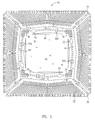
- FIG. 1 is a conventional metal leadframe 10 . Although not shown, several identical leadframes 10 are formed in an array from a single sheet of metal and each leadframe of the array is processed in parallel.
- Leadframe 10 includes a central metal die pad 11 (shown by horizontal hatching) and radiating metal leads 12 adjacent to die pad 11 .
- An opposite end of each lead 12 is connected to the peripheral frame of the leadframe (not shown).
- a dam bar (not shown) also crosses and connects the leads. The frame and dam bar are removed during a trim and form step. The portion of each lead 12 that is within the dashed line is plated with silver. The perimeter of die pad 11 also may be plated.
- a ring of an adhesive polyimide tape 13 (shown by diagonal hatching) crosses and connects each of the leads 12 at a midpoint and serves to stabilize the leads during processing.
- Four tie bars 14 support die pad 11 and connect it to the peripheral dam bar and frame (not shown).
- Five leads 15 are connected to die pad 11 for support. Die pad 11 is downset, as indicated by downset marks 16 on tie bars 14 and leads 15 .
- FIG. 2 An alternative prior art embodiment of a die pad shown is in FIG. 2 .
- Metal die pad 20 is surrounded by a ring 21 .
- Ring 21 is connected by sixteen metal connectors 22 to die pad 20 .
- Tie bars 23 connect die pad 20 to the remainder of the peripheral frame of the leadframe (not shown). This configuration facilitates spacing of the leads (not shown) and provides an encapsulant locking feature.
- the integrated circuit device In a completed package, the integrated circuit device is mounted on the die pad.
- integrated circuit devices require connection to a power voltage source, sometimes denoted “Vdd,” and a ground voltage source, sometimes denoted “Vss.”
- a lead of the package typically is dedicated to supply Vdd.
- a second dedicated lead provides Vss.
- the use of dedicated leads for power and ground voltages limits the flexibility of the package because the user of the package, for example, a chip manufacturer or computer manufacturer, cannot vary which leads are to be used for connection to input and output (“I/O”) signals and which leads are to be used for connection to Vdd and Vss.
- a second dedicated lead provides Vss.
- leads for power and ground voltages limits the flexibility of the package because the user of the package, for example, a chip manufacturer or computer manufacturer, cannot vary which leads are to be used for connection to input and output (“I/O”) signals and which leads are to be used for connection to Vdd and Vss.
- I/O input and output
- the present invention includes a package made from a leadframe having an inventive design.
- the package overcomes the limitations of prior art packages by allowing all leads of the package to be used for either I/O signals or power or ground leads. This allows a common package design to be used even when the location of the power voltage, ground voltage, and I/O signal inputs vary among different electronic devices.
- a leadframe within the present invention includes a central metal die pad.
- a metal ring surrounds the die pad. The metal ring is spaced a small distance apart from the die pad.
- a nonconductive connector is attached between the die pad and the surrounding ring and holds the die pad and the ring together.
- An example nonconductive connector is a polyimide adhesive tape.
- a plurality of leads extend from the periphery of the leadframe toward the die pad and ring. The leads terminate adjacent to the ring. The ring is between the ends of the leads and the die pad. None of the leads directly connect to the ring. In an alternative embodiment, one or more of the leads is directly connected to the ring and provides support for the ring.
- a bypass capacitor or decoupling capacitor is connected between the die pad and the ring and filters the input power voltage.
- the present invention also includes a method for making the leadframe described above.
- Step 1 of the method provides a metal sheet.
- Step 2 patterns the metal sheet to form the die pad, the surrounding ring, and the leads.
- a temporary metal connector or a plurality of temporary metal connectors also are formed from the metal sheet and connect the die pad to the ring.
- Step 3 connects a nonconductive connector, such as polyimide adhesive tape, between the die pad and ring.
- a plurality of nonconductive connectors, such as two or four segments of tape, may be used to connect the die pad and ring.
- Step 4 removes the temporary metal connector(s) so that only the nonconductive connector(s) holds the die pad to the surrounding ring.
- Step 4 can be accomplished using several methods, including punching, etching, or laser cutting methods.
- the tips of the leads and the periphery of the die pad are plated with another metal, such as silver, to facilitate connection to bond wires.
- a bypass, decoupling, or filter capacitor may be connected between the die pad and the surrounding ring. Capacitor connection may be accomplished using a variety of methods, such as conductive adhesive or soft soldering methods.
- a package made from the above-described leadframe includes the metal die pad, surrounding metal ring, nonconductive connector(s), and leads.
- An integrated circuit device is on the die pad.
- the leads are connected by conductors, e.g., bond wires, to conductive pads on the integrated circuit device.
- One of the leads is connected by a bond wire to the ring.
- the ring is connected to the lead that is attached to a power voltage input Vdd.
- the ring in turn is connected by a bond wire to a pad on the integrated circuit device for inputting the power voltage to the integrated circuit device.
- the die pad is isolated from the ring and is floating.
- a lead that attaches to a ground voltage is connected by a bond wire to the die pad.
- a capacitor (filter, bypass, or decoupling) may be connected between the ring and the die pad.
- Hardened encapsulant material covers the entire structure, including the nonconductive connectors and the integrated circuit device.
- Step 1 of the method provides a leadframe having the features described above, including a central die pad, a surrounding ring separated from the die pad, a nonconductive connector holding the die pad to the ring, and radiating leads.
- Step 2 attaches an integrated circuit device to the die pad.
- Step 2 is accomplished using industry standard practices utilizing conductive or nonconductive organic epoxies or polyimides, as well as soft solders and conductive adhesive tapes.
- Step 3 installs conductive connectors between the integrated circuit device and the leads, between one or more of the leads and the ring, and between the ring and the integrated circuit device.
- Step 3 is accomplished using industry standard practices, such as wire bonding using thermosonic, thermo-compression, or ultrasonic wedge methods.
- Step 4 applies an encapsulant material over the entire structure.
- thermoset epoxies are used. These include Epoxidized ortho uresol novolac (“EOCN”), bi-phenyl (“Ep”), dicyclopentadiene (“DCPD”), and multi-functional (“MF”) epoxies.
- EOCN Epoxidized ortho uresol novolac
- Ep bi-phenyl
- DCPD dicyclopentadiene
- MF multi-functional
- FIG. 1 is a top plan view of a prior art leadframe.
- FIG. 2 is a top plan view of a prior art die pad connected by metal connectors to a surrounding metal ring.
- FIG. 3 is a top plan view of a leadframe having a rectangular die pad surrounded by a rectangular ring.
- FIG. 3A is a top plan view of an alternative embodiment of the leadframe of FIG. 3 .
- FIG. 4 is a top plan view of an incomplete leadframe having an octagonal die pad surrounded by an octagonal ring.
- FIG. 4A is a top plan view of an alternative embodiment of the leadframe of FIG. 4 .
- FIG. 5 is a top plan view of the leadframe of FIG. 4 after four nonconductive adhesive tape segments are applied to connect the die pad to the ring.
- FIG. 6 is a top plan view of an alternative embodiment a leadframe having a ring of nonconductive tape between the die pad and surrounding ring.
- FIG. 7 is a cross-sectional side view of a package containing an integrated circuit device.
- FIG. 8 is a plan view of the package of FIG. 7 along line 8 — 8 .
- FIG. 9 is a flow chart of a method of making a leadframe.
- FIG. 10 is a flow chart of a method of making a package.
- FIG. 3 is an embodiment of a leadframe 30 within the present invention.
- FIGS. 7 and 8 show a package 60 for an integrated circuit device.
- Package 60 of FIG. 7 is made from leadframe 30 of FIG. 3 .
- package 60 is discussed first, followed by a discussion of leadframe 30 of FIG. 3 .
- Package 60 of FIG. 7 includes an integrated circuit device 63 attached onto a planar central metal die pad 31 . Adjacent to either side of die pad 31 is a planar metal ring 33 . Die pad 31 and ring 33 are downset. Although not shown in this view, ring 33 surrounds die pad 31 . Segments of a nonconductive adhesive tape 36 connect ring 33 to a peripheral portion of die pad 31 . Tape 36 spans space 35 between die pad 31 and ring 33 . Conductive metal bond wires 61 connect leads 32 to conductive pads 64 on integrated circuit device 63 .
- An insulative, adhesive encapsulant material 62 forms the package body and covers integrated circuit device 63 , die pad 31 , ring 33 , tape 36 , bond wires 61 , and a portion of leads 32 adjacent to ring 33 .
- the segments of nonconductive tape 36 are replaced with a contiguous nonconductive tape that connects the entire perimeter of die pad 31 to ring 33 .
- a different lead 32 for carrying a power voltage Vdd is connected by a bond wire to ring 33
- ring 33 is connected by a separate bond wire to a conductive pad 64 on integrated circuit device 63
- die pad 31 is connected to a different lead 32 carrying a ground voltage Vss.
- one or more leads are directly connected to ring 33 .
- FIG. 8 is a plan view of package 60 of FIG. 7 along line 8 — 8 .
- ring 33 surrounds die pad 31 .
- a space 35 filled by encapsulant material 62 is between die pad 31 and ring 33 .
- Both die pad 31 and ring 33 have a rectangular perimeter.
- the four corners of die pad 31 and ring 33 are juxtaposed.
- the four corners of die pad 31 are each connected by a segment of nonconductive tape 36 (shown with diagonal hatching) to the juxtaposed corner of ring 33 .
- Portions of severed tie bars 34 extend from ring 33 toward the perimeter of package 60 .
- An optional capacitor 39 A is connected between die pad 31 and ring 33 , and acts as a filter between Vdd and Vss when the package is mounted on a printed circuit board and is in operation.
- Package 60 of FIGS. 7 and 8 is formed of conventional materials.
- die pad 31 , ring 33 , and leads 32 are formed of copper, copper alloy, or Alloy 42 .
- the encapsulated tips of leads 32 , ring 33 , and a peripheral portion of die pad 31 may be plated with another conventional metal, such as silver or nickel palladium, to facilitate bond wire connections.
- Nonconductive tape 36 is, for example, a conventional polyimide or polyimide-based tape, which is available from the E.I. Dupont Company of Del. and Circleville, Ohio (United States), or from the Toray Dupont Company of Japan.
- package 60 was formed from leadframe 30 of FIG. 3 .
- Leadframe 30 is a patterned planar metal sheet to which several pieces of a nonconductive adhesive tape have been applied.
- Leadframe 30 of FIG. 3 includes a planar central metal die pad 31 .
- Die pad 31 has a rectangular perimeter including four corners. Adjacent to the corners of die pad 31 is a space 31 A, which provides an encapsulant locking feature in a completed package.
- Die pad 31 of FIG. 3 is surrounded by planar metal ring 33 . (For clarity, die pad 31 and ring 33 have horizontal cross hatches in FIG. 3.) Capacitor 39 A is attached between die pad 31 and ring 33 .
- Ring 33 of FIG. 3 also has a rectangular perimeter, and the four corners of die pad 31 are juxtaposed with the four corners of ring 33 .
- An empty space 35 is present around die pad 31 between die pad 31 and ring 33 .
- An “L” shaped segment of a nonconductive adhesive tape 36 connects a peripheral portion of each of the four corners of die pad 31 to the juxtaposed corner of ring 33 .
- Tie bars 34 extend from the corners of ring 33 and connect ring 33 to the outer frame (not shown) of leadframe 30 .
- Die pad 31 and ring 33 are downset, as indicated by downset marks 38 .
- Each hole 37 represents a point where a temporary metal connector between die pad 31 and ring 33 was removed after tape 36 was applied to connect die pad 31 and ring 33 .
- the location of these temporary connectors can vary. For example, the temporary connectors could be located at the four corners in an alternative embodiment (not shown).
- Leads 32 of leadframe 30 of FIG. 3 extend from the outer frame (not shown) of leadframe 30 toward ring 33 . Leads 32 terminate adjacent to ring 33 , and none of leads 32 contact ring 33 .
- FIG. 3 includes 144 leads, although the number of leads will vary with the application.
- a dam bar (not shown) connects each of leads 32 until a trim and form step.
- a ring of a nonconductive adhesive tape 39 crosses and connects each of leads 32 . Tape 39 stabilizes leads 32 during processing.
- the tips of leads 32 inside the dashed line are plated with silver, nickel palladium, or another common plating metal.
- any one of leads 32 of FIG. 3 may be connected to a voltage source or an I/O signal.
- a lead 32 is identified for connection to a power source Vdd, and that lead is then connected to ring 33 .
- Ring 33 is then connected by a bond wire or equivalent conductor to a power voltage Vdd input pad 64 on integrated circuit device 63 (FIG. 7 ).
- Die pad 31 may or may not be connected to a lead that is in turn connected to a ground voltage source Vss, depending on whether the application calls for connection of die pad 31 to an external ground voltage lead.
- FIG. 3A is an alternative embodiment of a leadframe.
- Leadframe 40 of FIG. 3A is identical to leadframe 30 of FIG. 3 except that ring 33 is directly connected to five downset leads 41 .
- Leads 41 support ring 33 of leadframe 40 .
- none of leads 41 is connected to an input.
- leads 41 only provide support to ring 33 .
- one of leads 41 is identified for connection to the power voltage source Vdd, and a bond wire or equivalent conductor may be used to connect ring 33 to a power input pad on the integrated circuit device.
- FIG. 4 is an incomplete leadframe 42 having an alternative die pad 43 and ring 44 .
- Leadframe 42 is incomplete because four temporary metal connectors 45 connect metal die pad 43 and metal ring 44 .
- temporary connectors 45 are removed after a nonconductive tape is applied to connect die pad 43 to ring 44 .
- the octagonal perimeter shapes of die pad 43 and ring 44 of FIG. 4 facilitate the spacing of leads 32 .
- Die pad 43 of FIG. 4 has a perimeter with eight sides.
- the planar area of die pad 43 includes four spaces 46 , which provide an encapsulant locking capability in a completed package.
- Ring 44 surrounds die pad 43 and has an eight-sided perimeter that matches the perimeter of die pad 43 .
- Space 35 between die pad 43 and ring 44 is spanned by four temporary metal connectors 45 that connect die pad 43 to ring 44 . In subsequent processing, temporary metal connectors 45 are removed.
- Ring 44 is connected to the outer frame (not shown) of leadframe 42 by four tie bars 34 .
- Downset marks 38 show that die pad 43 and ring 44 are downset.
- Leads 32 extend from the outer frame (not shown) of leadframe 42 toward ring 44 . No leads 32 directly contact ring 44 .
- temporary metal connectors 45 is varied.
- temporary connectors may be located at the juxtaposed corners of die pad 43 and ring 44 where the four tie bars 34 directly connect to ring 44 .
- FIG. 4A is an incomplete leadframe 50 .
- Leadframe 50 of FIG. 4A is identical to leadframe 42 of FIG. 4 except that ring 44 is directly connected to five leads 51 .
- Leads 51 support ring 44 .
- leads 51 may or may not be connected to a power voltage input Vdd, as described above for FIG. 3 A.
- FIG. 5 shows leadframe 42 of FIG. 4 at a later stage of processing.
- four segments of a nonconductive tape 36 (shown by diagonal hatching) are attached to and connect four juxtaposed corners of metal die pad 43 and metal ring 44 .
- Four holes 52 are between die pad 43 and ring 44 . Holes 52 were made after nonconductive tape 36 was applied by punching out or otherwise removing temporary metal connectors 45 of FIG. 4 .
- Four capacitors 39 A are attached in a symmetrical fashion between die pad 43 and ring 44 . More capacitors 39 A can be accommodated based on the capacitance requirement and space limitations.
- a ring of polyimide tape may be applied across all of leads 32 , similar to tape 39 of FIG. 3, to stabilize leads 32 during processing.
- FIG. 6 shows an alternative completed leadframe 54 .
- Leadframe 54 is identical to leadframe 42 of FIG. 5 except for the configuration of the nonconductive tape that connects the peripheral portion of die pad 43 to surrounding ring 44 .
- a ring of nonconductive tape 55 instead of four segments of a nonconductive tape 46 at juxtaposed corners, a ring of nonconductive tape 55 having the same perimeter shape as die pad 43 and ring 44 is attached between die pad 43 and ring 44 around their entire juxtaposed perimeters. Tape 55 is shown by diagonal cross hatching.
- holes 52 are made by punching through tape 55 to remove temporary metal connectors 45 .
- FIG. 9 is a method within the present invention of making a leadframe such as leadframe 30 of FIG. 3, leadframe 40 of FIG. 3A, leadframe 42 of FIG. 5, and leadframe 54 of FIG. 6 .
- Step 1 of the method of FIG. 9 provides a thin metal sheet.
- the metal sheet may be formed of any metal or metals conventionally used for making leadframes, such as copper, copper alloys, or Alloy 42 .
- Step 2 of FIG. 9 patterns the metal sheet to form the metal portions of leadframe 42 of FIG. 4, including die pad 43 , surrounding ring 44 , tie bars 34 , leads 32 , and temporary connectors 45 . Portions of leadframe 42 may be downset or plated.
- Step 2 uses conventional patterning methods.
- Example patterning methods include etching the metal sheet using a liquid enchant and a photoresist mask, or progressive metal stamping.
- an array of leadframes will be formed from a single metal sheet and processed simultaneously. The end result is a metal strip including an array of identical leadframes that can undergo subsequent assembly in parallel.
- Step 3 of FIG. 9 attaches a nonconductive connector, such as polyimide adhesive tape, to a peripheral portion of die pad 43 and to ring 44 .
- the tape should overlap enough of the peripheral portion of die pad 43 and the width of ring 44 to provide a secure connection between die pad 43 and ring 44 .
- four tape segments 45 are stamped onto or otherwise applied to four juxtaposed corners of die pad 43 and ring 44 .
- Some balancing of the amount of tape and package performance is required. Greater amounts of tape (such as in FIG. 6) provide greater attachment and stability, but may cause the package to absorb greater amounts of moisture.
- a ring of tape also may be applied across leads 32 , along the lines of tape 39 of FIG. 3 .
- Step 4 of FIG. 9 removes the temporary metal connectors that hold die pad 43 to ring 44 .
- this step is performed by punching out temporary connectors 45 .
- Step 4 can be accomplished by etching or laser cutting methods. At the completion of this step, only the four segments of nonconductive tape 36 hold die pad 43 to ring 44 .
- Step 4 requires punching or otherwise piercing through tape segments 36 .
- capacitors 39 A are connected between die pad 43 and ring 44 , depending on the requirements of the package.
- the capacitors may be any variety of sizes, based on the capacitance required and space available.
- a common size for this application has a 0402 body size.
- FIG. 10 is a flow chart of a method within the present invention of making a package using the above described leadframes.
- FIGS. 7 and 8 show a package made by the process.
- Step 1 of FIG. 10 provides a leadframe having the features exemplified in FIGS. 3, 5 , or 6 .
- Step 1 provides a leadframe 30 .
- leadframe 30 includes a central metal die pad 31 and a metal ring 33 that surrounds die pad 31 and is spaced apart from die pad 31 by a space 35 .
- Leadframe 30 also includes four segments of a nonconductive connection tape 36 that connect peripheral portions of die pad 31 to ring 33 .
- Leadframe 30 also includes a plurality of leads 32 that begin adjacent to ring 33 and terminate at the periphery of the leadframe.
- Step 2 of FIG. 10 attaches an integrated circuit device 63 to die pad 31 .
- Conventional die attach equipment, adhesives, and methods can be used.
- Conventional die attach equipment, adhesives, and methods can be used.
- Step 3 installs conductive connectors, such as bond wires or equivalent, between the integrated circuit device and the components of the leadframe.
- Conventional wire bonding methods can be used. For example, referring to FIGS. 3 and 7, a bond wire is connected between a lead 32 and ring 33 to provide input power voltage Vdd to ring 33 . Another bond wire is connected between ring 33 and a Vdd input pad on integrated circuit device 63 . Other leads are connected by bond wires 61 to I/O signal pads on integrated circuit device 63 .
- the potential of die pad 31 may float, or a bond wire may be used to connect die pad 31 to a lead 32 that is to be connected to an external ground voltage.
- Step 4 of FIG. 10 applies an insulative, adhesive encapsulant material over the entire structure.
- encapsulant material 62 covers integrated circuit device 63 , bond wires 61 , die pad 31 , ring 33 , nonconductive adhesive tape 36 , and the portion of leads 32 adjacent to ring 33 .
- Conventional encapsulation techniques such as transfer or injection molding, are used.
- Conventional encapsulant materials such as epoxy resins, are used.
- Step 5 of FIG. 10 hardens the encapsulant material by conventional methods, such as heating.
- Step 6 of FIG. 10 trims and forms the encapsulated package. If a plurality of packages are processed simultaneously using an array of leadframes, then individual packages must be separated from the array. Sawing or punching to separate the packages may be used.
- the embodiments described herein are merely examples of the present invention. Artisans will appreciate that variations are possible within the scope of the claims.
Abstract
Description
Claims (45)
Priority Applications (1)
| Application Number | Priority Date | Filing Date | Title |
|---|---|---|---|
| US09/593,269 US6339252B1 (en) | 1999-08-09 | 2000-06-13 | Electronic device package and leadframe |
Applications Claiming Priority (2)
| Application Number | Priority Date | Filing Date | Title |
|---|---|---|---|
| US09/370,600 US6258629B1 (en) | 1999-08-09 | 1999-08-09 | Electronic device package and leadframe and method for making the package |
| US09/593,269 US6339252B1 (en) | 1999-08-09 | 2000-06-13 | Electronic device package and leadframe |
Related Parent Applications (1)
| Application Number | Title | Priority Date | Filing Date |
|---|---|---|---|
| US09/370,600 Division US6258629B1 (en) | 1999-08-09 | 1999-08-09 | Electronic device package and leadframe and method for making the package |
Publications (1)
| Publication Number | Publication Date |
|---|---|
| US6339252B1 true US6339252B1 (en) | 2002-01-15 |
Family
ID=23460339
Family Applications (2)
| Application Number | Title | Priority Date | Filing Date |
|---|---|---|---|
| US09/370,600 Expired - Lifetime US6258629B1 (en) | 1999-08-09 | 1999-08-09 | Electronic device package and leadframe and method for making the package |
| US09/593,269 Expired - Lifetime US6339252B1 (en) | 1999-08-09 | 2000-06-13 | Electronic device package and leadframe |
Family Applications Before (1)
| Application Number | Title | Priority Date | Filing Date |
|---|---|---|---|
| US09/370,600 Expired - Lifetime US6258629B1 (en) | 1999-08-09 | 1999-08-09 | Electronic device package and leadframe and method for making the package |
Country Status (1)
| Country | Link |
|---|---|
| US (2) | US6258629B1 (en) |
Cited By (42)
| Publication number | Priority date | Publication date | Assignee | Title |
|---|---|---|---|---|
| US20020056894A1 (en) * | 2000-10-16 | 2002-05-16 | Frank Kuo | Leadframe having slots in a die pad |
| US20020140061A1 (en) * | 2001-03-27 | 2002-10-03 | Lee Hyung Ju | Lead frame for semiconductor package |
| US6660559B1 (en) | 2001-06-25 | 2003-12-09 | Amkor Technology, Inc. | Method of making a chip carrier package using laser ablation |
| US20040053447A1 (en) * | 2001-06-29 | 2004-03-18 | Foster Donald Craig | Leadframe having fine pitch bond fingers formed using laser cutting method |
| US20050026386A1 (en) * | 2002-04-19 | 2005-02-03 | Micron Technology, Inc. | Ultrathin leadframe BGA circuit package |
| US20050098862A1 (en) * | 2001-07-30 | 2005-05-12 | Nec Electronics Corporation | Lead frame and semiconductor device having the same as well as method of resin-molding the same |
| US20050248016A1 (en) * | 2004-05-05 | 2005-11-10 | Cheng-Yen Huang | Chip-packaging with bonding options having a plurality of package substrates |
| US20080073784A1 (en) * | 2006-09-27 | 2008-03-27 | Samsung Electronics Co., Ltd. | Circuit substrate for preventing warpage and package using the same |
| US20090014851A1 (en) * | 2007-07-10 | 2009-01-15 | Choi Yeonho | Fusion quad flat semiconductor package |
| US20090096063A1 (en) * | 2001-04-06 | 2009-04-16 | Oki Electric Industry Co., Ltd. | Semiconductor apparatus with decoupling capacitor |
| US20090224380A1 (en) * | 2008-03-04 | 2009-09-10 | Powertech Technology Inc. | Leadframe and semiconductor package having downset baffle paddles |
| WO2010011206A1 (en) * | 2008-07-25 | 2010-01-28 | Delphi Technologies, Inc. | Slot card crash sensor and method |
| US7732899B1 (en) | 2005-12-02 | 2010-06-08 | Amkor Technology, Inc. | Etch singulated semiconductor package |
| US7808084B1 (en) | 2008-05-06 | 2010-10-05 | Amkor Technology, Inc. | Semiconductor package with half-etched locking features |
| US7847392B1 (en) | 2008-09-30 | 2010-12-07 | Amkor Technology, Inc. | Semiconductor device including leadframe with increased I/O |
| US7875963B1 (en) | 2008-11-21 | 2011-01-25 | Amkor Technology, Inc. | Semiconductor device including leadframe having power bars and increased I/O |
| US7960818B1 (en) | 2009-03-04 | 2011-06-14 | Amkor Technology, Inc. | Conformal shield on punch QFN semiconductor package |
| US7968998B1 (en) | 2006-06-21 | 2011-06-28 | Amkor Technology, Inc. | Side leaded, bottom exposed pad and bottom exposed lead fusion quad flat semiconductor package |
| US7982298B1 (en) | 2008-12-03 | 2011-07-19 | Amkor Technology, Inc. | Package in package semiconductor device |
| US20110180915A1 (en) * | 2010-01-26 | 2011-07-28 | Denso Corporation | Electronic device and method of manufacturing the same |
| US7989933B1 (en) | 2008-10-06 | 2011-08-02 | Amkor Technology, Inc. | Increased I/O leadframe and semiconductor device including same |
| US8008758B1 (en) | 2008-10-27 | 2011-08-30 | Amkor Technology, Inc. | Semiconductor device with increased I/O leadframe |
| US8026589B1 (en) | 2009-02-23 | 2011-09-27 | Amkor Technology, Inc. | Reduced profile stackable semiconductor package |
| US8058715B1 (en) | 2009-01-09 | 2011-11-15 | Amkor Technology, Inc. | Package in package device for RF transceiver module |
| US8067821B1 (en) | 2008-04-10 | 2011-11-29 | Amkor Technology, Inc. | Flat semiconductor package with half package molding |
| US8072050B1 (en) | 2008-11-18 | 2011-12-06 | Amkor Technology, Inc. | Semiconductor device with increased I/O leadframe including passive device |
| US8089145B1 (en) | 2008-11-17 | 2012-01-03 | Amkor Technology, Inc. | Semiconductor device including increased capacity leadframe |
| US8184453B1 (en) | 2008-07-31 | 2012-05-22 | Amkor Technology, Inc. | Increased capacity semiconductor package |
| US8318287B1 (en) | 1998-06-24 | 2012-11-27 | Amkor Technology, Inc. | Integrated circuit package and method of making the same |
| US8487420B1 (en) | 2008-12-08 | 2013-07-16 | Amkor Technology, Inc. | Package in package semiconductor device with film over wire |
| US8575742B1 (en) | 2009-04-06 | 2013-11-05 | Amkor Technology, Inc. | Semiconductor device with increased I/O leadframe including power bars |
| US8648450B1 (en) | 2011-01-27 | 2014-02-11 | Amkor Technology, Inc. | Semiconductor device including leadframe with a combination of leads and lands |
| US8680656B1 (en) | 2009-01-05 | 2014-03-25 | Amkor Technology, Inc. | Leadframe structure for concentrated photovoltaic receiver package |
| CN103682030A (en) * | 2012-09-07 | 2014-03-26 | 深圳市龙岗区横岗光台电子厂 | LED, LED device and LED manufacture technology |
| US8729710B1 (en) | 2008-01-16 | 2014-05-20 | Amkor Technology, Inc. | Semiconductor package with patterning layer and method of making same |
| US8754513B1 (en) * | 2008-07-10 | 2014-06-17 | Marvell International Ltd. | Lead frame apparatus and method for improved wire bonding |
| US9184148B2 (en) | 2013-10-24 | 2015-11-10 | Amkor Technology, Inc. | Semiconductor package and method therefor |
| US9184118B2 (en) | 2013-05-02 | 2015-11-10 | Amkor Technology Inc. | Micro lead frame structure having reinforcing portions and method |
| US9631481B1 (en) | 2011-01-27 | 2017-04-25 | Amkor Technology, Inc. | Semiconductor device including leadframe with a combination of leads and lands and method |
| US9673122B2 (en) | 2014-05-02 | 2017-06-06 | Amkor Technology, Inc. | Micro lead frame structure having reinforcing portions and method |
| US9704725B1 (en) | 2012-03-06 | 2017-07-11 | Amkor Technology, Inc. | Semiconductor device with leadframe configured to facilitate reduced burr formation |
| US10811341B2 (en) | 2009-01-05 | 2020-10-20 | Amkor Technology Singapore Holding Pte Ltd. | Semiconductor device with through-mold via |
Families Citing this family (57)
| Publication number | Priority date | Publication date | Assignee | Title |
|---|---|---|---|---|
| KR20010037247A (en) * | 1999-10-15 | 2001-05-07 | 마이클 디. 오브라이언 | Semiconductor package |
| JP2001156237A (en) * | 1999-11-25 | 2001-06-08 | Mitsubishi Electric Corp | Lead frame and resin-sealed semiconductor device using it |
| US7042068B2 (en) | 2000-04-27 | 2006-05-09 | Amkor Technology, Inc. | Leadframe and semiconductor package made using the leadframe |
| US7034382B2 (en) * | 2001-04-16 | 2006-04-25 | M/A-Com, Inc. | Leadframe-based chip scale package |
| JP3476442B2 (en) * | 2001-05-15 | 2003-12-10 | 沖電気工業株式会社 | Semiconductor device and manufacturing method thereof |
| US6734552B2 (en) | 2001-07-11 | 2004-05-11 | Asat Limited | Enhanced thermal dissipation integrated circuit package |
| US7015072B2 (en) | 2001-07-11 | 2006-03-21 | Asat Limited | Method of manufacturing an enhanced thermal dissipation integrated circuit package |
| US7126218B1 (en) | 2001-08-07 | 2006-10-24 | Amkor Technology, Inc. | Embedded heat spreader ball grid array |
| US6790710B2 (en) * | 2002-01-31 | 2004-09-14 | Asat Limited | Method of manufacturing an integrated circuit package |
| US6686651B1 (en) | 2001-11-27 | 2004-02-03 | Amkor Technology, Inc. | Multi-layer leadframe structure |
| US6737750B1 (en) | 2001-12-07 | 2004-05-18 | Amkor Technology, Inc. | Structures for improving heat dissipation in stacked semiconductor packages |
| US20030178719A1 (en) * | 2002-03-22 | 2003-09-25 | Combs Edward G. | Enhanced thermal dissipation integrated circuit package and method of manufacturing enhanced thermal dissipation integrated circuit package |
| US6608366B1 (en) | 2002-04-15 | 2003-08-19 | Harry J. Fogelson | Lead frame with plated end leads |
| US6940154B2 (en) * | 2002-06-24 | 2005-09-06 | Asat Limited | Integrated circuit package and method of manufacturing the integrated circuit package |
| US6905914B1 (en) | 2002-11-08 | 2005-06-14 | Amkor Technology, Inc. | Wafer level package and fabrication method |
| US7723210B2 (en) | 2002-11-08 | 2010-05-25 | Amkor Technology, Inc. | Direct-write wafer level chip scale package |
| KR100568224B1 (en) * | 2003-11-04 | 2006-04-07 | 삼성전자주식회사 | Tape circuit substrate and semiconductor apparatus employing the same |
| US7572681B1 (en) | 2005-12-08 | 2009-08-11 | Amkor Technology, Inc. | Embedded electronic component package |
| US7902660B1 (en) | 2006-05-24 | 2011-03-08 | Amkor Technology, Inc. | Substrate for semiconductor device and manufacturing method thereof |
| US8294248B2 (en) * | 2006-11-30 | 2012-10-23 | Marvell World Trade Ltd. | Chip on leads |
| US9082607B1 (en) | 2006-12-14 | 2015-07-14 | Utac Thai Limited | Molded leadframe substrate semiconductor package |
| US7687893B2 (en) | 2006-12-27 | 2010-03-30 | Amkor Technology, Inc. | Semiconductor package having leadframe with exposed anchor pads |
| US7829990B1 (en) | 2007-01-18 | 2010-11-09 | Amkor Technology, Inc. | Stackable semiconductor package including laminate interposer |
| US7982297B1 (en) | 2007-03-06 | 2011-07-19 | Amkor Technology, Inc. | Stackable semiconductor package having partially exposed semiconductor die and method of fabricating the same |
| US8258609B2 (en) * | 2007-03-21 | 2012-09-04 | Stats Chippac Ltd. | Integrated circuit package system with lead support |
| US7687899B1 (en) | 2007-08-07 | 2010-03-30 | Amkor Technology, Inc. | Dual laminate package structure with embedded elements |
| US7777351B1 (en) | 2007-10-01 | 2010-08-17 | Amkor Technology, Inc. | Thin stacked interposer package |
| US8089159B1 (en) | 2007-10-03 | 2012-01-03 | Amkor Technology, Inc. | Semiconductor package with increased I/O density and method of making the same |
| US7847386B1 (en) | 2007-11-05 | 2010-12-07 | Amkor Technology, Inc. | Reduced size stacked semiconductor package and method of making the same |
| US7737537B2 (en) * | 2007-12-12 | 2010-06-15 | Infineon Technologies Ag | Electronic device |
| US7723852B1 (en) | 2008-01-21 | 2010-05-25 | Amkor Technology, Inc. | Stacked semiconductor package and method of making same |
| US7768135B1 (en) | 2008-04-17 | 2010-08-03 | Amkor Technology, Inc. | Semiconductor package with fast power-up cycle and method of making same |
| US8125064B1 (en) | 2008-07-28 | 2012-02-28 | Amkor Technology, Inc. | Increased I/O semiconductor package and method of making same |
| US9113547B2 (en) * | 2008-10-24 | 2015-08-18 | Intel Corporation | Same layer microelectronic circuit patterning using hybrid laser projection patterning (LPP) and semi-additive patterning(SAP) |
| US8796561B1 (en) | 2009-10-05 | 2014-08-05 | Amkor Technology, Inc. | Fan out build up substrate stackable package and method |
| US8937381B1 (en) | 2009-12-03 | 2015-01-20 | Amkor Technology, Inc. | Thin stackable package and method |
| US9355940B1 (en) * | 2009-12-04 | 2016-05-31 | Utac Thai Limited | Auxiliary leadframe member for stabilizing the bond wire process |
| US9691734B1 (en) | 2009-12-07 | 2017-06-27 | Amkor Technology, Inc. | Method of forming a plurality of electronic component packages |
| US8324511B1 (en) | 2010-04-06 | 2012-12-04 | Amkor Technology, Inc. | Through via nub reveal method and structure |
| US8294276B1 (en) | 2010-05-27 | 2012-10-23 | Amkor Technology, Inc. | Semiconductor device and fabricating method thereof |
| CN102332441B (en) * | 2010-07-12 | 2014-05-14 | 无锡华润安盛科技有限公司 | High-alignment-packaging-type lead frame and packaging structure thereof |
| US8440554B1 (en) | 2010-08-02 | 2013-05-14 | Amkor Technology, Inc. | Through via connected backside embedded circuit features structure and method |
| US8487445B1 (en) | 2010-10-05 | 2013-07-16 | Amkor Technology, Inc. | Semiconductor device having through electrodes protruding from dielectric layer |
| US8791501B1 (en) | 2010-12-03 | 2014-07-29 | Amkor Technology, Inc. | Integrated passive device structure and method |
| US8674485B1 (en) | 2010-12-08 | 2014-03-18 | Amkor Technology, Inc. | Semiconductor device including leadframe with downsets |
| US8390130B1 (en) | 2011-01-06 | 2013-03-05 | Amkor Technology, Inc. | Through via recessed reveal structure and method |
| JP5582040B2 (en) * | 2011-01-12 | 2014-09-03 | 富士電機株式会社 | Semiconductor device manufacturing method, semiconductor device, and igniter device |
| US10211134B2 (en) | 2011-09-30 | 2019-02-19 | Mediatek Inc. | Semiconductor package |
| US8941221B2 (en) | 2011-09-30 | 2015-01-27 | Mediatek Inc. | Semiconductor package |
| US9852966B2 (en) | 2011-09-30 | 2017-12-26 | Mediatek Inc. | Semiconductor package |
| US8552548B1 (en) | 2011-11-29 | 2013-10-08 | Amkor Technology, Inc. | Conductive pad on protruding through electrode semiconductor device |
| CN103137593A (en) * | 2011-12-02 | 2013-06-05 | 无锡华润安盛科技有限公司 | Lead frame for packaging integrated circuit and corresponding packaging components |
| US9129943B1 (en) | 2012-03-29 | 2015-09-08 | Amkor Technology, Inc. | Embedded component package and fabrication method |
| US9048298B1 (en) | 2012-03-29 | 2015-06-02 | Amkor Technology, Inc. | Backside warpage control structure and fabrication method |
| US8633575B1 (en) * | 2012-05-24 | 2014-01-21 | Amkor Technology, Inc. | IC package with integrated electrostatic discharge protection |
| US8933547B1 (en) * | 2013-11-21 | 2015-01-13 | Freescale Semiconductor, Inc. | Lead frame with power bar for semiconductor device |
| TWI570858B (en) * | 2014-12-23 | 2017-02-11 | 揚智科技股份有限公司 | Semiconductor package structure |
Citations (8)
| Publication number | Priority date | Publication date | Assignee | Title |
|---|---|---|---|---|
| DE4021872A1 (en) * | 1990-07-09 | 1992-01-23 | Lsi Logic Products Gmbh | Highly integrated electronic component with semiconductor chip - stabilises terminal lead frame by insulating strip-form frame with slits joining conductor paths by conductive adhesive |
| EP0503201A2 (en) * | 1990-12-20 | 1992-09-16 | Kabushiki Kaisha Toshiba | Semiconductor device having an interconnecting circuit board and method for manufacturing same |
| US5328870A (en) | 1992-01-17 | 1994-07-12 | Amkor Electronics, Inc. | Method for forming plastic molded package with heat sink for integrated circuit devices |
| US5332864A (en) * | 1991-12-27 | 1994-07-26 | Vlsi Technology, Inc. | Integrated circuit package having an interposer |
| US5336927A (en) * | 1992-02-03 | 1994-08-09 | Nec Corporation | Lead frame having electrically insulating tapes adhered to the inner leads |
| US5451812A (en) * | 1991-10-02 | 1995-09-19 | Seiko Epson Corporation | Leadframe for semiconductor devices |
| US5604376A (en) | 1994-06-30 | 1997-02-18 | Digital Equipment Corporation | Paddleless molded plastic semiconductor chip package |
| US5723899A (en) | 1994-08-30 | 1998-03-03 | Amkor Electronics, Inc. | Semiconductor lead frame having connection bar and guide rings |
Family Cites Families (2)
| Publication number | Priority date | Publication date | Assignee | Title |
|---|---|---|---|---|
| US4771330A (en) * | 1987-05-13 | 1988-09-13 | Lsi Logic Corporation | Wire bonds and electrical contacts of an integrated circuit device |
| JPH02201948A (en) * | 1989-01-30 | 1990-08-10 | Toshiba Corp | Package of semiconductor device |
-
1999
- 1999-08-09 US US09/370,600 patent/US6258629B1/en not_active Expired - Lifetime
-
2000
- 2000-06-13 US US09/593,269 patent/US6339252B1/en not_active Expired - Lifetime
Patent Citations (8)
| Publication number | Priority date | Publication date | Assignee | Title |
|---|---|---|---|---|
| DE4021872A1 (en) * | 1990-07-09 | 1992-01-23 | Lsi Logic Products Gmbh | Highly integrated electronic component with semiconductor chip - stabilises terminal lead frame by insulating strip-form frame with slits joining conductor paths by conductive adhesive |
| EP0503201A2 (en) * | 1990-12-20 | 1992-09-16 | Kabushiki Kaisha Toshiba | Semiconductor device having an interconnecting circuit board and method for manufacturing same |
| US5451812A (en) * | 1991-10-02 | 1995-09-19 | Seiko Epson Corporation | Leadframe for semiconductor devices |
| US5332864A (en) * | 1991-12-27 | 1994-07-26 | Vlsi Technology, Inc. | Integrated circuit package having an interposer |
| US5328870A (en) | 1992-01-17 | 1994-07-12 | Amkor Electronics, Inc. | Method for forming plastic molded package with heat sink for integrated circuit devices |
| US5336927A (en) * | 1992-02-03 | 1994-08-09 | Nec Corporation | Lead frame having electrically insulating tapes adhered to the inner leads |
| US5604376A (en) | 1994-06-30 | 1997-02-18 | Digital Equipment Corporation | Paddleless molded plastic semiconductor chip package |
| US5723899A (en) | 1994-08-30 | 1998-03-03 | Amkor Electronics, Inc. | Semiconductor lead frame having connection bar and guide rings |
Cited By (81)
| Publication number | Priority date | Publication date | Assignee | Title |
|---|---|---|---|---|
| US8318287B1 (en) | 1998-06-24 | 2012-11-27 | Amkor Technology, Inc. | Integrated circuit package and method of making the same |
| US8963301B1 (en) | 1998-06-24 | 2015-02-24 | Amkor Technology, Inc. | Integrated circuit package and method of making the same |
| US9224676B1 (en) | 1998-06-24 | 2015-12-29 | Amkor Technology, Inc. | Integrated circuit package and method of making the same |
| US8853836B1 (en) | 1998-06-24 | 2014-10-07 | Amkor Technology, Inc. | Integrated circuit package and method of making the same |
| US6744119B2 (en) * | 2000-10-16 | 2004-06-01 | Siliconix (Taiwan) Ltd. | Leadframe having slots in a die pad |
| US20020056894A1 (en) * | 2000-10-16 | 2002-05-16 | Frank Kuo | Leadframe having slots in a die pad |
| US20020140061A1 (en) * | 2001-03-27 | 2002-10-03 | Lee Hyung Ju | Lead frame for semiconductor package |
| US6713322B2 (en) * | 2001-03-27 | 2004-03-30 | Amkor Technology, Inc. | Lead frame for semiconductor package |
| US20090166842A1 (en) * | 2001-03-27 | 2009-07-02 | Hyung Ju Lee | Leadframe for semiconductor package |
| US7928542B2 (en) | 2001-03-27 | 2011-04-19 | Amkor Technology, Inc. | Lead frame for semiconductor package |
| US8102037B2 (en) | 2001-03-27 | 2012-01-24 | Amkor Technology, Inc. | Leadframe for semiconductor package |
| US20090096063A1 (en) * | 2001-04-06 | 2009-04-16 | Oki Electric Industry Co., Ltd. | Semiconductor apparatus with decoupling capacitor |
| US8018055B2 (en) | 2001-04-06 | 2011-09-13 | Oki Electric Industry Co., Ltd. | Semiconductor apparatus with decoupling capacitor |
| US20100207244A1 (en) * | 2001-04-06 | 2010-08-19 | Oki Electric Industry Co., Ltd. | Semiconductor apparatus with decoupling capacitor |
| US7714434B2 (en) * | 2001-04-06 | 2010-05-11 | Oki Electric Industry Co., Ltd. | Semiconductor apparatus with decoupling capacitor |
| US6660559B1 (en) | 2001-06-25 | 2003-12-09 | Amkor Technology, Inc. | Method of making a chip carrier package using laser ablation |
| US20040053447A1 (en) * | 2001-06-29 | 2004-03-18 | Foster Donald Craig | Leadframe having fine pitch bond fingers formed using laser cutting method |
| US7239009B2 (en) | 2001-07-30 | 2007-07-03 | Nec Corporation | Lead frame and semiconductor device having the same as well as method of resin-molding the same |
| US6894370B2 (en) * | 2001-07-30 | 2005-05-17 | Nec Electronics Corporation | Lead frame and semiconductor device having the same as well as method of resin-molding the same |
| US20050098862A1 (en) * | 2001-07-30 | 2005-05-12 | Nec Electronics Corporation | Lead frame and semiconductor device having the same as well as method of resin-molding the same |
| US7183134B2 (en) | 2002-04-19 | 2007-02-27 | Micron Technology, Inc. | Ultrathin leadframe BGA circuit package |
| US20070099344A1 (en) * | 2002-04-19 | 2007-05-03 | Micron Technology, Inc. | Ultrathin leadframe BGA circuit package |
| US7294911B2 (en) * | 2002-04-19 | 2007-11-13 | Micron Technology, Inc. | Ultrathin leadframe BGA circuit package |
| US20050026386A1 (en) * | 2002-04-19 | 2005-02-03 | Micron Technology, Inc. | Ultrathin leadframe BGA circuit package |
| US20060197208A1 (en) * | 2004-05-05 | 2006-09-07 | Cheng-Yen Huang | Chip-packaging with bonding options having a plurality of package substrates |
| US20050248016A1 (en) * | 2004-05-05 | 2005-11-10 | Cheng-Yen Huang | Chip-packaging with bonding options having a plurality of package substrates |
| US7701041B2 (en) | 2004-05-05 | 2010-04-20 | Faraday Technology Corp. | Chip-packaging with bonding options having a plurality of package substrates |
| US7196401B2 (en) * | 2004-05-05 | 2007-03-27 | Faraday Technology Corp. | Chip-packaging with bonding options having a plurality of package substrates |
| US7732899B1 (en) | 2005-12-02 | 2010-06-08 | Amkor Technology, Inc. | Etch singulated semiconductor package |
| US8441110B1 (en) | 2006-06-21 | 2013-05-14 | Amkor Technology, Inc. | Side leaded, bottom exposed pad and bottom exposed lead fusion quad flat semiconductor package |
| US7968998B1 (en) | 2006-06-21 | 2011-06-28 | Amkor Technology, Inc. | Side leaded, bottom exposed pad and bottom exposed lead fusion quad flat semiconductor package |
| US8014154B2 (en) * | 2006-09-27 | 2011-09-06 | Samsung Electronics Co., Ltd. | Circuit substrate for preventing warpage and package using the same |
| US20080073784A1 (en) * | 2006-09-27 | 2008-03-27 | Samsung Electronics Co., Ltd. | Circuit substrate for preventing warpage and package using the same |
| US8304866B1 (en) | 2007-07-10 | 2012-11-06 | Amkor Technology, Inc. | Fusion quad flat semiconductor package |
| US7977774B2 (en) | 2007-07-10 | 2011-07-12 | Amkor Technology, Inc. | Fusion quad flat semiconductor package |
| US20090014851A1 (en) * | 2007-07-10 | 2009-01-15 | Choi Yeonho | Fusion quad flat semiconductor package |
| US8729710B1 (en) | 2008-01-16 | 2014-05-20 | Amkor Technology, Inc. | Semiconductor package with patterning layer and method of making same |
| US20090224380A1 (en) * | 2008-03-04 | 2009-09-10 | Powertech Technology Inc. | Leadframe and semiconductor package having downset baffle paddles |
| US7812430B2 (en) * | 2008-03-04 | 2010-10-12 | Powertech Technology Inc. | Leadframe and semiconductor package having downset baffle paddles |
| US8067821B1 (en) | 2008-04-10 | 2011-11-29 | Amkor Technology, Inc. | Flat semiconductor package with half package molding |
| US7808084B1 (en) | 2008-05-06 | 2010-10-05 | Amkor Technology, Inc. | Semiconductor package with half-etched locking features |
| US8754513B1 (en) * | 2008-07-10 | 2014-06-17 | Marvell International Ltd. | Lead frame apparatus and method for improved wire bonding |
| US9202797B1 (en) | 2008-07-10 | 2015-12-01 | Marvell International Ltd. | Lead frame apparatus and method for improved wire bonding |
| WO2010011206A1 (en) * | 2008-07-25 | 2010-01-28 | Delphi Technologies, Inc. | Slot card crash sensor and method |
| US8184453B1 (en) | 2008-07-31 | 2012-05-22 | Amkor Technology, Inc. | Increased capacity semiconductor package |
| US8299602B1 (en) | 2008-09-30 | 2012-10-30 | Amkor Technology, Inc. | Semiconductor device including leadframe with increased I/O |
| US7847392B1 (en) | 2008-09-30 | 2010-12-07 | Amkor Technology, Inc. | Semiconductor device including leadframe with increased I/O |
| US8432023B1 (en) * | 2008-10-06 | 2013-04-30 | Amkor Technology, Inc. | Increased I/O leadframe and semiconductor device including same |
| US7989933B1 (en) | 2008-10-06 | 2011-08-02 | Amkor Technology, Inc. | Increased I/O leadframe and semiconductor device including same |
| US8008758B1 (en) | 2008-10-27 | 2011-08-30 | Amkor Technology, Inc. | Semiconductor device with increased I/O leadframe |
| US8823152B1 (en) | 2008-10-27 | 2014-09-02 | Amkor Technology, Inc. | Semiconductor device with increased I/O leadframe |
| US8089145B1 (en) | 2008-11-17 | 2012-01-03 | Amkor Technology, Inc. | Semiconductor device including increased capacity leadframe |
| US8072050B1 (en) | 2008-11-18 | 2011-12-06 | Amkor Technology, Inc. | Semiconductor device with increased I/O leadframe including passive device |
| US8188579B1 (en) | 2008-11-21 | 2012-05-29 | Amkor Technology, Inc. | Semiconductor device including leadframe having power bars and increased I/O |
| US7875963B1 (en) | 2008-11-21 | 2011-01-25 | Amkor Technology, Inc. | Semiconductor device including leadframe having power bars and increased I/O |
| US7982298B1 (en) | 2008-12-03 | 2011-07-19 | Amkor Technology, Inc. | Package in package semiconductor device |
| US8487420B1 (en) | 2008-12-08 | 2013-07-16 | Amkor Technology, Inc. | Package in package semiconductor device with film over wire |
| US8680656B1 (en) | 2009-01-05 | 2014-03-25 | Amkor Technology, Inc. | Leadframe structure for concentrated photovoltaic receiver package |
| US11869829B2 (en) | 2009-01-05 | 2024-01-09 | Amkor Technology Singapore Holding Pte. Ltd. | Semiconductor device with through-mold via |
| US10811341B2 (en) | 2009-01-05 | 2020-10-20 | Amkor Technology Singapore Holding Pte Ltd. | Semiconductor device with through-mold via |
| US8558365B1 (en) | 2009-01-09 | 2013-10-15 | Amkor Technology, Inc. | Package in package device for RF transceiver module |
| US8058715B1 (en) | 2009-01-09 | 2011-11-15 | Amkor Technology, Inc. | Package in package device for RF transceiver module |
| US8026589B1 (en) | 2009-02-23 | 2011-09-27 | Amkor Technology, Inc. | Reduced profile stackable semiconductor package |
| US8729682B1 (en) | 2009-03-04 | 2014-05-20 | Amkor Technology, Inc. | Conformal shield on punch QFN semiconductor package |
| US7960818B1 (en) | 2009-03-04 | 2011-06-14 | Amkor Technology, Inc. | Conformal shield on punch QFN semiconductor package |
| US8575742B1 (en) | 2009-04-06 | 2013-11-05 | Amkor Technology, Inc. | Semiconductor device with increased I/O leadframe including power bars |
| US8772912B2 (en) * | 2010-01-26 | 2014-07-08 | Denso Corporation | Electronic device |
| US20110180915A1 (en) * | 2010-01-26 | 2011-07-28 | Denso Corporation | Electronic device and method of manufacturing the same |
| US8648450B1 (en) | 2011-01-27 | 2014-02-11 | Amkor Technology, Inc. | Semiconductor device including leadframe with a combination of leads and lands |
| US9275939B1 (en) | 2011-01-27 | 2016-03-01 | Amkor Technology, Inc. | Semiconductor device including leadframe with a combination of leads and lands and method |
| US9508631B1 (en) | 2011-01-27 | 2016-11-29 | Amkor Technology, Inc. | Semiconductor device including leadframe with a combination of leads and lands and method |
| US9631481B1 (en) | 2011-01-27 | 2017-04-25 | Amkor Technology, Inc. | Semiconductor device including leadframe with a combination of leads and lands and method |
| US9978695B1 (en) | 2011-01-27 | 2018-05-22 | Amkor Technology, Inc. | Semiconductor device including leadframe with a combination of leads and lands and method |
| US9704725B1 (en) | 2012-03-06 | 2017-07-11 | Amkor Technology, Inc. | Semiconductor device with leadframe configured to facilitate reduced burr formation |
| US10090228B1 (en) | 2012-03-06 | 2018-10-02 | Amkor Technology, Inc. | Semiconductor device with leadframe configured to facilitate reduced burr formation |
| CN103682030B (en) * | 2012-09-07 | 2017-05-31 | 深圳市龙岗区横岗光台电子厂 | LED, LED matrix and LED manufacture crafts |
| CN103682030A (en) * | 2012-09-07 | 2014-03-26 | 深圳市龙岗区横岗光台电子厂 | LED, LED device and LED manufacture technology |
| US9184118B2 (en) | 2013-05-02 | 2015-11-10 | Amkor Technology Inc. | Micro lead frame structure having reinforcing portions and method |
| US9543235B2 (en) | 2013-10-24 | 2017-01-10 | Amkor Technology, Inc. | Semiconductor package and method therefor |
| US9184148B2 (en) | 2013-10-24 | 2015-11-10 | Amkor Technology, Inc. | Semiconductor package and method therefor |
| US9673122B2 (en) | 2014-05-02 | 2017-06-06 | Amkor Technology, Inc. | Micro lead frame structure having reinforcing portions and method |
Also Published As
| Publication number | Publication date |
|---|---|
| US6258629B1 (en) | 2001-07-10 |
Similar Documents
| Publication | Publication Date | Title |
|---|---|---|
| US6339252B1 (en) | Electronic device package and leadframe | |
| JP3118167B2 (en) | Electronic package and manufacturing method thereof | |
| KR100369393B1 (en) | Lead frame and semiconductor package using it and its manufacturing method | |
| US6627977B1 (en) | Semiconductor package including isolated ring structure | |
| KR100294719B1 (en) | Molded semiconductor device and method for manufacturing the same, lead frame | |
| US7700404B2 (en) | Large die package structures and fabrication method therefor | |
| US5953589A (en) | Ball grid array semiconductor package with solder balls fused on printed circuit board and method for fabricating the same | |
| US7339258B2 (en) | Dual row leadframe and fabrication method | |
| US7986032B2 (en) | Semiconductor package system with substrate having different bondable heights at lead finger tips | |
| US7489021B2 (en) | Lead frame with included passive devices | |
| KR101569855B1 (en) | Integrated circuit package system with dual connectivity | |
| KR20010037249A (en) | Semiconductor package | |
| US20060249830A1 (en) | Large die package and method for the fabrication thereof | |
| US20070138629A1 (en) | Component stacking for integrated circuit electronic package | |
| US20050035448A1 (en) | Chip package structure | |
| KR20030027413A (en) | Multi chip package having spacer that is inserted between chips and manufacturing method thereof | |
| JP3292082B2 (en) | Terminal land frame and method of manufacturing resin-encapsulated semiconductor device using the same | |
| JP2000299423A (en) | Lead frame, semiconductor device using the same and manufacture thereof | |
| KR100704311B1 (en) | Semiconductor chip package having exposed inner lead and manufacturing method thereof | |
| KR200159861Y1 (en) | Semiconductor package | |
| JP2890795B2 (en) | Hybrid integrated circuit | |
| KR19980082181A (en) | Lead-on chip type chip scale semiconductor package structure and manufacturing method | |
| JPH0637234A (en) | Semiconductor device | |
| KR19990003160A (en) | Ball grid array package structure of center pad type chip | |
| KR19990023599U (en) | LOC type package |
Legal Events
| Date | Code | Title | Description |
|---|---|---|---|
| AS | Assignment |
Owner name: SOCIETE GENERALE, NEW YORK Free format text: SECURITY INTEREST;ASSIGNORS:AMKOR TECHNOLOGY, INC.;GUARDIAN ASSETS, INC.;REEL/FRAME:011491/0917 Effective date: 20000428 |
|
| AS | Assignment |
Owner name: CITICORP USA, INC., NEW YORK Free format text: SECURITY INTEREST;ASSIGNORS:SOCIETE GENERALE;GUARDIAN ASSETS, INC.;REEL/FRAME:011682/0416 Effective date: 20010330 |
|
| STCF | Information on status: patent grant |
Free format text: PATENTED CASE |
|
| CC | Certificate of correction | ||
| AS | Assignment |
Owner name: CITICORP USA, INC. AS "COLLATERAL AGENT", DELAWARE Free format text: SECURITY INTEREST;ASSIGNORS:AMKOR TECHNOLOGY, INC.;GUARDIAN ASSETS, INC.;REEL/FRAME:013974/0893 Effective date: 20030422 |
|
| AS | Assignment |
Owner name: CITICORP NORTH AMERICA, INC. AS ADMINISTRATIVE AGE Free format text: SECURITY AGREEMENT;ASSIGNORS:AMKOR TECHNOLOGY, INC.;GUARDIAN ASSETS, INC.;REEL/FRAME:014885/0691 Effective date: 20040629 |
|
| AS | Assignment |
Owner name: AMKOR TECHNOLOGY, INC., PENNSYLVANIA Free format text: RELEASE OF LIEN ON PATENTS;ASSIGNOR:CITICORP USA, INC. AS COLLATERAL AGENT;REEL/FRAME:015603/0572 Effective date: 20040629 |
|
| AS | Assignment |
Owner name: CITICORP NORTH AMERICA, INC. AS "AGENT", NEW YORK Free format text: SECURITY AGREEMENT;ASSIGNORS:AMKOR TECHNOLOGY, INC.;GUARDIAN ASSETS, INC.;REEL/FRAME:015942/0521 Effective date: 20041027 |
|
| FEPP | Fee payment procedure |
Free format text: PAYOR NUMBER ASSIGNED (ORIGINAL EVENT CODE: ASPN); ENTITY STATUS OF PATENT OWNER: LARGE ENTITY |
|
| FPAY | Fee payment |
Year of fee payment: 4 |
|
| AS | Assignment |
Owner name: BANK OF AMERICA, N.A., TEXAS Free format text: SECURITY AGREEMENT;ASSIGNOR:AMKOR TECHNOLOGY, INC.;REEL/FRAME:017379/0630 Effective date: 20051123 Owner name: AMKOR TECHNOLOGY, INC., ARIZONA Free format text: TERMINATION & RELEASE OF PATENT SECURITY AGREEMENT;ASSIGNOR:CITICORP NORTH AMERICA, INC.;REEL/FRAME:017388/0868 Effective date: 20051128 |
|
| FPAY | Fee payment |
Year of fee payment: 8 |
|
| FPAY | Fee payment |
Year of fee payment: 12 |
|
| AS | Assignment |
Owner name: BANK OF AMERICA, N.A., AS AGENT, CALIFORNIA Free format text: SECURITY INTEREST;ASSIGNOR:AMKOR TECHNOLOGY, INC.;REEL/FRAME:046683/0139 Effective date: 20180713 |
|
| AS | Assignment |
Owner name: AMKOR TECHNOLOGY SINGAPORE HOLDING PTE.LTD., SINGAPORE Free format text: ASSIGNMENT OF ASSIGNORS INTEREST;ASSIGNOR:AMKOR TECHNOLOGY, INC.;REEL/FRAME:054036/0599 Effective date: 20191119 |