US6352593B1 - Mini-batch process chamber - Google Patents
Mini-batch process chamber Download PDFInfo
- Publication number
- US6352593B1 US6352593B1 US08/909,461 US90946197A US6352593B1 US 6352593 B1 US6352593 B1 US 6352593B1 US 90946197 A US90946197 A US 90946197A US 6352593 B1 US6352593 B1 US 6352593B1
- Authority
- US
- United States
- Prior art keywords
- chamber
- gas
- temperature
- gas flow
- wafers
- Prior art date
- Legal status (The legal status is an assumption and is not a legal conclusion. Google has not performed a legal analysis and makes no representation as to the accuracy of the status listed.)
- Expired - Lifetime
Links
Images


Classifications
-
- C—CHEMISTRY; METALLURGY
- C23—COATING METALLIC MATERIAL; COATING MATERIAL WITH METALLIC MATERIAL; CHEMICAL SURFACE TREATMENT; DIFFUSION TREATMENT OF METALLIC MATERIAL; COATING BY VACUUM EVAPORATION, BY SPUTTERING, BY ION IMPLANTATION OR BY CHEMICAL VAPOUR DEPOSITION, IN GENERAL; INHIBITING CORROSION OF METALLIC MATERIAL OR INCRUSTATION IN GENERAL
- C23C—COATING METALLIC MATERIAL; COATING MATERIAL WITH METALLIC MATERIAL; SURFACE TREATMENT OF METALLIC MATERIAL BY DIFFUSION INTO THE SURFACE, BY CHEMICAL CONVERSION OR SUBSTITUTION; COATING BY VACUUM EVAPORATION, BY SPUTTERING, BY ION IMPLANTATION OR BY CHEMICAL VAPOUR DEPOSITION, IN GENERAL
- C23C16/00—Chemical coating by decomposition of gaseous compounds, without leaving reaction products of surface material in the coating, i.e. chemical vapour deposition [CVD] processes
- C23C16/44—Chemical coating by decomposition of gaseous compounds, without leaving reaction products of surface material in the coating, i.e. chemical vapour deposition [CVD] processes characterised by the method of coating
-
- C—CHEMISTRY; METALLURGY
- C23—COATING METALLIC MATERIAL; COATING MATERIAL WITH METALLIC MATERIAL; CHEMICAL SURFACE TREATMENT; DIFFUSION TREATMENT OF METALLIC MATERIAL; COATING BY VACUUM EVAPORATION, BY SPUTTERING, BY ION IMPLANTATION OR BY CHEMICAL VAPOUR DEPOSITION, IN GENERAL; INHIBITING CORROSION OF METALLIC MATERIAL OR INCRUSTATION IN GENERAL
- C23C—COATING METALLIC MATERIAL; COATING MATERIAL WITH METALLIC MATERIAL; SURFACE TREATMENT OF METALLIC MATERIAL BY DIFFUSION INTO THE SURFACE, BY CHEMICAL CONVERSION OR SUBSTITUTION; COATING BY VACUUM EVAPORATION, BY SPUTTERING, BY ION IMPLANTATION OR BY CHEMICAL VAPOUR DEPOSITION, IN GENERAL
- C23C16/00—Chemical coating by decomposition of gaseous compounds, without leaving reaction products of surface material in the coating, i.e. chemical vapour deposition [CVD] processes
- C23C16/22—Chemical coating by decomposition of gaseous compounds, without leaving reaction products of surface material in the coating, i.e. chemical vapour deposition [CVD] processes characterised by the deposition of inorganic material, other than metallic material
- C23C16/30—Deposition of compounds, mixtures or solid solutions, e.g. borides, carbides, nitrides
- C23C16/34—Nitrides
- C23C16/345—Silicon nitride
-
- C—CHEMISTRY; METALLURGY
- C23—COATING METALLIC MATERIAL; COATING MATERIAL WITH METALLIC MATERIAL; CHEMICAL SURFACE TREATMENT; DIFFUSION TREATMENT OF METALLIC MATERIAL; COATING BY VACUUM EVAPORATION, BY SPUTTERING, BY ION IMPLANTATION OR BY CHEMICAL VAPOUR DEPOSITION, IN GENERAL; INHIBITING CORROSION OF METALLIC MATERIAL OR INCRUSTATION IN GENERAL
- C23C—COATING METALLIC MATERIAL; COATING MATERIAL WITH METALLIC MATERIAL; SURFACE TREATMENT OF METALLIC MATERIAL BY DIFFUSION INTO THE SURFACE, BY CHEMICAL CONVERSION OR SUBSTITUTION; COATING BY VACUUM EVAPORATION, BY SPUTTERING, BY ION IMPLANTATION OR BY CHEMICAL VAPOUR DEPOSITION, IN GENERAL
- C23C16/00—Chemical coating by decomposition of gaseous compounds, without leaving reaction products of surface material in the coating, i.e. chemical vapour deposition [CVD] processes
- C23C16/44—Chemical coating by decomposition of gaseous compounds, without leaving reaction products of surface material in the coating, i.e. chemical vapour deposition [CVD] processes characterised by the method of coating
- C23C16/4401—Means for minimising impurities, e.g. dust, moisture or residual gas, in the reaction chamber
- C23C16/4404—Coatings or surface treatment on the inside of the reaction chamber or on parts thereof
-
- C—CHEMISTRY; METALLURGY
- C23—COATING METALLIC MATERIAL; COATING MATERIAL WITH METALLIC MATERIAL; CHEMICAL SURFACE TREATMENT; DIFFUSION TREATMENT OF METALLIC MATERIAL; COATING BY VACUUM EVAPORATION, BY SPUTTERING, BY ION IMPLANTATION OR BY CHEMICAL VAPOUR DEPOSITION, IN GENERAL; INHIBITING CORROSION OF METALLIC MATERIAL OR INCRUSTATION IN GENERAL
- C23C—COATING METALLIC MATERIAL; COATING MATERIAL WITH METALLIC MATERIAL; SURFACE TREATMENT OF METALLIC MATERIAL BY DIFFUSION INTO THE SURFACE, BY CHEMICAL CONVERSION OR SUBSTITUTION; COATING BY VACUUM EVAPORATION, BY SPUTTERING, BY ION IMPLANTATION OR BY CHEMICAL VAPOUR DEPOSITION, IN GENERAL
- C23C16/00—Chemical coating by decomposition of gaseous compounds, without leaving reaction products of surface material in the coating, i.e. chemical vapour deposition [CVD] processes
- C23C16/44—Chemical coating by decomposition of gaseous compounds, without leaving reaction products of surface material in the coating, i.e. chemical vapour deposition [CVD] processes characterised by the method of coating
- C23C16/4411—Cooling of the reaction chamber walls
-
- C—CHEMISTRY; METALLURGY
- C23—COATING METALLIC MATERIAL; COATING MATERIAL WITH METALLIC MATERIAL; CHEMICAL SURFACE TREATMENT; DIFFUSION TREATMENT OF METALLIC MATERIAL; COATING BY VACUUM EVAPORATION, BY SPUTTERING, BY ION IMPLANTATION OR BY CHEMICAL VAPOUR DEPOSITION, IN GENERAL; INHIBITING CORROSION OF METALLIC MATERIAL OR INCRUSTATION IN GENERAL
- C23C—COATING METALLIC MATERIAL; COATING MATERIAL WITH METALLIC MATERIAL; SURFACE TREATMENT OF METALLIC MATERIAL BY DIFFUSION INTO THE SURFACE, BY CHEMICAL CONVERSION OR SUBSTITUTION; COATING BY VACUUM EVAPORATION, BY SPUTTERING, BY ION IMPLANTATION OR BY CHEMICAL VAPOUR DEPOSITION, IN GENERAL
- C23C16/00—Chemical coating by decomposition of gaseous compounds, without leaving reaction products of surface material in the coating, i.e. chemical vapour deposition [CVD] processes
- C23C16/44—Chemical coating by decomposition of gaseous compounds, without leaving reaction products of surface material in the coating, i.e. chemical vapour deposition [CVD] processes characterised by the method of coating
- C23C16/455—Chemical coating by decomposition of gaseous compounds, without leaving reaction products of surface material in the coating, i.e. chemical vapour deposition [CVD] processes characterised by the method of coating characterised by the method used for introducing gases into reaction chamber or for modifying gas flows in reaction chamber
- C23C16/45563—Gas nozzles
-
- C—CHEMISTRY; METALLURGY
- C23—COATING METALLIC MATERIAL; COATING MATERIAL WITH METALLIC MATERIAL; CHEMICAL SURFACE TREATMENT; DIFFUSION TREATMENT OF METALLIC MATERIAL; COATING BY VACUUM EVAPORATION, BY SPUTTERING, BY ION IMPLANTATION OR BY CHEMICAL VAPOUR DEPOSITION, IN GENERAL; INHIBITING CORROSION OF METALLIC MATERIAL OR INCRUSTATION IN GENERAL
- C23C—COATING METALLIC MATERIAL; COATING MATERIAL WITH METALLIC MATERIAL; SURFACE TREATMENT OF METALLIC MATERIAL BY DIFFUSION INTO THE SURFACE, BY CHEMICAL CONVERSION OR SUBSTITUTION; COATING BY VACUUM EVAPORATION, BY SPUTTERING, BY ION IMPLANTATION OR BY CHEMICAL VAPOUR DEPOSITION, IN GENERAL
- C23C16/00—Chemical coating by decomposition of gaseous compounds, without leaving reaction products of surface material in the coating, i.e. chemical vapour deposition [CVD] processes
- C23C16/44—Chemical coating by decomposition of gaseous compounds, without leaving reaction products of surface material in the coating, i.e. chemical vapour deposition [CVD] processes characterised by the method of coating
- C23C16/458—Chemical coating by decomposition of gaseous compounds, without leaving reaction products of surface material in the coating, i.e. chemical vapour deposition [CVD] processes characterised by the method of coating characterised by the method used for supporting substrates in the reaction chamber
- C23C16/4582—Rigid and flat substrates, e.g. plates or discs
- C23C16/4583—Rigid and flat substrates, e.g. plates or discs the substrate being supported substantially horizontally
- C23C16/4584—Rigid and flat substrates, e.g. plates or discs the substrate being supported substantially horizontally the substrate being rotated
-
- C—CHEMISTRY; METALLURGY
- C23—COATING METALLIC MATERIAL; COATING MATERIAL WITH METALLIC MATERIAL; CHEMICAL SURFACE TREATMENT; DIFFUSION TREATMENT OF METALLIC MATERIAL; COATING BY VACUUM EVAPORATION, BY SPUTTERING, BY ION IMPLANTATION OR BY CHEMICAL VAPOUR DEPOSITION, IN GENERAL; INHIBITING CORROSION OF METALLIC MATERIAL OR INCRUSTATION IN GENERAL
- C23C—COATING METALLIC MATERIAL; COATING MATERIAL WITH METALLIC MATERIAL; SURFACE TREATMENT OF METALLIC MATERIAL BY DIFFUSION INTO THE SURFACE, BY CHEMICAL CONVERSION OR SUBSTITUTION; COATING BY VACUUM EVAPORATION, BY SPUTTERING, BY ION IMPLANTATION OR BY CHEMICAL VAPOUR DEPOSITION, IN GENERAL
- C23C16/00—Chemical coating by decomposition of gaseous compounds, without leaving reaction products of surface material in the coating, i.e. chemical vapour deposition [CVD] processes
- C23C16/44—Chemical coating by decomposition of gaseous compounds, without leaving reaction products of surface material in the coating, i.e. chemical vapour deposition [CVD] processes characterised by the method of coating
- C23C16/48—Chemical coating by decomposition of gaseous compounds, without leaving reaction products of surface material in the coating, i.e. chemical vapour deposition [CVD] processes characterised by the method of coating by irradiation, e.g. photolysis, radiolysis, particle radiation
- C23C16/481—Chemical coating by decomposition of gaseous compounds, without leaving reaction products of surface material in the coating, i.e. chemical vapour deposition [CVD] processes characterised by the method of coating by irradiation, e.g. photolysis, radiolysis, particle radiation by radiant heating of the substrate
-
- C—CHEMISTRY; METALLURGY
- C23—COATING METALLIC MATERIAL; COATING MATERIAL WITH METALLIC MATERIAL; CHEMICAL SURFACE TREATMENT; DIFFUSION TREATMENT OF METALLIC MATERIAL; COATING BY VACUUM EVAPORATION, BY SPUTTERING, BY ION IMPLANTATION OR BY CHEMICAL VAPOUR DEPOSITION, IN GENERAL; INHIBITING CORROSION OF METALLIC MATERIAL OR INCRUSTATION IN GENERAL
- C23C—COATING METALLIC MATERIAL; COATING MATERIAL WITH METALLIC MATERIAL; SURFACE TREATMENT OF METALLIC MATERIAL BY DIFFUSION INTO THE SURFACE, BY CHEMICAL CONVERSION OR SUBSTITUTION; COATING BY VACUUM EVAPORATION, BY SPUTTERING, BY ION IMPLANTATION OR BY CHEMICAL VAPOUR DEPOSITION, IN GENERAL
- C23C16/00—Chemical coating by decomposition of gaseous compounds, without leaving reaction products of surface material in the coating, i.e. chemical vapour deposition [CVD] processes
- C23C16/44—Chemical coating by decomposition of gaseous compounds, without leaving reaction products of surface material in the coating, i.e. chemical vapour deposition [CVD] processes characterised by the method of coating
- C23C16/48—Chemical coating by decomposition of gaseous compounds, without leaving reaction products of surface material in the coating, i.e. chemical vapour deposition [CVD] processes characterised by the method of coating by irradiation, e.g. photolysis, radiolysis, particle radiation
- C23C16/488—Protection of windows for introduction of radiation into the coating chamber
-
- C—CHEMISTRY; METALLURGY
- C23—COATING METALLIC MATERIAL; COATING MATERIAL WITH METALLIC MATERIAL; CHEMICAL SURFACE TREATMENT; DIFFUSION TREATMENT OF METALLIC MATERIAL; COATING BY VACUUM EVAPORATION, BY SPUTTERING, BY ION IMPLANTATION OR BY CHEMICAL VAPOUR DEPOSITION, IN GENERAL; INHIBITING CORROSION OF METALLIC MATERIAL OR INCRUSTATION IN GENERAL
- C23C—COATING METALLIC MATERIAL; COATING MATERIAL WITH METALLIC MATERIAL; SURFACE TREATMENT OF METALLIC MATERIAL BY DIFFUSION INTO THE SURFACE, BY CHEMICAL CONVERSION OR SUBSTITUTION; COATING BY VACUUM EVAPORATION, BY SPUTTERING, BY ION IMPLANTATION OR BY CHEMICAL VAPOUR DEPOSITION, IN GENERAL
- C23C16/00—Chemical coating by decomposition of gaseous compounds, without leaving reaction products of surface material in the coating, i.e. chemical vapour deposition [CVD] processes
- C23C16/44—Chemical coating by decomposition of gaseous compounds, without leaving reaction products of surface material in the coating, i.e. chemical vapour deposition [CVD] processes characterised by the method of coating
- C23C16/50—Chemical coating by decomposition of gaseous compounds, without leaving reaction products of surface material in the coating, i.e. chemical vapour deposition [CVD] processes characterised by the method of coating using electric discharges
- C23C16/505—Chemical coating by decomposition of gaseous compounds, without leaving reaction products of surface material in the coating, i.e. chemical vapour deposition [CVD] processes characterised by the method of coating using electric discharges using radio frequency discharges
- C23C16/509—Chemical coating by decomposition of gaseous compounds, without leaving reaction products of surface material in the coating, i.e. chemical vapour deposition [CVD] processes characterised by the method of coating using electric discharges using radio frequency discharges using internal electrodes
-
- H—ELECTRICITY
- H01—ELECTRIC ELEMENTS
- H01L—SEMICONDUCTOR DEVICES NOT COVERED BY CLASS H10
- H01L21/00—Processes or apparatus adapted for the manufacture or treatment of semiconductor or solid state devices or of parts thereof
- H01L21/67—Apparatus specially adapted for handling semiconductor or electric solid state devices during manufacture or treatment thereof; Apparatus specially adapted for handling wafers during manufacture or treatment of semiconductor or electric solid state devices or components ; Apparatus not specifically provided for elsewhere
- H01L21/67005—Apparatus not specifically provided for elsewhere
- H01L21/67011—Apparatus for manufacture or treatment
- H01L21/67098—Apparatus for thermal treatment
- H01L21/67115—Apparatus for thermal treatment mainly by radiation
Definitions
- This invention relates to a process chamber capable of performing a variety of thermally driven processes and plasma enhanced processes, such as those involved in semiconductor wafer, flat panel display and hard disk manufacturing. More particularly, this invention relates to maintaining one or more rotating substrates within a controlled environment while injecting particular gases to produce the desired process results.
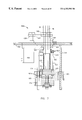
- a quartz-walled reactor 1 includes a quartz chamber 10 housing a boat 12 containing a plurality of wafers 14 which are heated by a furnace 16 having multiple zones of resistance heated elements 16 a - 16 c .
- Boat 12 typically contains between 80-150 of wafers 14 .
- a silicon nitride film is formed via chemical reaction on each of wafers 14 by injecting from tanks 17 gaseous silane or dichlorosilane and either nitrogen or ammonia into chamber 10 via an injection port 18 .
- Other films such as polysilicon, epitaxial silicon, metals, silicides, and glasses may be formed on wafers 14 in a similar fashion by injecting the appropriate reactant gases into the chamber. These reactant gases are removed from chamber 10 by an exhaust port 19 .
- Still other layers may be grown on the heated wafers such as silicon dioxide by injecting oxygen and/or water vapor into the chamber where the oxygen reacts directly with the surface of the silicon wafer to produce the SiO 2 .
- Such a hot wall CVD chamber 10 is problematic for numerous reasons.
- the reactant gases are typically injected into a first end of chamber 10 (via injection port 18 ) and removed from another end of chamber 10 (via exhaust port 19 ).
- the reactant gases are depleted as they travel through chamber 10 such that the deposition rate of the reactant vapor on those of wafers 14 proximate to injection port 18 is higher than those of wafers 14 proximate to exhaust port 19 .
- This phenomenon is known in the industry as the “gas depletion effect” and may result in unacceptable variations between films formed on the plurality of wafers 14 .
- Pre-processing time includes the time required to load the plurality of wafers 14 into boat 12 , insert boat 12 into chamber 10 , and slowly ramp up the temperature within chamber 10 from a loading/unloading temperature to a constant and uniform process temperature.
- Post-processing time includes the time required to slowly ramp the temperature down from the process temperature to the loading/unloading temperature, to remove boat 12 from chamber 10 , and to further cool boat 12 and wafers 14 therein to allow wafers 14 to be loaded into plastic wafer cassettes (not shown).
- the slow insertion rate of boat 12 into chamber 10 and removal rate of boat 12 from chamber 10 are necessary to ensure minimal temperature gradients across the surface of wafers 14 , thereby avoiding wafer warping and/or crystal slippage of wafers 14 .
- actual processing of wafers 14 may require only one-half hour, the time required for the pre- and post-processing procedures just discussed is typically 1 to 21 ⁇ 2 hours. Accordingly, this pre- and post-processing time significantly limits the throughput of chamber 10 .
- the slow temperature ramp up, the slow process of obtaining a uniform and constant temperature across the surface of wafers 14 , and the slow temperature ramp down result in chamber 10 contributing a relatively high thermal budget (the time that the wafers are above room temperature) to wafers 14 .
- the thermal budget the time that the wafers are above room temperature
- boat 12 capable of holding a large number of wafers helps to maximize throughput of chamber 10 , the simultaneous processing of so many of wafers 14 increases risk of wafer loss should something go wrong during processing. For instance, if a gas flow controller malfunctions or the vacuum pump ceases operating properly, all of wafers 14 in boat 12 may be destroyed.
- the reactor includes a vacuum chamber having two distinct sections.
- the lower section is used for the loading and unloading of the wafers and the upper section is where the temperature, pressure and the flow of gases can be precisely controlled to produce desired uniform and consistent process results.
- the reactor is connected to a central transfer vacuum chamber via a slit valve such that the wafers can be loaded into the wafer boat while under vacuum via the robotic arm of the transfer chamber.
- the wafer boat is supported by a shaft which, being movable in a vertical direction, allows wafers to be loaded/unloaded into the various slots of the wafer boat.
- the slit valve is closed and the boat containing the wafers is elevated into the upper section of the chamber.
- the wafer boat and wafers therein are heated by multiple zone radiant heaters e.g. tungsten halogen lamps arranged around the periphery of the upper section of the chamber and by additional heaters positioned about the top and bottom surfaces of the chamber. In this manner, a desired thermal profile may be obtained.
- Thermocouples inserted into a high temperature material such as graphite or silicon carbide are positioned at strategic positions within the chamber and provide temperature feedback to the controller (or computer) which, in turn, controls the various heater zones. In other embodiments, pyrometry or other means may provide this temperature feedback.
- the boat and wafers therein are rotated (typically 3 to 30 rpm).
- the process gases are injected into and exhausted from the chamber in a cross flow fashion parallel or nearly parallel to the wafers so as to result in a uniform process results.
- the flow rate of the process gases may be adjusted as function of vertical position relative to the wafer boat via independently controlled gas injection and exhaust ports. In this manner, the ability to optimize the process gas flow pattern within the chamber is realized, irrespective of the particular process gas or gases employed and irrespective of the process pressure.
- a plurality of electrically conductive shield plates surround the interior walls of the chamber. Where it is desired to perform PECVD processes and in situ plasma cleaning, RF (radio frequency) power may be applied to a first number of the plates while a second number of the plates are held at ground potential. Further, the shield plates prevent the deposition of the reactant species onto the quartz windows of the chamber and also serve to diffuse heat emitted from the heating elements.
- RF radio frequency
- the reaction chamber described below could easily be a stand alone product (without the bottom portion), where the entire boat load of wafers or flat panel displays is inserted into and removed from the reactor instead of single wafer load/unload as described below.
- the reaction chamber could be a “manual boat load/unload” reactor (or simple mechanical load/unload) instead of the robotic load/unload system described below.
- the entire machine could be flipped over such that wafer load/unload is accomplished in the upper portion and process in the lower portion.
- the preferred embodiment is described for bottom load/unload to keep the wafer transport plane (robotic arm height) closer to the floor which is more consistent with other semiconductor process equipment such as single wafer cluster tools.
- the gas injection and exhaust systems of this invention are important features. For instance, in many types of CVD furnace reactors, a quartz tube with small holes up and down its length is inserted into the main quartz tube adjacent to the wafers and the process gases are introduced via the holes in this smaller tube in an effort to overcome gas depletion effects to achieve better uniformity and higher deposition rates throughout the boat load of wafers.
- the smaller tube is in an isothermal environment with the wafers and is at the same deposition temperature, the CVD material being deposited on the wafers is also being deposited on the edges of these holes and in a relatively short period of time, this deposit will start clogging the holes and can flake off and fall onto the wafers.
- the deposition rates achievable in the reactor of this invention can be from 5 to 30 times greater than that for a typical furnace type reactor, while still maintaining desired uniformity from wafer to wafer and across each wafer.
- the tuning of the exhaust further enhances the ability to achieve maximum deposition rates while maintaining deposition uniformity on the wafers.
- the present invention provides for the heating of the exhaust plate and manifold which is desirable for many CVD processes to prevent condensation which can also lead to the generation of particles that can migrate to the wafers.
- the plasma capability of the present invention is of significance.
- the way the RF energy is coupled to opposing sets of side shield plates in conjunction with the presence of the upper and lower shield plates makes for a nearly symmetrical geometry which is important to maximize the plasma's energy uniformity.
- This design also allows for switching the RF from side to side which aids in the uniformity of material removal during in situ plasma cleaning.
- the RF input assembly is designed with dark space shielding to eliminate the creation of a plasma behind the shield plate clips which otherwise would cause hot spots in that area that would detract from the energy and uniformity of the plasma in the cleaning region of the chamber.
- the cold wall construction of the present invention a) allows for use of multiple zone radiant heating with simple and inexpensive quartz windows (the total cost of the quartz parts of the present invention is one-tenth or less the cost of replacing the quartzware of a conventional vertical furnace); b) allows for cluster tool configuration for automatic load/unload under vacuum and for sequential processing from one reactor (process A) to another (process B) and so on; c) reduces deposition on the cooled walls; d) eases attachment/removal of sub-assemblies such as the side heaters, gas injection, exhaust manifold and RF/TC seal plates; and e) permits accelerated temperature ramp down when the pressure within the chamber is increased with inert gas flow to permit greater heat conduction through the gas to the cold walls.
- the multi-zone radiant heating of the present invention provides: a) much lower thermal inertia compared to a resistively heated furnace, resulting in faster response time; b);as many as ten to twelve independent heat zones (compared to 5 to 7 for a typical vertical furnace); and c) the ability to tailor the thermal pattern within the chamber for faster temperature ramping without wafer warpage or crystal slippage.
- the wafer rotation feature of the present invention promotes better uniformity across a wafer and from wafer-to-wafer, while permitting faster deposition rates (up to 5 to 30 times faster deposition rates than a conventional furnace).
- the low thermal mass-shielded plates of the present invention have the following advantages: a) the bottom, top and side shield plates entirely surround the wafers and serve to diffuse the heat energy from the lamps for greater uniformity; b) the low thermal mass permits rapid cycling of temperature; c) the existence of these plates allows for inert gas to be injected between the plate and the quartz window to prevent the reactive process gases from penetrating and causing deposition on the window; and d) the shield plates are made of materials (graphite, silicon carbide, ceramic, etc.) that result in a very high level of adhesion of typical CVD films even during temperature cycling compared to a quartz furnace type reactor where particles of the deposited material on the quartz can easily flake off and onto wafers.
- the bottom shield plate of the present invention a) moves up and down with the wafer boat; b) can be left floating or grounded or connected to the RF energy source during plasma processing; c) provides a degree of thermal isolation between the upper process chamber and the lower load/unload chamber; d) with inert gas flow into the lower chamber, the plate serves to effectively retard the process gases from entering the lower chamber; e) the existence of the plate greatly enhances the ability to achieve a uniform gas flow pattern in the process chamber by serving as a bottom plate to the process chamber such that the top plate and the bottom shield are approximately equidistant with respect to the boat of wafers, and f) diffuses the heat from the bottom heaters.
- FIG. 1 is a cross-sectional view of a conventional hot wall CVD reactor 1 ,
- FIG. 2 is a side view of a CVD reactor in accordance with the present invention.
- FIGS. 3 and 4 are respective top and bottom views of the reactor of FIG. 2;
- FIG. 5 is a cross-sectional view of the reactor of FIG. 2 with the wafer boat in a loading/unloading position (bottom heaters not shown);
- FIG. 6 is a cross-sectional view of the reactor of FIG. 2 with the wafer boat in a processing position (bottom heaters not shown);
- FIG. 7 is an exploded cross-sectional view of the reactor of FIG. 2 illustrating a rotating mechanism in accordance with the present invention
- FIG. 8 is an exploded cross-sectional view of the reactor of FIG. 2 illustrating a first lifting mechanism in accordance with the present invention
- FIG. 9 is a cross-sectional view of the reactor of FIG. 2 illustrating a second lifting mechanism in accordance with the present invention.
- FIG. 10 is a cross-sectional view of the wafer boat in accordance with the present invention.
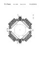
- FIG. 11 is a top cross-sectional view of the reactor of FIG. 2;
- FIG. 12 is a top cross-sectional view of a wall of the upper section of the chamber of the reactor of FIG. 2;
- FIG. 1.3 is an exploded view of FIG. 12;
- FIG. 14 is another exploded view of the wall of FIG. 12;
- FIG. 15 is a cross-sectional view of the RF input structure in accordance with the present invention.
- FIG. 16 is another cross-sectional view of the reactor's upper section
- FIG. 17 is a side view with cross-section of the RF input seal plate
- FIG. 18 is the side, top and bottom view of the side heater in accordance with the present invention.
- FIG. 19 is a cross-sectional view of the side heater
- FIG. 20 shows the three views of the lamp clip assembly
- FIGS. 21A-21C and 22 A- 22 F illustrate various positions in which heating elements may be placed in accordance with the present invention
- FIG. 23 is a cross-sectional view of a heating element positioned above the chamber within the reactor of FIG. 2;
- FIG. 24 illustrates the three zones of lamps of heating element of FIG. 23
- FIG. 25 illustrates the heating element housings positioned below the chamber within the reactor of FIG. 2;
- FIGS. 26 and 27 are cross-sectional views of one of the heating elements positioned below the chamber within the reactor of FIG. 2;
- FIGS. 28 and 29 are cross-sectional views of a thermocouple structure in accordance with the present invention.
- FIG. 30 is a cross-sectional view of gas injection systems and gas exhaust systems in accordance with the present invention.
- FIG. 31 a is a cross-sectional view of one embodiment of the gas injection system of FIG. 30;
- FIG. 31 b is a front view of the gas injection system of FIG. 31 a;
- FIG. 32 a is a cross-sectional view of another embodiment of the gas injection system of FIG. 30;
- FIG. 32 b is a front view of the gas injection system of FIG. 32 a;
- FIG. 33 a is a cross-sectional view of yet another embodiment of the gas injection system of FIG. 30;
- FIGS. 33 b and 33 c are front views of the gas injection system of FIG. 33 a illustrating various positions of injection ports;
- FIG. 34 is a cross-sectional view of still another embodiment of the gas injection system of FIG. 30;
- FIG. 35 is a side and cross-sectional view of still another embodiment of the gas injection system of FIG. 30.
- FIG. 36 is an exploded cross-sectional view of the gas injection system of FIG. 35 .
- Embodiments of the present invention are discussed below with reference to the drawing figures, where like elements are similarly labelled.
- the present invention is described below in the context of the CVD deposition of a silicon nitride film on a semiconductor wafer by way of example only.
- the teachings herein are equally applicable for the deposition or growth of other materials, for example polycrystalline silicon upon other appropriate surfaces such as flat panel displays, and to other processes performed at pressure both greater than and less than atmospheric pressure, including but not limited to thermally driven and PECVD (plasma enhanced CVD) processes.
- PECVD plasma enhanced CVD
- the teachings herein also apply to other processes requiring uniform temperatures, certain pressures and gas mixtures such as the growth of silicon dioxide, annealing, glass reflow, diffusion, etc,.
- a CVD reactor 20 includes a vacuum chamber 22 having an upper portion 22 a and a lower portion 22 b where, as explained in more detail below, lower portion 22 b is used for inserting wafers into and removing wafers from reactor 20 and upper portion 22 a is used as the processing chamber.
- Upper portion 22 a and lower portion 22 b are welded together or bolted together and vacuum sealed using an O-ring structure 24 or other conventional means.
- upper portion 22 a has four walls 100 a and four walls 100 b all of which may be cooled via recirculating water or other liquid.
- a gas injection manifold 200 and a gas exhaust manifold 300 attached to opposite walls 100 b are discussed in more detail below.
- a multiple zone heating structure 400 is attached to each of the four side walls 100 a .
- a liquid-cooled top plate 32 made of for instance aluminum is vacuum sealed via an O-ring or other means (not shown) to side walls 100 a and 100 b .
- a multiple zone heating structure 500 is positioned above top plate 32 .
- lower portion 22 b includes four side walls 34 . Attached to one of these side walls is a slit valve 36 through which a mechanical or robotic arm may insert (remove) a wafer into (from) lower portion 22 b in a well known manner.
- Slit valve 36 is vacuum sealed to its associated one of side walls 34 in a well known manner using for instance an O-ring (not shown).
- a bottom plate 38 made of for instance aluminum is attached to and vacuum sealed to each of side walls 34 using an O-ring (not shown).
- a plurality of heating structures 550 similar to heating structure 500 are attached to an exterior surface of bottom plate 38 .
- a lift and rotation mechanism 600 which is discussed in more detail below is positioned in the middle of bottom plate 38 .
- FIG. 5 which shows reactor 20 in a loading/unloading condition
- a wafer 44 is loaded into one of the plurality of slots of a wafer boat 46 by a mechanical or robotic arm through slit valve 36 (not shown in FIG. 5 ).
- Boat 46 may be constructed of any suitable high temperature material such as, for instance, quartz, silicon carbide, or graphite, depending upon desired process characteristics. Note that although shown in FIG. 5 as holding up to fifteen of wafers 44 , boat 46 may in other embodiments hold a greater or fewer number of wafers 44 .
- Boat 46 is mounted to a first end of an inner shaft 48 via a fitting 50 integrally attached to a bottom surface of boat 46 .
- Shaft 48 passes through associated openings in the middle of bottom plate 38 and between the heating structures 550 (not shown for simplicity in FIGS. 5 and 6) and into a hollow outer shaft 52 having a first end protruding upwards towards the hole of bottom plate 38 .
- a ferrofluidic or other suitable seal 54 vacuum seals outer shaft 52 to chamber 22 .
- FIG. 7 which shows a portion 600 a of a lift and rotate mechanism 600
- outer shaft 52 passes through an associated opening in an upper mount plate 602 and is secured thereto by a clamp and bearing assembly 604 .
- Outer shaft 52 is vacuum sealed to an upper bellows disk 606 via an O-ring 608 .
- An opening in the center of upper bellows disk 606 allows shaft 48 to pass into a hollow bellows 610 positioned between and welded to each of upper bellows disk 606 and a lower bellows disk 612 .
- a second end of shaft 48 is securely attached to lower bellows disk 612 .
- a lead screw 614 is positioned between upper mount plate 602 and a lower mount plate 616 .
- Lead screw 614 is affixed to upper mount plate 602 by a bearing clamp assembly (not shown) and is secured to lower mount plate 616 by a bearing assembly 618 which allows lead screw 614 to freely rotate.
- Lower bellows disk 612 is mounted onto a lift carriage 620 via a rotation disk 621 .
- Three threaded holes in lower bellows disk 612 allow leveling screws 622 (only one is shown for simplicity) to adjust the angle of shaft 48 .
- rotation disk 621 is held in place by bearing assemblies 621 a within lift carriage 620 .
- a lead nut 623 provided within lift carriage 620 engages lead screw 614 .
- the shaft of lead screw 614 passes through an associated opening in lower mount plate 616 .
- An electric motor 624 mounted to lower mount plate 616 rotates lead screw 614 via a pulley 626 attached to the shaft of lead screw 614 , a pulley 628 attached to motor 624 , and a belt 630 which engages pulleys 626 and 628 .
- One or more guide rails 632 passing through one or more associated linear bearings 634 provided within lift carriage 620 are positioned between upper mount plate 602 and lower mount plate 616 to ensure smooth vertical motion of wafer boat 46 .
- a motor 636 mounted underneath upper mount plate 602 rotates outer shaft 52 and wafers 44 via a pulley 638 coupled to motor 636 , a pulley 640 mounted about outer shaft 52 , and a belt 642 engaging pulleys 638 and 640 (FIG. 7 ).
- a slotted disk and photocell assembly 644 mounted on upper mount plate 602 stops the rotation of outer shaft 52 and wafers 44 at a predetermined “home” position to facilitate the loading and unloading of wafers 44 through slit valve 36 .
- a commercial shaft encoder could be used for the same purpose of stopping at the predetermined “home” position.
- a circular seal plate 62 having an opening formed therein through which shaft 48 passes is positioned immediately below boat 46 (FIGS. 6 and 10 ).
- Seal plate 62 is constructed from a suitable high temperature material such as for instance graphite or silicon carbide and has nested into a groove around the outer periphery of its top surface a quartz ring 64 .
- Seal plate 62 is supported by three lift rods 66 constructed from a suitable high temperature material (only one lift rod 66 is shown for simplicity). Lift rods 66 are each operatively coupled to a lift mechanism 700 (only one is shown for clarity).
- lift mechanism 700 includes a bellows 702 within which an associated one of lift rods 66 is positioned.
- Bellows 702 has a first end mounted to bottom plate 38 and vacuum sealed thereto by an O-ring 704 and has a second end mounted to a leveling disk 706 which, in turn, is mounted on a lift carriage 708 .
- Lift carriage 708 includes a linear bearing 710 which engages a guide rail 712 , thereby ensuring smooth linear motion of lift carriage 708 .
- Three leveling screws 714 are provided within leveling disk 706 to maintain lift rods 66 in a proper position.
- lifting rods 66 may be constructed using two separate rods connected together in an end-to-end fashion, where the upper one of the separate rods is quartz and the lower one of the separate rods being a high temperature material such as for instance titanium or molybdenum.
- the force acting upon the bellows 702 will be such that the bellows 702 will tend to collapse in length causing the lift rods 66 and the seal plate 62 to move upwards. Since the hole in the seal plate 62 is smaller than the diameter of the fitting 50 , the seal plate 62 and lift rods 66 can only move upwards as the boat 46 moves upwards.
- the seal plate 62 will stop its upward motion when the top surface of quartz ring 64 comes in contact with the O-ring structure 24 of the upper portion 22 a of chamber 22 . Conversely, as the boat 46 moves downward from the upper portion 22 a to the lower portion 22 b , the fitting 50 comes in contact with the seal plate 62 and thereafter the seal plate 62 will continue to move downward along with the downward motion of the boat 46 .
- a simple constant force spring mechanism pulling in the opposite or downward direction can be attached to the lift carriage 708 so that the net upward force will be maintained at lower more moderate level.
- the seal plate 62 could be raised and lowered by means of hydraulic or pneumatic actuator(s) attached to lift mechanisms 700 or an electric motor or motors could be attached to the lift mechanisms 700 for the same purpose.
- quartz ring 64 of seal plate 62 comes into intimate contact with an inner lip of O-ring structure 24 , thereby stopping seal plate 62 in the position shown in FIG. 6 .
- seal plate 62 provides an almost complete seal between upper 22 a and lower 22 b portion of chamber 22 , where portion 22 a of chamber 22 becomes a reaction chamber in which layers of suitable material may be formed on wafers 44 .
- inert gas such as argon or helium
- This inert gas flow serves to greatly minimize the amount of reactive gasses the can enter the lower portion 22 b from the upper portion 22 a thereby effectively eliminating excessive and unwanted vapor deposition upon the heated parts in lower portion 22 b .
- containment of the expensive reactive gases within the process or upper portion 22 a results in more efficient use of these gases.
- Seal plate 62 provides effective thermal isolation between reaction chamber 22 a and lower chamber portion 22 b .
- seal plate 62 also serves as a thermal diffuser for heat energy emitted from heating structure 550 and, in this manner, acts as an intermediate heat source for wafers 44 .
- seal plate 62 provides for the effective containment of the plasma within the upper portion 22 a during plasma enhanced processing such as PECVD and in situ plasma cleaning and presence of seal plate 62 in conjunction with seal plate 508 associated with the upper heating structure 500 (FIG. 18) results in a symmetrical configuration which aids in producing a uniform plasma to obtain consistent and uniform plasma processing.
- the seal plate 62 can be either held at electrical ground in the case where the lifting rods 66 are made of conductive material such as titanium or the seal plate 62 can be electrically floating if the lifting rods are made of a non-conducting material such as quartz. Alternatively, seal plate 62 may be connected to the RF source.
- one or more rotation pins 637 attached to lift carriage 620 engage associated notches 638 formed in upper bellows disk 606 (FIG. 7 ).
- the rotation pin(s) 637 transmit the rotation energy via the lower bellows disk 612 to the shaft 48 rather than via the bellows 610 thereby eliminating bellows wobble and fatigue of the bellows material (usually thin stainless steel) leading to premature failure.
- a heating structure 400 is positioned on an exterior surface of each of side walls 100 a .
- sidewalls 100 a and 100 b of process portion 22 b of chamber 22 are welded together on the inside seams thereof and have formed therein ducts 102 through which water or other suitable liquid flows for cooling purposes.
- a quartz window 104 is securely positioned within each of walls 100 a as shown in FIG. 12 by a water-cooled window clamp 106 which is fastened to side wall 100 a by bolts 108 .
- An O-ring type gasket 110 (constructed of a suitable material such as, for instance, viton, silicon rubber, or cal-rez graphite fiber) and strips 112 and gasket 111 of a similar suitable material are provided between quartz window 104 and side wall 100 a and clamp 106 to ensure that the window 104 does not come in direct contact with either the side wall 100 a or the clamp 106 to prevent the undue stress that would cause an implosion if the window 104 were in direct contact with the cooled side wall 100 a or the cooled clamp 106 when the window 104 is hot and the chamber 22 is under vacuum.
- the combination of O-ring 110 and gasket 111 also completely vacuum seals quartz window 102 to side wall 100 a . Milled channels or ducts (similar to 102 ) are formed in clamp 106 and strips of metal 117 are welded thereto to allow water or other liquid to flow through the ducts 116 for cooling the clamp 106 .
- Heating structure 400 is mounted to window clamp 106 by bolts (not shown).
- seven cylindrical tungsten halogen lamps 402 each having a piece of insulator tubing 404 made of ceramic or quartz and encasing its electrical lead wires 406 are positioned within heating structure 400 as shown in FIGS. 12 and 13. Between the lamp 402 and the heating structure 400 is positioned a shorter piece of insulating tubing 405 which has an outside diameter larger than the width of the tapered slot 407 in structure 400 through which the lead wire 406 and insulator tube 404 passes to prevent the lamp 402 from coming into contact with structure 400 .
- Heating structure 400 may, in other embodiments, be modified in order to house a greater or fewer number of lamps 402 . Those portions of the exterior surface of heating structure 400 which face the lamps 402 are polished and thereafter plated with successive layers of nickel and gold to maximize reflection.
- Strips of quartz 120 or other suitable high temperature, electrically insulating material such as ceramic are positioned within a recessed grooves formed in sidewall 100 a and which surround the entire opening in sidewall 100 a .
- a thermal shield plate 122 made of a suitable high temperature material such as, for instance, graphite or silicon carbide is secured to side wall 100 a by a plurality of retaining clamps 124 which are made from suitable high temperature material such as titanium.
- These clamps 124 are bolted to side wall 100 a via bolt 125 and both the clamps 124 and the shield plate 122 are electrically isolated from the side wall 100 a via the insulating (ceramic or other suitable material) shoulder washer 126 a , the insulating flat washer 126 b and the strips 120 .
- Shield plates 122 act as thermal plates to diffuse heat energy emitted from heating structures 400 to allow a more uniform distribution of heat energy to be provided to wafers 44 .
- the shield plates 122 preferably have low thermal mass to allow for rapid thermal cycling of the shield plates 122 .
- Inert gas such as argon is injected into the gap between the window 104 and the shield plate 122 via the gas channel in the side wall 100 a made by holes 127 a and 127 b which join together to form the gas channel (FIG. 14 ). The gas is injected into the channel via fitting 128 .
- the inert gas flows into the gap between the window 104 and the shield plate 122 and escapes out into the chamber 22 a via the small gaps between the individual quartz strips 120 (alternatively small holes are drilled in the shield plates 122 to let the gas escape in the case where the individual quartz strips are replaced by a continuous single ring of quartz).
- the flow of the inert gas retards the reactant gases within chamber 22 a from coming into contact with the quartz window 104 , thereby preventing the unwanted deposition of films on the quartz window 104 .
- all four of the shield plates 122 are electrically isolated from their associated side walls 100 a and from each other.
- two adjacent shield plates 122 are electrically connected together via the RF feedthrough structure 600 while the other two remaining shield plates are connected together via a feedthrough structure 600 on the opposite side of chamber 22 a (FIG. 16) thereby forming a symmetrical arrangement of the two sets of connected shield plates 122 to facilitate the creation of a uniform plasma within chamber 22 a .
- An electrical connection clip 601 made of suitable electrically conductive high temperature inert material such as titanium spans across the space between two adjacent side walls 100 a and makes contact with the two adjacent shield plates 122 .
- a bolt 602 passes through the center hole in clip 601 and through the clip support tube 603 which is made from suitable conductive material such as stainless steel, titanium, graphite, etc,.
- the clip support tube 603 rests against nut 604 and the bolt 602 continues through the insulating washer 605 (ceramic, etc,) and then through insulating tube 606 which is contained within a hole drilled through the RF input seal plate 607 .
- the bolt 602 then passes through the external insulating washer 608 and is threaded into the RF connector 609 (note that part of the threads along the length of the bolt 602 have been previously ground off to provide a path for trapped gases to prevent virtual leaks).
- the RF input cable or strap (not shown) coming from the RF matching network (not shown) is bolted to the connector 609 via threaded hole 610 .
- a metal enclosure 611 Surrounding the connector 609 and the RF input cable or strap is a metal enclosure 611 , usually aluminum, bolted to the RF input seal plate 607 to prevent the escape of the RF energy which could interfere with aircraft and other radio signals in the atmosphere.
- An O-ring 612 a vacuum seals the RF input connector 609 to the external insulating washer 608 which in turn is vacuum sealed to the RF input seal plate 607 via o-ring 612 b .
- the RF input seal plate 607 which is bolted to the side walls 100 a (bolts not shown) is vacuum sealed to the sidewalls 100 a via O-ring 613 .
- Surrounding the clip support tube 603 is the dark space insulating tube 614 which in turn is surrounded by the grounding enclosure 615 which is bolted to the RF input seal plate by bolts 616 .
- FIG. 17 shows an end view of the RF input seal plate 607 in which is formed the holes, o-ring grooves and bolt patterns for mounting the RF feedthrough structure in two locations 617 a and 617 b . Two locations are provided for convenience only as only one feedthrough structure 600 is required one each of the opposite sides of chamber 22 a . The unused location is vacuum sealed using a simple nut, bolt, cap and o-ring structure.
- the other holes 618 a through 618 d and their associated bolt patterns are fashioned to accept standard KF type vacuum fittings. These other holes 618 a - 618 d are used for thermocouple feedthroughs, pressure transducers, view ports and other purposes.
- Two holes, 619 a and 619 b are drilled through the RF input seal plate 607 and tapped on each end with pipe threads to accept fittings so that cooling fluid can flow through the seal plate 607 for cooling purposes. Referring to FIG.
- the use of two RF feedthrough structures 600 on opposite sides of chamber 22 a permits the use of a commercial RF switch (not shown) to switch the RF input energy from one side to the other in alternating fashion to produce more uniform removal rates of deposited material off of all four shield plates 122 during in situ plasma cleaning.
- RF energy may be provided to shield plate 508 (FIG. 23) in a similar manner. Applying RF energy also to top shield plate 508 may result in more effective in situ plasma cleaning and PECVD processes. In still other embodiments, RF energy may be provided to the lower shield plate 62 .
- Heating structures 400 may be cooled in a variety of manners.
- vertical holes 408 a - 408 f provided in structure 400 are connected together by horizontal slots 409 a - 409 e which are covered by welded plates 410 a and 410 b to form a water path throughout structure 400 , where water flow alternates upward and downward between adjacent ducts 408 .
- water provided to duct 408 a via a fitting threaded into the tapped portion 411 a flows upward in duct 408 a and downward in duct, upward in duct 408 c , and so on. Water then flows through duct 408 f and exits structure 400 via another fitting threaded into the tapped portion 411 b.
- FIGS. 21A-21C Tapered slits 407 provided within heating structure 400 allow lamps 402 to be easily positioned in various configurations within structure 400 , a few of which are illustrated in FIGS. 21A-21C which show the use of six rather than seven lamps. Slits 407 facilitate easy insertion and removal of lamps 402 and also provide a path for air to flow between, and thereby further cool lamps 402 .
- the forced air cooling is provided via a sheet metal enclosure and duct structure similar to that more fully described herein below for the top and bottom heater structures 500 and 550 .
- FIG. 20 shows the lamp clip assembly 450 (also FIG. 13 ).
- the lamp clip base 451 fabricated from, for instance, aluminum has tapered slit 453 formed therein through which a commercial spring steel anchor 452 such as supplied by Grabco, Inc. (Rolling Meadows, Ill.) is inserted.
- the base 451 and clip 452 are positioned over the tapered slit 407 and a screw(not show) is inserted into threaded hole 45 ′ which forces the legs 452 a to spread apart thus securing the clip assembly 450 to a particular position over slot 407 (see FIG. 13 ).
- the insulating tube 404 and the lamp's lead wire 406 protrude through the base 451 via hole 456 .
- a set screw or bolt 458 is threaded into tapped hole 457 to secure the insulating tube 404 .
- lamps 402 are used for each lamp 402 , one at either end. Since the anchor 452 is of spring material, the lamps 402 can be easily repositioned up and down the length of the tapered slit 407 by backing off on the screw in hole 454 and then re-tightening. In some embodiments, lamps 402 are arranged via electrical connection into two or more independently controllable zones. The flexibility in heating patterns afforded by the maneuverability of lamps 402 within structure 400 and the ability to independently control power to multiple zones of lamps 402 allows for maximum temperature uniformity across the surfaces of wafers 44 . Minimizing temperature gradients across the surfaces of wafers 44 is especially important in preventing warping and slipping during rapid temperature ramping for those processes conducted at temperatures exceeding approximately 800° C.
- the multiple zones provided by both the physical placement of the lamps and selective grouping of lamps via electrical connection allows for directing different amounts of heat to various portions of the wafer boat 46 and wafers 44 during temperature ramping. For instance, it may be desired to direct more heat towards the bottom of wafer boat 46 during temperature ramp up to produce a more uniform thermal gradient up and down the length of boat 46 to avoid warping the wafers 44 or causing crystal slippage within the wafers 44 .
- socket-type lamps 416 may be employed in place of cylindrical tungsten halogen lamps 402 , as shown in FIGS. 22A-22F.
- Lamps 416 may be positioned at various angles with respect to quartz window 104 .
- FIGS. 22A-22B shows lamps 416 positioned perpendicular to quartz window 104
- lamps 416 in the embodiment shown in FIGS. 22C-22D are positioned at various adjustable angles with respect to quartz window 104
- the embodiment shown in FIGS. 22E-22F includes lamps 416 positioned parallel to quartz window 104 .
- a water-cooled upper heating structure 500 includes nineteen apertures into which nineteen associated socket-type lamps 502 are positioned.
- lamps 502 are two-kilowatt tungsten halogen lamps.
- lamps 502 are arranged into three concentric zones 504 A, 504 B, and 504 C, where zone 504 A contains twelve lamps 502 positioned about the periphery of structure 500 , zone 504 C contains one lamp 502 at the center of structure 500 , and zone 504 B contains six lamps 502 intermediate lamps 502 in zones 504 A and 504 C. Power may be independently provided to the lamps 502 in each of zones 504 A- 504 C.
- Upper heating structure 500 is aligned with an opening in top plate 32 into which a quartz window 506 is provided, as shown in FIG. 23.
- a shield plate 508 is mounted against a quartz ring 510 by clips 512 .
- Shield plate 508 which is preferably made of a suitable high temperature material and has low thermal mass, diffuses heat energy generated by lamps 502 .
- Clips 512 should be constructed from a suitable high temperature material.
- An air hose (not shown) is connected to an air inlet 514 and forces air flow within inner walls 516 and then into the interior of structure 500 to cool lamps 502 .
- Inner walls 516 is bolted to a top plate 520 which, in turn, is secured to outer wall 518 by a metal ring 522 .
- the air having cooled lamps 502 and the electrical wiring associated therewith, as well as quartz window 506 , exits structure 500 through holes 533 and then exits via a duct 524 .
- a water-cooled clamp ring 526 secures heating structure 500 to top plate 32 of reactor 20 and also serves to secure quartz window 506 in place.
- O-rings 528 vacuum seal quartz window 506 to top plate 32 .
- a cushion or gasket 534 made from suitable material such as graphite or silicon rubber is positioned around the bottom periphery of window 506 to prevent the hot window from coming into direct contact with the cooled top plate 32 .
- Inert gas is introduced into the spacing intermediate quartz window 506 and shield plate 508 via an inert gas fitting 530 and associated gas duct 532 formed within top plate 32 .
- lower heating structures 550 are similar in construction to upper heating structure 500 .
- four such lower heating structures 550 are attached to bottom plate 38 with each having lamp casings 560 containing three lamps 552 .
- the lower heating structures 550 are arranged about the lifting mechanisms 700 with the ferrofluidic seal 54 in the middle.
- lamps 552 are two-kilowatt tungsten halogen lamps. Note that in other embodiments a different number of lower heating structures 550 may be provided, and that lamp casings 560 may contain a greater or fewer number of lamps 552 .
- Each of water-cooled lamp casings 560 includes a sheet-metal cover 562 (FIG. 26 ). Attached to an inner circumference of cover 562 is a bottom plate 564 . An air duct 585 is provided to allow forced air to circulate around the lamp sockets and wiring, the lamps 552 and the quartz window 570 for cooling purposes. The forced air exits via holes 586 . Water inlets 566 are provided in casing 560 to allow water or other liquid to be pumped therein for further cooling of the casing 560 . Casings 560 are secured to bottom plate 38 by a water-cooled clamp ring 568 which also secures a quartz window 570 in position. O-rings 572 vacuum seal quartz window 570 to bottom plate 38 .
- a gasket 574 ensures that the quartz window does not come into direct contact with the water cooled bottom plate 38 .
- a quartz ring 576 which nests into a recess in bottom plate 38 supports a shield plate 578 and serves to minimize heat loss from the shield plate 578 to the bottom plate 38 .
- High temperature clips 580 made from metal or other suitable material secure shield plate 578 in position just above quartz window 570 .
- An inert gas fitting 582 and associated duct 584 nearly identical in construction to respective inert gas fitting 530 and duct 532 of structure 500 are formed in bottom plate 38 .
- one or more of casings 560 may be mounted to bottom plate 38 at some predetermined angle, as illustrated for instance in FIG. 27, to provide further flexibility in directing the heat from the lower heating structures 550 towards different areas within the reactor 20 .
- casing 560 contains one high-powered lamp 522 a , as opposed to three of lamps 552 .
- the shapes of respective ring clamp 568 and quartz ring 576 will differ depending upon the particular angle at which their associated casing 560 is attached to bottom plate 38 .
- the flexibility in the positioning of casings 560 allows for a more uniform distribution of heat to be provided to wafers 44 being processed in accordance with the present invention.
- Temperature readings of wafers 44 obtained using suitable temperature sensoring devices are provided as feedback to one or more temperature controllers which, in response thereto, adjust the intensity of one or more associated zones of lamps 402 , 502 , and 552 within respective heating structures 400 , 500 , and 550 in a well known manner.
- Suitable temperature controllers are available from Eurotherm, Inc of Reston, Va.
- feedback temperature readings may be provided to a computer, where the manipulation of power provided to the lamps, and thus the temperature of wafers 44 within reactor 20 , is implemented in a well known manner by PID control software operating in association with the computer.
- thermocouple 136 employs as the temperature sensing device a plurality of thermocouples 136 .
- a thermocouple 136 enters reactor 20 through a vacuum feedthrough 138 attached to side wall 34 and continues into the reaction chamber through a hole 139 and associated opening in O-ring structure 24 .
- thermocouple 136 is a metal sheathed type encapsulated by concentric layers of a quartz or ceramic tubing 142 and a graphite, silicon carbide, or other high temperature tubing 144 . The end of the metal sheathed thermocouple is completely encapsulated by tubing layer 142 to prevent a glow discharge within reaction chamber 22 a from contacting the thermocouple 136 .
- thermocouples 136 may be encased in only one layer of tubing made of quartz, ceramic, graphite, silicon carbide or other suitable material.
- the sheathed thermocouples 136 may not be encased at all, however, in some cases for particular thermocouple 136 locations, an unencased thermocouple's thermal response time may be too fast for properly controlling the temperature via the PID controller.
- the thermocouples 136 may enter the reaction chamber 22 a via a feedthrough attached to a hole or holes in seal plate 607 that are not being used for the RF feedthrough structure 600 .
- thermocouples 136 may be employed at various positions within reactor 20 in order to increase the accuracy with which wafers 44 are maintained at a constant and uniform temperature and the accuracy with which wafers 44 are ramped up to and down from such constant and uniform temperature to avoid warpage or crystal slippage of wafers 44 .
- thermocouples 136 may be positioned within shield plates 122 , 508 and 578 .
- temperature sensing may be accomplished using pyrometry.
- one or more pyrometers are mounted in suitable locations about reactor 20 and provide feedback indicative of the temperature of wafers 44 to one or more temperature controllers which, as discussed above, adjust the intensity of one or more associated zones of lamps 402 , 502 , and 552 within respective heating structures 400 , 500 , and 550 .
- process gases to be used in depositing layers on wafers 44 are provided via ducts 202 to a mixing chamber 204 which, along with a plurality of gas flow control devices 206 and a water-cooled injection plate 210 , is included within gas injection manifold 200 .
- Injection plate 204 is vacuum sealed to one of side walls 100 b via an O-ring (not shown).
- the process gases are provided to ports 208 formed in injection plate 210 via associated flow rate control devices 206 which collectively allow for precise control over the amount of process gas flow provided into reaction chamber 22 a.
- Exhaust manifold 300 includes an exhaust plate 302 having plurality of exhaust ports 304 , an exhaust plenum 306 , a control throttle valve 308 , and gate valve 310 and is vacuum sealed to the other of walls 100 b via an O-ring (not shown). Process gases are removed from reaction chamber 22 a through the plurality of ports 304 and are provided to exhaust plenum 306 via a plurality of associated exhaust flow control devices 312 which, in some embodiments, are similar to flow rate control devices 206 . Process gases then flow through control throttle valve 308 and gate valve 310 to an external vacuum pump system (not shown). Exhaust plate 302 may be either cooled or heated via recirculating liquid or other means, depending upon the particular process employed.
- Flow rate control devices 206 and exhaust flow control devices 312 may be independently adjusted to allow for optimum process gas flow pattern within the reaction chamber 22 a.
- injection plate 208 includes a single slot 212 through which the process gases enter the reaction chamber 22 a , as shown in FIGS. 31 a and 31 b .
- a shutter plate 214 may be affixed to injection plate 208 at any desired angles to further control the amount of gas provided to reaction chamber 22 a , as shown in FIGS. 32 a and 32 b .
- the embodiment shown in FIGS. 31 a - 31 b and the embodiment shown in FIGS. 32 a - 32 b include a plenum 216 attached and sealed to injection plate 208 via an O-ring 218 .
- a plate similar to shutter plate 212 may be affixed to exhaust plate 302 to further control the flow of exhaust gas.
- shutter plate 214 may be replaced with a plate 220 having a plurality of small vias through which process gases provided to plenum 216 may flow into reaction chamber 22 a , as shown in FIG. 33 a .
- the plurality of vias formed in plate 220 may be arranged in any suitable manner, two examples of which are provided in respective FIGS. 33 b and 33 c .
- Plate 220 may also be liquid cooled. Note that a plate similar to plate 220 may be provided within exhaust manifold 300 to facilitate removal of process gases from reaction chamber 22 a.
- injection plate 208 may include one or more vertical gas supply shafts 222 into which are coupled a plurality of horizontal gas ducts 224 , as shown in FIG. 34 .
- Sintered metal disks 226 may be press fitted into counterbores at an end of ducts 224 to produce a more laminar gas flow and to reduce the entry of undesirable particles into reaction chamber 22 a .
- Each of ducts 224 has provided therein a gas flow adjustment screw 228 which, by varying the cross-sectional area of ducts 224 through which process gas flows, controls the flow of reactant gas to reaction chamber 22 a .
- Screws 228 are sealed to associated ducts 224 via O-rings (not shown).
- a similar duct structure may be employed to control the removal of process gases from reaction chamber 22 a via exhaust manifold 300 .
- the process gases separately enter the reaction chamber 22 a and thus are mixed therein.
- the injection plate 208 has formed therein on the side facing the interior of chamber 22 a a plurality (two shown) of slots 231 a and 231 b .
- a thinner plate 234 having a plurality of holes 236 which line up over the slots 231 a and 231 b is bolted to injection plate 208 .
- the size, number and spacing of the holes in plate 234 may be varied throughout its length in order to produce the desired gas flow pattern to achieve uniform and consistent depositions onto all of the wafers 44 in wafer boat 46 .
- inert gas is injected into lower chamber portion 22 b via a gas inlet 68 to retard process gases escaping process chamber 22 a and entering lower chamber portion 22 b (FIG. 6 ).
- Electric motor 636 is activated and rotates shaft 48 and wafers 44 at a desired rate such as, for instance, between approximately 3 and 30 rpms.
- Power provided to the independent zones of heaters 400 , 500 , and 550 is adjusted to bring the temperature of reaction chamber 22 a to a desired processing temperature, as described above. Once the temperature of wafers 44 has stabilized in a uniform manner at the desired process temperature, reactant gases are injected into reaction chamber process portion 22 a of chamber 20 via gas injection manifold 200 and are exhausted therefrom via exhaust manifold 300 , as discussed above.
Abstract
Description
Claims (20)
Priority Applications (15)
| Application Number | Priority Date | Filing Date | Title |
|---|---|---|---|
| US08/909,461 US6352593B1 (en) | 1997-08-11 | 1997-08-11 | Mini-batch process chamber |
| KR1020007001425A KR100625890B1 (en) | 1997-08-11 | 1998-08-10 | An apparatus for processing a plurality of semiconductor wafers |
| EP98940824A EP1027473A4 (en) | 1997-08-11 | 1998-08-10 | Mini-batch process chamber |
| JP2000506395A JP2001512789A (en) | 1997-08-11 | 1998-08-10 | Mini-batch process chamber |
| PCT/US1998/016519 WO1999007915A1 (en) | 1997-08-11 | 1998-08-10 | Mini-batch process chamber |
| US09/228,840 US6321680B2 (en) | 1997-08-11 | 1999-01-12 | Vertical plasma enhanced process apparatus and method |
| US09/229,975 US6352594B2 (en) | 1997-08-11 | 1999-01-14 | Method and apparatus for improved chemical vapor deposition processes using tunable temperature controlled gas injectors |
| US09/396,588 US6287635B1 (en) | 1997-08-11 | 1999-09-15 | High rate silicon deposition method at low pressures |
| US09/396,586 US6235652B1 (en) | 1997-08-11 | 1999-09-15 | High rate silicon dioxide deposition at low pressures |
| US09/396,590 US6506691B2 (en) | 1997-08-11 | 1999-09-15 | High rate silicon nitride deposition method at low pressures |
| US09/954,705 US6780464B2 (en) | 1997-08-11 | 2001-09-10 | Thermal gradient enhanced CVD deposition at low pressure |
| US10/216,079 US20030049372A1 (en) | 1997-08-11 | 2002-08-09 | High rate deposition at low pressures in a small batch reactor |
| US10/342,151 US7393561B2 (en) | 1997-08-11 | 2003-01-13 | Method and apparatus for layer by layer deposition of thin films |
| US10/918,498 US20050013937A1 (en) | 1997-08-11 | 2004-08-13 | Thermal gradient enhanced CVD deposition at low pressure |
| US10/966,245 US20050188923A1 (en) | 1997-08-11 | 2004-10-15 | Substrate carrier for parallel wafer processing reactor |
Applications Claiming Priority (1)
| Application Number | Priority Date | Filing Date | Title |
|---|---|---|---|
| US08/909,461 US6352593B1 (en) | 1997-08-11 | 1997-08-11 | Mini-batch process chamber |
Related Parent Applications (3)
| Application Number | Title | Priority Date | Filing Date |
|---|---|---|---|
| US09/228,835 Continuation-In-Part US6167837B1 (en) | 1997-08-11 | 1999-01-12 | Apparatus and method for plasma enhanced chemical vapor deposition (PECVD) in a single wafer reactor |
| US09/228,840 Continuation-In-Part US6321680B2 (en) | 1997-08-11 | 1999-01-12 | Vertical plasma enhanced process apparatus and method |
| US09/396,590 Continuation-In-Part US6506691B2 (en) | 1997-08-11 | 1999-09-15 | High rate silicon nitride deposition method at low pressures |
Related Child Applications (6)
| Application Number | Title | Priority Date | Filing Date |
|---|---|---|---|
| US09/228,835 Continuation-In-Part US6167837B1 (en) | 1997-08-11 | 1999-01-12 | Apparatus and method for plasma enhanced chemical vapor deposition (PECVD) in a single wafer reactor |
| US09/228,840 Continuation-In-Part US6321680B2 (en) | 1997-08-11 | 1999-01-12 | Vertical plasma enhanced process apparatus and method |
| US09/229,975 Continuation-In-Part US6352594B2 (en) | 1997-08-11 | 1999-01-14 | Method and apparatus for improved chemical vapor deposition processes using tunable temperature controlled gas injectors |
| US09/396,590 Division US6506691B2 (en) | 1997-08-11 | 1999-09-15 | High rate silicon nitride deposition method at low pressures |
| US09/954,705 Continuation-In-Part US6780464B2 (en) | 1997-08-11 | 2001-09-10 | Thermal gradient enhanced CVD deposition at low pressure |
| US10/216,079 Continuation-In-Part US20030049372A1 (en) | 1997-08-11 | 2002-08-09 | High rate deposition at low pressures in a small batch reactor |
Publications (1)
| Publication Number | Publication Date |
|---|---|
| US6352593B1 true US6352593B1 (en) | 2002-03-05 |
Family
ID=25427265
Family Applications (2)
| Application Number | Title | Priority Date | Filing Date |
|---|---|---|---|
| US08/909,461 Expired - Lifetime US6352593B1 (en) | 1997-08-11 | 1997-08-11 | Mini-batch process chamber |
| US09/396,590 Expired - Fee Related US6506691B2 (en) | 1997-08-11 | 1999-09-15 | High rate silicon nitride deposition method at low pressures |
Family Applications After (1)
| Application Number | Title | Priority Date | Filing Date |
|---|---|---|---|
| US09/396,590 Expired - Fee Related US6506691B2 (en) | 1997-08-11 | 1999-09-15 | High rate silicon nitride deposition method at low pressures |
Country Status (5)
| Country | Link |
|---|---|
| US (2) | US6352593B1 (en) |
| EP (1) | EP1027473A4 (en) |
| JP (1) | JP2001512789A (en) |
| KR (1) | KR100625890B1 (en) |
| WO (1) | WO1999007915A1 (en) |
Cited By (60)
| Publication number | Priority date | Publication date | Assignee | Title |
|---|---|---|---|---|
| US6499427B1 (en) * | 1997-05-09 | 2002-12-31 | Semiconductor Energy Laboratory Co., Ltd. | Plasma CVD apparatus |
| US20030060030A1 (en) * | 2001-09-25 | 2003-03-27 | Kwang-Myung Lee | Method for processing a wafer and apparatus for performing the same |
| US6573198B2 (en) * | 2001-10-10 | 2003-06-03 | Asm International N.V. | Earthquake protection for semiconductor processing equipment |
| US6656284B1 (en) * | 2002-06-28 | 2003-12-02 | Jusung Engineering Co., Ltd. | Semiconductor device manufacturing apparatus having rotatable gas injector and thin film deposition method using the same |
| US20040129213A1 (en) * | 2003-01-07 | 2004-07-08 | Shreter Yury Georgievich | Chemical vapor deposition reactor |
| US20040149211A1 (en) * | 2002-07-18 | 2004-08-05 | Jae-Young Ahn | Systems including heated shower heads for thin film deposition and related methods |
| US20040208533A1 (en) * | 2002-01-16 | 2004-10-21 | Sacha Corbeil | Synchronization of pulse and data sources |
| US20050013937A1 (en) * | 1997-08-11 | 2005-01-20 | Cook Robert C. | Thermal gradient enhanced CVD deposition at low pressure |
| US20050150455A1 (en) * | 1999-08-13 | 2005-07-14 | Tokyo Electron Limited | Processing apparatus and processing method |
| US20050188923A1 (en) * | 1997-08-11 | 2005-09-01 | Cook Robert C. | Substrate carrier for parallel wafer processing reactor |
| US6972071B1 (en) * | 1999-07-13 | 2005-12-06 | Nordson Corporation | High-speed symmetrical plasma treatment system |
| US20060060920A1 (en) * | 2004-09-17 | 2006-03-23 | Applied Materials, Inc. | Poly-silicon-germanium gate stack and method for forming the same |
| US20060084283A1 (en) * | 2004-10-20 | 2006-04-20 | Paranjpe Ajit P | Low temperature sin deposition methods |
| US20060128139A1 (en) * | 2004-12-14 | 2006-06-15 | Applied Materials, Inc. | Process sequence for doped silicon fill of deep trenches |
| US20070049053A1 (en) * | 2005-08-26 | 2007-03-01 | Applied Materials, Inc. | Pretreatment processes within a batch ALD reactor |
| CN1303647C (en) * | 2003-09-30 | 2007-03-07 | 佳能株式会社 | Heating method, heating apparatus, and production method of image display apparatus |
| US20070061487A1 (en) * | 2005-02-01 | 2007-03-15 | Moore James F | Systems and methods for use of structured and unstructured distributed data |
| US20070059128A1 (en) * | 2005-08-31 | 2007-03-15 | Applied Materials, Inc. | Batch deposition tool and compressed boat |
| US20070056950A1 (en) * | 2005-09-09 | 2007-03-15 | Applied Materials, Inc. | Removable heater |
| US20070065578A1 (en) * | 2005-09-21 | 2007-03-22 | Applied Materials, Inc. | Treatment processes for a batch ALD reactor |
| US20070084408A1 (en) * | 2005-10-13 | 2007-04-19 | Applied Materials, Inc. | Batch processing chamber with diffuser plate and injector assembly |
| US20070084406A1 (en) * | 2005-10-13 | 2007-04-19 | Joseph Yudovsky | Reaction chamber with opposing pockets for gas injection and exhaust |
| US20070243317A1 (en) * | 2002-07-15 | 2007-10-18 | Du Bois Dale R | Thermal Processing System and Configurable Vertical Chamber |
| US20080036155A1 (en) * | 2004-12-21 | 2008-02-14 | Rigaku Corporation | Ferrofluid Seal Unit Used on Vertical Thermal Processing Furnace System for Semiconductor Wafer |
| US20080219824A1 (en) * | 2007-03-05 | 2008-09-11 | Applied Materials, Inc. | Multiple substrate transfer robot |
| US20080220150A1 (en) * | 2007-03-05 | 2008-09-11 | Applied Materials, Inc. | Microbatch deposition chamber with radiant heating |
| US20090004405A1 (en) * | 2007-06-29 | 2009-01-01 | Applied Materials, Inc. | Thermal Batch Reactor with Removable Susceptors |
| US7685885B2 (en) | 2007-12-10 | 2010-03-30 | Teradyne, Inc. | Manipulator constant force spring counterbalance |
| US20100086004A1 (en) * | 2008-10-07 | 2010-04-08 | Dow Global Technologies Inc. | Heating Chamber and Screening Methods |
| US20100218725A1 (en) * | 2009-02-27 | 2010-09-02 | Mrl Industries, Inc. | Apparatus for manufacture of solar cells |
| US20110124201A1 (en) * | 2007-07-30 | 2011-05-26 | Micron Technology, Inc. | Chemical vaporizer for material deposition systems and associated methods |
| US20110143551A1 (en) * | 2008-04-28 | 2011-06-16 | Christophe Borean | Device and process for chemical vapor phase treatment |
| US20110180097A1 (en) * | 2010-01-27 | 2011-07-28 | Axcelis Technologies, Inc. | Thermal isolation assemblies for wafer transport apparatus and methods of use thereof |
| US20110259432A1 (en) * | 2006-11-21 | 2011-10-27 | David Keith Carlson | Independent radiant gas preheating for precursor disassociation control and gas reaction kinetics in low temperature cvd systems |
| US20110293829A1 (en) * | 2005-03-18 | 2011-12-01 | Hiroshi Nagata | Coating method and apparatus, a permanent magnet, and manufacturing method thereof |
| US20110305544A1 (en) * | 2005-08-05 | 2011-12-15 | Aihua Chen | Method and apparatus for processing semiconductor work pieces |
| US20120067286A1 (en) * | 2009-03-16 | 2012-03-22 | Alta Devices, Inc. | Vapor deposition reactor system and methods thereof |
| JP4912463B2 (en) * | 2006-07-12 | 2012-04-11 | アプライド マテリアルズ インコーポレイテッド | Multi-zone heater for furnace |
| CN102560433A (en) * | 2005-06-08 | 2012-07-11 | 应用材料公司 | Rotating substrate support and methods of use |
| US20130052348A1 (en) * | 2007-11-27 | 2013-02-28 | Asm Genitech Korea Ltd. | Atomic layer deposition apparatus |
| WO2013072820A1 (en) * | 2011-11-14 | 2013-05-23 | Lam Research Ag | Device and method for processing wafer-shaped articles |
| US20130284096A1 (en) * | 2012-04-25 | 2013-10-31 | Ashish Goel | Cooled reflective adapter plate for a deposition chamber |
| US20140134332A1 (en) * | 2012-11-15 | 2014-05-15 | Spansion Llc | Distribution of Gas Over A Semiconductor Water in Batch Processing |
| CN103959440A (en) * | 2011-11-17 | 2014-07-30 | 株式会社Eugene科技 | Apparatus comprising heat-blocking plate for treating substrate |
| US8815635B2 (en) | 2010-11-05 | 2014-08-26 | Semiconductor Energy Laboratory Co., Ltd. | Manufacturing method of photoelectric conversion device |
| CN104025259A (en) * | 2012-01-04 | 2014-09-03 | 株式会社Eugene科技 | Substrate treatment device including treatment unit |
| US8895116B2 (en) | 2010-11-04 | 2014-11-25 | Semiconductor Energy Laboratory Co., Ltd. | Manufacturing method of crystalline semiconductor film and manufacturing method of semiconductor device |
| US20140345801A1 (en) * | 2011-11-17 | 2014-11-27 | Eugene Technology Co., Ltd. | Apparatus for processing substrate for supplying reaction gas having phase difference |
| CN104205299A (en) * | 2012-04-26 | 2014-12-10 | 应用材料公司 | Methods and apparatus for controlling substrate uniformity |
| US20150013909A1 (en) * | 2011-11-17 | 2015-01-15 | Eugene Technology Co., Ltd. | Substrate processing apparatus including auxiliary gas supply port |
| CN104620354A (en) * | 2012-06-27 | 2015-05-13 | 新意技术股份有限公司 | Substrate heating device and process chamber |
| US20150140835A1 (en) * | 2012-07-30 | 2015-05-21 | Hitachi Kokusai Electric Inc. | Substrate processing apparatus, method for manufacturing semiconductor device, and recording medium |
| US9368380B2 (en) | 2013-04-08 | 2016-06-14 | Eugene Technology Co., Ltd. | Substrate processing device with connection space |
| EP3211663A1 (en) * | 2016-02-29 | 2017-08-30 | Tempress IP B.V. | Horizontal furnace system and method for handling wafer boats, and wafer boat |
| WO2019099125A1 (en) * | 2017-11-16 | 2019-05-23 | Applied Materials, Inc. | High pressure steam anneal processing apparatus |
| US10364498B2 (en) * | 2014-03-31 | 2019-07-30 | Kabushiki Kaisha Toshiba | Gas supply pipe, and gas treatment equipment |
| CN111755564A (en) * | 2018-04-28 | 2020-10-09 | 深圳市拉普拉斯能源技术有限公司 | Production process of solar cell surface passivation film |
| CN111883471A (en) * | 2020-08-24 | 2020-11-03 | 台州市老林装饰有限公司 | Wafer discharging box height adjusting type placing table seat mechanism |
| EP4174919A1 (en) * | 2021-11-02 | 2023-05-03 | ASM IP Holding B.V. | Substrate processing apparatus |
| US11728142B2 (en) * | 2019-08-29 | 2023-08-15 | Samsung Electronics Co., Ltd. | Apparatus for conducting plasma surface treatment, board treatment system having the same |
Families Citing this family (15)
| Publication number | Priority date | Publication date | Assignee | Title |
|---|---|---|---|---|
| GB2335929B (en) * | 1997-06-24 | 2000-03-29 | Nec Corp | Apparatus for depositing a thin film on a substrate |
| DE69937255T2 (en) * | 1998-11-20 | 2008-07-03 | Steag RTP Systems, Inc., San Jose | QUICK-HEATING AND COOLING DEVICE FOR SEMICONDUCTOR WAFER |
| JP4329403B2 (en) * | 2003-05-19 | 2009-09-09 | 東京エレクトロン株式会社 | Plasma processing equipment |
| US7220687B2 (en) * | 2004-06-25 | 2007-05-22 | Applied Materials, Inc. | Method to improve water-barrier performance by changing film surface morphology |
| WO2006007313A2 (en) | 2004-06-25 | 2006-01-19 | Applied Materials, Inc. | Improving water-barrier performance of an encapsulating film |
| US7214600B2 (en) * | 2004-06-25 | 2007-05-08 | Applied Materials, Inc. | Method to improve transmittance of an encapsulating film |
| US7427571B2 (en) * | 2004-10-15 | 2008-09-23 | Asm International, N.V. | Reactor design for reduced particulate generation |
| KR100698404B1 (en) | 2005-06-24 | 2007-03-23 | 주식회사 유진테크 | CVD apparatus which has rotation type Heater and the control method |
| US7418982B2 (en) * | 2006-05-17 | 2008-09-02 | Taiwan Semiconductor Manufacturing Co., Ltd. | Substrate carrier and facility interface and apparatus including same |
| JP5293220B2 (en) * | 2009-01-26 | 2013-09-18 | 富士電機株式会社 | Deposition equipment |
| JP5975192B1 (en) * | 2015-01-21 | 2016-08-23 | 住友電気工業株式会社 | Silicon carbide single crystal growth apparatus and method for producing silicon carbide single crystal |
| KR101720620B1 (en) * | 2015-04-21 | 2017-03-28 | 주식회사 유진테크 | Substrate Processing Apparatus and Method of Cleaning Chamber |
| US11670490B2 (en) | 2017-09-29 | 2023-06-06 | Taiwan Semiconductor Manufacturing Co., Ltd. | Integrated circuit fabrication system with adjustable gas injector |
| US10998205B2 (en) * | 2018-09-14 | 2021-05-04 | Kokusai Electric Corporation | Substrate processing apparatus and manufacturing method of semiconductor device |
| JP7300898B2 (en) * | 2019-06-11 | 2023-06-30 | 東京エレクトロン株式会社 | Substrate processing method and substrate processing apparatus |
Citations (24)
| Publication number | Priority date | Publication date | Assignee | Title |
|---|---|---|---|---|
| US4105810A (en) | 1975-06-06 | 1978-08-08 | Hitachi, Ltd. | Chemical vapor deposition methods of depositing zinc boro-silicated glasses |
| US4178877A (en) * | 1977-03-11 | 1979-12-18 | Fujitsu Limited | Apparatus for plasma treatment of semiconductor materials |
| JPS61197638A (en) | 1985-02-28 | 1986-09-01 | Sumitomo Bakelite Co Ltd | Method and apparatus for carrying out plasma treatment |
| US4693777A (en) | 1984-11-30 | 1987-09-15 | Kabushiki Kaisha Toshiba | Apparatus for producing semiconductor devices |
| US4728389A (en) * | 1985-05-20 | 1988-03-01 | Applied Materials, Inc. | Particulate-free epitaxial process |
| US4745088A (en) * | 1985-02-20 | 1988-05-17 | Hitachi, Ltd. | Vapor phase growth on semiconductor wafers |
| US4858557A (en) * | 1984-07-19 | 1989-08-22 | L.P.E. Spa | Epitaxial reactors |
| US4870245A (en) * | 1985-04-01 | 1989-09-26 | Motorola, Inc. | Plasma enhanced thermal treatment apparatus |
| US4951601A (en) | 1986-12-19 | 1990-08-28 | Applied Materials, Inc. | Multi-chamber integrated process system |
| US4969416A (en) | 1986-07-03 | 1990-11-13 | Emcore, Inc. | Gas treatment apparatus and method |
| JPH0311546A (en) | 1989-06-09 | 1991-01-18 | Jeol Ltd | Mass analyzer for high frequency inductive coupling plasma |
| US5067437A (en) * | 1988-03-28 | 1991-11-26 | Kabushiki Kaisha Toshiba | Apparatus for coating of silicon semiconductor surface |
| US5198071A (en) * | 1991-11-25 | 1993-03-30 | Applied Materials, Inc. | Process for inhibiting slip and microcracking while forming epitaxial layer on semiconductor wafer |
| US5203956A (en) | 1990-01-08 | 1993-04-20 | Lsi Logic Corporation | Method for performing in-situ etch of a CVD chamber |
| US5272417A (en) | 1989-05-12 | 1993-12-21 | Tadahiro Ohmi | Device for plasma process |
| US5291030A (en) | 1992-06-04 | 1994-03-01 | Torrex Equipment Corporation | Optoelectronic detector for chemical reactions |
| US5383984A (en) * | 1992-06-17 | 1995-01-24 | Tokyo Electron Limited | Plasma processing apparatus etching tunnel-type |
| US5458724A (en) | 1989-03-08 | 1995-10-17 | Fsi International, Inc. | Etch chamber with gas dispersing membrane |
| US5493987A (en) | 1994-05-16 | 1996-02-27 | Ag Associates, Inc. | Chemical vapor deposition reactor and method |
| JPH08138620A (en) | 1994-11-07 | 1996-05-31 | Shimadzu Corp | Mass spectrometer |
| US5551985A (en) | 1995-08-18 | 1996-09-03 | Torrex Equipment Corporation | Method and apparatus for cold wall chemical vapor deposition |
| US5626678A (en) | 1994-01-25 | 1997-05-06 | Applied Materials, Inc. | Non-conductive alignment member for uniform plasma processing of substrates |
| US5663087A (en) | 1993-09-21 | 1997-09-02 | Nec Corporation | Method for forming silicon nitride film having low leakage current and high break down voltage |
| US5844195A (en) | 1996-11-18 | 1998-12-01 | Applied Materials, Inc. | Remote plasma source |
Family Cites Families (13)
| Publication number | Priority date | Publication date | Assignee | Title |
|---|---|---|---|---|
| DE3429899A1 (en) * | 1983-08-16 | 1985-03-07 | Canon K.K., Tokio/Tokyo | METHOD FOR FORMING A DEPOSITION FILM |
| US4784874A (en) * | 1985-02-20 | 1988-11-15 | Canon Kabushiki Kaisha | Process for forming deposited film |
| JPH0647727B2 (en) * | 1985-12-24 | 1994-06-22 | キヤノン株式会社 | Deposited film formation method |
| US5391232A (en) * | 1985-12-26 | 1995-02-21 | Canon Kabushiki Kaisha | Device for forming a deposited film |
| US5427824A (en) * | 1986-09-09 | 1995-06-27 | Semiconductor Energy Laboratory Co., Ltd. | CVD apparatus |
| JPH01125821A (en) * | 1987-11-10 | 1989-05-18 | Matsushita Electric Ind Co Ltd | Vapor growth device |
| JP2502661B2 (en) * | 1988-03-04 | 1996-05-29 | 松下電器産業株式会社 | Vapor phase growth equipment |
| US5108792A (en) | 1990-03-09 | 1992-04-28 | Applied Materials, Inc. | Double-dome reactor for semiconductor processing |
| JP2875945B2 (en) | 1993-01-28 | 1999-03-31 | アプライド マテリアルズ インコーポレイテッド | Method of depositing silicon nitride thin film on large area glass substrate at high deposition rate by CVD |
| DE69421463T2 (en) | 1993-07-30 | 2000-02-10 | Applied Materials Inc | Deposit of silicon nitride |
| US5650197A (en) * | 1994-03-11 | 1997-07-22 | Jet Process Corporation | Jet vapor deposition of organic molecule guest-inorganic host thin films |
| JPH08167605A (en) | 1994-12-15 | 1996-06-25 | Mitsubishi Electric Corp | Method of manufacturing silicon nitride film |
| US6167837B1 (en) * | 1998-01-15 | 2001-01-02 | Torrex Equipment Corp. | Apparatus and method for plasma enhanced chemical vapor deposition (PECVD) in a single wafer reactor |
-
1997
- 1997-08-11 US US08/909,461 patent/US6352593B1/en not_active Expired - Lifetime
-
1998
- 1998-08-10 WO PCT/US1998/016519 patent/WO1999007915A1/en active IP Right Grant
- 1998-08-10 JP JP2000506395A patent/JP2001512789A/en active Pending
- 1998-08-10 KR KR1020007001425A patent/KR100625890B1/en not_active IP Right Cessation
- 1998-08-10 EP EP98940824A patent/EP1027473A4/en not_active Withdrawn
-
1999
- 1999-09-15 US US09/396,590 patent/US6506691B2/en not_active Expired - Fee Related
Patent Citations (24)
| Publication number | Priority date | Publication date | Assignee | Title |
|---|---|---|---|---|
| US4105810A (en) | 1975-06-06 | 1978-08-08 | Hitachi, Ltd. | Chemical vapor deposition methods of depositing zinc boro-silicated glasses |
| US4178877A (en) * | 1977-03-11 | 1979-12-18 | Fujitsu Limited | Apparatus for plasma treatment of semiconductor materials |
| US4858557A (en) * | 1984-07-19 | 1989-08-22 | L.P.E. Spa | Epitaxial reactors |
| US4693777A (en) | 1984-11-30 | 1987-09-15 | Kabushiki Kaisha Toshiba | Apparatus for producing semiconductor devices |
| US4745088A (en) * | 1985-02-20 | 1988-05-17 | Hitachi, Ltd. | Vapor phase growth on semiconductor wafers |
| JPS61197638A (en) | 1985-02-28 | 1986-09-01 | Sumitomo Bakelite Co Ltd | Method and apparatus for carrying out plasma treatment |
| US4870245A (en) * | 1985-04-01 | 1989-09-26 | Motorola, Inc. | Plasma enhanced thermal treatment apparatus |
| US4728389A (en) * | 1985-05-20 | 1988-03-01 | Applied Materials, Inc. | Particulate-free epitaxial process |
| US4969416A (en) | 1986-07-03 | 1990-11-13 | Emcore, Inc. | Gas treatment apparatus and method |
| US4951601A (en) | 1986-12-19 | 1990-08-28 | Applied Materials, Inc. | Multi-chamber integrated process system |
| US5067437A (en) * | 1988-03-28 | 1991-11-26 | Kabushiki Kaisha Toshiba | Apparatus for coating of silicon semiconductor surface |
| US5458724A (en) | 1989-03-08 | 1995-10-17 | Fsi International, Inc. | Etch chamber with gas dispersing membrane |
| US5272417A (en) | 1989-05-12 | 1993-12-21 | Tadahiro Ohmi | Device for plasma process |
| JPH0311546A (en) | 1989-06-09 | 1991-01-18 | Jeol Ltd | Mass analyzer for high frequency inductive coupling plasma |
| US5203956A (en) | 1990-01-08 | 1993-04-20 | Lsi Logic Corporation | Method for performing in-situ etch of a CVD chamber |
| US5198071A (en) * | 1991-11-25 | 1993-03-30 | Applied Materials, Inc. | Process for inhibiting slip and microcracking while forming epitaxial layer on semiconductor wafer |
| US5291030A (en) | 1992-06-04 | 1994-03-01 | Torrex Equipment Corporation | Optoelectronic detector for chemical reactions |
| US5383984A (en) * | 1992-06-17 | 1995-01-24 | Tokyo Electron Limited | Plasma processing apparatus etching tunnel-type |
| US5663087A (en) | 1993-09-21 | 1997-09-02 | Nec Corporation | Method for forming silicon nitride film having low leakage current and high break down voltage |
| US5626678A (en) | 1994-01-25 | 1997-05-06 | Applied Materials, Inc. | Non-conductive alignment member for uniform plasma processing of substrates |
| US5493987A (en) | 1994-05-16 | 1996-02-27 | Ag Associates, Inc. | Chemical vapor deposition reactor and method |
| JPH08138620A (en) | 1994-11-07 | 1996-05-31 | Shimadzu Corp | Mass spectrometer |
| US5551985A (en) | 1995-08-18 | 1996-09-03 | Torrex Equipment Corporation | Method and apparatus for cold wall chemical vapor deposition |
| US5844195A (en) | 1996-11-18 | 1998-12-01 | Applied Materials, Inc. | Remote plasma source |
Non-Patent Citations (2)
| Title |
|---|
| Wolf, S. and Tauber, R.N., "Silicon Processing for the VLSI Era, vol. 1-Process Technology" Lattice Press, 1986, pp191-194. |
| Wolf, S. and Tauber, R.N., "Silicon Processing for the VLSI Era, vol. 1—Process Technology" Lattice Press, 1986, pp191-194. |
Cited By (111)
| Publication number | Priority date | Publication date | Assignee | Title |
|---|---|---|---|---|
| US20050176221A1 (en) * | 1997-05-09 | 2005-08-11 | Semiconductor Energy Laboratory Co., Ltd. | Plasma CVD apparatus |
| US8053338B2 (en) | 1997-05-09 | 2011-11-08 | Semiconductor Energy Laboratory Co., Ltd. | Plasma CVD apparatus |
| US20030066485A1 (en) * | 1997-05-09 | 2003-04-10 | Semiconductor Energy Laboratory Co., Ltd. | Plasma CVD apparatus |
| US20090197012A1 (en) * | 1997-05-09 | 2009-08-06 | Semiconductor Energy Laboratory Co., Ltd. | Plasma cvd apparatus |
| US8278195B2 (en) | 1997-05-09 | 2012-10-02 | Semiconductor Energy Laboratory Co., Ltd. | Plasma CVD apparatus |
| US7723218B2 (en) | 1997-05-09 | 2010-05-25 | Semiconductor Energy Laboratory Co., Ltd. | Plasma CVD apparatus |
| US6499427B1 (en) * | 1997-05-09 | 2002-12-31 | Semiconductor Energy Laboratory Co., Ltd. | Plasma CVD apparatus |
| US20050188923A1 (en) * | 1997-08-11 | 2005-09-01 | Cook Robert C. | Substrate carrier for parallel wafer processing reactor |
| US20050013937A1 (en) * | 1997-08-11 | 2005-01-20 | Cook Robert C. | Thermal gradient enhanced CVD deposition at low pressure |
| US6972071B1 (en) * | 1999-07-13 | 2005-12-06 | Nordson Corporation | High-speed symmetrical plasma treatment system |
| US20050150455A1 (en) * | 1999-08-13 | 2005-07-14 | Tokyo Electron Limited | Processing apparatus and processing method |
| US20080067147A1 (en) * | 1999-08-13 | 2008-03-20 | Tokyo Electron Limited | Processing apparatus and processing method |
| US20080113104A1 (en) * | 1999-08-13 | 2008-05-15 | Tokyo Electron Limited | Processing apparatus and processing method |
| US8398813B2 (en) | 1999-08-13 | 2013-03-19 | Tokyo Electron Limited | Processing apparatus and processing method |
| US6869500B2 (en) * | 2001-09-25 | 2005-03-22 | Samsung Electronics Co., Ltd. | Method for processing a wafer and apparatus for performing the same |
| US20050130451A1 (en) * | 2001-09-25 | 2005-06-16 | Samsung Electronics Co., Ltd. | Method for processing a wafer and apparatus for performing the same |
| US20030060030A1 (en) * | 2001-09-25 | 2003-03-27 | Kwang-Myung Lee | Method for processing a wafer and apparatus for performing the same |
| US6573198B2 (en) * | 2001-10-10 | 2003-06-03 | Asm International N.V. | Earthquake protection for semiconductor processing equipment |
| US20040208533A1 (en) * | 2002-01-16 | 2004-10-21 | Sacha Corbeil | Synchronization of pulse and data sources |
| US6656284B1 (en) * | 2002-06-28 | 2003-12-02 | Jusung Engineering Co., Ltd. | Semiconductor device manufacturing apparatus having rotatable gas injector and thin film deposition method using the same |
| US20070243317A1 (en) * | 2002-07-15 | 2007-10-18 | Du Bois Dale R | Thermal Processing System and Configurable Vertical Chamber |
| US20040149211A1 (en) * | 2002-07-18 | 2004-08-05 | Jae-Young Ahn | Systems including heated shower heads for thin film deposition and related methods |
| US20040129213A1 (en) * | 2003-01-07 | 2004-07-08 | Shreter Yury Georgievich | Chemical vapor deposition reactor |
| US7011711B2 (en) * | 2003-01-07 | 2006-03-14 | Yury Georgievich Shreter | Chemical vapor deposition reactor |
| CN1303647C (en) * | 2003-09-30 | 2007-03-07 | 佳能株式会社 | Heating method, heating apparatus, and production method of image display apparatus |
| US20060231925A1 (en) * | 2004-09-17 | 2006-10-19 | Ajit Paranjpe | Poly-silicon-germanium gate stack and method for forming the same |
| US20060060920A1 (en) * | 2004-09-17 | 2006-03-23 | Applied Materials, Inc. | Poly-silicon-germanium gate stack and method for forming the same |
| US20060084283A1 (en) * | 2004-10-20 | 2006-04-20 | Paranjpe Ajit P | Low temperature sin deposition methods |
| US20080318441A1 (en) * | 2004-12-14 | 2008-12-25 | Applied Materials, Inc. | Process sequence for doped silicon fill of deep trenches |
| US7446366B2 (en) | 2004-12-14 | 2008-11-04 | Applied Materials, Inc. | Process sequence for doped silicon fill of deep trenches |
| US20060128139A1 (en) * | 2004-12-14 | 2006-06-15 | Applied Materials, Inc. | Process sequence for doped silicon fill of deep trenches |
| US7109097B2 (en) | 2004-12-14 | 2006-09-19 | Applied Materials, Inc. | Process sequence for doped silicon fill of deep trenches |
| US7713881B2 (en) | 2004-12-14 | 2010-05-11 | Applied Materials, Inc. | Process sequence for doped silicon fill of deep trenches |
| US20060234470A1 (en) * | 2004-12-14 | 2006-10-19 | Ajit Paranjpe | Process sequence for doped silicon fill of deep trenches |
| US20080036155A1 (en) * | 2004-12-21 | 2008-02-14 | Rigaku Corporation | Ferrofluid Seal Unit Used on Vertical Thermal Processing Furnace System for Semiconductor Wafer |
| US20070061487A1 (en) * | 2005-02-01 | 2007-03-15 | Moore James F | Systems and methods for use of structured and unstructured distributed data |
| US8200700B2 (en) | 2005-02-01 | 2012-06-12 | Newsilike Media Group, Inc | Systems and methods for use of structured and unstructured distributed data |
| US8771422B2 (en) * | 2005-03-18 | 2014-07-08 | Ulvac, Inc. | Coating method and apparatus, a permanent magnet, and manufacturing method thereof |
| US20110293829A1 (en) * | 2005-03-18 | 2011-12-01 | Hiroshi Nagata | Coating method and apparatus, a permanent magnet, and manufacturing method thereof |
| US20120291709A1 (en) * | 2005-06-08 | 2012-11-22 | Applied Materials, Inc. | Rotating substrate support and methods of use |
| CN102560433A (en) * | 2005-06-08 | 2012-07-11 | 应用材料公司 | Rotating substrate support and methods of use |
| US9947562B2 (en) * | 2005-08-05 | 2018-04-17 | Applied Materials, Inc. | Method and apparatus for processing semiconductor work pieces |
| US20110305544A1 (en) * | 2005-08-05 | 2011-12-15 | Aihua Chen | Method and apparatus for processing semiconductor work pieces |
| US20080261413A1 (en) * | 2005-08-26 | 2008-10-23 | Maitreyee Mahajani | Pretreatment processes within a batch ald reactor |
| US7402534B2 (en) | 2005-08-26 | 2008-07-22 | Applied Materials, Inc. | Pretreatment processes within a batch ALD reactor |
| US7972978B2 (en) | 2005-08-26 | 2011-07-05 | Applied Materials, Inc. | Pretreatment processes within a batch ALD reactor |
| US20070049053A1 (en) * | 2005-08-26 | 2007-03-01 | Applied Materials, Inc. | Pretreatment processes within a batch ALD reactor |
| US7748542B2 (en) | 2005-08-31 | 2010-07-06 | Applied Materials, Inc. | Batch deposition tool and compressed boat |
| US20070059128A1 (en) * | 2005-08-31 | 2007-03-15 | Applied Materials, Inc. | Batch deposition tool and compressed boat |
| US20070056950A1 (en) * | 2005-09-09 | 2007-03-15 | Applied Materials, Inc. | Removable heater |
| US7381926B2 (en) | 2005-09-09 | 2008-06-03 | Applied Materials, Inc. | Removable heater |
| US20070065578A1 (en) * | 2005-09-21 | 2007-03-22 | Applied Materials, Inc. | Treatment processes for a batch ALD reactor |
| US20070084406A1 (en) * | 2005-10-13 | 2007-04-19 | Joseph Yudovsky | Reaction chamber with opposing pockets for gas injection and exhaust |
| US20070084408A1 (en) * | 2005-10-13 | 2007-04-19 | Applied Materials, Inc. | Batch processing chamber with diffuser plate and injector assembly |
| JP4912463B2 (en) * | 2006-07-12 | 2012-04-11 | アプライド マテリアルズ インコーポレイテッド | Multi-zone heater for furnace |
| US20110259432A1 (en) * | 2006-11-21 | 2011-10-27 | David Keith Carlson | Independent radiant gas preheating for precursor disassociation control and gas reaction kinetics in low temperature cvd systems |
| US8663390B2 (en) * | 2006-11-21 | 2014-03-04 | Applied Materials, Inc. | Independent radiant gas preheating for precursor disassociation control and gas reaction kinetics in low temperature CVD systems |
| US8317449B2 (en) | 2007-03-05 | 2012-11-27 | Applied Materials, Inc. | Multiple substrate transfer robot |
| US20080220150A1 (en) * | 2007-03-05 | 2008-09-11 | Applied Materials, Inc. | Microbatch deposition chamber with radiant heating |
| US20080219824A1 (en) * | 2007-03-05 | 2008-09-11 | Applied Materials, Inc. | Multiple substrate transfer robot |
| US20090004405A1 (en) * | 2007-06-29 | 2009-01-01 | Applied Materials, Inc. | Thermal Batch Reactor with Removable Susceptors |
| US20110124201A1 (en) * | 2007-07-30 | 2011-05-26 | Micron Technology, Inc. | Chemical vaporizer for material deposition systems and associated methods |
| US8551564B2 (en) | 2007-07-30 | 2013-10-08 | Micron Technology, Inc. | Chemical vaporizer for material deposition systems and associated methods |
| US8225745B2 (en) * | 2007-07-30 | 2012-07-24 | Micron Technology, Inc. | Chemical vaporizer for material deposition systems and associated methods |
| US20130052348A1 (en) * | 2007-11-27 | 2013-02-28 | Asm Genitech Korea Ltd. | Atomic layer deposition apparatus |
| US8545940B2 (en) * | 2007-11-27 | 2013-10-01 | Asm Genitech Korea Ltd. | Atomic layer deposition apparatus |
| US7685885B2 (en) | 2007-12-10 | 2010-03-30 | Teradyne, Inc. | Manipulator constant force spring counterbalance |
| US8967081B2 (en) * | 2008-04-28 | 2015-03-03 | Altatech Semiconductor | Device and process for chemical vapor phase treatment |
| US20110143551A1 (en) * | 2008-04-28 | 2011-06-16 | Christophe Borean | Device and process for chemical vapor phase treatment |
| US20100086004A1 (en) * | 2008-10-07 | 2010-04-08 | Dow Global Technologies Inc. | Heating Chamber and Screening Methods |
| WO2010042436A1 (en) * | 2008-10-07 | 2010-04-15 | Dow Global Technologies Inc. | Heating chamber and screening methods |
| US20100218725A1 (en) * | 2009-02-27 | 2010-09-02 | Mrl Industries, Inc. | Apparatus for manufacture of solar cells |
| US9068263B2 (en) * | 2009-02-27 | 2015-06-30 | Sandvik Thermal Process, Inc. | Apparatus for manufacture of solar cells |
| US20120067286A1 (en) * | 2009-03-16 | 2012-03-22 | Alta Devices, Inc. | Vapor deposition reactor system and methods thereof |
| US20110180097A1 (en) * | 2010-01-27 | 2011-07-28 | Axcelis Technologies, Inc. | Thermal isolation assemblies for wafer transport apparatus and methods of use thereof |
| US8895116B2 (en) | 2010-11-04 | 2014-11-25 | Semiconductor Energy Laboratory Co., Ltd. | Manufacturing method of crystalline semiconductor film and manufacturing method of semiconductor device |
| US8815635B2 (en) | 2010-11-05 | 2014-08-26 | Semiconductor Energy Laboratory Co., Ltd. | Manufacturing method of photoelectric conversion device |
| US9484229B2 (en) | 2011-11-14 | 2016-11-01 | Lam Research Ag | Device and method for processing wafer-shaped articles |
| WO2013072820A1 (en) * | 2011-11-14 | 2013-05-23 | Lam Research Ag | Device and method for processing wafer-shaped articles |
| US20150013909A1 (en) * | 2011-11-17 | 2015-01-15 | Eugene Technology Co., Ltd. | Substrate processing apparatus including auxiliary gas supply port |
| US9620395B2 (en) * | 2011-11-17 | 2017-04-11 | Eugene Technology Co., Ltd. | Apparatus for processing substrate for supplying reaction gas having phase difference |
| US20140345801A1 (en) * | 2011-11-17 | 2014-11-27 | Eugene Technology Co., Ltd. | Apparatus for processing substrate for supplying reaction gas having phase difference |
| US9953850B2 (en) * | 2011-11-17 | 2018-04-24 | Eugene Technology Co., Ltd. | Substrate processing apparatus including heat-shield plate |
| US20140348617A1 (en) * | 2011-11-17 | 2014-11-27 | Eugene Technology Co., Ltd. | Substrate processing apparatus including heat-shield plate |
| US9593415B2 (en) * | 2011-11-17 | 2017-03-14 | Eugene Technology Co., Ltd. | Substrate processing apparatus including auxiliary gas supply port |
| CN103959440B (en) * | 2011-11-17 | 2017-02-22 | 株式会社Eugene科技 | Apparatus comprising heat-blocking plate for treating substrate |
| CN103959440A (en) * | 2011-11-17 | 2014-07-30 | 株式会社Eugene科技 | Apparatus comprising heat-blocking plate for treating substrate |
| CN104025259A (en) * | 2012-01-04 | 2014-09-03 | 株式会社Eugene科技 | Substrate treatment device including treatment unit |
| US9869019B2 (en) * | 2012-01-04 | 2018-01-16 | Eugene Technology Co., Ltd. | Substrate processing apparatus including processing unit |
| US20140345528A1 (en) * | 2012-01-04 | 2014-11-27 | Eugene Technology Co., Ltd. | Substrate processing apparatus including processing unit |
| US10903067B2 (en) * | 2012-04-25 | 2021-01-26 | Applied Materials, Inc. | Cooled reflective adapter plate for a deposition chamber |
| US10504719B2 (en) * | 2012-04-25 | 2019-12-10 | Applied Materials, Inc. | Cooled reflective adapter plate for a deposition chamber |
| US20130284096A1 (en) * | 2012-04-25 | 2013-10-31 | Ashish Goel | Cooled reflective adapter plate for a deposition chamber |
| CN104205299A (en) * | 2012-04-26 | 2014-12-10 | 应用材料公司 | Methods and apparatus for controlling substrate uniformity |
| CN104620354A (en) * | 2012-06-27 | 2015-05-13 | 新意技术股份有限公司 | Substrate heating device and process chamber |
| JP2015530477A (en) * | 2012-06-27 | 2015-10-15 | イノシティ カンパニー リミテッド | Substrate heating apparatus and process chamber |
| US9816182B2 (en) * | 2012-07-30 | 2017-11-14 | Hitachi Kokusai Electric Inc. | Substrate processing apparatus, method for manufacturing semiconductor device, and recording medium |
| US20150140835A1 (en) * | 2012-07-30 | 2015-05-21 | Hitachi Kokusai Electric Inc. | Substrate processing apparatus, method for manufacturing semiconductor device, and recording medium |
| US20140134332A1 (en) * | 2012-11-15 | 2014-05-15 | Spansion Llc | Distribution of Gas Over A Semiconductor Water in Batch Processing |
| US9493874B2 (en) * | 2012-11-15 | 2016-11-15 | Cypress Semiconductor Corporation | Distribution of gas over a semiconductor wafer in batch processing |
| US9368380B2 (en) | 2013-04-08 | 2016-06-14 | Eugene Technology Co., Ltd. | Substrate processing device with connection space |
| US10364498B2 (en) * | 2014-03-31 | 2019-07-30 | Kabushiki Kaisha Toshiba | Gas supply pipe, and gas treatment equipment |
| EP3211663A1 (en) * | 2016-02-29 | 2017-08-30 | Tempress IP B.V. | Horizontal furnace system and method for handling wafer boats, and wafer boat |
| WO2019099125A1 (en) * | 2017-11-16 | 2019-05-23 | Applied Materials, Inc. | High pressure steam anneal processing apparatus |
| CN111373519A (en) * | 2017-11-16 | 2020-07-03 | 应用材料公司 | High-pressure steam annealing treatment equipment |
| CN111373519B (en) * | 2017-11-16 | 2021-11-23 | 应用材料公司 | High-pressure steam annealing treatment equipment |
| CN111755564A (en) * | 2018-04-28 | 2020-10-09 | 深圳市拉普拉斯能源技术有限公司 | Production process of solar cell surface passivation film |
| CN111755564B (en) * | 2018-04-28 | 2023-08-11 | 拉普拉斯新能源科技股份有限公司 | Production process of passivation film on surface of solar cell |
| US11728142B2 (en) * | 2019-08-29 | 2023-08-15 | Samsung Electronics Co., Ltd. | Apparatus for conducting plasma surface treatment, board treatment system having the same |
| CN111883471A (en) * | 2020-08-24 | 2020-11-03 | 台州市老林装饰有限公司 | Wafer discharging box height adjusting type placing table seat mechanism |
| EP4174919A1 (en) * | 2021-11-02 | 2023-05-03 | ASM IP Holding B.V. | Substrate processing apparatus |
Also Published As
| Publication number | Publication date |
|---|---|
| KR100625890B1 (en) | 2006-09-20 |
| WO1999007915A1 (en) | 1999-02-18 |
| KR20010022823A (en) | 2001-03-26 |
| JP2001512789A (en) | 2001-08-28 |
| EP1027473A4 (en) | 2004-09-08 |
| EP1027473A1 (en) | 2000-08-16 |
| US20010041218A1 (en) | 2001-11-15 |
| US6506691B2 (en) | 2003-01-14 |
Similar Documents
| Publication | Publication Date | Title |
|---|---|---|
| US6352593B1 (en) | Mini-batch process chamber | |
| US6113984A (en) | Gas injection system for CVD reactors | |
| US5551985A (en) | Method and apparatus for cold wall chemical vapor deposition | |
| US5891251A (en) | CVD reactor having heated process chamber within isolation chamber | |
| US5493987A (en) | Chemical vapor deposition reactor and method | |
| KR100694351B1 (en) | Apparatus and method for epitaxially processing a substrate | |
| US5356476A (en) | Semiconductor wafer processing method and apparatus with heat and gas flow control | |
| US6768084B2 (en) | Advanced rapid thermal processing (RTP) using a linearly-moving heating assembly with an axisymmetric and radially-tunable thermal radiation profile | |
| US20030049372A1 (en) | High rate deposition at low pressures in a small batch reactor | |
| US6046439A (en) | System and method for thermal processing of a semiconductor substrate | |
| US6492621B2 (en) | Hot wall rapid thermal processor | |
| EP0823491B1 (en) | Gas injection system for CVD reactors | |
| WO2001080291A1 (en) | Methods and apparatus for thermally processing wafers | |
| US9048270B2 (en) | Apparatus and method for heating semiconductor wafers via microwaves | |
| JP3551609B2 (en) | Heat treatment equipment | |
| US20070215607A1 (en) | Apparatus and method for heating semiconductor wafers via microwares | |
| US20160068958A1 (en) | Lamp Heater For Atomic Layer Deposition | |
| JPH0930893A (en) | Vapor growth device | |
| KR200365533Y1 (en) | Furnace of low temperature chemical vaper deposition equipment | |
| JPH03228320A (en) | Thin film forming device |
Legal Events
| Date | Code | Title | Description |
|---|---|---|---|
| AS | Assignment |
Owner name: TORREX EQUIPMENT CORPORATION, CALIFORNIA Free format text: ASSIGNMENT OF ASSIGNORS INTEREST;ASSIGNORS:BRORS, DANIEL L.;COOK, ROBERT C.;REEL/FRAME:008751/0519 Effective date: 19970722 |
|
| STCF | Information on status: patent grant |
Free format text: PATENTED CASE |
|
| AS | Assignment |
Owner name: IDANTA PARTNERS, LTD., AS COLLATERAL AGENT ON BEHA Free format text: SECURITY INTEREST;ASSIGNOR:TORREX EQUIPMENT CORPORATION;REEL/FRAME:013699/0001 Effective date: 20030522 |
|
| FEPP | Fee payment procedure |
Free format text: PAYOR NUMBER ASSIGNED (ORIGINAL EVENT CODE: ASPN); ENTITY STATUS OF PATENT OWNER: LARGE ENTITY |
|
| AS | Assignment |
Owner name: TORREX EQUIPMENT CORPORATION, CALIFORNIA Free format text: TERMINATION OF PATENT SECURITY INTEREST;ASSIGNOR:IDANTA PARTNERS LTD., AS COLLATERAL AGENT ON BEHALF OF THE SECURED PARTIES;REEL/FRAME:014797/0312 Effective date: 20040624 |
|
| AS | Assignment |
Owner name: APPLIED MATERIALS, INC., CALIFORNIA Free format text: ASSIGNMENT OF ASSIGNORS INTEREST;ASSIGNOR:TORREX EQUIPMENT CORPORATION;REEL/FRAME:015027/0787 Effective date: 20040823 |
|
| FPAY | Fee payment |
Year of fee payment: 4 |
|
| FEPP | Fee payment procedure |
Free format text: PAT HOLDER NO LONGER CLAIMS SMALL ENTITY STATUS, ENTITY STATUS SET TO UNDISCOUNTED (ORIGINAL EVENT CODE: STOL); ENTITY STATUS OF PATENT OWNER: LARGE ENTITY |
|
| REFU | Refund |
Free format text: REFUND - SURCHARGE, PETITION TO ACCEPT PYMT AFTER EXP, UNINTENTIONAL (ORIGINAL EVENT CODE: R2551); ENTITY STATUS OF PATENT OWNER: LARGE ENTITY |
|
| FPAY | Fee payment |
Year of fee payment: 8 |
|
| FPAY | Fee payment |
Year of fee payment: 12 |