US6424658B1 - Store-and-forward network switch using an embedded DRAM - Google Patents
Store-and-forward network switch using an embedded DRAM Download PDFInfo
- Publication number
- US6424658B1 US6424658B1 US09/251,721 US25172199A US6424658B1 US 6424658 B1 US6424658 B1 US 6424658B1 US 25172199 A US25172199 A US 25172199A US 6424658 B1 US6424658 B1 US 6424658B1
- Authority
- US
- United States
- Prior art keywords
- packet
- port
- memory
- row
- controller
- Prior art date
- Legal status (The legal status is an assumption and is not a legal conclusion. Google has not performed a legal analysis and makes no representation as to the accuracy of the status listed.)
- Expired - Lifetime
Links
Images


Classifications
-
- H—ELECTRICITY
- H04—ELECTRIC COMMUNICATION TECHNIQUE
- H04L—TRANSMISSION OF DIGITAL INFORMATION, e.g. TELEGRAPHIC COMMUNICATION
- H04L45/00—Routing or path finding of packets in data switching networks
-
- H—ELECTRICITY
- H04—ELECTRIC COMMUNICATION TECHNIQUE
- H04L—TRANSMISSION OF DIGITAL INFORMATION, e.g. TELEGRAPHIC COMMUNICATION
- H04L45/00—Routing or path finding of packets in data switching networks
- H04L45/60—Router architectures
-
- H—ELECTRICITY
- H04—ELECTRIC COMMUNICATION TECHNIQUE
- H04L—TRANSMISSION OF DIGITAL INFORMATION, e.g. TELEGRAPHIC COMMUNICATION
- H04L49/00—Packet switching elements
- H04L49/30—Peripheral units, e.g. input or output ports
- H04L49/3009—Header conversion, routing tables or routing tags
-
- Y—GENERAL TAGGING OF NEW TECHNOLOGICAL DEVELOPMENTS; GENERAL TAGGING OF CROSS-SECTIONAL TECHNOLOGIES SPANNING OVER SEVERAL SECTIONS OF THE IPC; TECHNICAL SUBJECTS COVERED BY FORMER USPC CROSS-REFERENCE ART COLLECTIONS [XRACs] AND DIGESTS
- Y10—TECHNICAL SUBJECTS COVERED BY FORMER USPC
- Y10S—TECHNICAL SUBJECTS COVERED BY FORMER USPC CROSS-REFERENCE ART COLLECTIONS [XRACs] AND DIGESTS
- Y10S370/00—Multiplex communications
- Y10S370/912—Packet communications
Definitions
- This invention relates to computer-network switches, and more particularly for store-and-forward network switches using embedded memory.
- PCs personal computers
- Networks allow PCs and work stations to share data and resources and facilitate communication among co-workers. While individual PCs may have limited resources, by linking a PC to a network, vast additional resources become easily available.
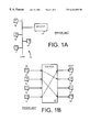
- FIG. 1A illustrates a prior-art LAN using a single collision domain.
- Network elements 12 include PCs and peripherals such as a workgroup printer.
- Each network element 12 contains a network-interface card (NIC) or equivalent that connects to the physical media, usually twisted-pair cable.
- NIC network-interface card
- While LAN 10 is often depicted as a single cable, often a repeater or hub is used. The cable from each network element 12 is plugged into the repeater box (not shown). The repeater then replicates a signal transmitted from one network element 12 to all other network elements 12 so that all network elements 12 receive the same transmission.
- LAN 10 Since each transmission is repeated to all other network elements 12 on LAN 10 , LAN 10 contains a single collision domain. Performance of LAN 10 is limited by collisions. Often a corporate network must be divided into many small LANs to limit collisions. Bridge 14 or a router is used to connect LAN 10 to other LANs or to a backbone network or wide-area network (WAN).
- WAN wide-area network
- FIG. 1B shows a LAN using a network switch to avoid large collision domains.
- Network elements 12 connect to switch 16 rather than to a repeater or hub.
- Each network element 12 is bi-directional (full-duplex) and is shown twice, once as an input to switch 16 and again as an output from switch 16 , but in reality each network element is a single element.
- Switch 16 monitors the inputs from each network element 12 , looking for a transmission. When a transmission to switch 16 is detected, the packet is parsed to determine the destination port. Switch 16 then makes a temporary connection from the input port to the output port and sends the packet to the destination port. The packet is sent only to the destination port and not to the other output ports.
- Switch 16 contains a switch fabric that allows multiple connections to be made at the same time. For example, input port (network element) A can send a packet to output port C, while input port B sends a packet to output port D. A collision does not occur even though both network elements A and B are transmitting at the same time. Switch 16 effectively creates separate collision domains for each pair of network elements during a packet transmission.
- Switch 16 can eliminate collisions, or break a network into smaller collision domains when entire LANs rather than single network elements are connected to the ports of switch 16 .
- switches have become enormous popular as a way to easily improve network performance.
- the original 10 Mbps Ethernet (10 Base-T) is being replaced with 100 Mbps Ethernet, and 1 Gbps Ethernet is expected.
- the higher speed networks require that the switches also transfer data at the higher rate to avoid congestion.
- the switches must also set up and tear down connections more rapidly.
- the switch fabric in network switches consists of a crossbar switch, which can simply be a matrix of transistor switches that connect each input port to every other output port.
- These crossbar switches are fast, but as more ports are added, the switch matrix grows exponentially as each new port must connect to all other ports. Thus switches with larger numbers of ports are expensive.
- Switches can also use a store-and-forward architecture. Incoming packets are stored in a memory and later read out to the output port. No switch matrix or crossbar switch is required. These store-and-forward switches can more easily add ports. However, memory bandwidth limits the speed and number of ports of these switches.
- the maximum throughput for a store-and-forward switch is when one half of the ports (n/2) are talking to the other half of the ports at full speed.
- the network speed is V (Mbps) per direction
- the number of memory access cycles A is 2, one cycle to write and one cycle to read.
- the required memory bandwidth S (Mbps) is:
- the memory must have a bandwidth of 200 M bytes/sec for a non-blocking switch with just 8 ports.
- a very fast memory with a 10-nanosecond access time must have a data-bus width of nearly 100 bits to meet such a bandwidth requirement.
- a switch-controller integrated circuit (IC) or chip would require 150 pins just for the memory interface.
- the 26 ports would require another 150 pins.
- the switch-controller chip could easily surpass 400 pins, making it very expensive. Using multiple chips further increases cost, power dissipation, and complexity of the switch system.
- SRAM static random-access memory
- DRAM dynamic-random-access memory
- DRAM dynamic-random-access memory
- the assignee has recognized the problem of bottlenecks to external dynamic-random-access memory (DRAM) in graphics display systems, and has pioneered embedded DRAM for graphics controllers. See for example: Puar et al., “Graphics Controller Integrated Circuit Without Memory Interface”, U.S. Pat. Nos. 5,650,955 and 5,703,806. These embedded-DRAM graphics controllers have been used predominantly for portable PC's such as laptop and notebook PCs.
- What is desired is a network switch for higher network speeds. It is desired to add ports without significantly increasing the cost of the switch.
- a network switch with a large number of high-speed ports is desired. It is desired to avoid increasingly larger numbers of pins on a network-switch chip as higher network speeds are used and higher s memory bandwidth is required.
- a high memory-bandwidth network switch is desired.
- a store-and-forward network switch with sufficient memory bandwidth and high port count for Gigabit networks is desired.
- a network switch chip has a plurality of input ports connected to external network nodes to receive packets.
- a plurality of output ports is connected to external network nodes. The output ports transmit the packets to the external network nodes.
- An embedded packet memory temporarily stores packets received from the input ports for transfer to the output ports for transmission.
- the embedded packet memory is a dynamic-random-access memory (DRAM) organized into rows and columns.
- DRAM dynamic-random-access memory
- An internal data bus is coupled to the embedded packet memory. It writes packets from the input ports to the embedded packet memory and reads the packets from the embedded packet memory to the output ports.
- the internal data bus is an internal bus without connection to external pins of the network switch chip during normal operating modes when packets are transmitted from input ports to output ports.
- Port controllers are coupled to the input ports and the output ports. They detect packets received at an input port and write the packet into the embedded packet memory over the internal data bus. They also read the packet from the embedded packet memory to an output port.
- a message bus is coupled to the port controllers. It sends a message from a port controller for an input port that receives a packet to a port controller for an output port that is a destination indicated by the packet. The message causes the port controller for the output port to read the packet from the embedded packet memory. Thus packets are switched from an input port to an output port by being written to and read from the embedded packet memory using the internal data bus in response to the message sent over the message bus.
- the message bus is further for sending an acknowledgement message from the port controller for the output port to the port controller for the input port when a packet has been read from the embedded packet memory.
- the port controller for the input port releases a memory space occupied by the packet in response to the acknowledgement message.
- memory space in the embedded packet memory is released when the acknowledgement message is sent over the message bus.
- the port controller for the input port writes an entire packet to a row of the embedded packet memory without interruption by other port controllers.
- Page-mode accesses to a same row in the embedded packet memory are faster than page-miss accesses to a different row in the embedded packet memory.
- the packet is written to the row in the embedded packet memory using mostly faster page-mode accesses.
- the internal data bus is a wide bus having at least 256 data bits.
- the internal data bus transfers at least 32 bytes of data for each memory-access cycle.
- the internal data bus is a wide interface between the input ports and the embedded packet memory.
- FIG. 1A illustrates a prior-art LAN using a single collision domain.
- FIG. 1B shows a LAN using a network switch to avoid large collision domains.
- FIG. 2 is a diagram of a store-and-forward network switch with an embedded DRAM and an internal token bus.
- FIG. 3 is a diagram of a switch chip with an internal packet memory showing more detail of port logic that send messages over an internal token bus.
- FIG. 4 shows the format of a message sent over the token bus.
- FIG. 5 shows in more detail a port controller that sends and receives messages over the token bus.
- FIG. 6 is a diagram of the write controller for an input port that writes the packet to the embedded DRAM packet memory.
- FIG. 7 is a diagram of the read controller for an output port that reads the packet from the embedded DRAM packet memory.
- FIG. 8 is a diagram of arbitration of port controllers accessing the embedded DRAM packet memory.
- FIG. 9 shows that packets are stored at DRAM-row boundaries in the embedded packet memory.
- FIG. 10 shows a switch chip with an embedded DRAM storing a packet memory and a routing table.
- the present invention relates to an improvement in network switches.
- the following description is presented to enable one of ordinary skill in the art to make and use the invention as provided in the context of a particular application and its requirements.
- Various modifications to the preferred embodiment will be apparent to those with skill in the art, and the general principles defined herein may be applied to other embodiments. Therefore, the present invention is not intended to be limited to the particular embodiments shown and described, but is to be accorded the widest scope consistent with the principles and novel features herein disclosed.
- the inventor has realized that as ports are added to a network switch, or as network speeds are increased, memory bandwidth requirements are substantially increased. Memory access times have been decreasing at a slower pace than the increase in Ethernet speeds. Thus higher bandwidth must come by increasing the bus width to the memory. However, increasing the memory bus width also increases pincount and I/O to an external memory.
- DRAM embedded dynamic-random-access memory
- DRAM embedded memory rather than a SRAM memory greatly increases the available memory depth.
- Large packets can be stored for many ports in the larger DRAM memory. These larger packets are preferred since they minimize network overhead and increase performance.
- the inventor has realized that the embedded DRAM can be organized so that a largest packet is stored within a single DRAM page. Faster page-mode access cycles can then be used to read or write the packet.
- the inventor has further realized that the higher bandwidth allows the entire packet to be read or written all at once resulting in sequential access of the DRAM, thus maximizing the use of page hit access cycles. Lower bandwidth memories might have unacceptably high latencies if entire packets were read without interruption.
- FIG. 2 is a diagram of a store-and-forward network switch with an embedded DRAM and an internal token bus for control.
- Network switch chip 18 is a store-and-forward switch that receives packets from one of four ports A, B, C, D, stores the packets in embedded DRAM packet memory 20 , and transmits the stored packets out to one or more of the four ports A, B, C, D.
- Port logic 22 , 24 , 26 , 28 are bi-directional ports to a network node connected to a computer, peripheral, LAN segment, or other network equipment such as another switch, router, repeater, bridge or hub. Packets may be input or output from any port.
- port logic 22 , 24 , 26 , 28 it first writes the packet into embedded DRAM packet memory 20 .
- a very wide bus is provided between port logic 22 , 24 , 26 , 28 and packet memory 20 .
- a 256-bit data bus may be used so that 32 bytes are transferred per memory-access cycle. When the memory-access cycle is 10 nanoseconds, the memory bandwidth is 3.2 Gbytes/sec.
- a message is sent from the input port logic to the output port logic. For example, when a packet is received on port A to be sent to port C, port logic 22 writes the packet into packet memory 20 and then sends a message to port logic 26 (port C). Port logic 26 responds by reading the packet from packet memory 20 and transmitting it out of switch chip 18 through port C. An acknowledgement message is then sent back from port C logic 26 to port A logic 22 . The acknowledgement message instructs port A to release the space used by the packet in packet memory 20 .
- Token bus 30 is another internal bus in switch chip 18 . Token bus 30 is not part of any external network and is simply used to pass internal messages from port to port within switch chip 18 .
- FIG. 3 is a diagram of a switch chip with an internal packet memory showing more detail of port logic that send messages over an internal token bus.
- Port A logic 22 and port B logic 24 are bi-directional, each having a receive first-in-first-out FIFO 32 and a transmit FIFO 34 that connect to a twisted pair through physical-layer transceivers.
- FIFOs 32 , 34 are relatively small, their purpose is to hold data and provide a bus conversion between the external interface such as Media Independent Interface (MII) or RMII and the internal bus.
- MII Media Independent Interface
- a data packet received through receive FIFO 32 is parsed by media-access-controller MAC 33 for the destination address.
- a table lookup may be performed in a routing table to determine which of the other ports in switch chip 18 to send the packet to.
- the received packets are then sent to receive packet buffer 36 and later written to embedded DRAM packet memory 20 .
- MAC 33 When port A is the output port, the packet written into packet memory 20 is read by port logic 22 into transmit packet buffer 38 . Then MAC 33 adds the low-level source address to the packet and transmits it out through transmit FIFO 34 to the external media. MAC 33 may perform other tasks such as checksum checking and generation and removing and adding low-level media-specific fields to the packet. MAC 33 may provide the packet header information to a packet processor for possible higher-layer processing.
- Packet buffers 36 , 38 are large enough to contain an entire packet, including the larger 1.5-Kbit packets. This allows for some flow control without data loss when the port cannot immediately write the packet into DRAM packet memory 20 , such as when another port is accessing the memory, or when DRAM refresh occurs.
- the packets are sent to DRAM packet memory over DRAM data bus 42 , which is a single data bus with 256 data lines (signals).
- Packet memory 20 is a low-cost single-port DRAM.
- Memory controller 94 receives requests (REQ) for memory access from port controller 40 in each port logic and replies with a grant acknowledgement (ACK) when a port is allowed access. Memory controller 94 generates the memory strobes and timing signals needed to transfer the data from packet buffer 36 over data bus 42 to DRAM packet memory 20 for write (input port), or from DRAM packet memory 20 over data bus 42 to packet buffer 38 on a read (output port).
- REQ requests
- ACK grant acknowledgement
- token bus 30 is shared among all port controllers 40 , collisions could occur as packets are received at random intervals.
- a token-passing scheme is used. All port controllers 40 are connected together in a ring or loop. Only one token is present at any time. This token is passed from port controller 40 to the next port controller 40 in the ring. A port may send a message over token bus 30 only when the port has the token. Thus only one port controller 40 may send a message over token bus 30 at any time.
- an input port When an input port has received a packet and written it to packet memory 20 , it must wait for the token to be passed around the ring to that port. Once the token is received, the port sends a message to the output port. This message includes the port number (A, B, C, D) of the output port and the row address within DRAM packet memory 20 where the packet is stored.
- the output port listens to all messages sent over token bus 30 . When a message matching its port number is detected, the row address from that message is stored by the output port's port controller 40 . The output port requests access to packet memory 20 . When memory controller 94 grants the output port access to packet memory 20 , the row address from the message is sent to memory controller 94 and the packet data is read from packet memory 20 into transmit packet buffer 38 of the output port. The packet is then passed through MAC 33 and transmit FIFO 34 to the output media.
- the output port sends an acknowledgement message over token bus 30 to the input port.
- This acknowledgement message instructs the input port to release the memory space used by the packet that was just transmitted.
- a centralized packet processor may also be present.
- the packet processor performs network management functions and policy decisions.
- a search engine for searching a network routing table can also be controlled by the packet processor.
- the packet processor can have a user interface to allow for policy and routing table changes.
- FIG. 4 shows the format of a message sent over the token bus.
- Message 50 begins with a fixed sequence of bits in start frame 44 , such as 7 one bits (7E Hex) for synchronization.
- the destination (output) port number (A, B, C, D) is contained in destination field 46 while the source (input) port-number is in field 47 .
- These are simple identifiers that indicates which of the switch chip's ports is the source or destination.
- the IP or MAC address is not included in the message.
- Packet type field 49 indicates if the packet is a normal (uni-cast) packet, multicast, or a broadcast packet sent to all ports. When the message is an acknowledgement message from the destination port back to the source port, packet type field 49 is set to 00.
- the row address of the packet in the DRAM packet memory is contained in row-address field 48 . Only the row address portion of the packet is sent in the message; the column address is assumed to begin at 0, since each packet is aligned to the DRAM row boundary. Sending just the row address and not the column address reduces the size of the message, improving token-bus performance.
- Length field 45 contains the packet length that is obtained from the packet header. Other fields can be included for policy information, such as an indication of the priority of the packet or the type of application that generated the packet.
- FIG. 5 shows in more detail a port controller that sends and receives messages over the token bus.
- Port controller 40 includes token controller 52 that communicates with token bus 30 , and write controller 54 and read controller 56 that control access to the embedded DRAM packet memory.
- write controller 54 When a new packet is received by the input port from the external media, write controller 54 sends a request to memory controller 94 , and when granted access to the packet memory, writes the packet to the packet memory. Write controller 54 sends a row address and increments a column address from zero to the packet length as the packet data is written to the DRAM packet memory. This way the packet is written to the embedded packet memory from the input port.
- Write controller 54 assigns one of the rows in the embedded packet memory to the new packet.
- a busy bit is set for an entry in the port's memory allocation table.
- the row address from this entry is the row address sent to memory controller 94 while the column address is incremented from zero to the packet length.
- write controller 54 sends the row address, packet length, and the destination port number to token controller 52 .
- token controller 52 keeps the token and sends a message over token bus 30 to the destination port.
- the message has the destination port number, packet length, and the row address from write controller 54 .
- Token controller 52 listens to all messages sent over token bus 30 . When the destination port field in a message matches the port number of the port controller, then the message is accepted. Other message are ignored, except for broadcast messages that are identified by a special broadcast message type.
- Token controller 52 sends the row address from the message to read controller 56 .
- Read controller 56 then sends a request to memory controller 94 , and when granted access to the packet memory, sends the row address and increments the column address from zero to the packet length. This way the packet is read from the embedded packet memory to the output port. The packet may then be transmitted to the external media.
- Token controller 52 sends the row address from the message to write controller 54 .
- Write controller 54 then clears the busy bit in the corresponding entry in its memory allocation table.
- FIG. 6 is a diagram of the write controller for an input port that writes the packet to the embedded DRAM packet memory.
- the embedded DRAM packet memory is divided into buffer regions, one for each input port.
- Each port's buffer region is further divided into DRAM rows, with each row for storing one packet.
- Input-port table 60 is a memory-allocation table with one entry for each row of the packet memory allocated to the port. Each entry contains the row address and a free/busy bit. When a new packet is written to the packet memory, the row address is taken from an entry in table 60 that has its free/busy bit cleared (free). The free/busy bit is then set to busy as the packet is written in to the packet memory. When number of packet entries reaches a programmable threshold, a flow-control-off message is sent to the sending device.
- the packet When the acknowledgement message is received from the output port, the packet has been read from the packet memory and no longer has to be stored.
- the freed row address from the acknowledgement message received from the token bus is latched into free row address register 64 , and then loaded in the table pointer with an offset that points to its location in the table.
- the free-busy bit is cleared to free for the matching entry. The row address can then be used for another new packet received from the external media.
- the packet memory is divided into regions for each input port.
- the row addresses for all rows in a port's region are sent as the memory configuration and latched into register 62 .
- mux 66 writes each configured row address to an entry in table 60 .
- Table pointer 68 is used to point to one of the entries for access.
- Write controller 54 then makes a request to the memory controller for access to the packet memory.
- the memory controller grants access to write controller 54
- the row address from row-address register 72 is sent to the memory controller along with a read/write (R/W) signal set to write.
- the column address is output from counter 74 .
- Counter 74 is incremented for each memory cycle until all the packet has been written, and counter 74 reaches the length of the packet.
- the actual packet length in bytes may be loaded into counter 74 , and only the upper bits of counter 74 sent as the column address.
- Counter 74 is incremented by the data-bus width for each memory cycle.
- the packet length is divided is by the DRAM data-bus width before being loaded into counter 74 .
- Counter 74 then increments by one for each memory access cycle until counter 74 reaches the packet length modulo the data-bus width.
- a 256-bit data bus writes 32 bytes for each memory cycle. For a packet length of 1.5 Kbyte, 48 memory cycles are required to write the entire packet.
- the column address from counter 74 indicates which column of 32 bytes is to be written in the current row from row-address register 72 .
- FIG. 7 is a diagram of the read controller for an output port that reads the packet from the embedded DRAM packet memory.
- Read controller 56 receives a message from the token bus that a packet is being sent from an input port. The row address from this message is stored in table 80 , along with the length of the packet. Table 80 acts as a simple FIFO or queue, allowing multiple input ports to send packets to the same output port, which processes the packets one at a time.
- Pointer 78 contains a write pointer and a read pointer.
- the write pointer points to an unused entry that should receive the next message's row address.
- the read pointer points to the next entry to be processed.
- the row address from this entry is loaded from table 80 to row-address register 82 , while the packet length is loaded into counter 84 . This packet length is loaded into counter 84 as the terminal count.
- Read controller 56 then makes a request to the memory controller for access to the packet memory.
- the memory controller grants access to read controller 56
- the row address from row-address register 82 is sent to the memory controller along with the read/write (R/W) signal set to read.
- the column address is output from counter 84 .
- Counter 84 is incremented for each memory cycle until all the packet has been read, and counter 84 reaches the length of the packet.
- the packet can be transmitted from the switch chip to the external media for the output port if it has not been flow-controlled off by the receiving device.
- the row address from row-address register 82 is then sent to the token controller.
- a message is formatted and sent to the input port with this row address, telling the input port that the packet has been sent and allowing the input port to release the row address in the packet memory.
- FIG. 8 is a diagram of arbitration of port controllers accessing the embedded DRAM packet memory.
- Port controller 40 send messages to each other over token bus 30 . These messages include row addresses in packet memory 20 where packets are stored. When a port controller needs to write a packet into memory 20 , or read a packet out of memory 20 , it must arbitrate for access to packet memory 20 since this memory is shared among all ports.
- Port controllers 40 send requests to arbiter 92 when memory access is needed.
- Refresh controller 90 also must have periodic access to packet memory 20 to perform refresh operations so that data is not lost.
- Arbiter 92 receives all requests and grants access to one port controller 40 at a time. When refresh controller 90 is granted access, no port controller may access memory 20 .
- Arbiter 92 uses a round-robin arbitration scheme.
- Network policy can be implemented to prioritize important packets such as for voice or videoconferencing applications. These high-priority packets can have their port controller 40 signal arbiter 92 , which then grants the port immediate or higher-priority access.
- Arbiter 92 informs memory controller 94 of which port controller 40 has won arbitration. Memory controller 94 then generates timing signals to embedded DRAM packet memory 20 for each memory cycle until the port controller indicates that it has finished. Port controllers are not preempted. Instead, each port controller continues to access packet memory 20 until the entire packet has been read or written. Since the packet is located within a single row of the DRAM, most of these access cycles are the more efficient page-mode row-hit cycles, increasing performance.
- FIG. 9 shows that packets are stored at DRAM-row boundaries in the embedded packet memory.
- the DRAM memory cells in packet memory 20 are arranged into an array of rows and columns.
- the row address is sent to the DRAM first, followed by the column address, which is the address within a row.
- a row of cells is known as a DRAM page, and accesses to other cells in the same row are faster than accesses to other rows. Accesses within the same row are known as page-mode hit cycles, while accesses to other DRAM rows are known as row miss cycles or precharge cycles. A longer access time is needed when changing to a different row since a period of time known as a row precharge is needed before the cells can be read.
- Each column in the DRAM array is the width of the data bus, 256 bits or 32 bytes.
- Each page-hit memory-access cycle reads one column, or 32 bytes.
- the memory array has a total of 48 columns, which makes each row contains 32 ⁇ 48 bytes, or 1.5 Kbytes. Since 1.5 Kbytes is the size of the largest packet, an entire packet can fit within a single row. Each row can contain a different packet.
- the first memory cycle is a page-miss cycle requiring 6 clock cycles, while all the other cycles are page hit cycles requiring one clock each.
- This arrangement of the packets in DRAM rows is very efficient since mostly DRAM page hit cycles are used.
- the packet memory is divided into several regions, one for each input port. Output ports are not assigned any memory space.
- the region for port A includes rows 1 , 2 , 3 , 4
- the region for port C contains rows 34 , 35 , 36 , 37 .
- ports A and C can buffer up to 4 packets each, since each has 4 rows allocated in the embedded packet memory.
- Packet 1 received by port A is written into row 1 . Since this is a small packet of 64 bytes, it occupies only the first two columns. The other 46 columns in row 1 are not used.
- the next packet received by port A is packet 2 , which is stored in row 2 . Packet 2 is somewhat larger, occupying the first 4 columns (128 bytes).
- Packet 3 is a 1.5-Kbyte packet and occupies the entire row 3 , all 48 columns. Row 4 is unused but will receive the next packet input to port A.
- Port C has received two packets.
- Packet 6 is another large 1.5-Kbyte packet, and occupies all 48 columns of row 34 .
- Packet 7 is a small 64-byte packet and occupies just the first 2 columns. Columns 3-48 of row 35 are unused. Some rows of packet memory 20 can be reserved for management functions.
- FIG. 10 shows a switch chip with an embedded DRAM storing a packet memory and a packet processor that includes a routing table for multi-layer processing.
- Network switch chip 18 is a store-and-forward switch that receives packets from one of four ports A, B, C, D, stores the packets in embedded DRAM packet memory 20 , and transmits the stored packets out another of the four ports A, B, C, D.
- Packet processor 100 is also coupled to token bus 30 .
- Packet processor 100 receives IP, MAC or other header parameters (addresses) from port controller for packets that have been received.
- a special message can be used to send processing requests to packet processor 100 , and for packet processor 100 to send the results back to the port controller.
- Packet processor 100 compares the IP or MAC address to IP or MAC addresses stored in entries in routing table 102 and performs policy (filter) processing. When instructions are sent through the token bus to the output port controller whether the packet should be sent through that port to reach its final destination.
- Routing table 102 in packet processor 100 contains entries for network policy or filters with IP or MAC addresses and the port number on switch chip 18 that is the next hop to that IP or MAC address.
- Port logic 22 , 24 , 26 , 28 When a packet is received by port logic 22 , 24 , 26 , 28 , it first writes the packet into embedded DRAM packet memory 20 . Once the packet has been written into packet memory 20 , a message is sent from the input port logic to the output port logic via packet processor with appropriate policy application instructions. Port logic 26 responds by reading the packet from packet memory 20 and transmitting it out of switch chip 18 through port C. An acknowledgement message is then sent back from port C logic 26 to port A logic 22 . The messages are sent among port logic 22 , 24 , 26 , 28 over token bus 30 . Token bus 30 is another internal bus in switch chip 18 .
- a network switch with shared embedded DRAM is ideally suited for higher network speeds such as 100 Mbps, 1 Gbps and beyond. Ports can be added without significantly increasing the cost of the switch.
- the network switch can support a large number of high-speed ports. Increasingly larger numbers of pins for external memory access on a network-switch chip are avoided as higher network speeds are used and higher memory bandwidth is required.
- a high memory-bandwidth network switch uses a store-and-forward memory with sufficient memory bandwidth for 1 Gbps networks.
- Memory bandwidth can be increased by increasing the width of the internal bus without increasing a number of external I/O pins on the IC package.
- a 256-bit-wide internal DRAM produces a bandwidth in excess of 3 Gbytes/sec. This is a sufficiently large bandwidth to achieve a 128-port 100 Mbps network switch or a 12-port 1-Gbps switch.
- DRAM embedded memory rather than an external SRAM memory greatly increases the available memory depth. Large packets can be stored for many ports in the larger DRAM memory. These larger packets are preferred since they minimize network overhead and increase performance.
- the embedded DRAM is organized so that a 64-byte or 1.5K packet is stored within a single DRAM page. Faster page-mode access cycles are used to read or write the packet. The higher bandwidth allows the entire packet to be read or written all at once, maximizing the use of page hit access cycles.
- the invention's architecture allows for scalability of the design such that number of ports, memory size, and the bus width can be scaled and optimized for the application.
- the architecture also allows a design of a simple Layer- 2 -only switch or a more complex multi-layered (layers 3 - 7 ) switch. Embedding the packet memory with control logic reduces power dissipation of the overall system. Integrating packet memory and the packet processor on the same chip makes network-policy applications at wire speed possible, thus increasing system throughput.
- the invention can be used for store-and-forward cell Switching, where each cell can be stored in the embedded DRAM page.
- Dynamic registers or latches may be used for entry registers.
- FIFO buffers or pipeline latches can be inserted into the circuitry at many points, such as to and from the embedded memory.
- Multiple tables or banks of embedded DRAM with different contents can be used to perform searches as well as store packets.
- the embedded DRAM may be integrated on a same silicon substrate with the parallel search engines. Other kinds of substrates may be substituted.
- Port controllers can be designed for varying data rates such as 10 Mbit, 100 Mbit, 1 Gbit or higher.
- a high-speed port such as a 1-Gbit port may be used for an uplink for port aggregation and/or for cascading these chips to achieve higher port count.
- a 2.4 Gbit (OC 48 ) port may also be providing for connection to a wide-area network (WAN).
- the input port numbers can be assigned in such a way that they form the MSB's of the absolute row address. This reduces the number of bits required for the row address transferred across the token bus.
- Test mode hardware may be added to connect the internal data bus to external I/O pins for testing the embedded packet memory.
- the data bus may be compressed using a signature generator or analyzer or other test logic before being sent off-chip.
- the internal data bus is not connected to the external I/O pins.
- any test-mode connection of the internal data bus to external pins is not considered a true connection to external pins since the normal function of the external pins must be halted to pass the test data.
- the DRAM row size can be varied from 8 columns to 64 to fit the requirement of the application. Many logic and firmware implementations are possible for the controllers. Other kinds of networks besides Ethernet can benefit from the invention. Different numbers of ports can be used with the switch chip, and some ports can be unidirectional.
- the switch chip can be used for LANs or in higher-speed backbone networks.
- the format of the messages can be changes and fields added for network management and policy control.
- the message or token bus can also use other control schemes besides token passing. Daisy chaining or a centralized arbiter can be used to control access to the token bus.
- the token bus may be further sub-divided as well.
Abstract
Description


Claims (20)
Priority Applications (1)
| Application Number | Priority Date | Filing Date | Title |
|---|---|---|---|
| US09/251,721 US6424658B1 (en) | 1999-01-29 | 1999-02-17 | Store-and-forward network switch using an embedded DRAM |
Applications Claiming Priority (2)
| Application Number | Priority Date | Filing Date | Title |
|---|---|---|---|
| US09/240,726 US6308220B1 (en) | 1999-01-29 | 1999-01-29 | Circulating parallel-search engine with random inputs for network routing table stored in a wide embedded DRAM |
| US09/251,721 US6424658B1 (en) | 1999-01-29 | 1999-02-17 | Store-and-forward network switch using an embedded DRAM |
Related Parent Applications (1)
| Application Number | Title | Priority Date | Filing Date |
|---|---|---|---|
| US09/240,726 Continuation-In-Part US6308220B1 (en) | 1999-01-29 | 1999-01-29 | Circulating parallel-search engine with random inputs for network routing table stored in a wide embedded DRAM |
Publications (1)
| Publication Number | Publication Date |
|---|---|
| US6424658B1 true US6424658B1 (en) | 2002-07-23 |
Family
ID=46276327
Family Applications (1)
| Application Number | Title | Priority Date | Filing Date |
|---|---|---|---|
| US09/251,721 Expired - Lifetime US6424658B1 (en) | 1999-01-29 | 1999-02-17 | Store-and-forward network switch using an embedded DRAM |
Country Status (1)
| Country | Link |
|---|---|
| US (1) | US6424658B1 (en) |
Cited By (116)
| Publication number | Priority date | Publication date | Assignee | Title |
|---|---|---|---|---|
| US20020009079A1 (en) * | 2000-06-23 | 2002-01-24 | Jungck Peder J. | Edge adapter apparatus and method |
| US20020097713A1 (en) * | 2000-11-17 | 2002-07-25 | Andrew Chang | Backplane interface adapter |
| US20020181456A1 (en) * | 2001-05-31 | 2002-12-05 | Fujitsu Limited | Switch device and data transfer system |
| US20020188752A1 (en) * | 2001-05-04 | 2002-12-12 | Tomassetti Stephen Robert | Control messaging for an entertainment and communications network |
| US20020194291A1 (en) * | 2001-05-15 | 2002-12-19 | Zahid Najam | Apparatus and method for interfacing with a high speed bi-directional network |
| US20030009651A1 (en) * | 2001-05-15 | 2003-01-09 | Zahid Najam | Apparatus and method for interconnecting a processor to co-processors using shared memory |
| US20030016683A1 (en) * | 1999-12-10 | 2003-01-23 | George William R. | Fibre channel credit extender and repeater |
| US6618390B1 (en) * | 1999-05-21 | 2003-09-09 | Advanced Micro Devices, Inc. | Method and apparatus for maintaining randomly accessible free buffer information for a network switch |
| US20030179748A1 (en) * | 2000-06-05 | 2003-09-25 | George William R. | Hardware-enforced loop-level hard zoning for fibre channel switch fabric |
| US6667983B1 (en) * | 1999-05-27 | 2003-12-23 | 3Com Corporation | Scaleable priority arbiter for arbitrating between multiple FIFO entry points of a network interface card |
| US6674805B1 (en) | 2000-05-02 | 2004-01-06 | Ati Technologies, Inc. | System for controlling a clock signal for synchronizing a counter to a received value and method thereof |
| US20040013092A1 (en) * | 2002-07-22 | 2004-01-22 | Betker Steven Manning | Method and system for dynamically assigning domain identification in a multi-module fibre channel switch |
| US20040013125A1 (en) * | 2002-07-22 | 2004-01-22 | Betker Steven Manning | Method and system for primary blade selection in a multi-module fibre channel switch |
| US6683602B1 (en) * | 1999-11-30 | 2004-01-27 | Seiko Epson Corporation | Display control apparatus and electronic appliance |
| US6693914B1 (en) * | 1999-10-01 | 2004-02-17 | Stmicroelectronics, Inc. | Arbitration mechanism for packet transmission |
| US6697359B1 (en) * | 1999-07-02 | 2004-02-24 | Ancor Communications, Inc. | High performance switch fabric element and switch systems |
| US6741591B1 (en) * | 1999-11-03 | 2004-05-25 | Cisco Technology, Inc. | Search engine interface system and method |
| US20040109365A1 (en) * | 2002-12-10 | 2004-06-10 | Isic Corporation | Methods and apparatus for data storage and retrieval |
| US6763390B1 (en) | 2000-01-24 | 2004-07-13 | Ati Technologies, Inc. | Method and system for receiving and framing packetized data |
| US6771532B2 (en) * | 1994-06-20 | 2004-08-03 | Neomagic Corporation | Graphics controller integrated circuit without memory interface |
| US6778533B1 (en) | 2000-01-24 | 2004-08-17 | Ati Technologies, Inc. | Method and system for accessing packetized elementary stream data |
| US6785336B1 (en) | 2000-01-24 | 2004-08-31 | Ati Technologies, Inc. | Method and system for retrieving adaptation field data associated with a transport packet |
| US20040179548A1 (en) * | 2000-11-17 | 2004-09-16 | Andrew Chang | Method and system for encoding wide striped cells |
| US6804731B1 (en) * | 2000-08-11 | 2004-10-12 | Paion Company, Limited | System, method and article of manufacture for storing an incoming datagram in switch matrix in a switch fabric chipset system |
| US6804266B1 (en) | 2000-01-24 | 2004-10-12 | Ati Technologies, Inc. | Method and apparatus for handling private data from transport stream packets |
| US20040215869A1 (en) * | 2002-01-23 | 2004-10-28 | Adisak Mekkittikul | Method and system for scaling memory bandwidth in a data network |
| US6836813B1 (en) * | 2001-11-30 | 2004-12-28 | Advanced Micro Devices, Inc. | Switching I/O node for connection in a multiprocessor computer system |
| US20050013609A1 (en) * | 2003-07-16 | 2005-01-20 | Fike John M. | Method and system for minimizing disruption in common-access networks |
| US20050015517A1 (en) * | 2003-07-16 | 2005-01-20 | Fike Melanie A. | Method and apparatus for improving buffer utilization in communication networks |
| US20050025060A1 (en) * | 2003-07-16 | 2005-02-03 | Fike John M. | Method and apparatus for testing loop pathway integrity in a fibre channel arbitrated loop |
| US20050024367A1 (en) * | 2000-12-13 | 2005-02-03 | William Radke | Memory system and method for improved utilization of read and write bandwidth of a graphics processing system |
| US20050060420A1 (en) * | 2003-09-11 | 2005-03-17 | Kovacevic Branko D. | System for decoding multimedia data and method thereof |
| US20050066133A1 (en) * | 2003-09-18 | 2005-03-24 | Silicon Aquarius, Inc. | Memories for electronic systems |
| US20050066144A1 (en) * | 2003-09-18 | 2005-03-24 | International Business Machines Corporation | Methods and apparatus for allocating bandwidth for a network processor |
| US20050083930A1 (en) * | 2003-10-20 | 2005-04-21 | Jen-Kai Chen | Method of early buffer release and associated MAC controller |
| US6885680B1 (en) | 2000-01-24 | 2005-04-26 | Ati International Srl | Method for synchronizing to a data stream |
| US6886141B1 (en) | 2002-10-07 | 2005-04-26 | Qlogic Corporation | Method and system for reducing congestion in computer networks |
| US20050089049A1 (en) * | 2001-05-15 | 2005-04-28 | Foundry Networks, Inc. | High-performance network switch |
| US6901072B1 (en) * | 2003-05-15 | 2005-05-31 | Foundry Networks, Inc. | System and method for high speed packet transmission implementing dual transmit and receive pipelines |
| US6912202B1 (en) * | 2001-01-25 | 2005-06-28 | Advanced Micro Device, Inc. | Arrangement for testing network switch expansion port using external logic to emulate connected expansion port |
| US6917623B1 (en) * | 2001-03-26 | 2005-07-12 | Advanced Micro Devices, Inc. | System and method for transferring data in a network device |
| US20050238353A1 (en) * | 2004-04-23 | 2005-10-27 | Mcglaughlin Edward C | Fibre channel transparent switch for mixed switch fabrics |
| US6981027B1 (en) * | 2000-04-10 | 2005-12-27 | International Business Machines Corporation | Method and system for memory management in a network processing system |
| US6988238B1 (en) | 2000-01-24 | 2006-01-17 | Ati Technologies, Inc. | Method and system for handling errors and a system for receiving packet stream data |
| US20060020725A1 (en) * | 2004-07-20 | 2006-01-26 | Dropps Frank R | Integrated fibre channel fabric controller |
| US6999424B1 (en) | 2000-01-24 | 2006-02-14 | Ati Technologies, Inc. | Method for displaying data |
| US20060075165A1 (en) * | 2004-10-01 | 2006-04-06 | Hui Ben K | Method and system for processing out of order frames |
| US7103504B1 (en) | 2003-11-21 | 2006-09-05 | Qlogic Corporation | Method and system for monitoring events in storage area networks |
| US7114008B2 (en) | 2000-06-23 | 2006-09-26 | Cloudshield Technologies, Inc. | Edge adapter architecture apparatus and method |
| US7187687B1 (en) | 2002-05-06 | 2007-03-06 | Foundry Networks, Inc. | Pipeline method and system for switching packets |
| US7266117B1 (en) | 2002-05-06 | 2007-09-04 | Foundry Networks, Inc. | System architecture for very fast ethernet blade |
| US20070248115A1 (en) * | 2006-04-21 | 2007-10-25 | Pesa Switching Systems, Inc. | Distributed routing system and method |
| US7334046B1 (en) | 2002-08-05 | 2008-02-19 | Qlogic, Corporation | System and method for optimizing frame routing in a network |
| US7352701B1 (en) | 2003-09-19 | 2008-04-01 | Qlogic, Corporation | Buffer to buffer credit recovery for in-line fibre channel credit extension devices |
| US7356030B2 (en) | 2000-11-17 | 2008-04-08 | Foundry Networks, Inc. | Network switch cross point |
| US20080086577A1 (en) * | 2006-10-04 | 2008-04-10 | Mediatek Inc. | Digital Television System, Memory Controller, and Method for Data Access |
| US7362717B1 (en) | 2002-10-03 | 2008-04-22 | Qlogic, Corporation | Method and system for using distributed name servers in multi-module fibre channel switches |
| US20080095152A1 (en) * | 2000-06-05 | 2008-04-24 | Qlogic Switch Products, Inc. | Hardware-enforced loop and npiv hard zoning for fibre channel switch fabric |
| US7366961B1 (en) | 2000-01-24 | 2008-04-29 | Ati Technologies, Inc. | Method and system for handling errors |
| US7397768B1 (en) | 2002-09-11 | 2008-07-08 | Qlogic, Corporation | Zone management in a multi-module fibre channel switch |
| US7406092B2 (en) | 2003-07-21 | 2008-07-29 | Qlogic, Corporation | Programmable pseudo virtual lanes for fibre channel systems |
| US7411958B2 (en) | 2004-10-01 | 2008-08-12 | Qlogic, Corporation | Method and system for transferring data directly between storage devices in a storage area network |
| US7420982B2 (en) | 2003-07-21 | 2008-09-02 | Qlogic, Corporation | Method and system for keeping a fibre channel arbitrated loop open during frame gaps |
| US7426572B1 (en) * | 2001-10-31 | 2008-09-16 | Juniper Networks, Inc. | Network router using embedded and external memory based on packet destination |
| US20080231900A1 (en) * | 2002-06-19 | 2008-09-25 | Canon Kabushiki Kaisha | Information processing apparatus |
| US7430175B2 (en) | 2003-07-21 | 2008-09-30 | Qlogic, Corporation | Method and system for managing traffic in fibre channel systems |
| US7463646B2 (en) | 2003-07-16 | 2008-12-09 | Qlogic Corporation | Method and system for fibre channel arbitrated loop acceleration |
| US7466700B2 (en) | 2003-07-21 | 2008-12-16 | Qlogic, Corporation | LUN based hard zoning in fibre channel switches |
| US7468975B1 (en) | 2002-05-06 | 2008-12-23 | Foundry Networks, Inc. | Flexible method for processing data packets in a network routing system for enhanced efficiency and monitoring capability |
| US7471635B2 (en) | 2003-07-16 | 2008-12-30 | Qlogic, Corporation | Method and apparatus for test pattern generation |
| US7474660B1 (en) * | 1999-03-31 | 2009-01-06 | Cisco Technology, Inc. | MAC address extension to maintain router information in source routed computer networks |
| US7480293B2 (en) | 2004-02-05 | 2009-01-20 | Qlogic, Corporation | Method and system for preventing deadlock in fibre channel fabrics using frame priorities |
| US7502366B1 (en) * | 2000-05-23 | 2009-03-10 | Advanced Micro Devices, Inc. | Arrangement in a network switch for prioritizing data frames based on user-defined frame attributes |
| US7512067B2 (en) | 2003-07-21 | 2009-03-31 | Qlogic, Corporation | Method and system for congestion control based on optimum bandwidth allocation in a fibre channel switch |
| US20090100500A1 (en) * | 2007-10-15 | 2009-04-16 | Foundry Networks, Inc. | Scalable distributed web-based authentication |
| US7548560B1 (en) | 2006-02-27 | 2009-06-16 | Qlogic, Corporation | Method and system for checking frame-length in fibre channel frames |
| US7596139B2 (en) | 2000-11-17 | 2009-09-29 | Foundry Networks, Inc. | Backplane interface adapter with error control and redundant fabric |
| US20090262741A1 (en) * | 2000-06-23 | 2009-10-22 | Jungck Peder J | Transparent Provisioning of Services Over a Network |
| US7613816B1 (en) | 2006-11-15 | 2009-11-03 | Qlogic, Corporation | Method and system for routing network information |
| US20090276556A1 (en) * | 2006-10-04 | 2009-11-05 | Mediatek Inc. | Memory controller and method for writing a data packet to or reading a data packet from a memory |
| US7646767B2 (en) | 2003-07-21 | 2010-01-12 | Qlogic, Corporation | Method and system for programmable data dependant network routing |
| US7649885B1 (en) | 2002-05-06 | 2010-01-19 | Foundry Networks, Inc. | Network routing system for enhanced efficiency and monitoring capability |
| US7657703B1 (en) | 2004-10-29 | 2010-02-02 | Foundry Networks, Inc. | Double density content addressable memory (CAM) lookup scheme |
| US7668186B1 (en) * | 2006-03-07 | 2010-02-23 | Xilinx, Inc. | Token ecosystem for buffer management |
| US7669190B2 (en) | 2004-05-18 | 2010-02-23 | Qlogic, Corporation | Method and system for efficiently recording processor events in host bus adapters |
| US7684401B2 (en) | 2003-07-21 | 2010-03-23 | Qlogic, Corporation | Method and system for using extended fabric features with fibre channel switch elements |
| US7792115B2 (en) | 2003-07-21 | 2010-09-07 | Qlogic, Corporation | Method and system for routing and filtering network data packets in fibre channel systems |
| US7813365B2 (en) | 2000-12-19 | 2010-10-12 | Foundry Networks, Inc. | System and method for router queue and congestion management |
| US7817659B2 (en) | 2004-03-26 | 2010-10-19 | Foundry Networks, Llc | Method and apparatus for aggregating input data streams |
| US7848253B2 (en) | 1999-01-12 | 2010-12-07 | Mcdata Corporation | Method for scoring queued frames for selective transmission through a switch |
| US7894348B2 (en) | 2003-07-21 | 2011-02-22 | Qlogic, Corporation | Method and system for congestion control in a fibre channel switch |
| US7903654B2 (en) | 2006-08-22 | 2011-03-08 | Foundry Networks, Llc | System and method for ECMP load sharing |
| US7930377B2 (en) | 2004-04-23 | 2011-04-19 | Qlogic, Corporation | Method and system for using boot servers in networks |
| US7978614B2 (en) | 2007-01-11 | 2011-07-12 | Foundry Network, LLC | Techniques for detecting non-receipt of fault detection protocol packets |
| US20110176421A1 (en) * | 2008-08-19 | 2011-07-21 | Check Point Software Technologies Ltd. | Methods for intelligent nic bonding and load-balancing |
| US8037399B2 (en) | 2007-07-18 | 2011-10-11 | Foundry Networks, Llc | Techniques for segmented CRC design in high speed networks |
| US8090901B2 (en) | 2009-05-14 | 2012-01-03 | Brocade Communications Systems, Inc. | TCAM management approach that minimize movements |
| US8149839B1 (en) | 2007-09-26 | 2012-04-03 | Foundry Networks, Llc | Selection of trunk ports and paths using rotation |
| US8238255B2 (en) | 2006-11-22 | 2012-08-07 | Foundry Networks, Llc | Recovering from failures without impact on data traffic in a shared bus architecture |
| US8260109B2 (en) | 2000-11-06 | 2012-09-04 | Ati Technologies Ulc | System for digital time shifting and method thereof |
| US8271859B2 (en) | 2007-07-18 | 2012-09-18 | Foundry Networks Llc | Segmented CRC design in high speed networks |
| US20120253780A1 (en) * | 2011-03-28 | 2012-10-04 | Ramanjaneyulu Talla | Systems and methods for emulating a nic for packet transmission on hardware rss unaware nics in a multi-core system |
| US8284845B1 (en) | 2000-01-24 | 2012-10-09 | Ati Technologies Ulc | Method and system for handling data |
| US8295299B2 (en) | 2004-10-01 | 2012-10-23 | Qlogic, Corporation | High speed fibre channel switch element |
| US8428061B1 (en) * | 2001-11-27 | 2013-04-23 | Marvell Israel (M.I.S.L) Ltd. | Packet header altering device |
| US8448162B2 (en) | 2005-12-28 | 2013-05-21 | Foundry Networks, Llc | Hitless software upgrades |
| US8464238B1 (en) | 2006-01-31 | 2013-06-11 | Qlogic, Corporation | Method and system for managing storage area networks |
| US20130258892A1 (en) * | 2010-02-15 | 2013-10-03 | Texas Instruments Incorporated | Wireless Chip-to-Chip Switching |
| US8599850B2 (en) | 2009-09-21 | 2013-12-03 | Brocade Communications Systems, Inc. | Provisioning single or multistage networks using ethernet service instances (ESIs) |
| US8671219B2 (en) | 2002-05-06 | 2014-03-11 | Foundry Networks, Llc | Method and apparatus for efficiently processing data packets in a computer network |
| US8730961B1 (en) | 2004-04-26 | 2014-05-20 | Foundry Networks, Llc | System and method for optimizing router lookup |
| US8850137B2 (en) | 2010-10-11 | 2014-09-30 | Cisco Technology, Inc. | Memory subsystem for counter-based and other applications |
| US9444785B2 (en) | 2000-06-23 | 2016-09-13 | Cloudshield Technologies, Inc. | Transparent provisioning of network access to an application |
| US10732866B2 (en) | 2016-10-27 | 2020-08-04 | Samsung Electronics Co., Ltd. | Scaling out architecture for DRAM-based processing unit (DPU) |
| US20210334224A1 (en) * | 2015-03-30 | 2021-10-28 | Marvell Asia Pte., Ltd. | Packet processing system, method and device utilizing a port client chain |
| EP4068703A1 (en) * | 2021-03-31 | 2022-10-05 | Mitsubishi Electric R&D Centre Europe B.V. | Method and device for performing software-based switching functions in a local area network |
Citations (27)
| Publication number | Priority date | Publication date | Assignee | Title |
|---|---|---|---|---|
| US5371870A (en) * | 1992-04-24 | 1994-12-06 | Digital Equipment Corporation | Stream buffer memory having a multiple-entry address history buffer for detecting sequential reads to initiate prefetching |
| US5521923A (en) | 1993-08-27 | 1996-05-28 | Alcatel Sel Aktiengesellschaft | Method and facility for temporarily storing data packets, and exchange with such a facility |
| US5555264A (en) | 1992-03-20 | 1996-09-10 | Telefoanktiebolaget Lm Ericsson | Methods and devices for prioritizing in handling buffers in packet networks |
| US5610921A (en) * | 1995-08-31 | 1997-03-11 | Sun Microsystems, Inc. | Scalable architecture for asynchronous transfer mode segmentation and reassembly |
| US5625625A (en) | 1995-07-07 | 1997-04-29 | Sun Microsystems, Inc. | Method and apparatus for partitioning data load and unload functions within an interface system for use with an asynchronous transfer mode system |
| US5633865A (en) | 1995-03-31 | 1997-05-27 | Netvantage | Apparatus for selectively transferring data packets between local area networks |
| US5633876A (en) | 1992-10-26 | 1997-05-27 | Eon Corporation | Store and forward repeater |
| US5703806A (en) | 1994-06-20 | 1997-12-30 | Neomagic Corporation | Graphics controller integrated circuit without memory interface |
| US5704059A (en) * | 1995-07-28 | 1997-12-30 | Nec Corporation | Method of write to graphic memory where memory cells designated by plurality of addresses selected simultaneously for one row address are written |
| US5734921A (en) * | 1990-11-13 | 1998-03-31 | International Business Machines Corporation | Advanced parallel array processor computer package |
| US5740175A (en) | 1995-10-03 | 1998-04-14 | National Semiconductor Corporation | Forwarding database cache for integrated switch controller |
| US5742765A (en) * | 1996-06-19 | 1998-04-21 | Pmc-Sierra, Inc. | Combination local ATM segmentation and reassembly and physical layer device |
| US5802054A (en) | 1996-08-15 | 1998-09-01 | 3Com Corporation | Atomic network switch with integrated circuit switch nodes |
| US5809024A (en) | 1995-07-12 | 1998-09-15 | Bay Networks, Inc. | Memory architecture for a local area network module in an ATM switch |
| US5854792A (en) | 1995-09-12 | 1998-12-29 | Kabushiki Kaisha Toshiba | Network connection apparatus |
| US5864539A (en) | 1996-05-06 | 1999-01-26 | Bay Networks, Inc. | Method and apparatus for a rate-based congestion control in a shared memory switch |
| US5926473A (en) * | 1994-09-12 | 1999-07-20 | Amber Wave Systems, Inc. | Distributed processing ethernet switch with adaptive cut-through switching |
| US5963746A (en) * | 1990-11-13 | 1999-10-05 | International Business Machines Corporation | Fully distributed processing memory element |
| US5963745A (en) * | 1990-11-13 | 1999-10-05 | International Business Machines Corporation | APAP I/O programmable router |
| US6011798A (en) * | 1997-08-15 | 2000-01-04 | Intel Corporation | Adaptive transmit rate control scheduler |
| US6094715A (en) * | 1990-11-13 | 2000-07-25 | International Business Machine Corporation | SIMD/MIMD processing synchronization |
| US6122279A (en) * | 1995-10-02 | 2000-09-19 | Virata Limited | Asynchronous transfer mode switch |
| US6125421A (en) * | 1994-11-30 | 2000-09-26 | Hitachi Micro Systems, Inc. | Independent multichannel memory architecture |
| US6141336A (en) * | 1996-12-13 | 2000-10-31 | International Business Machines Corporation | Traffic scheduling method, system and article of manufacture for a wireless access to an asynchronous transfer mode network |
| US6157978A (en) * | 1998-09-16 | 2000-12-05 | Neomagic Corp. | Multimedia round-robin arbitration with phantom slots for super-priority real-time agent |
| US6205149B1 (en) * | 1997-09-11 | 2001-03-20 | 3Com Corporation | Quality of service control mechanism and apparatus |
| US6308220B1 (en) * | 1999-01-29 | 2001-10-23 | Neomagic Corp. | Circulating parallel-search engine with random inputs for network routing table stored in a wide embedded DRAM |
-
1999
- 1999-02-17 US US09/251,721 patent/US6424658B1/en not_active Expired - Lifetime
Patent Citations (27)
| Publication number | Priority date | Publication date | Assignee | Title |
|---|---|---|---|---|
| US6094715A (en) * | 1990-11-13 | 2000-07-25 | International Business Machine Corporation | SIMD/MIMD processing synchronization |
| US5963745A (en) * | 1990-11-13 | 1999-10-05 | International Business Machines Corporation | APAP I/O programmable router |
| US5963746A (en) * | 1990-11-13 | 1999-10-05 | International Business Machines Corporation | Fully distributed processing memory element |
| US5734921A (en) * | 1990-11-13 | 1998-03-31 | International Business Machines Corporation | Advanced parallel array processor computer package |
| US5555264A (en) | 1992-03-20 | 1996-09-10 | Telefoanktiebolaget Lm Ericsson | Methods and devices for prioritizing in handling buffers in packet networks |
| US5371870A (en) * | 1992-04-24 | 1994-12-06 | Digital Equipment Corporation | Stream buffer memory having a multiple-entry address history buffer for detecting sequential reads to initiate prefetching |
| US5633876A (en) | 1992-10-26 | 1997-05-27 | Eon Corporation | Store and forward repeater |
| US5521923A (en) | 1993-08-27 | 1996-05-28 | Alcatel Sel Aktiengesellschaft | Method and facility for temporarily storing data packets, and exchange with such a facility |
| US5703806A (en) | 1994-06-20 | 1997-12-30 | Neomagic Corporation | Graphics controller integrated circuit without memory interface |
| US5926473A (en) * | 1994-09-12 | 1999-07-20 | Amber Wave Systems, Inc. | Distributed processing ethernet switch with adaptive cut-through switching |
| US6125421A (en) * | 1994-11-30 | 2000-09-26 | Hitachi Micro Systems, Inc. | Independent multichannel memory architecture |
| US5633865A (en) | 1995-03-31 | 1997-05-27 | Netvantage | Apparatus for selectively transferring data packets between local area networks |
| US5625625A (en) | 1995-07-07 | 1997-04-29 | Sun Microsystems, Inc. | Method and apparatus for partitioning data load and unload functions within an interface system for use with an asynchronous transfer mode system |
| US5809024A (en) | 1995-07-12 | 1998-09-15 | Bay Networks, Inc. | Memory architecture for a local area network module in an ATM switch |
| US5704059A (en) * | 1995-07-28 | 1997-12-30 | Nec Corporation | Method of write to graphic memory where memory cells designated by plurality of addresses selected simultaneously for one row address are written |
| US5610921A (en) * | 1995-08-31 | 1997-03-11 | Sun Microsystems, Inc. | Scalable architecture for asynchronous transfer mode segmentation and reassembly |
| US5854792A (en) | 1995-09-12 | 1998-12-29 | Kabushiki Kaisha Toshiba | Network connection apparatus |
| US6122279A (en) * | 1995-10-02 | 2000-09-19 | Virata Limited | Asynchronous transfer mode switch |
| US5740175A (en) | 1995-10-03 | 1998-04-14 | National Semiconductor Corporation | Forwarding database cache for integrated switch controller |
| US5864539A (en) | 1996-05-06 | 1999-01-26 | Bay Networks, Inc. | Method and apparatus for a rate-based congestion control in a shared memory switch |
| US5742765A (en) * | 1996-06-19 | 1998-04-21 | Pmc-Sierra, Inc. | Combination local ATM segmentation and reassembly and physical layer device |
| US5802054A (en) | 1996-08-15 | 1998-09-01 | 3Com Corporation | Atomic network switch with integrated circuit switch nodes |
| US6141336A (en) * | 1996-12-13 | 2000-10-31 | International Business Machines Corporation | Traffic scheduling method, system and article of manufacture for a wireless access to an asynchronous transfer mode network |
| US6011798A (en) * | 1997-08-15 | 2000-01-04 | Intel Corporation | Adaptive transmit rate control scheduler |
| US6205149B1 (en) * | 1997-09-11 | 2001-03-20 | 3Com Corporation | Quality of service control mechanism and apparatus |
| US6157978A (en) * | 1998-09-16 | 2000-12-05 | Neomagic Corp. | Multimedia round-robin arbitration with phantom slots for super-priority real-time agent |
| US6308220B1 (en) * | 1999-01-29 | 2001-10-23 | Neomagic Corp. | Circulating parallel-search engine with random inputs for network routing table stored in a wide embedded DRAM |
Non-Patent Citations (3)
| Title |
|---|
| "A Day in the Life of an LS Packet" Application note, I-Cube, Oct. 1997, pp. 1-19. |
| ACD80800 Address Resolution Logic Data Sheet. |
| Advanced Communication Devices, Jul. 1998. |
Cited By (223)
| Publication number | Priority date | Publication date | Assignee | Title |
|---|---|---|---|---|
| US20060208764A1 (en) * | 1994-06-20 | 2006-09-21 | Puar Deepraj S | Graphics Controller Integrated Circuit without Memory Interface |
| US6920077B2 (en) | 1994-06-20 | 2005-07-19 | Neomagic Corporation | Graphics controller integrated circuit without memory interface |
| US20040179015A1 (en) * | 1994-06-20 | 2004-09-16 | Neomagic Corporation | Graphics controller integrated circuit without memory interface |
| US7106619B2 (en) | 1994-06-20 | 2006-09-12 | Neomagic Corporation | Graphics controller integrated circuit without memory interface |
| US6771532B2 (en) * | 1994-06-20 | 2004-08-03 | Neomagic Corporation | Graphics controller integrated circuit without memory interface |
| US7848253B2 (en) | 1999-01-12 | 2010-12-07 | Mcdata Corporation | Method for scoring queued frames for selective transmission through a switch |
| US8014315B2 (en) | 1999-01-12 | 2011-09-06 | Mcdata Corporation | Method for scoring queued frames for selective transmission through a switch |
| US7474660B1 (en) * | 1999-03-31 | 2009-01-06 | Cisco Technology, Inc. | MAC address extension to maintain router information in source routed computer networks |
| US6618390B1 (en) * | 1999-05-21 | 2003-09-09 | Advanced Micro Devices, Inc. | Method and apparatus for maintaining randomly accessible free buffer information for a network switch |
| US6667983B1 (en) * | 1999-05-27 | 2003-12-23 | 3Com Corporation | Scaleable priority arbiter for arbitrating between multiple FIFO entry points of a network interface card |
| US20040141521A1 (en) * | 1999-07-02 | 2004-07-22 | Ancor Communications, Inc. | High performance switch fabric element and switch systems |
| US7408927B2 (en) | 1999-07-02 | 2008-08-05 | Qlogic Switch Products, Inc. | High performance switch fabric element and switch systems |
| US6697359B1 (en) * | 1999-07-02 | 2004-02-24 | Ancor Communications, Inc. | High performance switch fabric element and switch systems |
| US7346072B2 (en) | 1999-10-01 | 2008-03-18 | Stmicroelectronics Ltd. | Arbitration mechanism for packet transmission |
| US6693914B1 (en) * | 1999-10-01 | 2004-02-17 | Stmicroelectronics, Inc. | Arbitration mechanism for packet transmission |
| US6741591B1 (en) * | 1999-11-03 | 2004-05-25 | Cisco Technology, Inc. | Search engine interface system and method |
| US6683602B1 (en) * | 1999-11-30 | 2004-01-27 | Seiko Epson Corporation | Display control apparatus and electronic appliance |
| US7443794B2 (en) | 1999-12-10 | 2008-10-28 | Qlogic Switch Products, Inc. | Fibre channel credit extender and repeater |
| US20090046731A1 (en) * | 1999-12-10 | 2009-02-19 | Qlogic Switch Products, Inc. | Fibre channel credit extender and repeater |
| US7822055B2 (en) | 1999-12-10 | 2010-10-26 | Qlogic Switch Products, Inc. | Fibre channel credit extender and repeater |
| US20030016683A1 (en) * | 1999-12-10 | 2003-01-23 | George William R. | Fibre channel credit extender and repeater |
| US6999424B1 (en) | 2000-01-24 | 2006-02-14 | Ati Technologies, Inc. | Method for displaying data |
| US20050021813A1 (en) * | 2000-01-24 | 2005-01-27 | Ati Technologies, Inc. | Method and system for receiving and framing packetized data |
| US6778533B1 (en) | 2000-01-24 | 2004-08-17 | Ati Technologies, Inc. | Method and system for accessing packetized elementary stream data |
| US6988238B1 (en) | 2000-01-24 | 2006-01-17 | Ati Technologies, Inc. | Method and system for handling errors and a system for receiving packet stream data |
| US6885680B1 (en) | 2000-01-24 | 2005-04-26 | Ati International Srl | Method for synchronizing to a data stream |
| US6804266B1 (en) | 2000-01-24 | 2004-10-12 | Ati Technologies, Inc. | Method and apparatus for handling private data from transport stream packets |
| US7376692B2 (en) | 2000-01-24 | 2008-05-20 | Ati Technologies, Inc. | Method and system for receiving and framing packetized data |
| US7366961B1 (en) | 2000-01-24 | 2008-04-29 | Ati Technologies, Inc. | Method and system for handling errors |
| US6763390B1 (en) | 2000-01-24 | 2004-07-13 | Ati Technologies, Inc. | Method and system for receiving and framing packetized data |
| US8284845B1 (en) | 2000-01-24 | 2012-10-09 | Ati Technologies Ulc | Method and system for handling data |
| US6785336B1 (en) | 2000-01-24 | 2004-08-31 | Ati Technologies, Inc. | Method and system for retrieving adaptation field data associated with a transport packet |
| US6981027B1 (en) * | 2000-04-10 | 2005-12-27 | International Business Machines Corporation | Method and system for memory management in a network processing system |
| US6674805B1 (en) | 2000-05-02 | 2004-01-06 | Ati Technologies, Inc. | System for controlling a clock signal for synchronizing a counter to a received value and method thereof |
| US7502366B1 (en) * | 2000-05-23 | 2009-03-10 | Advanced Micro Devices, Inc. | Arrangement in a network switch for prioritizing data frames based on user-defined frame attributes |
| US20080095152A1 (en) * | 2000-06-05 | 2008-04-24 | Qlogic Switch Products, Inc. | Hardware-enforced loop and npiv hard zoning for fibre channel switch fabric |
| US7978695B2 (en) | 2000-06-05 | 2011-07-12 | Qlogic Switch Products, Inc. | Hardware-enforced loop and NPIV hard zoning for fibre channel switch fabric |
| US20030179748A1 (en) * | 2000-06-05 | 2003-09-25 | George William R. | Hardware-enforced loop-level hard zoning for fibre channel switch fabric |
| US7684398B2 (en) | 2000-06-05 | 2010-03-23 | Qlogic Switch Products, Inc. | Hardware-enforced loop-level hard zoning for fibre channel switch fabric |
| US7248580B2 (en) | 2000-06-05 | 2007-07-24 | Qlogic Switch Products, Inc. | Hardware-enforced loop-level hard zoning for fibre channel switch fabric |
| US7114008B2 (en) | 2000-06-23 | 2006-09-26 | Cloudshield Technologies, Inc. | Edge adapter architecture apparatus and method |
| US9444785B2 (en) | 2000-06-23 | 2016-09-13 | Cloudshield Technologies, Inc. | Transparent provisioning of network access to an application |
| US7624142B2 (en) | 2000-06-23 | 2009-11-24 | Cloudshield Technologies, Inc. | System and method for processing packets according to user specified rules governed by a syntax |
| US7330908B2 (en) | 2000-06-23 | 2008-02-12 | Clouldshield Technologies, Inc. | System and method for processing packets using location and content addressable memories |
| US8576881B2 (en) | 2000-06-23 | 2013-11-05 | Cloudshield Technologies, Inc. | Transparent provisioning of services over a network |
| US20020009079A1 (en) * | 2000-06-23 | 2002-01-24 | Jungck Peder J. | Edge adapter apparatus and method |
| US7570663B2 (en) | 2000-06-23 | 2009-08-04 | Cloudshire Technologies, Inc. | System and method for processing packets according to concurrently reconfigurable rules |
| US7032031B2 (en) | 2000-06-23 | 2006-04-18 | Cloudshield Technologies, Inc. | Edge adapter apparatus and method |
| US9258241B2 (en) | 2000-06-23 | 2016-02-09 | Cloudshield Technologies, Inc. | Transparent provisioning of services over a network |
| US8204082B2 (en) | 2000-06-23 | 2012-06-19 | Cloudshield Technologies, Inc. | Transparent provisioning of services over a network |
| US20090262741A1 (en) * | 2000-06-23 | 2009-10-22 | Jungck Peder J | Transparent Provisioning of Services Over a Network |
| US20060029038A1 (en) * | 2000-06-23 | 2006-02-09 | Cloudshield Technologies, Inc. | System and method for processing packets using location and content addressable memories |
| US9634943B2 (en) | 2000-06-23 | 2017-04-25 | Cloudshield Technologies, Inc. | Transparent provisioning of services over a network |
| US6804731B1 (en) * | 2000-08-11 | 2004-10-12 | Paion Company, Limited | System, method and article of manufacture for storing an incoming datagram in switch matrix in a switch fabric chipset system |
| USRE47054E1 (en) | 2000-11-06 | 2018-09-18 | Ati Technologies Ulc | System for digital time shifting and method thereof |
| US8260109B2 (en) | 2000-11-06 | 2012-09-04 | Ati Technologies Ulc | System for digital time shifting and method thereof |
| US7203194B2 (en) | 2000-11-17 | 2007-04-10 | Foundry Networks, Inc. | Method and system for encoding wide striped cells |
| US7995580B2 (en) | 2000-11-17 | 2011-08-09 | Foundry Networks, Inc. | Backplane interface adapter with error control and redundant fabric |
| US20020097713A1 (en) * | 2000-11-17 | 2002-07-25 | Andrew Chang | Backplane interface adapter |
| US7948872B2 (en) | 2000-11-17 | 2011-05-24 | Foundry Networks, Llc | Backplane interface adapter with error control and redundant fabric |
| US7356030B2 (en) | 2000-11-17 | 2008-04-08 | Foundry Networks, Inc. | Network switch cross point |
| US9030937B2 (en) | 2000-11-17 | 2015-05-12 | Foundry Networks, Llc | Backplane interface adapter with error control and redundant fabric |
| US8964754B2 (en) | 2000-11-17 | 2015-02-24 | Foundry Networks, Llc | Backplane interface adapter with error control and redundant fabric |
| US7978702B2 (en) | 2000-11-17 | 2011-07-12 | Foundry Networks, Llc | Backplane interface adapter |
| US20040179548A1 (en) * | 2000-11-17 | 2004-09-16 | Andrew Chang | Method and system for encoding wide striped cells |
| US8619781B2 (en) | 2000-11-17 | 2013-12-31 | Foundry Networks, Llc | Backplane interface adapter with error control and redundant fabric |
| US8514716B2 (en) | 2000-11-17 | 2013-08-20 | Foundry Networks, Llc | Backplane interface adapter with error control and redundant fabric |
| US7596139B2 (en) | 2000-11-17 | 2009-09-29 | Foundry Networks, Inc. | Backplane interface adapter with error control and redundant fabric |
| US7236490B2 (en) | 2000-11-17 | 2007-06-26 | Foundry Networks, Inc. | Backplane interface adapter |
| US7512127B2 (en) | 2000-11-17 | 2009-03-31 | Foundry Networks, Inc. | Backplane interface adapter |
| US20100220103A1 (en) * | 2000-12-13 | 2010-09-02 | Round Rock Research, Llc | Memory system and method for improved utilization of read and write bandwidth of a graphics processing system |
| US7724262B2 (en) * | 2000-12-13 | 2010-05-25 | Round Rock Research, Llc | Memory system and method for improved utilization of read and write bandwidth of a graphics processing system |
| US20050024367A1 (en) * | 2000-12-13 | 2005-02-03 | William Radke | Memory system and method for improved utilization of read and write bandwidth of a graphics processing system |
| US8446420B2 (en) | 2000-12-13 | 2013-05-21 | Round Rock Research, Llc | Memory system and method for improved utilization of read and write bandwidth of a graphics processing system |
| US20110169846A1 (en) * | 2000-12-13 | 2011-07-14 | Round Rock Research, Llc | Memory system and method for improved utilization of read and write bandwidth of a graphics processing system |
| US7916148B2 (en) | 2000-12-13 | 2011-03-29 | Round Rock Research, Llc | Memory system and method for improved utilization of read and write bandwidth of a graphics processing system |
| US20080218525A1 (en) * | 2000-12-13 | 2008-09-11 | William Radke | Memory system and method for improved utilization of read and write bandwidth of a graphics processing system |
| US8194086B2 (en) | 2000-12-13 | 2012-06-05 | Round Rock Research, Llc | Memory system and method for improved utilization of read and write bandwidth of a graphics processing system |
| US7379068B2 (en) * | 2000-12-13 | 2008-05-27 | Micron Technology, Inc. | Memory system and method for improved utilization of read and write bandwidth of a graphics processing system |
| US7813365B2 (en) | 2000-12-19 | 2010-10-12 | Foundry Networks, Inc. | System and method for router queue and congestion management |
| US7974208B2 (en) | 2000-12-19 | 2011-07-05 | Foundry Networks, Inc. | System and method for router queue and congestion management |
| US6912202B1 (en) * | 2001-01-25 | 2005-06-28 | Advanced Micro Device, Inc. | Arrangement for testing network switch expansion port using external logic to emulate connected expansion port |
| US6917623B1 (en) * | 2001-03-26 | 2005-07-12 | Advanced Micro Devices, Inc. | System and method for transferring data in a network device |
| US20020188752A1 (en) * | 2001-05-04 | 2002-12-12 | Tomassetti Stephen Robert | Control messaging for an entertainment and communications network |
| US7082502B2 (en) * | 2001-05-15 | 2006-07-25 | Cloudshield Technologies, Inc. | Apparatus and method for interfacing with a high speed bi-directional network using a shared memory to store packet data |
| US20020194291A1 (en) * | 2001-05-15 | 2002-12-19 | Zahid Najam | Apparatus and method for interfacing with a high speed bi-directional network |
| US20030009651A1 (en) * | 2001-05-15 | 2003-01-09 | Zahid Najam | Apparatus and method for interconnecting a processor to co-processors using shared memory |
| US7206283B2 (en) | 2001-05-15 | 2007-04-17 | Foundry Networks, Inc. | High-performance network switch |
| US7210022B2 (en) | 2001-05-15 | 2007-04-24 | Cloudshield Technologies, Inc. | Apparatus and method for interconnecting a processor to co-processors using a shared memory as the communication interface |
| US20060004912A1 (en) * | 2001-05-15 | 2006-01-05 | Zahid Najam | Apparatus and method for interfacing with a high speed bi-directional network |
| US20050268072A1 (en) * | 2001-05-15 | 2005-12-01 | Zahid Najam | Apparatus and method for interconnecting a processor to co-processors using shared memory |
| US20050089049A1 (en) * | 2001-05-15 | 2005-04-28 | Foundry Networks, Inc. | High-performance network switch |
| US7318144B2 (en) | 2001-05-15 | 2008-01-08 | Cloudshield Teechnologies, Inc. | Apparatus and method for interconnecting a processor to co-processors using shared memory |
| US7428618B2 (en) * | 2001-05-15 | 2008-09-23 | Cloudshield Technologies, Inc. | Apparatus and method for interfacing with a high speed bi-directional network |
| US20020181456A1 (en) * | 2001-05-31 | 2002-12-05 | Fujitsu Limited | Switch device and data transfer system |
| US7426572B1 (en) * | 2001-10-31 | 2008-09-16 | Juniper Networks, Inc. | Network router using embedded and external memory based on packet destination |
| US8743882B1 (en) | 2001-11-27 | 2014-06-03 | Marvell Israel (M.I.S.L) Ltd. | Packet header altering device |
| US8913617B1 (en) | 2001-11-27 | 2014-12-16 | Marvell Israel (M.I.S.L.) Ltd. | Packet processor for altering a header portion of a data packet |
| US8428061B1 (en) * | 2001-11-27 | 2013-04-23 | Marvell Israel (M.I.S.L) Ltd. | Packet header altering device |
| US6836813B1 (en) * | 2001-11-30 | 2004-12-28 | Advanced Micro Devices, Inc. | Switching I/O node for connection in a multiprocessor computer system |
| US20040215869A1 (en) * | 2002-01-23 | 2004-10-28 | Adisak Mekkittikul | Method and system for scaling memory bandwidth in a data network |
| US8989202B2 (en) | 2002-05-06 | 2015-03-24 | Foundry Networks, Llc | Pipeline method and system for switching packets |
| US7830884B2 (en) | 2002-05-06 | 2010-11-09 | Foundry Networks, Llc | Flexible method for processing data packets in a network routing system for enhanced efficiency and monitoring capability |
| US7468975B1 (en) | 2002-05-06 | 2008-12-23 | Foundry Networks, Inc. | Flexible method for processing data packets in a network routing system for enhanced efficiency and monitoring capability |
| US8194666B2 (en) | 2002-05-06 | 2012-06-05 | Foundry Networks, Llc | Flexible method for processing data packets in a network routing system for enhanced efficiency and monitoring capability |
| US7738450B1 (en) * | 2002-05-06 | 2010-06-15 | Foundry Networks, Inc. | System architecture for very fast ethernet blade |
| US8170044B2 (en) | 2002-05-06 | 2012-05-01 | Foundry Networks, Llc | Pipeline method and system for switching packets |
| US7649885B1 (en) | 2002-05-06 | 2010-01-19 | Foundry Networks, Inc. | Network routing system for enhanced efficiency and monitoring capability |
| US7813367B2 (en) | 2002-05-06 | 2010-10-12 | Foundry Networks, Inc. | Pipeline method and system for switching packets |
| US7187687B1 (en) | 2002-05-06 | 2007-03-06 | Foundry Networks, Inc. | Pipeline method and system for switching packets |
| US8671219B2 (en) | 2002-05-06 | 2014-03-11 | Foundry Networks, Llc | Method and apparatus for efficiently processing data packets in a computer network |
| US7266117B1 (en) | 2002-05-06 | 2007-09-04 | Foundry Networks, Inc. | System architecture for very fast ethernet blade |
| US20080231900A1 (en) * | 2002-06-19 | 2008-09-25 | Canon Kabushiki Kaisha | Information processing apparatus |
| US8085425B2 (en) * | 2002-06-19 | 2011-12-27 | Canon Kabushiki Kaisha | Information processing apparatus |
| US20040013125A1 (en) * | 2002-07-22 | 2004-01-22 | Betker Steven Manning | Method and system for primary blade selection in a multi-module fibre channel switch |
| US20040013092A1 (en) * | 2002-07-22 | 2004-01-22 | Betker Steven Manning | Method and system for dynamically assigning domain identification in a multi-module fibre channel switch |
| US7230929B2 (en) | 2002-07-22 | 2007-06-12 | Qlogic, Corporation | Method and system for dynamically assigning domain identification in a multi-module fibre channel switch |
| US7154886B2 (en) | 2002-07-22 | 2006-12-26 | Qlogic Corporation | Method and system for primary blade selection in a multi-module fiber channel switch |
| US7334046B1 (en) | 2002-08-05 | 2008-02-19 | Qlogic, Corporation | System and method for optimizing frame routing in a network |
| US7397768B1 (en) | 2002-09-11 | 2008-07-08 | Qlogic, Corporation | Zone management in a multi-module fibre channel switch |
| US7729288B1 (en) | 2002-09-11 | 2010-06-01 | Qlogic, Corporation | Zone management in a multi-module fibre channel switch |
| US7362717B1 (en) | 2002-10-03 | 2008-04-22 | Qlogic, Corporation | Method and system for using distributed name servers in multi-module fibre channel switches |
| US6886141B1 (en) | 2002-10-07 | 2005-04-26 | Qlogic Corporation | Method and system for reducing congestion in computer networks |
| US7093092B2 (en) | 2002-12-10 | 2006-08-15 | Isic Corporation | Methods and apparatus for data storage and retrieval |
| US20040109365A1 (en) * | 2002-12-10 | 2004-06-10 | Isic Corporation | Methods and apparatus for data storage and retrieval |
| US7636369B2 (en) | 2003-05-15 | 2009-12-22 | Foundry Networks, Inc. | System and method for high speed packet transmission implementing dual transmit and receive pipelines |
| US8811390B2 (en) | 2003-05-15 | 2014-08-19 | Foundry Networks, Llc | System and method for high speed packet transmission |
| US9461940B2 (en) | 2003-05-15 | 2016-10-04 | Foundry Networks, Llc | System and method for high speed packet transmission |
| US6901072B1 (en) * | 2003-05-15 | 2005-05-31 | Foundry Networks, Inc. | System and method for high speed packet transmission implementing dual transmit and receive pipelines |
| US8718051B2 (en) | 2003-05-15 | 2014-05-06 | Foundry Networks, Llc | System and method for high speed packet transmission |
| US7471635B2 (en) | 2003-07-16 | 2008-12-30 | Qlogic, Corporation | Method and apparatus for test pattern generation |
| US20050025060A1 (en) * | 2003-07-16 | 2005-02-03 | Fike John M. | Method and apparatus for testing loop pathway integrity in a fibre channel arbitrated loop |
| US7355966B2 (en) | 2003-07-16 | 2008-04-08 | Qlogic, Corporation | Method and system for minimizing disruption in common-access networks |
| US7388843B2 (en) | 2003-07-16 | 2008-06-17 | Qlogic, Corporation | Method and apparatus for testing loop pathway integrity in a fibre channel arbitrated loop |
| US7152132B2 (en) | 2003-07-16 | 2006-12-19 | Qlogic Corporation | Method and apparatus for improving buffer utilization in communication networks |
| US20050015517A1 (en) * | 2003-07-16 | 2005-01-20 | Fike Melanie A. | Method and apparatus for improving buffer utilization in communication networks |
| US20050013609A1 (en) * | 2003-07-16 | 2005-01-20 | Fike John M. | Method and system for minimizing disruption in common-access networks |
| US7463646B2 (en) | 2003-07-16 | 2008-12-09 | Qlogic Corporation | Method and system for fibre channel arbitrated loop acceleration |
| US7792115B2 (en) | 2003-07-21 | 2010-09-07 | Qlogic, Corporation | Method and system for routing and filtering network data packets in fibre channel systems |
| US7646767B2 (en) | 2003-07-21 | 2010-01-12 | Qlogic, Corporation | Method and system for programmable data dependant network routing |
| US7684401B2 (en) | 2003-07-21 | 2010-03-23 | Qlogic, Corporation | Method and system for using extended fabric features with fibre channel switch elements |
| US7894348B2 (en) | 2003-07-21 | 2011-02-22 | Qlogic, Corporation | Method and system for congestion control in a fibre channel switch |
| US7420982B2 (en) | 2003-07-21 | 2008-09-02 | Qlogic, Corporation | Method and system for keeping a fibre channel arbitrated loop open during frame gaps |
| US7406092B2 (en) | 2003-07-21 | 2008-07-29 | Qlogic, Corporation | Programmable pseudo virtual lanes for fibre channel systems |
| US7466700B2 (en) | 2003-07-21 | 2008-12-16 | Qlogic, Corporation | LUN based hard zoning in fibre channel switches |
| US7430175B2 (en) | 2003-07-21 | 2008-09-30 | Qlogic, Corporation | Method and system for managing traffic in fibre channel systems |
| US7512067B2 (en) | 2003-07-21 | 2009-03-31 | Qlogic, Corporation | Method and system for congestion control based on optimum bandwidth allocation in a fibre channel switch |
| US20050060420A1 (en) * | 2003-09-11 | 2005-03-17 | Kovacevic Branko D. | System for decoding multimedia data and method thereof |
| US7707330B2 (en) * | 2003-09-18 | 2010-04-27 | Rao G R Mohan | Memories for electronic systems |
| US20100191903A1 (en) * | 2003-09-18 | 2010-07-29 | S. Aqua Semiconductor, Llc | Memories for electronic systems |
| US8769164B2 (en) * | 2003-09-18 | 2014-07-01 | International Business Machines Corporation | Methods and apparatus for allocating bandwidth for a network processor |
| US8285945B2 (en) | 2003-09-18 | 2012-10-09 | S. Aqua Semiconductor, Llc | Memories for electronic systems |
| US20050066133A1 (en) * | 2003-09-18 | 2005-03-24 | Silicon Aquarius, Inc. | Memories for electronic systems |
| US20050066144A1 (en) * | 2003-09-18 | 2005-03-24 | International Business Machines Corporation | Methods and apparatus for allocating bandwidth for a network processor |
| US7352701B1 (en) | 2003-09-19 | 2008-04-01 | Qlogic, Corporation | Buffer to buffer credit recovery for in-line fibre channel credit extension devices |
| US20050083930A1 (en) * | 2003-10-20 | 2005-04-21 | Jen-Kai Chen | Method of early buffer release and associated MAC controller |
| US7103504B1 (en) | 2003-11-21 | 2006-09-05 | Qlogic Corporation | Method and system for monitoring events in storage area networks |
| US7480293B2 (en) | 2004-02-05 | 2009-01-20 | Qlogic, Corporation | Method and system for preventing deadlock in fibre channel fabrics using frame priorities |
| US8493988B2 (en) | 2004-03-26 | 2013-07-23 | Foundry Networks, Llc | Method and apparatus for aggregating input data streams |
| US7817659B2 (en) | 2004-03-26 | 2010-10-19 | Foundry Networks, Llc | Method and apparatus for aggregating input data streams |
| US9338100B2 (en) | 2004-03-26 | 2016-05-10 | Foundry Networks, Llc | Method and apparatus for aggregating input data streams |
| US20050238353A1 (en) * | 2004-04-23 | 2005-10-27 | Mcglaughlin Edward C | Fibre channel transparent switch for mixed switch fabrics |
| US7930377B2 (en) | 2004-04-23 | 2011-04-19 | Qlogic, Corporation | Method and system for using boot servers in networks |
| US7340167B2 (en) | 2004-04-23 | 2008-03-04 | Qlogic, Corporation | Fibre channel transparent switch for mixed switch fabrics |
| US8730961B1 (en) | 2004-04-26 | 2014-05-20 | Foundry Networks, Llc | System and method for optimizing router lookup |
| US7669190B2 (en) | 2004-05-18 | 2010-02-23 | Qlogic, Corporation | Method and system for efficiently recording processor events in host bus adapters |
| US7404020B2 (en) | 2004-07-20 | 2008-07-22 | Qlogic, Corporation | Integrated fibre channel fabric controller |
| US20060020725A1 (en) * | 2004-07-20 | 2006-01-26 | Dropps Frank R | Integrated fibre channel fabric controller |
| US8295299B2 (en) | 2004-10-01 | 2012-10-23 | Qlogic, Corporation | High speed fibre channel switch element |
| US20060075165A1 (en) * | 2004-10-01 | 2006-04-06 | Hui Ben K | Method and system for processing out of order frames |
| US7411958B2 (en) | 2004-10-01 | 2008-08-12 | Qlogic, Corporation | Method and system for transferring data directly between storage devices in a storage area network |
| US7676611B2 (en) | 2004-10-01 | 2010-03-09 | Qlogic, Corporation | Method and system for processing out of orders frames |
| US7657703B1 (en) | 2004-10-29 | 2010-02-02 | Foundry Networks, Inc. | Double density content addressable memory (CAM) lookup scheme |
| US7953923B2 (en) | 2004-10-29 | 2011-05-31 | Foundry Networks, Llc | Double density content addressable memory (CAM) lookup scheme |
| US7953922B2 (en) | 2004-10-29 | 2011-05-31 | Foundry Networks, Llc | Double density content addressable memory (CAM) lookup scheme |
| US8448162B2 (en) | 2005-12-28 | 2013-05-21 | Foundry Networks, Llc | Hitless software upgrades |
| US9378005B2 (en) | 2005-12-28 | 2016-06-28 | Foundry Networks, Llc | Hitless software upgrades |
| US8464238B1 (en) | 2006-01-31 | 2013-06-11 | Qlogic, Corporation | Method and system for managing storage area networks |
| US7548560B1 (en) | 2006-02-27 | 2009-06-16 | Qlogic, Corporation | Method and system for checking frame-length in fibre channel frames |
| US7668186B1 (en) * | 2006-03-07 | 2010-02-23 | Xilinx, Inc. | Token ecosystem for buffer management |
| WO2007127081A2 (en) * | 2006-04-21 | 2007-11-08 | Pesa Switching Systems, Inc. | Distributed routing system and method |
| US20070248115A1 (en) * | 2006-04-21 | 2007-10-25 | Pesa Switching Systems, Inc. | Distributed routing system and method |
| WO2007127081A3 (en) * | 2006-04-21 | 2008-03-06 | Pesa Switching Systems Inc | Distributed routing system and method |
| US7903654B2 (en) | 2006-08-22 | 2011-03-08 | Foundry Networks, Llc | System and method for ECMP load sharing |
| US20090276556A1 (en) * | 2006-10-04 | 2009-11-05 | Mediatek Inc. | Memory controller and method for writing a data packet to or reading a data packet from a memory |
| US20080086577A1 (en) * | 2006-10-04 | 2008-04-10 | Mediatek Inc. | Digital Television System, Memory Controller, and Method for Data Access |
| US7613816B1 (en) | 2006-11-15 | 2009-11-03 | Qlogic, Corporation | Method and system for routing network information |
| US8238255B2 (en) | 2006-11-22 | 2012-08-07 | Foundry Networks, Llc | Recovering from failures without impact on data traffic in a shared bus architecture |
| US9030943B2 (en) | 2006-11-22 | 2015-05-12 | Foundry Networks, Llc | Recovering from failures without impact on data traffic in a shared bus architecture |
| US8155011B2 (en) | 2007-01-11 | 2012-04-10 | Foundry Networks, Llc | Techniques for using dual memory structures for processing failure detection protocol packets |
| US7978614B2 (en) | 2007-01-11 | 2011-07-12 | Foundry Network, LLC | Techniques for detecting non-receipt of fault detection protocol packets |
| US8395996B2 (en) | 2007-01-11 | 2013-03-12 | Foundry Networks, Llc | Techniques for processing incoming failure detection protocol packets |
| US9112780B2 (en) | 2007-01-11 | 2015-08-18 | Foundry Networks, Llc | Techniques for processing incoming failure detection protocol packets |
| US8271859B2 (en) | 2007-07-18 | 2012-09-18 | Foundry Networks Llc | Segmented CRC design in high speed networks |
| US8037399B2 (en) | 2007-07-18 | 2011-10-11 | Foundry Networks, Llc | Techniques for segmented CRC design in high speed networks |
| US8149839B1 (en) | 2007-09-26 | 2012-04-03 | Foundry Networks, Llc | Selection of trunk ports and paths using rotation |
| US8509236B2 (en) | 2007-09-26 | 2013-08-13 | Foundry Networks, Llc | Techniques for selecting paths and/or trunk ports for forwarding traffic flows |
| US8667268B2 (en) | 2007-10-15 | 2014-03-04 | Foundry Networks, Llc | Scalable distributed web-based authentication |
| US8190881B2 (en) | 2007-10-15 | 2012-05-29 | Foundry Networks Llc | Scalable distributed web-based authentication |
| US8799645B2 (en) | 2007-10-15 | 2014-08-05 | Foundry Networks, LLC. | Scalable distributed web-based authentication |
| US20090100500A1 (en) * | 2007-10-15 | 2009-04-16 | Foundry Networks, Inc. | Scalable distributed web-based authentication |
| US20110176421A1 (en) * | 2008-08-19 | 2011-07-21 | Check Point Software Technologies Ltd. | Methods for intelligent nic bonding and load-balancing |
| US8644328B2 (en) * | 2008-08-19 | 2014-02-04 | Check Point Software Technologies, Ltd. | Methods for intelligent NIC bonding and load-balancing |
| US8090901B2 (en) | 2009-05-14 | 2012-01-03 | Brocade Communications Systems, Inc. | TCAM management approach that minimize movements |
| US9166818B2 (en) | 2009-09-21 | 2015-10-20 | Brocade Communications Systems, Inc. | Provisioning single or multistage networks using ethernet service instances (ESIs) |
| US8599850B2 (en) | 2009-09-21 | 2013-12-03 | Brocade Communications Systems, Inc. | Provisioning single or multistage networks using ethernet service instances (ESIs) |
| US20170295533A1 (en) * | 2010-02-15 | 2017-10-12 | Texas Instruments Incorporated | Wireless chip-to-chip switching |
| US20130258892A1 (en) * | 2010-02-15 | 2013-10-03 | Texas Instruments Incorporated | Wireless Chip-to-Chip Switching |
| US11375429B2 (en) * | 2010-02-15 | 2022-06-28 | Texas Instruments Incorporated | Wireless chip-to-chip switching |
| US9699705B2 (en) * | 2010-02-15 | 2017-07-04 | Texas Instruments Incorporated | Wireless chip-to-chip switching |
| US8850137B2 (en) | 2010-10-11 | 2014-09-30 | Cisco Technology, Inc. | Memory subsystem for counter-based and other applications |
| US9071499B2 (en) * | 2011-03-28 | 2015-06-30 | Citrix Systems, Inc. | Systems and methods for emulating a NIC for packet transmission on hardware RSS unaware NICs in a multi-core system |
| US10110493B2 (en) | 2011-03-28 | 2018-10-23 | Citrix Systems, Inc. | Systems and methods of emulating a NIC for packet transmission on hardware RSS unaware NICS in a multi-core system |
| US20120253780A1 (en) * | 2011-03-28 | 2012-10-04 | Ramanjaneyulu Talla | Systems and methods for emulating a nic for packet transmission on hardware rss unaware nics in a multi-core system |
| US20210334224A1 (en) * | 2015-03-30 | 2021-10-28 | Marvell Asia Pte., Ltd. | Packet processing system, method and device utilizing a port client chain |
| US11586562B2 (en) * | 2015-03-30 | 2023-02-21 | Marvell Asia Pte, Ltd. | Packet processing system, method and device utilizing a port client chain |
| US11874780B2 (en) | 2015-03-30 | 2024-01-16 | Marvel Asia PTE., LTD. | Packet processing system, method and device utilizing a port client chain |
| US11874781B2 (en) | 2015-03-30 | 2024-01-16 | Marvel Asia PTE., LTD. | Packet processing system, method and device utilizing a port client chain |
| US11914528B2 (en) | 2015-03-30 | 2024-02-27 | Marvell Asia Pte, LTD | Packet processing system, method and device utilizing a port client chain |
| US10732866B2 (en) | 2016-10-27 | 2020-08-04 | Samsung Electronics Co., Ltd. | Scaling out architecture for DRAM-based processing unit (DPU) |
| US11934669B2 (en) | 2016-10-27 | 2024-03-19 | Samsung Electronics Co., Ltd. | Scaling out architecture for DRAM-based processing unit (DPU) |
| EP4068703A1 (en) * | 2021-03-31 | 2022-10-05 | Mitsubishi Electric R&D Centre Europe B.V. | Method and device for performing software-based switching functions in a local area network |
| WO2022208950A1 (en) * | 2021-03-31 | 2022-10-06 | Mitsubishi Electric Corporation | Method for performing switching function and switching device |
Similar Documents
| Publication | Publication Date | Title |
|---|---|---|
| US6424658B1 (en) | Store-and-forward network switch using an embedded DRAM | |
| US7675925B2 (en) | Method and apparatus for providing a packet buffer random access memory | |
| US6192028B1 (en) | Method and apparatus providing programmable thresholds for half-duplex flow control in a network switch | |
| US6910092B2 (en) | Chip to chip interface for interconnecting chips | |
| JP3806239B2 (en) | Network switch with shared memory system | |
| US6490280B1 (en) | Frame assembly in dequeuing block | |
| US6401147B1 (en) | Split-queue architecture with a first queue area and a second queue area and queue overflow area having a trickle mode and an overflow mode based on prescribed threshold values | |
| US6442137B1 (en) | Apparatus and method in a network switch for swapping memory access slots between gigabit port and expansion port | |
| US6343072B1 (en) | Single-chip architecture for shared-memory router | |
| US6084856A (en) | Method and apparatus for adjusting overflow buffers and flow control watermark levels | |
| US6618390B1 (en) | Method and apparatus for maintaining randomly accessible free buffer information for a network switch | |
| JP4002336B2 (en) | Multiport polling system for network switches | |
| US6226338B1 (en) | Multiple channel data communication buffer with single transmit and receive memories | |
| US6446173B1 (en) | Memory controller in a multi-port bridge for a local area network | |
| JPH10215275A (en) | Netowrk switch with multi-path architecture | |
| JP4500457B2 (en) | Apparatus and method for programmable memory access slot allocation | |
| EP0603443A1 (en) | Token star bridge | |
| US6724769B1 (en) | Apparatus and method for simultaneously accessing multiple network switch buffers for storage of data units of data frames | |
| US6501734B1 (en) | Apparatus and method in a network switch for dynamically assigning memory interface slots between gigabit port and expansion port | |
| US6731601B1 (en) | Apparatus and method for resetting a retry counter in a network switch port in response to exerting backpressure | |
| US6771654B1 (en) | Apparatus and method for sharing memory using a single ring data bus connection configuration | |
| US6442168B1 (en) | High speed bus structure in a multi-port bridge for a local area network | |
| US6574231B1 (en) | Method and apparatus for queuing data frames in a network switch port | |
| US6597693B1 (en) | Common scalable queuing and dequeuing architecture and method relative to network switch data rate | |
| US6895015B1 (en) | Dynamic time slot allocation in internal rules checker scheduler |
Legal Events
| Date | Code | Title | Description |
|---|---|---|---|
| AS | Assignment |
Owner name: NEOMAGIC CORP., CALIFORNIA Free format text: ASSIGNMENT OF ASSIGNORS INTEREST;ASSIGNOR:MATHUR, HARISH N.;REEL/FRAME:009855/0729 Effective date: 19990217 |
|
| STCF | Information on status: patent grant |
Free format text: PATENTED CASE |
|
| FEPP | Fee payment procedure |
Free format text: PAT HOLDER NO LONGER CLAIMS SMALL ENTITY STATUS, ENTITY STATUS SET TO UNDISCOUNTED (ORIGINAL EVENT CODE: STOL); ENTITY STATUS OF PATENT OWNER: LARGE ENTITY |
|
| FPAY | Fee payment |
Year of fee payment: 4 |
|
| AS | Assignment |
Owner name: FAUST COMMUNICATIONS, LLC, NEVADA Free format text: ASSIGNMENT OF ASSIGNORS INTEREST;ASSIGNOR:NEOMAGIC CORPORATION;REEL/FRAME:017400/0247 Effective date: 20050406 |
|
| FPAY | Fee payment |
Year of fee payment: 8 |
|
| FPAY | Fee payment |
Year of fee payment: 12 |
|
| AS | Assignment |
Owner name: XYLON LLC, NEVADA Free format text: MERGER;ASSIGNOR:FAUST COMMUNICATIONS LLC;REEL/FRAME:036641/0051 Effective date: 20150813 |
|
| AS | Assignment |
Owner name: HANGER SOLUTIONS, LLC, GEORGIA Free format text: ASSIGNMENT OF ASSIGNORS INTEREST;ASSIGNOR:INTELLECTUAL VENTURES ASSETS 161 LLC;REEL/FRAME:052159/0509 Effective date: 20191206 |