US6528979B2 - Reference current circuit and reference voltage circuit - Google Patents
Reference current circuit and reference voltage circuit Download PDFInfo
- Publication number
- US6528979B2 US6528979B2 US10/071,022 US7102202A US6528979B2 US 6528979 B2 US6528979 B2 US 6528979B2 US 7102202 A US7102202 A US 7102202A US 6528979 B2 US6528979 B2 US 6528979B2
- Authority
- US
- United States
- Prior art keywords
- node
- current
- transistor
- circuit
- ground line
- Prior art date
- Legal status (The legal status is an assumption and is not a legal conclusion. Google has not performed a legal analysis and makes no representation as to the accuracy of the status listed.)
- Expired - Lifetime
Links
Images


Classifications
-
- G—PHYSICS
- G05—CONTROLLING; REGULATING
- G05F—SYSTEMS FOR REGULATING ELECTRIC OR MAGNETIC VARIABLES
- G05F3/00—Non-retroactive systems for regulating electric variables by using an uncontrolled element, or an uncontrolled combination of elements, such element or such combination having self-regulating properties
- G05F3/02—Regulating voltage or current
- G05F3/08—Regulating voltage or current wherein the variable is dc
- G05F3/10—Regulating voltage or current wherein the variable is dc using uncontrolled devices with non-linear characteristics
- G05F3/16—Regulating voltage or current wherein the variable is dc using uncontrolled devices with non-linear characteristics being semiconductor devices
- G05F3/20—Regulating voltage or current wherein the variable is dc using uncontrolled devices with non-linear characteristics being semiconductor devices using diode- transistor combinations
- G05F3/26—Current mirrors
- G05F3/267—Current mirrors using both bipolar and field-effect technology
-
- G—PHYSICS
- G05—CONTROLLING; REGULATING
- G05F—SYSTEMS FOR REGULATING ELECTRIC OR MAGNETIC VARIABLES
- G05F3/00—Non-retroactive systems for regulating electric variables by using an uncontrolled element, or an uncontrolled combination of elements, such element or such combination having self-regulating properties
- G05F3/02—Regulating voltage or current
- G05F3/08—Regulating voltage or current wherein the variable is dc
- G05F3/10—Regulating voltage or current wherein the variable is dc using uncontrolled devices with non-linear characteristics
- G05F3/16—Regulating voltage or current wherein the variable is dc using uncontrolled devices with non-linear characteristics being semiconductor devices
- G05F3/20—Regulating voltage or current wherein the variable is dc using uncontrolled devices with non-linear characteristics being semiconductor devices using diode- transistor combinations
- G05F3/30—Regulators using the difference between the base-emitter voltages of two bipolar transistors operating at different current densities
-
- G—PHYSICS
- G05—CONTROLLING; REGULATING
- G05F—SYSTEMS FOR REGULATING ELECTRIC OR MAGNETIC VARIABLES
- G05F3/00—Non-retroactive systems for regulating electric variables by using an uncontrolled element, or an uncontrolled combination of elements, such element or such combination having self-regulating properties
- G05F3/02—Regulating voltage or current
- G05F3/08—Regulating voltage or current wherein the variable is dc
- G05F3/10—Regulating voltage or current wherein the variable is dc using uncontrolled devices with non-linear characteristics
- G05F3/16—Regulating voltage or current wherein the variable is dc using uncontrolled devices with non-linear characteristics being semiconductor devices
- G05F3/20—Regulating voltage or current wherein the variable is dc using uncontrolled devices with non-linear characteristics being semiconductor devices using diode- transistor combinations
- G05F3/26—Current mirrors
- G05F3/262—Current mirrors using field-effect transistors only
-
- G—PHYSICS
- G05—CONTROLLING; REGULATING
- G05F—SYSTEMS FOR REGULATING ELECTRIC OR MAGNETIC VARIABLES
- G05F3/00—Non-retroactive systems for regulating electric variables by using an uncontrolled element, or an uncontrolled combination of elements, such element or such combination having self-regulating properties
- G05F3/02—Regulating voltage or current
- G05F3/08—Regulating voltage or current wherein the variable is dc
- G05F3/10—Regulating voltage or current wherein the variable is dc using uncontrolled devices with non-linear characteristics
- G05F3/16—Regulating voltage or current wherein the variable is dc using uncontrolled devices with non-linear characteristics being semiconductor devices
- G05F3/20—Regulating voltage or current wherein the variable is dc using uncontrolled devices with non-linear characteristics being semiconductor devices using diode- transistor combinations
- G05F3/26—Current mirrors
- G05F3/265—Current mirrors using bipolar transistors only
-
- Y—GENERAL TAGGING OF NEW TECHNOLOGICAL DEVELOPMENTS; GENERAL TAGGING OF CROSS-SECTIONAL TECHNOLOGIES SPANNING OVER SEVERAL SECTIONS OF THE IPC; TECHNICAL SUBJECTS COVERED BY FORMER USPC CROSS-REFERENCE ART COLLECTIONS [XRACs] AND DIGESTS
- Y10—TECHNICAL SUBJECTS COVERED BY FORMER USPC
- Y10S—TECHNICAL SUBJECTS COVERED BY FORMER USPC CROSS-REFERENCE ART COLLECTIONS [XRACs] AND DIGESTS
- Y10S323/00—Electricity: power supply or regulation systems
- Y10S323/907—Temperature compensation of semiconductor
Definitions
- the present invention relates to a reference current circuit and a reference voltage circuit. More particularly, the present invention relates to a bipolar or CMOS reference current circuit formed on a semiconductor integrated circuit, adapted to prevent an appearance of an effect of an early voltage, and operated from a low voltage to output a reference current having a positive temperature characteristic, alternatively to a bipolar or CMOS reference current circuit for outputting a reference current having an optional temperature characteristic. Furthermore, the present invention relates to a bipolar or CMOS reference voltage circuit operated from a low voltage to output a low reference voltage having no temperature characteristics.
- a reference current circuit has conventionally been available, which is adapted to prevent an appearance of an effect of such an early voltage, and output a reference current having a fixed temperature characteristic.
- Examples are a bipolar reference current circuit described in Japanese Patent Application Laid-Open No. 191629/1984, and a bipolar reference current circuit and a CMOS reference voltage circuit described in Japanese Patent Application Laid-Open No. 200086/1995.
- FIG. 1 shows the bipolar reference current circuit described in Japanese Patent Application Laid-Open No. 191629/1984, which is generally called a proportional to absolute temperature (PTAT) current source circuit because it outputs a current proportional to a temperature.
- PTAT proportional to absolute temperature
- the PTAT current source circuit shown in FIG. 1 is adapted to prevent an appearance of an effect of an early voltage. It is because collectors of respective transistors Q 5 and Q 6 are connected to bases of respective transistors Q 3 and Q 4 and, by setting currents flowing to the transistors Q 3 and Q 4 equal to each other, base baias voltages of the transistors Q 3 and Q 4 can be set equal to each other, and thus collector voltages of the transistors Q 5 and Q 6 are set equal to each other.
- the transistors Q 2 and Q 3 are set as unit transistors, and an emitter area ratio of a transistor Q 1 is set to be K 1 times (K 1 >1) as large as that of the unit transistor.
- a relation between a collector current I C of the transistor and a voltage V BE between the base and an emitter is represented by the following equation (1):
- I C KI S exp( V BE /V T ) (1)
- I S denotes a saturation current of the unit transistor
- q denotes a unit electron charge
- k Boltzmann constant a Boltzmann constant
- T absolute temperature a temperature of the unit transistor.
- V BE1 V T ln ⁇ I C1 /( K 1 I S ) ⁇ (2)
- V BE2 V T ln( I C2 /I S ) (3)
- V BE2 V BE1 +R 1 I C1 (4)
- I C2 ( I C1 /K 1 )exp( R 1 I C1 /V T ) (5)
- FIG. 2 shows an input/output characteristic of the bipolar inverse Widlar current mirror.
- the transistor Q 3 drives the transistor Q 4 .
- the transistor Q 4 constitutes a current mirror circuit having a current mirror ratio of 1:1 with the transistors Q 5 and Q 6 . Since the transistors Q 1 and Q 2 are respectively driven by the transistors Q 5 and Q 6 , the bipolar self-biased inverse Widlar reference current circuit is provided, and a relation is represented by the following equation (6):
- a mirror current I C2 is exponentially increased with respect to an increase of a reference current I C1 .
- I C1 >I C2 is established with I p >I C1
- I C1 ⁇ I C2 is established with I p ⁇ I C1 .
- I C2 ⁇ I C5 Ip ⁇ I is established to cause a current supplied from the transistor Q 5 to be excessive, a current is pushed into the base of the transistor Q 3 , and the transistor Q 3 turns on. Accordingly, a current flowing to the transistor Q 3 is increased, and currents of the transistors Q 4 to Q 6 are also increased to return to I p . That is, a negative feedback current loop is constituted, an operation point is uniquely decided with I C1 >0, realizing a stable operation.
- collector voltages of the transistors Q 5 and Q 6 are fixed with these base bias voltages of the transistors Q 2 and Q 3 , and equally set, no effects of Early voltages of the transistors Q 1 and Q 2 appear. Since no changes occur in a desired current mirror ratio even if the collector voltages of the transistors Q 5 and Q 6 are changed to cause an appearance of effects of Early voltages, a highly accurate current output having only small changes with respect to fluctuation in a power supply voltage is obtained.
- a reference voltage circuit having no temperature characteristics because of cancellation, and adapted to output a reference voltage of 1.2 V or lower has conventionally been available.
- An example is described in IEEE Journal of Solid-State Circuits, Vol. 32, No. 11, pp.1790 to 1806, November 1997.
- FIG. 3 shows the reference voltage circuit described in IEEE Journal of Solid-State Circuits, Vol. 32, No. 11, pp. 1790 to 1806, November 1997.
- a current proportional to a temperature is generally outputted.
- an output current of a reference current circuit called a proportional to absolute temperature (PTAT) current source circuit is supplied into an output circuit, where it is converted into a voltage and set as a reference voltage.
- PTAT proportional to absolute temperature
- transistors Q 1 and Q 2 are set as unit transistors, and an emitter area ratio of the transistor Q 2 is set to be K 1 times (K 1 >1) as large as that of the unit transistor. If the base width modulation is ignored, then a relation between a collector current I C of the transistor, and a voltage V BE between the base and an emitter is represented by the following equation (9):
- I C KI S exp( V BE /V T ) (9)
- I S denotes a saturation current of the unit transistor
- q denotes a unit electron charge
- k Boltzmann constant a Boltzmann constant
- T absolute temperature a temperature of the unit transistor
- V BE1 V T ln( I C1 /I S ) (10)
- V BE2 V T ln ⁇ I C2 /( K 1 I S ) ⁇ (11)
- V BE2 V BE1 +R 1 I C2 (12)
- a transistor M 6 constitutes a current mirror circuit with the transistors M 4 and M 5 , the following equation (16) is established:
- a drain current I D6 of the transistor M 6 is converted into a voltage by the output circuit, and set as a reference voltage V REF .
- V REF a current flowing to a resistor R 2 is ⁇ I D6 (0 ⁇ 1)
- the reference voltage is represented by the following equation (17):
- a coefficient term R 3 /(R 2 +R 3 ) of the equation (19) is 0 ⁇ R 3 /(R 2 +R 3 ) ⁇ 1.
- V BE3 has a negative temperature characteristic of about ⁇ 1.9 mV/° C.
- the thermal voltage V T has a positive temperature characteristic of 0.0853 mV/° C. Accordingly, in order to prevent a reference voltage V REF to be outputted from having no temperature characteristics, temperature characteristics are cancelled each other between a voltage having a positive temperature characteristic and a voltage having a negative temperature characteristic.
- a value of (R 2 /R 1 )ln(K 1 ) is 22.3, and a voltage value of (R 2 /R 1 )V T ln(K 1 ) is 0.57 V.
- V BE3 is 0.7 V
- the reference voltage V REF can be set to a value equal to 1.27 V or lower, e.g., 1.0 V.
- a non-linear current mirror circuit was used for the PTAT current source circuit, and prevention of an appearance of an effect of an early voltage was achieved only by using the foregoing Widlar current mirror circuit or the Widlar current mirror circuit described in the other embodiment of Japanese Patent Application Laid-Open No. 191629/1984 as the non-linear current mirror circuit.
- Reference current circuits are usually used for bias currents in circuits of an LSI including an analog LSI, a digital LSI such as a memory, and many other kinds of an LSI.
- the reference current circuit for outputting a current proportional to a temperature is generally called a PTAT current source circuit.
- a reference current circuit having an optional temperature characteristic is requested.
- a reference voltage circuit can be easily realized by converting an output current of a reference current circuit having no temperature characteristics into a voltage through a resistor, and an output voltage of an optional value can be obtained.
- the reference voltage circuit having no temperature characteristics is generally called a band gap reference voltage circuit, and its output voltage is near a band gap voltage 1.205 V of silicon (Si) at absolute zero.
- a normal operation is no longer possible by a nominal output voltage 1.2 V of a nickel-hydrogen battery or a nickel-cadmium battery as a currently most general secondary battery.
- reference voltage circuits are usually used for bias currents in circuits of an LSI including an analog LSI, a digital LSI such as memory devices, and many other kinds of an LSI.
- the reference voltage circuit for outputting a voltage having no temperature characteristics is generally called a band gap reference voltage circuit. Its output voltage is near a band gap voltage 1.205 V of silicon (Si) at absolute zero.
- An object of the present invention is to provide a reference current circuit operated from a low power supply voltage of about 1 V, and adapted to output a current having a positive or optional temperature characteristic.
- the object of the present invention is to provide a PTAT current source circuit using the Nagata current mirror circuit, and adapted to prevent an appearance of an effect of an early voltage, and a reference current circuit having an optional temperature characteristic by using the PTAT current source circuit thus obtained.
- Another object of the present invention is to provide a reference voltage circuit operated from a low power supply voltage of about 0.9 V, and adapted to output a voltage having no temperature characteristics by simple and small circuitry.
- a reference current circuit comprising: a power supply line; a ground line; a current mirror circuit installed between the power supply line and the ground line; and a third transistor connected between between the power supply line and the ground line.
- the current mirror circuit includes a first resistor having one end connected to a first node, and the other end connected to a second node, a first transistor connected between the second node and the ground line, and having a control terminal connected to the first node, and a second transistor connected between a third node and the ground line, and having a control terminal connected to the second node, and the third transistor has a control terminal connected to the third node, drives the current mirror circuit for setting a current source for driving the first and second transistors as a mirror current, and constitutes a negative feedback current loop.
- a reference current circuit comprising: a power supply line; a ground line; a current mirror circuit installed between the power supply line and the ground line; and a third transistor connected between the power supply line and the ground line.
- the current mirror circuit includes a first resistor having one end connected to a second node, and the other end connected to the ground line, a first transistor connected between the first and second nodes, and having a control terminal connected to the first node, and a third node, and a second transistor connected between a fourth node and the ground line, and having a control terminal connected to the third node, and the third transistor has a control terminal connected to the third node, drives the current mirror circuit for setting a current source for driving the first and second transistors as a mirror current, and constitutes a negative feedback current loop.
- a reference current circuit comprising: a power supply line; a ground line; a current mirror circuit installed between the power supply line and the ground line; and a third transistor connected between the power supply line and the ground line.
- the current mirror circuit includes a first resistor having one end connected to a fourth node, and the other end connected to the ground line, a first transistor connected between a first node and the ground line, and having a control terminal connected to each of the first node and a second node, and a second transistor connected between a third node and the fourth node, and having a control terminal connected to the second node, and the third transistor has a control terminal connected to the third node, drives the current mirror circuit for setting a current source for driving the first and second transistors as a mirror current, and constitutes a negative feedback current loop.
- a reference current circuit comprising: a power supply line; a ground line; a current mirror circuit installed between the power supply line and the ground line; and a third transistor connected between the power supply line and the ground line; and second and third resistors.
- the current mirror circuit includes a first resistor having one end connected to a second node, and the other end connected to the ground line, a first transistor connected between the first and second nodes, and having a control terminal connected to the first node and a third node, and a second transistor connected between a fourth node and the ground line, and having a control terminal connected to the third node, the second resistor has one end connected to the first node, and the other end connected to the ground line, the third resistor has one end connected to the fourth node, and the other end connected to the ground line, and the third transistor has a control terminal connected to the fourth node, drives the current mirror circuit for setting a current source for driving the first and second transistors as a mirror current, and constitutes a negative feedback current loop.
- a reference current circuit comprising: a power supply line; a ground line; a current mirror circuit installed between the power supply line and the ground line; and a third transistor connected between the power supply line and the ground line; and second and third resistors.
- the current mirror circuit includes a first resistor having one end connected to a first node, and the other end connected to a second node, a first transistor connected between the second node and the ground line, and having a control terminal connected to the first node and a third node, and a second transistor connected between the third node and the ground line, and having a control terminal connected to the second node, the second resistor has one end connected to the first node, and the other end connected to the ground line, the third resistor has one end connected to the third node, and the other end connected to the ground line, and the third transistor has a control terminal connected to the third node, drives the current mirror circuit for setting a current source for driving the first and second transistors as a mirror current, and constitutes a negative feedback current loop.
- a reference current circuit comprising: a power supply line; a ground line; a current mirror circuit installed between the power supply line and the ground line; a third transistor connected between the power supply line and the ground line; and second and third resistors.
- the current mirror circuit includes a first resistor having one end connected to a fourth node, and the other end connected to a second node, a first transistor connected between a first node and the ground line, and having a control terminal connected to the first and second nodes, and a second transistor connected between a third node and the fourth node, and having a control terminal connected to the second node, the second resistor has one end connected to the first node, and the other end connected to the ground line, the third resistor has one end connected to the third node, and the other end connected to the ground line, and the third transistor has a control terminal connected to the third node, drives the current mirror circuit for setting a current source for driving the first and second transistors as a mirror current, and constitutes a negative feedback current loop.
- reference current circuit of the present invention may employ various suitable application forms described below.
- a current outputted from the reference current circuit is supplied into a fifth resistor.
- the fifth resistor includes a plurality of resistors connected in series.
- a current of the third transistor is set to be substantially inversely proportional to a temperature
- a current mirror circuit current flowing to the transistor of the current mirror circuit and the current of the third transistor are weighted and added, and an output current having a fixed temperature characteristic is obtained.
- a reference voltage circuit comprising: a power supply line; a ground line; a current mirror circuit installed between the power supply line and the ground line; and a third transistor connected between the power supply line and the ground line.
- the current mirror circuit includes a first resistor having one end connected to a second node, and the other end connected to the ground line, a first transistor connected between a first node and the second node, and having a control terminal connected to the first node and a third node, and a second transistor connected between a fourth node and the ground line, and having a control terminal connected to the third node,
- the reference voltage circuit being self-biased to constitute a reference current circuit, and including a second resistor having one end connected to a fourth node, and the other end connected to a fifth node, the third transistor connected between the fifth node and the ground line, and having a control terminal connected to the fifth node, and a third resistor having one end connected to the fourth node, and the other end connected to the ground line, and an output voltage being obtained by supplying an output current of the reference current circuit to paths of the third transistor and the third resistor through the second resistor.
- a reference voltage circuit comprising: a power supply line; a ground line; a current mirror circuit installed between the power supply line and the ground line; and a third transistor connected between the power supply line and the ground line.
- the current mirror circuit includes a first resistor having one end connected to a first node, and the other end connected to a second node, a first transistor connected between the second node and the ground line, and having a control terminal connected to the first node, and a second transistor connected between a third node and the ground line, and having a control terminal connected to the second node,
- the reference voltage circuit being self-biased to constitute a reference current circuit, and including a second resistor having one end connected to a fourth node, and the other end connected to a fifth node, the third transistor connected between the fifth node and the ground line, and having a control terminal connected to the fifth node, and a third resistor having one end connected to the fourth node, and the other end connected to the ground line, and an output voltage being obtained by supplying an output current of the reference current circuit to paths of the third transistor and the third resistor through the second resistor.
- a reference voltage circuit comprising: a power supply line; a ground line; a current mirror circuit installed between the power supply line and the ground line; and a third transistor connected between the power supply line and the ground line.
- the current mirror circuit includes a first resistor having one end connected to a fourth node, and the other end connected to the ground line, a first transistor connected between a first node and the second node, and having a control terminal connected to the first node and a second node, and a second transistor connected between a third node and the fourth node, and having a control terminal connected to the second node,
- the reference voltage circuit being self-biased to constitute a reference current circuit, and including a second resistor having one end connected to the fourth node, and the other end connected to a fifth node, the third transistor connected between the fifth node and the ground line, and having a control terminal connected to the fifth node, and a third resistor having one end connected to the fourth node, and the other end connected to the ground line, and an output voltage being obtained by supplying an output current of the reference current circuit to paths of the third transistor and the third resistor through the second resistor.
- a reference voltage circuit comprising: a power supply line; a ground line; a current mirror circuit installed between the power supply line and the ground line; and a third transistor connected between the power supply line and the ground line.
- the current mirror circuit includes a first resistor having one end connected to a second node, and the other end connected to the ground line, a first transistor connected between a first node and the second node, and having a control terminal connected to the first node and a third node, and a second transistor connected between a fourth node and the ground line, and having a control terminal connected to the third node,
- the third transistor connected between a fifth node and the ground line drives a reference transistor of the current mirror circuit for setting a current source for driving the first and second transistors as a mirror current, and constitutes a negative feedback current loop, and
- the reference voltage circuit including a second resistor having one end connected to the fourth node, and the other end connected to the fifth node, the third transistor connected between the fifth node and the ground line, and having a control terminal connected to the fifth node, and a third resistor having one end connected to the fourth node, and the other end connected to the ground line, and an output voltage being obtained by supplying an output current proportional to a current of the current source for driving the first and second transistors to paths of the third transistor and the third resistor through the second resistor.
- a reference voltage circuit comprising: a power supply line; a ground line; a current mirror circuit installed between the power supply line and the ground line; and a third transistor connected between the power supply line and the ground line.
- the current mirror circuit includes a first resistor having one end connected to a first node, and the other end connected to a second node, a first transistor connected between the second node and the ground line, and having a control terminal connected to the first node, and a second transistor connected between a third node and the ground line, and having a control terminal connected to the second node, and
- the third transistor connected between a fifth node and the ground line wire drives a reference transistor of the current mirror circuit for setting a current source for driving the first and second transistors as a mirror current, and constitutes a negative feedback current loop,
- the reference voltage circuit including a second resistor having one end connected to a fourth node, and the other end connected to the fifth node, the third transistor connected between the fifth node and the ground line, and having a control terminal connected to the fifth node, and a third resistor having one end connected to the fourth node, and the other end connected to the ground line, and an output voltage being obtained by supplying an output current proportional to a current of the current source for driving the first and second transistors to paths of the third transistor and the third resistor through the second resistor.
- a reference voltage circuit comprising: a power supply line; a ground line; a current mirror circuit installed between the power supply line and the ground line; and a third transistor connected between the power supply line and the ground line.
- the current mirror circuit includes a first resistor having one end connected to a fourth node, and the other end connected to the ground line, a first transistor connected between a first node and the ground line, and having a control terminal connected to the first node and a second node, and a second transistor connected between a third node and the fourth node, and having a control terminal connected to the second node, and
- the third transistor connected between a fifth node and the ground line drives a reference transistor of the current mirror circuit for setting a current source for driving the first and second transistors as a mirror current, and constitutes a negative feedback current loop,
- the reference voltage circuit including a second resistor having one end connected to the fourth node, and the other end connected to the fifth node, the third transistor connected between the fifth node and the ground line, and having a control terminal connected to the fifth node, and a third resistor having one end connected to the fourth node, and the other end connected to the ground line, and an output voltage being obtained by supplying an output current proportional to a current of the current source for driving the first and second transistors to paths of the third transistor and the third resistor through the second resistor.
- the reference voltage circuit of the present invention may employ various suitable application forms described below.
- an output circuit composed of a fourth transistor having a control terminal connected through the second resistor to a current input terminal, and a current output terminal connected to the ground line, and the third resistor having one terminal connected to the ground line, and the current mirror circuit for driving the output circuit are series-connected by n stages, and n output voltages are outputted.
- an output circuit composed of a fourth transistor having a control terminal connected through the second resistor to a current input terminal, and a current output terminal connected to the ground line, and the third resistor having one terminal connected to the ground line is series-connected by n stages, and n output voltages are outputted by sharing a circuit current.
- the first to third transistors are bipolar transistors.
- the first to third transistors are field-effect transistors.
- the first to third transistors are bipolar transistors.
- the first to third transistors are field-effect transistors.
- self-biasing sets a collector (or drain) current of each to be a current I PTAT proportional, or substantially proportional to a temperature.
- the voltage between the base and the emitter (or between the gate and the source) has a negative temperature characteristic.
- a current proportional to the voltage between the base and the emitter (or between the gate and the source) is set to be a current I IPTAT substantially inversely proportional to the temperature.
- a reference voltage circuit for outputting an optional voltage value having a fixed temperature characteristic can be provided.
- FIG. 1 is a view showing an example of a conventional highly accurate bipolar PTAT reference current circuit, using a highly accurate bipolar self-biased inverse Widlar reference current circuit.
- FIG. 2 is a view showing an input/output characteristic of the conventional bipolar inverse Widlar current mirror circuit.
- FIG. 3 is a view showing a conventional reference voltage circuit using an operation amplifier.
- FIG. 4 is a view showing an example of a reference current circuit according to a first embodiment of the present invention, using a highly accurate bipolar self-biased Nagata reference current circuit.
- FIG. 5 is a view showing an input/output characteristic of the bipolar Nagata current mirror circuit.
- FIG. 6 is a view showing an example of the reference current circuit of the first embodiment of the present invention, using a highly accurate CMOS self-biased Nagata reference current circuit.
- FIG. 7 is a view showing an input/output characteristic of the MOS Nagata current mirror circuit.
- FIG. 8 is a view showing a temperature characteristic of an inverse number 1/ ⁇ of a transconductance parameter.
- FIG. 9 is a view showing an example of a reference current circuit according to a second embodiment of the present invention, using a highly accurate CMOS self-biased inverse Widlar reference current circuit.
- FIG. 10 is a view showing an input/output characteristic of the MOS inverse Widlar current mirror circuit.
- FIG. 11 is a view showing an example of a reference current circuit according to a third embodiment of the present invention, using a highly accurate bipolar self-biased Widlar reference current circuit.
- FIG. 12 is a view showing an input/output characteristic of the bipolar Widlar current mirror circuit.
- FIG. 13 is a view showing an example of the reference current circuit of the third embodiment of the present invention, using a highly accurate CMOS self-biased Widlar reference current circuit.
- FIG. 14 is a view showing an input/output characteristic of the MOS Widlar current mirror circuit.
- FIG. 15 is a view showing an example of a reference current circuit according to a fourth embodiment of the present invention, using a bipolar inverse Widlar reference current circuit.
- FIG. 16 is a view showing an example of the reference current circuit of the fourth embodiment of the present invention, using a CMOS inverse Widlar reference current circuit.
- FIG. 17 is a view showing an example of a reference current circuit according to a fifth embodiment of the present invention, using a bipolar Nagata reference current circuit.
- FIG. 18 is a view showing an example of the reference current circuit of the fifth embodiment of the present invention, using a CMOS Nagata reference current circuit.
- FIG. 19 is a view showing an example of a reference current circuit according to a sixth embodiment of the present invention, using a bipolar Widlar reference current circuit.
- FIG. 20 is a view showing an example of the reference current circuit of the sixth embodiment of the present invention, using a CMOS Widlar reference current circuit.
- FIG. 21 is a view showing an example of a reference voltage circuit according to a seventh embodiment of the present invention, using a bipolar self-biased inverse Widlar reference current circuit.
- FIG. 22 is a view showing an example of the reference voltage circuit of the seventh embodiment of the present invention, using a CMOS self-biased inverse Widlar reference current circuit.
- FIG. 23 is a view showing an example of a reference voltage circuit according to an eighth embodiment of the present invention, using a bipolar self-biased Nagata Widlar reference current circuit.
- FIG. 24 is a view showing an example of the reference voltage circuit of the eight embodiment of the present invention, using a CMOS self-biased Nagata Widlar reference current circuit.
- FIG. 25 is a view showing an example of a reference voltage circuit according to a ninth embodiment of the present invention, using a bipolar self-biased Widlar reference current circuit.
- FIG. 26 is a view showing an example of the reference voltage circuit of the ninth embodiment of the present invention, using a CMOS self-biased Widlar reference current circuit.
- FIG. 27 is a view showing an example of a reference voltage circuit according to a tenth embodiment of the present invention, using a bipolar self-biased inverse Widlar reference current circuit.
- FIG. 28 is a view showing an example of the reference voltage circuit of the tenth embodiment of the present invention, using a CMOS self-biased inverse Widlar reference current circuit.
- FIG. 29 is a view showing an example of a reference voltage circuit according to an eleventh embodiment of the present invention, using a bipolar self-biased Nagata Widlar reference current circuit.
- FIG. 30 is a view showing an example of the reference voltage circuit of the eleventh embodiment of the present invention, using a CMOS self-biased Nagata Widlar reference current circuit.
- FIG. 31 is a view showing an example of a reference voltage circuit according to a twelfth embodiment of the present invention, using a bipolar self-biased Widlar reference current circuit.
- FIG. 32 is a view showing an example of the reference voltage circuit of the twelfth embodiment of the present invention, using a CMOS self-biased Widlar reference current circuit.
- FIG. 33 is a view showing an example of a circuit, where any one of the reference voltage circuits of the seventh to twelfth embodiments of the present invention is series-connected.
- FIG. 34 is a view showing an example of a circuit, where any one of the reference voltage circuits of the seventh to twelfth embodiments of the present invention is series-connected.
- FIG. 4 is a view showing an example of a reference current circuit according to a first embodiment of the present invention, specifically an embodiment of a bipolar reference current circuit.
- the reference current circuit of the first embodiment of the present invention is shown to be constructed in a manner that transistors Q 1 and Q 2 , and a resistor R 1 constitute the bipolar Nagata current mirror circuit, and transistors Q 4 , Q 5 , (Q 6 ), and a resistor R 4 constitute the bipolar Nagata current mirror circuit.
- transistors Q 5 and Q 6 the transistors Q 1 and Q 2 , and the resistor R 1 constitute the bipolar self-biased Nagata reference current circuit.
- a circuit constant is set such that when a current of the transistor Q 3 to be driven is increased, currents flowing to the transistors Q 5 and Q 6 can be reduced.
- a negative feedback current loop is formed in the circuit, enabling the circuit to be stably operated.
- FIG. 5 shows an input/output characteristic of the bipolar Nagata current mirror circuit (FIG. 4) constituted of the transistors Q 1 and Q 2 and the resistor R 1 .
- an abscissa indicates an input current I C1
- an ordinate indicates an output current I C2 .
- a feature of the bipolar Nagata current mirror circuit is that there are a region where the output current (mirror current) I C2 is monotonously increased with respect to the input current (reference current) I C1 , a peak point, and a region where the output current (mirror current) I C2 is monotonously reduced with respect to the input current (reference current) I C1 .
- V BE1 V T ln( I C1 /I S ) (20)
- V BE2 V T ln ⁇ I C2 /( K 1 I S ) ⁇ (21)
- V BE1 V BE2 +R 1 I C1 (22)
- I C2 K 1 I C1 exp ⁇ R 1 I C1 /( V T ) ⁇ (23)
- the transistor Q 3 drives the transistor Q 4 .
- the transistor Q 4 constitutes the bipolar Nagata current mirror circuit with the transistor Q 5 and Q 6 and the resistor R 4 , which is operated in the region where the output current (mirror current) is monotonously reduced with respect to the input current (reference current).
- the transistors Q 1 and Q 2 are respectively driven by the transistors Q 6 and Q 5 .
- the bipolar self-biased Nagata reference current circuit is provided, and if an emitter area ratio of the transistors Q 5 and Q 6 is 1:K 2 , then a relation is represented by the following equation (24):
- an emitter area ratio of the transistor Q 5 is K 3 times as large as that of the unit transistor; and an emitter area ratio of the transistor Q 6 K 2 K 3 times as large as that of the unit transistor.
- the emitter area ratios K 1 , K 2 and K 3 , and values of the resistors R 1 and R 4 are set.
- base bias voltages of the transistors Q 1 and Q 3 are substantially equal to each other, fixing and setting collector voltages of the transistors Q 1 and Q 3 to be equal to each other.
- no effects of Early voltages of the transistors Q 1 and Q 2 appear, and no changes occur in a desired current mirror ratio even if the collector voltages of the transistors Q 5 and Q 6 are changed to cause an appearance of effects of Early voltages, making it possible to obtain a highly accurate current output having only a small change with respect to fluctuation in a power supply voltage.
- the collector voltages of the transistors Q 1 and Q 2 are fixed by at least the base bias voltages of the transistors Q 1 and Q 3 , and a fluctuation extent is limited, and thus almost no effects of Early voltages (base width modulation) of the transistors Q 1 and Q 2 appear.
- FIG. 6 shows the reference current circuit of the first embodiment of the present invention, specifically a CMOS reference current circuit of another embodiment.
- transistors M 1 and M 2 and a resistor R 1 constitute the Nagata current mirror circuit and, similarly, transistors M 4 , and M 5 (M 6 ), and a resistor R 4 constitute the Nagata current mirror circuit.
- the transistors M 5 and M 6 constituting a current source
- the transistors M 1 and M 2 and the resistor R 1 constitute the self-biased Nagata reference current circuit.
- the MOS Nagata reference current circuit constituted of the transistors M 4 and M 5 (M 6 ), and the resistor R 4 has a circuit constant set such that when a current of a transistor M 3 to be driven is increased, currents flowing to the transistors M 5 and M 6 can be reduced.
- a negative feedback current loop is formed, and the circuit is stably operated.
- a positive feedback current loop is formed in the circuit, and thus the circuit is not operated.
- the transistor M 1 is a unit transistor, and a ratio (W/L) of a gate width W between a gate length L of the transistor M 2 is K 1 times (K 1 >1) as large as that of the unit transistor.
- the drain current of the MOS transistor is represented by the following equation (27):
- I D1 ⁇ ( V GS1 ⁇ V TH ) 2 (27)
- ⁇ denotes an effective mobility of a carrier
- C OX a gate oxide capacitance per unit area
- W and L respectively a gate width and a gate length.
- a drain current of the MOS transistor M 2 is represented by the following equation (2):
- I D2 K 1 ⁇ ( V GS2 ⁇ V TH ) 2 (28)
- V GS1 V GS2 +R 1 I D1 (29)
- I D2 K 1 ⁇ ⁇ ⁇ ⁇ R 1 2 ⁇ ID 1 ⁇ ( I D1 - 1 R 1 ⁇ ⁇ ) 2 ( 30 )
- FIG. 7 shows an input/output characteristic of the MOS Nagata current mirror circuit constituted of the transistors M 1 and M 2 and the resistor R 1 .
- an abscissa indicates an input current I D1
- an ordinate indicates an output current I D2 .
- a feature of the MOS Nagata current mirror circuit is that as in the case of the bipolar Nagata current mirror circuit, there are a region where the output current (mirror current) I D2 is monotonously increased with respect to the input current (reference current) I D1 , a peak point, and a region where the output current (mirror current) I D2 is monotonously reduced with respect to the input current (reference current) I D1 .
- I D2 K 1 /16R 1 2 ⁇ .
- the transistor M 3 drives the transistor M 4 .
- the transistor M 4 constitutes the MOS Nagata current mirror circuit with the transistors M 5 and M 6 and the resistor R 4 , which is operated in the region where the output current (mirror current) is monotonously reduced with respect to the input current (reference current).
- the transistors M 1 and M 2 are respectively driven by the transistors M 6 and M 5 .
- the MOS self-biased Nagata current circuit is provided. If a ratio (W/L) of a gate width W between a gate length L of the transistor M 5 and a ratio (W/L) of a gate width W between a gate length L of the transistor M 6 is 1:K 2 , then a relation is represented by the following equation (31):
- a ratio (W/L) of a gate width W between a gate length L of the transistor M 5 is K 3 times as large as that of the unit transistor; and a ratio (W/L) of a gate width W between a gate length L of the transistor M 6 K 2 K 3 times as large as that of the unit transistor.
- K 3 >4 must be set.
- ⁇ 0 denotes a value of ⁇ at a normal temperature (300 K).
- FIG. 8 shows a calculated value of a temperature characteristic of 1/ ⁇ (inverse number of the transconductance parameter) in the circuit of FIG. 6 .
- the temperature characteristic of 1/ ⁇ is 5000 ppm/° C. at a normal temperature. This is 1.5 times as large as that of a temperature characteristic 3333 ppm/° C. of the thermal voltage V T of the bipolar transistor.
- an output current I REF of the CMOS reference current circuit is represented by the following equation (36):
- K 1 and K 2 denote constants having no temperature characteristics.
- the temperature characteristic of 1/ ⁇ is substantially proportional to a temperature, being 5000 ppm/° C. at the normal temperature. This is 1.5 times as large as that of the temperature characteristic 3333 ppm/° C. of the thermal voltage V T of the bipolar transistor.
- a temperature characteristic of the resistor R 2 is equal to or lower than 5000 ppm/° C., being a primary characteristic with respect to the temperature
- a drain current I D1 has a positive temperature characteristic
- an output current I 0 of the reference current circuit outputted through the current mirror circuit is proportional to the temperature, realizing a PTAT current source circuit.
- transistor size ratios (ratio (W/L) of gate width W between gate length L (W/L)) K 1 , K 2 and K 3 are set, and values of the resistors R 1 and R 4 are set.
- gate voltages of the transistors M 1 and M 3 can be set substantially equal to each other, fixing and setting drain voltages of the transistors M 1 and M 3 to be equal to each other.
- FIG. 9 shows a reference current circuit according to a second embodiment of the present invention, specifically an embodiment of a CMOS reference current circuit.
- transistors M 1 and M 2 , and a resistor R 1 constitute the MOS inverse Widlar current mirror circuit.
- a negative feedback current loop is formed, and the circuit is stable operated at a set operation point.
- the MOS inverse Widlar current mirror circuit is self-biased to realize a CMOS reference current circuit.
- drain currents of the MOS transistors M 1 and M 2 are respectively represented by the following equations (37) and (38):
- I D1 K 1 ⁇ ( V GS1 ⁇ V TH ) 2 (37)
- I D2 ⁇ ( V GS2 ⁇ V TH ) 2 (38)
- V GS2 V GS1 +R 1 I D1 (39)
- I D2 ⁇ ⁇ ⁇ I D1 ⁇ ( 1 K 1 ⁇ ⁇ + R 1 ⁇ I D1 ) 2 ( 40 )
- FIG. 10 shows an input/output characteristic of the MOS inverse Widlar current mirror circuit.
- an abscissa indicates an input current I D1
- an ordinate indicates an output current I D2
- the transistor M 3 drives the transistor M 4
- the transistor M 4 constitutes a current mirror circuit with the transistors M 5 and M 6
- the transistors M 1 and M 2 are respectively driven by the transistors M 6 and M 5 .
- the MOS self-biased inverse Widlar reference current circuit is provided, and if a ratio (W/L) of a ratio (W/L) of a gate width W btween a gate length L of the transistor M 6 and M 5 6 (W/L) 5 is 1:K 2 , then a relation is represented by the following equation (41):
- K 1 and K 2 denote constants having no temperature characteristics and, as described above, a temperature characteristic of 1/ ⁇ is substantially proportional to a temperature, being 5000 ppm/° C. at a normal temperature.
- an output current I 0 of the reference current circuit outputted through the current mirror circuit is proportional to the temperature, realizing a PTAT current source circuit.
- K 2 1
- the transistors M 2 to M 6 as unit transistors, gate voltages of the transistors M 1 and M 3 can be set equal to each other, and drain voltages of the transistors M 5 and M 6 are fixed and set equal to each other.
- FIG. 11 shows a reference current circuit according to a third embodiment of the present invention, specifically an embodiment of a bipolar reference current circuit.
- transistors Q 1 and Q 2 and a resistor R 1 constitute the bipolar Widlar current mirror circuit and, similarly, transistors Q 4 , Q 5 , (Q 6 ), and a resistor R 4 constitute the bipolar Nagata current mirror circuit.
- transistors Q 5 and Q 6 constituting a current source
- the transistors Q 1 and Q 2 , and the resistor R 1 constitute the bipolar self-biased Widlar reference current circuit.
- a circuit constant is set such that when a current of the transistor Q 3 to be driven is increased, currents flowing to the transistors Q 5 and Q 6 can be reduced.
- a negative feedback current loop is formed, enabling the circuit to be stably operated.
- a positive feedback current loop is formed in the circuit, and thus the circuit is not operated.
- V BE1 V T ln( I C1 /I S ) (45)
- V BE2 V T ln ⁇ ( I C2 /( K 1 I S ) ⁇ (46)
- I C1 ( I C2 /K 1 )exp( R 1 I C2 /V T ) (48)
- FIG. 12 shows an input/output characteristic of the bipolar Widlar current mirror circuit constituted of the transistors Q 1 and Q 2 and the resistor R 1 .
- the transistor Q 3 drives the transistor Q 4 .
- the transistor Q 4 constitutes the bipolar Nagata current mirror circuit with the transistor Q 5 and Q 6 and the resistor R 4 , which is operated in a region where the output current (mirror current) is monotonously reduced with respect to the input current (reference current).
- the transistors Q 1 and Q 2 are respectively driven by the transistors Q 6 and Q 5 .
- the bipolar self-biased Widlar reference current circuit is provided, and if an emitter area ratio of the transistors Q 5 and Q 6 is 1:K 2 , then a relation is represented by the following equation (49):
- an emitter area ratio of the transistor Q 5 is K 3 times as large as that of the unit transistor; and an emitter area ratio of the transistor Q 6 is K 2 K 3 times as large as that of the unit transistor.
- the emitter area ratios K 1 , K 2 and K 3 , and values of the resistors R 1 and R 4 are set.
- base bias voltages of the transistors Q 1 and Q 3 are substantially equal to each other, fixing and setting collector voltages of the transistors Q 1 and Q 3 to be equal to each other.
- no effects of Early voltages of the transistors Q 1 and Q 2 appear, and no changes occur in a desired current mirror ratio even if the collector voltages of the transistors Q 5 and Q 6 are changed to cause an appearance of effects of Early voltages, making it possible to obtain a highly accurate current output having only a small change with respect to fluctuation in a power supply voltage.
- the collector voltages of the transistors Q 1 and Q 2 are fixed by at least the base bias voltages of the transistors Q 1 and Q 3 , and a fluctuation extent is limited, and thus almost no effects of Early voltages of the transistors Q 1 and Q 2 appear.
- FIG. 13 shows the reference current circuit of the third embodiment of the present invention, specifically a CMOS reference current circuit of another embodiment.
- transistors M 1 and M 2 and a resistor R 1 constitute the MOS Widlar current mirror circuit and, similarly, transistors M 4 , and MS (M 6 ), and a resistor R 4 constitute the MOS Nagata current mirror circuit.
- transistors MS and M 6 constituting a current source
- the transistors M 1 and M 2 and the resistor R 1 constitute the CMOS self-biased Widlar reference current circuit.
- the MOS Nagata reference current circuit constituted of the transistors M 4 and M 5 (M 6 ), and the resistor R 4 has a circuit constant set such that when a current of a transistor M 3 to be driven is increased, currents flowing to the transistors MS and M 6 can be reduced.
- a negative feedback current loop is formed, and the circuit is stably operated.
- a positive feedback current loop is formed in the circuit, and thus the circuit is not operated.
- FIG. 14 shows an input/output characteristic of the MOS Widlar current mirror circuit constituted of the transistors M 1 and M 2 and the resistor R 1 .
- the transistor M 1 is a unit transistor, and a ratio (W/L) of a gate width W between a gate length L of the transistor M 2 is K 1 times (K 1 >1) as large as that of the unit transistor.
- the MOS Widlar current mirror circuit shown in FIG. 13 if the consistency of the circuit element is high, the channel length modulation and a body effect are ignored, and a relation between a drain current and a voltage between the gate and the source of the MOS transistor is set according to a square law, then the drain currents of the MOS transistors M 1 and M 2 are represented by the following equations (52) and (53):
- I D1 ⁇ ( V GS1 ⁇ V TH ) 2 (52)
- I D2 K 1 ⁇ ( V GS 2 ⁇ V TH )
- V GS1 V GS2 +R 1 I D2 (54)
- I D2 1 R 1 ⁇ I D1 ⁇ + 1 2 ⁇ K 1 ⁇ R 1 2 ⁇ ⁇ ⁇ ( 1 - 1 + 4 ⁇ K 1 ⁇ R 1 ⁇ I D1 ) ( 55 )
- FIG. 14 shows an input/output characteristic of the MOS Widlar current mirror circuit constituted of the transistors M 1 and M 2 and the resistor R 1 .
- the transistor M 3 drives the transistor M 4 .
- the transistor M 4 constitutes the MOS Nagata current mirror circuit with the transistors M 5 and M 6 and the resistor R 4 , which is operated in a region where the output current (mirror current) is monotonously reduced with respect to the input current (reference current).
- the transistors M 1 and M 2 are respectively driven by the transistors M 6 and M 5 .
- the MOS self-biased Widlar current circuit is provided.
- K 1 and K 2 denote constants having no temperature characteristics.
- the mobility ⁇ has a temperature characteristic in the MOS transistor
- the temperature dependence of the transconductance parameter ⁇ is represented by the equation (31)
- an output current I REF of the CMOS reference current circuit is represented by the following equation (59):
- K 1 and K 2 denote constants having no temperature characteristics.
- the temperature characteristic of 1/ ⁇ is substantially proportional to a temperature, being 5000 ppm/° C. at the normal temperature. If a temperature characteristic of the resistor R 2 is equal to or lower than 5000 ppm/° C., being a primary characteristic with respect to the temperature, a drain current I D1 has a positive temperature characteristic, and an output current I 0 of the reference current circuit outputted through the current mirror circuit is proportional to the temperature, realizing a PTAT current source circuit.
- transistor size ratios (ratio (W/L) of gate width W between gate length L) K 1 , K 2 and K 3 are set, and values of the resistors R 1 and R 4 are set.
- gate voltages of the transistors M 1 and M 3 can be set substantially equal to each other, fixing and setting drain voltages of the transistors M 1 and M 2 to be equal to each other.
- the reference current circuits for outputting currents having positive temperature characteristics have been described.
- Each of the foregoing circuits is constructed such that the collector (drain) voltages of the two output transistors constituting the current mirror circuit can be equal, or substantially equal to each other.
- the temperature characteristics of the collector (or drain) voltages of at least the two output transistors constituting the current mirror circuit are negative.
- a current I IPTAT having a negative temperature characteristic is obtained, and this current I IPTAT and a current I PTAT having a positive temperature characteristic obtained from the PTAT current mirror source are weighted and added.
- a reference current circuit for outputting a current having an optional temperature characteristic.
- FIG. 15 shows a reference current circuit according to a fourth embodiment of the present invention, specifically an embodiment of a bipolar reference current circuit, which outputs a current having an optional temperature characteristic.
- the reference current circuit of the fourth embodiment of the present invention is shown to be constructed in a manner that transistors Q 1 and Q 2 , and a resistor R 1 constitute the bipolar inverse Widlar current mirror circuit, and transistors Q 4 , Q 5 , (Q 6 ), and a resistor R 4 constitute the bipolar inverse Widlar current mirror circuit.
- V BE1 V T ln ⁇ I C1 /(K 1 I S ) ⁇ (60)
- V BE2 V T ln(I C2 /I S ) (61)
- the transistors Q 4 , Q 5 , (Q 6 ) and the resistor R 4 constitute the bipolar inverse Widlar current mirror circuit, and the transistors Q 5 and Q 6 are unit transistors.
- An emitter area ratio of the transistor Q 4 is K 3 times as large as that of the unit transistor.
- I C1 I C2 ( 64 )
- ⁇ V BE is proportional to a temperature.
- the output current I REF of the bipolar reference current circuit is represented by an equation of weighting and adding a base-emitter bias voltage V BE having a negative temperature characteristic and ⁇ V BE having a positive temperature characteristic. Accordingly, by changing weight factors, temperature characteristics of two reference voltages can be optionally set as described above. Specifically, an emitter area ratio or a current mirror ratio and each resistance ratio may be set.
- the thermal voltage V T has a positive temperature characteristic of 3333 ppm/° C.
- the base-emitter bias voltages V BE2 and V BE3 of the transistors Q 2 and Q 3 have negative temperature characteristics of about ⁇ 1.9 mV/° C.
- the resistance ratios (R 5 /R 1 ) and (R 5 /R 3 ) are zero because of cancellation of temperature characteristics, and ln(K 1 K 2 ) has no temperature characteristics.
- the output voltage V REF obtained by converting the output current of the bipolar reference current circuit into a voltage through the resistor is decided by the positive temperature characteristic, 3333 ppm/° C., of the thermal voltage V T , and the negative temperature characteristic, about ⁇ 1.9 mV/° C., of the base-emitter bias voltage V BE2 of the transistor Q 2 .
- FIG. 16 shows the reference current circuit of the fourth embodiment of the present invention, specifically a CMOS reference current circuit of another embodiment, which outputs a current having an optional temperature characteristic.
- the reference current circuit of the fourth embodiment of the present invention is shown to be constructed in a manner that transistors M 1 and M 2 and a resistor R 1 constitute the MOS inverse Widlar current mirror circuit, and transistors M 4 , and M 5 (M 6 ), and a resistor R 4 constitute the MOS inverse Widlar current mirror circuit.
- the transistor M 2 is a unit transistor, and a ratio (W/L) of a gate width W/a gate length L of the transistor M 1 is K 1 times (K 1 >1) as large as that of the unit transistor.
- drain currents of the MOS transistors M 1 and M 2 are represented by the following equations (68) and (69):
- I D1 K 1 ⁇ (V GS1 ⁇ V Th ) 2 (68)
- I D2 ⁇ (V GS2 V TH ) 2 (69)
- the transistors M 4 and M 5 (M 6 ), and the resistor R 4 constitute the MOS inverse Widlar current mirror circuit
- the transistors M 5 and M 6 are unit transistors
- a ratio (W/L) of a gate width W between a gate length L of the transistor M 4 is K 3 times as large as that of the unit transistor.
- K 1 denotes a constant having no temperature characteristics.
- mobility ⁇ has a temperature characteristic in the MOS transistor
- temperature dependence of the transconductance parameter ⁇ is represented by the equation (21) and, as shown in FIG. 5, a temperature characteristic of 1/ ⁇ is substantially proportional to a temperature.
- the temperature characteristic of 1/ ⁇ is 5000 ppm/° C. at a normal temperature. Therefore, it can be understood that if a temperature characteristic of the resistor R 1 is equal to or lower than 5000 ppm/° C., a drain current I D1 has a positive temperature characteristic.
- a temperature characteristic of a threshold voltage V TH is represented by the following equation (77):
- V TH V TH0 ⁇ ( T ⁇ T 0 ) (77)
- ⁇ is about 2.3 mV/° C. in a CMOS fabrication process of the MOS transistor having a low threshold voltage.
- the output current I REF of the MOS reference voltage circuit is represented by weighting and adding a term of the threshold voltage V TH having a negative temperature characteristic and a term of 1/ ⁇ having a positive temperature characteristic.
- V TH threshold voltage
- 1/ ⁇ 1/ ⁇ having a positive temperature characteristic
- a right side of the equation (78) is represented by weighting and adding of voltage values caused by inverse numbers of the threshold voltage V TH having the negative temperature characteristic and the transconductance parameter (mobility) having the positive temperature characteristic. Accordingly, by changing weight factors, it is possible to optionally set a temperature characteristic of the output voltage V REF of the MOS reference voltage circuit as described above. Specifically, (W/L)/(W/L) ratio, or a current mirror ratio and resistance values, and each resistance ratio may be set. In this case, a temperature characteristic of 1/ ⁇ as an inverse number of the transconductance parameter ⁇ is substantially proportional to a temperature, which is 5000 ppm/° C. at a normal temperature.
- a threshold voltage V TH of the transistor M 2 has a negative temperature characteristic of about ⁇ 2.3 mV/° C.
- the temperature characteristics of the resistance ratios (R 5 /R 1 ) and (R 5 /R 3 ) are zero because of cancellation, and K 1 has no temperature characteristics.
- the output voltage V REF of the MOS reference voltage circuit is decided by the positive temperature characteristic of 5000 ppm/° C., the negative temperature characteristic of the threshold voltage V TH of the transistor M 2 , and about ⁇ 2.3 mV/° C.
- the voltage 1.16 V has no temperature characteristics.
- the temperature characteristic of the (R 5 /R 3 ) is zero because of cancellation, a reference voltage V REF to be outputted has no temperature characteristics.
- V REF1 0.5V
- V REF2 1.0V
- V REF3 1.5 V
- V REF4 2.0 V
- FIG. 17 shows a reference current circuit according to a fifth embodiment of the present invention, specifically an embodiment of a bipolar reference current circuit, which outputs a current having an optional temperature characteristic.
- the reference current circuit of the fifth embodiment of the present invention is shown to be constructed in a manner that transistors Q 1 and Q 2 , and a resistor R 1 constitute the bipolar Nagata Widlar current mirror circuit, and the bipolar Nagata current mirror circuit constituted of transistors Q 4 , Q 5 , (Q 6 ), and a resistor R 4 has a circuit constant such that when a current of a transistor Q 3 to be driven is increased, currents flowing to the transistors Q 5 and Q 6 can be reduced.
- a negative feedback current loop is provided in the circuit, enabling the circuit to be stably operated.
- the transistors Q 1 , Q 2 (Q 3 ), Q 5 and Q 6 , and the resistor R 1 constitute the bipolar self-biased Nagata reference current circuit.
- V BE2 V T ln ⁇ I C2 /( K 1 I S ) ⁇ (82)
- V BE1 V BE2 +R 1 I C1 (83)
- the transistors Q 4 , Q 5 , (Q 6 ) and the resistor R 4 constitute the bipolar Nagata current mirror circuit, and the transistors Q 5 and Q 6 are unit transistors.
- An emitter area ratio of the transistor Q 4 is K 3 times as large as that of the unit transistor.
- ⁇ V BE is proportional to a temperature.
- the output current I REF of the bipolar reference current circuit is represented by an equation of weighting and adding a base-emitter bias voltage V BE having a negative temperature characteristic and ⁇ V BE having a positive temperature characteristic. Accordingly, by changing weight factors, temperature characteristics of two reference voltages can be optionally set as described above. Specifically, an emitter area ratio or a current mirror ratio and each resistance ratio may be set.
- the thermal voltage V T has a positive temperature characteristic of 3333 ppm/° C.
- the base-emitter bias voltages V BE2 and V BE3 of the transistors Q 2 and Q 3 have negative temperature characteristics of about ⁇ 1.9 mV/° C.
- the resistance ratios (R 5 /R 1 ) and (R 5 /R 3 ) are zero because of cancellation of the temperature characteristics, and K 2 and ln(K 1 K 2 ) have no temperature characteristics.
- the output voltage V REF obtained by converting the output current of the bipolar reference current circuit into a voltage through the resistor is decided by the positive temperature characteristic, 3333 ppm/° C., of the thermal voltage V T , and the negative temperature characteristic, about ⁇ 1.9 mV/° C., of the base-emitter bias voltage V BE2 of the transistor Q 1 .
- the output voltage V REF having the temperature characteristic of zero thus obtained can be set to an optional voltage value by optionally setting a ratio (R 5 /R 3 ) of the resistors R 5 and R 3 .
- a ratio (R 5 /R 3 ) of the resistors R 5 and R 3 In the setting of (R 5 /R 3 ) ⁇ 1, for example a case of setting 0.7 V is considered, an operation is possible from about 0.9 V.
- a power supply voltage has an allowance to increase a voltage
- (R 5 /R 3 )>1 a reference voltage having a temperature characteristic of zero at V REF >1.2 V is obtained.
- FIG. 18 shows the reference current circuit of the fifth embodiment of the present invention, specifically a CMOS reference current circuit of another embodiment, which outputs a current having an optional temperature characteristic.
- the reference current circuit of the fifth embodiment of the present invention is shown to be constructed in a manner that transistors M 1 and M 2 and a resistor R 1 constitute the MOS Nagata current mirror circuit, and the MOS Nagata current mirror circuit constituted of transistors M 4 , and M 5 (M 6 ), and a resistor R 4 has a circuit constant set such that when a current of a transistor M 3 to be driven is increased, currents flowing to the transistors M 5 and M 6 can be reduced.
- the transistor M 2 is a unit transistor, and a ratio of a gate width W between a gate length L (W/L) of the transistor M 1 is K 1 times (K 1 >1) as large as that of the unit transistor.
- drain currents of the MOS transistors M 1 and M 2 are represented by the following equations (89) and (90):
- I D1 ⁇ ( V GS1 ⁇ V TH ) 2 (89)
- V GS V GS1 V GS2 R 1 I D1 (91)
- I D1 +V 1 /R 2 K 2 ( I D2 +V 2 /R 3 ) ( 92 )
- the transistors M 4 and M 5 (M 6 ), and the resistor R 4 constitute the MOS Nagata current mirror circuit
- the transistors M 5 and M 6 are unit transistors
- a ratio (W/L) of a gate width W between a gate length L of the transistor M 4 is K 3 times as large as that of the unit transistor.
- K 1 and K 2 denote the constants having no temperature characteristics.
- the temperature dependence of the transconductance parameter ⁇ is represented by the equation (34) and, as shown in FIG. 5, the temperature characteristic of 1/ ⁇ is substantially proportional to the temperature.
- the temperature characteristic of 1/ ⁇ is 5000 pm/° C. at the normal temperature. Therefore, it can be understood that if the temperature characteristic of the resistor R 1 is equal to or lower than 5000 ppm/° C., a drain current I D1 has a positive temperature characteristic. That is, an output current I REF of the MOS reference voltage current is obtained by the following equation (95):
- the temperature characteristic of the threshold voltage V TH is represented by the equation (77), where a is about 2.3 mV/° C. in a CMOS fabrication process of the MOS transistor having a low threshold voltage.
- the output current I REF of the MOS reference voltage circuit is represented by weighting and adding a term of the threshold voltage V TH having a negative temperature characteristic and a term of 1/ ⁇ having a positive temperature characteristic.
- the output current I REF of the MOS reference voltage circuit is represented by weighting and adding a term of the threshold voltage V TH having a negative temperature characteristic and a term of 1/ ⁇ having a positive temperature characteristic.
- a right side of the equation (98) is represented by weighting and adding of the voltage values caused by inverse numbers of the threshold voltage V TH having the negative temperature characteristic and the transconductance parameter (mobility) having the positive temperature characteristic. Accordingly, by changing weight factors, it is possible to optionally set a temperature characteristic of the output voltage V REF of the MOS reference voltage circuit. Specifically, a (W/L)/(W/L) ratio, or a current mirror ratio and resistance values, and each resistance ratio may be set. In this case, a temperature characteristic of 1/ ⁇ as an inverse number of the transconductance parameter ⁇ is substantially proportional to the temperature, which is 5000 ppm/° C. at a normal temperature.
- the threshold voltage V TH of the transistor M 2 has a negative temperature characteristic of about ⁇ 2.3 mV/° C.
- the temperature characteristics of the resistance ratios (R 5 /R 1 ) and (R 5 /R 3 ) are zero because of cancellation, and K 1 has no temperature characteristics.
- the output voltage V REF of the MOS reference voltage circuit is decided by the positive temperature characteristic of 5000 ppm/° C., the negative temperature characteristic of the threshold voltage V TH of the transistor M 2 , and about ⁇ 2.3 mV/° C.
- the voltage 1.16 V has no temperature characteristics.
- a reference voltage V REF to be outputted has no temperature characteristics.
- V REF 2.0 V is set, and an operation is possible from a power supply voltage of about 2.2 V.
- V REF1 0.5 V
- V REF2 1.0 V
- V REF3 1.5 V
- V REF4 2.0 V
- FIG. 19 shows a reference current circuit according to a sixth embodiment of the present invention, specifically an embodiment of a bipolar reference current circuit, which outputs a current having an optional temperature characteristic.
- the reference current circuit of the sixth embodiment of the present invention is shown to be constructed in a manner that transistors Q 1 and Q 2 , and a resistor R 1 constitute the bipolar Widlar current mirror circuit, and the bipolar Nagata current mirror circuit constituted of transistors Q 4 , Q 5 , (Q 6 ), and a resistor R 4 has a circuit constant set such that when a current of a transistor Q 3 to be driven is increased, currents flowing to the transistors Q 5 and Q 6 can be reduced.
- a negative feedback current loop is provided in the circuit, and the circuit is stably operated.
- the transistors Q 1 , Q 2 (Q 3 ), Q 5 and Q 6 , and the resistor R 1 constitute the bipolar self-biased Nagata reference current circuit.
- V BE1 V T ln( I C1 /I S ) (101)
- V BE2 V T ln ⁇ I C2 /K 1 I S ) ⁇ (102)
- V BE1 V BE2 +R 1 I C2 (103)
- the transistors Q 4 , Q 5 , (Q 6 ) and the resistor R 4 constitute the bipolar Nagata current mirror circuit, and the transistors Q 5 and Q 6 are unit transistors.
- An emitter area ratio of the transistor Q 4 is K 3 times as large as that of the unit transistor.
- ⁇ V BE is proportional to a temperature.
- the output current I REF of the bipolar reference current circuit is represented by an equation of weighting and adding the base-emitter bias voltage V BE having a negative temperature characteristic and ⁇ V BE having a positive temperature characteristic. Accordingly, by changing weight factors, the temperature characteristics of two reference voltages can be optionally set as described above. Specifically, an emitter area ratio or a current mirror ratio and each resistance ratio may be set.
- the thermal voltage V T has a positive temperature characteristic of 3333 ppm/° C.
- the base-emitter bias voltages V BE2 and V BE3 of the transistors Q 2 and Q 3 have negative temperature characteristics of about ⁇ 1.9 mV/° C.
- the resistance ratios (R 5 /R 1 ) and (R 5 /R 3 ) are zero because of cancellation of temperature characteristics, and ln(K 1 K 2 ) has no temperature characteristics.
- the output voltage V REF obtained by converting the output current of the bipolar reference current circuit into a voltage through the resistor is decided by the positive temperature characteristic, 3333 ppm/° C., of the thermal voltage V T , and the negative temperature characteristic, about ⁇ 1.9 mV/° C., of the base-emitter bias voltage V BE1 of the transistor Q 1 .
- the output voltage V REF having the temperature characteristic of zero thus obtained can be set to an optional voltage value by optionally setting a ratio (R 5 /R 3 ) of the resistors R 5 and R 3 .
- a ratio (R 5 /R 3 ) of the resistors R 5 and R 3 for example a case of setting 0.7 V is considered, an operation is possible from about 0.9 V.
- a power supply voltage has an allowance to increase a voltage
- (R 5 /R 3 )>1 a reference voltage having a temperature characteristic of zero at V REF >1.2 V is obtained.
- the resistor R 5 by setting the resistor R 5 to be R 5 >R 3 , and optionally providing the number (n ⁇ 1) of taps in the resistor R 5 to set it as an output terminal, it is possible to obtain n reference voltages of optional different voltage values having no temperature characteristics.
- FIG. 20 shows the reference current circuit of the sixth embodiment of the present invention, specifically a CMOS reference current circuit of another embodiment, which outputs a current having an optional temperature characteristic.
- the reference current circuit of the sixth embodiment of the present invention is shown to be constructed in a manner that transistors M 1 and M 2 and a resistor R 1 constitute the MOS Widlar current mirror circuit, and the MOS Nagata current mirror circuit constituted of transistors M 4 , and M 5 (M 6 ), and a resistor R 4 has a circuit constant set such that when a current of a transistor M 3 to be driven is increased, currents flowing to the transistors M 5 and M 6 can be reduced.
- a negative feedback current loop is provided in the circuit, and the circuit is stably operated.
- the transistors M 1 , and M 2 (M 3 ), M 5 and M 6 , and the resistor R 1 constitute the MOS self-biased Nagata reference current circuit.
- the transistor M 2 is a unit transistor, and a ratio (W/L) of a gate width W between a gate length L of the transistor M 1 is K 1 times (K 1 >1) as large as that of the unit transistor.
- drain currents of the MOS transistors M 1 and M 2 are represented by the following equations (109) and (110):
- I D1 ⁇ ( V GS1 ⁇ V TH ) ( 109 )
- the transistors M 4 and M 5 (M 6 ), and the resistor R 4 constitute the MOS Nagata current mirror circuit
- the transistor M 4 is a unit transistor
- a ratio (W/L) of a gate width W between a gate length L of the transistor M 5 is K 3 times as large as that of the unit transistor.
- K 1 and K 2 denote constants having no temperature characteristics.
- mobility ⁇ has a temperature characteristic in the MOS transistor
- temperature dependence of the transconductance parameter ⁇ is represented by the equation (34) and, as shown in FIG. 8, a temperature characteristic of 1/ ⁇ is substantially proportional to a temperature.
- the temperature characteristic of 1/ ⁇ is 5000 ppm/° C. at a normal temperature. Therefore, it can be understood that if a temperature characteristic of the resistor R 1 is equal to or lower than 5000 ppm/° C., a drain current ID 2 has a positive temperature characteristic.
- I REF I D2 +V 2 /R 3 I D2 +V GS1 /R 3 (115)
- the temperature characteristic of the threshold voltage V TH is represented by the (77), where ⁇ is about 2.3 mV/° C. in a CMOS fabrication process of the MOS transistor having a low threshold voltage. Accordingly, the output current I REF of the MOS reference voltage circuit is represented by weighting and adding a term of the threshold voltage V TH having a negative temperature characteristic and a term of 1/ ⁇ having a positive temperature characteristic.
- a right side of the equation (118) is represented by weighting and adding of voltage values caused by inverse numbers of the threshold voltage V TH having the negative temperature characteristic and the transconductance parameter (mobility) having the positive temperature characteristic. Accordingly, by changing weight factors, it is possible to optionally set a temperature characteristic of the output voltage V REF of the MOS reference voltage circuit as described above. Specifically, a (W/L)/(W/L) ratio, or a current mirror ratio and resistance values, and each resistance ratio may be set.
- the temperature characteristic of 1/ ⁇ as an inverse number of the transconductance parameter ⁇ is substantially proportional to a temperature, which is 5000 ppm/° C. at the normal temperature.
- the threshold voltage V TH of the transistor M 2 has the negative temperature characteristic of about ⁇ 2.3 mV/° C.
- the temperature characteristics of the resistance ratios (R 5 /R 1 ) and (R 5 /R 3 ) are zero because of cancellation, and K 1 has no temperature characteristics.
- the output voltage V REF of the MOS reference voltage circuit is decided by the positive temperature characteristic of 5000 ppm/° C., the negative temperature characteristic of the threshold voltage V TH of the MOS reference voltage circuit, and about ⁇ 2.3 mV/° C.
- the voltage 1.16 V has no temperature characteristics.
- the temperature characteristic of the (R 5 /R 3 ) is zero because of cancellation, the reference voltage V REF to be outputted has no temperature characteristics.
- V REF1 0.5 V
- V REF2 1.0 V
- V REF3 1.5 V
- V REF4 2.0 V
- FIG. 21 is a view showing an example of a reference voltage circuit according to a seventh embodiment of the present invention, specifically an embodiment of a bipolar reference voltage circuit.
- the reference voltage circuit of the seventh embodiment of the present invention is shown to be constructed in a manner that transistors Q 1 and Q 2 , and a resistor R 1 constitute the bipolar inverse Widlar current mirror circuit.
- a DC current amplification factor of the transistor is sufficiently near 1
- relations are represented by the following equations (121) to (123):
- V BE1 V T ln ⁇ I C1 /( K 1 I S ) ⁇ (121)
- V BE2 V T ln( I C2 /I S ) (122)
- V BE2 V BE1 +R 1 I C1 (123)
- I C2 ( I C1 /K 1 )exp( R 1 I C1 /V T ) (124)
- a mirror current I C2 is exponentially increased with respect to a reference current I C2 .
- the transistor Q 5 constitutes the current mirror circuit with the transistor Q 4 (and Q 6 ), which has a current mirror ratio of 1:1, and the transistors Q 1 and Q 2 are respectively driven by the transistors Q 4 and Q 5 .
- the bipolar self-biased inverse Widlar reference current circuit is provided, and then a relation is represented by the following equation (125):
- the transistor Q 5 constitutes a current mirror circuit with the transistors Q 4 and Q 6 , a relation represented by the following equation (128) is established:
- a collector current I C6 of the transistor Q 6 is converted into a voltage by the output circuit, becoming a reference voltage V REF . If a current flowing to the resistor R 2 is ⁇ I C6 (0 ⁇ 1), then the reference voltage V REF is represented by the following equation (129):
- a coefficient term R 3 /(R 2 +R 3 ) is 0 ⁇ R 3 /(R 2 +R 3 ) ⁇ 1.
- V BE3 has a negative temperature characteristic of about ⁇ 1.9 mV/° C.
- the thermal voltage V T has a positive temperature characteristic of 0.0853 mV/° C. Accordingly, in order to prevent the reference voltage V REF to be outputted from having any temperature characteristics, a temperature characteristic is canceled by a voltage having a positive temperature characteristic and a voltage having a negative temperature characteristic.
- a value of (R 2 /R 1 )ln(K 1 ) is 22.3, and a voltage value of (R 2 /R 1 )V T ln(K 1 ) is 0.57 V.
- V BE3 is 0.7 V
- sine R 3 /(R 2 +R 3 ) ⁇ 1 is established, the reference voltage V REF can be set equal to or lower than 1.27 V, e.g., 1.0 V.
- a current is outputted through the current mirror circuit, and then the current is converted into a voltage by an output circuit constituted of a diode-connected transistor and two resistors, and outputted.
- an output circuit constituted of a diode-connected transistor and two resistors, and outputted.
- the output circuits each constituted of the diode-connected transistor and the two resistors are series-connected at n stages, a flowing current is shared, and the two resistance values at each stage are made different from each other. Accordingly, n different output voltages (V REF1 , V REF2 , V REF3 , . . . , V REFn ) are obtained. Any of these output voltages has no temperature characteristics.
- similar output circuits each constituted of a diode-connected transistor and two resistors are series-connected at n stages, and a flowing current is shared, enabling output voltages to be nV REF . Needless to say, since a voltage between stages can be outputted, voltages V REF , 2V REF , 3V REF , . . . nV REF are also obtained. In this case, no changes occur in a circuit current.
- FIG. 22 shows the reference voltage circuit of the seventh embodiment of the present invention, specifically a CMOS reference voltage circuit of another embodiment.
- the reference voltage circuit of the seventh embodiment of the present invention is shown to be constructed in a manner that transistors M 1 and M 2 and a resistor R 1 constitute the MOS inverse Widlar current mirror circuit, a negative feedback current loop is provided, and the circuit is stably operated at a set operation point.
- the CMOS reference current circuit is realized by self-biased the MOS inverse Widlar current mirror circuit.
- the transistor M 2 is a unit transistor, and a ratio (W/L) of a gate width W between a gate length L of the transistor M 1 is K 1 times (K 1 >1) as large as that of the unit transistor. Then, drain currents of the MOS transistors M 1 and M 2 are represented by the following equations (132) and (133):
- I D1 K 1 ⁇ ( V GS ⁇ V TH ) 2 (132)
- ⁇ denotes effective mobility of a carrier
- C OX a gate oxide film capacity per unit area
- W and L respectively a gate width and a gate length
- V TH a threshold voltage
- I D2 ⁇ ⁇ ⁇ I D1 ⁇ ( 1 K 1 ⁇ ⁇ + R 1 ⁇ I D1 ) 2 ( 135 )
- the transistor M 5 constitutes the current mirror circuit with the transistors M 4 and M 6 , and the transistors M 1 and M 2 are respectively driven by the transistors M 4 and M 5 .
- the MOS self-biased inverse Widlar current circuit is provided. If the ratios (W/L) of gate widths W between gate lengths L of the transistors M 4 , M 5 and M 6 are all equal, then a relation is represented by the following equation (136):
- K 1 denotes a constant having no temperature characteristics.
- ⁇ 0 denotes a value of ⁇ at a normal temperature (300K).
- a temperature characteristic of 1/ ⁇ is 5000 ppm/° C. at a normal temperature. This is 1.5 times as large as that of a temperature characteristic 3333 ppm/° C. of the thermal voltage V T of the bipolar transistor.
- K 1 denotes a constant having no temperature characteristics.
- the temperature characteristic of 1/ ⁇ is substantially proportional to a temperature, being 5000 ppm/° C. at the normal temperature.
- a temperature characteristic of the resistor R 2 is equal to or lower than 5000 ppm/° C., being a primary characteristic with respect to the temperature
- a drain current I D1 has a positive temperature characteristic
- an output current I 0 of the reference current circuit outputted through the current mirror circuit is proportional to the temperature, realizing a PTAT current source circuit.
- the transistor M 6 constitutes the current mirror circuit with the transistors M 4 and M 5 , a relation is represented by the following equation (142):
- a drain current I D6 of the transistor M 6 is converted into a voltage by the output circuit, becoming a reference voltage V REF . If a current flowing to the resistor R 2 is ⁇ I D6 (0 ⁇ 1), then the reference voltage V REF is represented by the following equation (143):
- V REF V BE3 2 ⁇ I D6 R 3 (1 ⁇ ) I D6 (143)
- V GS3 is represented by the following equation (146):
- a temperature characteristic of a threshold voltage V TH is represented by the following equation (148):
- V T V TH0 ⁇ ( T ⁇ T 0 ) (148)
- ⁇ is about 2.3 mV/° C. in a CMOS fabrication process of the. MOS transistor having a low threshold voltage. Accordingly, the output current I REF of the MOS reference voltage circuit is represented by weighting and adding a term of the threshold voltage V TH having a negative temperature characteristic and a term of 1/ ⁇ having a positive temperature characteristic. As a result, by changing weight factors, it is possible to optionally set a temperature characteristic of the reference current.
- V REF R 3 R 2 + R 3 [ ⁇ R 5 R 1 ⁇ ⁇ 0 ⁇ ⁇ ( T T 0 ) 3 2 ⁇ ⁇ ( 1 - 1 K 1 ) ⁇ ⁇ ⁇ ⁇ ⁇ R 2 R 1 ⁇ ( 1 - 1 K 1 ) + 1 R 3 ⁇ + V TH0 - ⁇ ⁇ ( T - T 0 ) ] ( 149 )
- a right side of the equation (149) is represented by weighting and adding of the voltage values caused by inverse numbers of the threshold voltage V TH having the negative temperature characteristic and the transconductance parameter (mobility) having the positive temperature characteristic. Accordingly, by changing weight factors, it is possible to optionally set the temperature characteristic of the output voltage V REF of the MOS reference voltage circuit as described above. Specifically, a (W/L)/(W/L) ratio, or a current mirror ratio and resistance values, and each resistance ratio may be set.
- the temperature characteristic of 1/ ⁇ as an inverse number of the transconductance parameter ⁇ is substantially proportional to the temperature, which is 5000 ppm/° C. at the normal temperature.
- the threshold voltage V TH of the transistor M2 has a negative temperature characteristic of about ⁇ 2.3 mV/° C.
- the temperature characteristics of the resistance ratios (R 2 /R 1 ) and R 2 /(R 2 +R 3 ) are zero because of cancellation, and K 1 has no temperature characteristics.
- the output voltage V REF of the MOS reference voltage circuit is decided by the positive temperature characteristic of 5000 ppm/° C., the negative temperature characteristic of the threshold voltage V TH of the transistor M 2 , and about ⁇ 2.3 mV/° C.
- V REF R 3 R 2 + R 3 ⁇ ⁇ ( 1.16 ⁇ ⁇ V ) ( 151 )
- the output circuits each if constituted of the diode-connected transistor and the two resistors are series-connected at n stages, a flowing current is shared, and the two resistance values at each stage are made different from each other. Accordingly, n different output voltages (V REF1 , V REF2 , V REF3 , . . . , V REFn ) are obtained. Any of these output voltages has no temperature characteristics.
- similar output circuits each constituted of a diode-connected transistor and two resistors are series-connected at n stages, and a flowing current is shared, enabling output voltages to be nV REF .
- V REF , 2V REF , 3V REF , . . . , nV REF are also obtained. In this case, no changes occur in a circuit current.
- FIG. 23 shows a reference voltage circuit according to an eighth embodiment of the present invention, specifically an embodiment of a bipolar reference current circuit.
- the reference voltage circuit of the eighth embodiment of the present invention is shown to be constructed in a manner that transistors Q 1 and Q 2 , and a resistor R 1 constitute the bipolar Nagata current mirror circuit.
- a feature of the bipolar Nagata current mirror circuit is that there are a region where an output current (mirror current) is monotonously increased with respect to an input current (reference current), a peak point, and a region where the output current (mirror current) is monotonously reduced with respect to the input current (reference current).
- transistors Q 4 and Q 5 (Q 6 ) constituting a current mirror circuit
- the transistors Q 1 and Q 2 , and the resistor R 1 constitute the bipolar self-biased Nagata current mirror circuit.
- V BE1 V T ln( I C1 /I S ) (152)
- V BE2 V T ln ⁇ I C2 /( K 1 I S ) ⁇ (153)
- V BE1 V BE2 +R 1 I C1 (154)
- I C2 K C1 exp( ⁇ R 1 I C1 /V T ) (155)
- the transistors Q 5 and Q 4 constitute the current mirror circuit, and the transistors Q 1 and Q 2 are respectively driven by the transistors Q 4 and Q 5 .
- the bipolar self-biased Nagata reference current circuit is provided, and then a relation is represented by the following equation (156):
- the transistor Q 5 constitutes a current mirror circuit with the transistors Q 4 and Q 6 , a relation represented by the following equation (159) is established:
- a collector current I C6 of the transistor Q 6 is converted into a voltage by the output circuit, becoming a reference voltage V REF . If a current flowing to the resistor R2 is ⁇ I C6 (0 ⁇ 1), then the reference voltage V REF is represented by the following equation (160):
- a coefficient term R 3 /(R 2 +R 3 ) is 0 ⁇ R 3 /(R 2 +R 3 ) ⁇ 1.
- V BE3 has a negative temperature characteristic of about ⁇ 1.9 mV/° C.
- the thermal voltage V T has a positive temperature characteristic of 0.0853 mV/° C. Accordingly, in order to prevent the reference voltage V REF to be outputted from having any temperature characteristics, a temperature characteristic is canceled by a voltage having a positive temperature characteristic and a voltage having a negative temperature characteristic.
- a value of (R 2 /R 1 )ln(K 1 ) is 22.3, and a voltage value of (R 2 /R 1 )V T ln(K 1 ) is 0.57V.
- V BE3 is 0.7 V
- sine R 3 /(R 2 +R 3 ) ⁇ 1 is established, the reference voltage V REF can be set equal to or lower than 1.27 V, e.g., 1.0 V.
- a current is outputted through the current mirror circuit, and then the current is converted into a voltage by an output circuit constituted of a diode-connected transistor and two resistors, and outputted.
- an output circuit constituted of a diode-connected transistor and two resistors, and outputted.
- the output circuits each constituted of the diode-connected transistor and the two resistors are series-connected at n stages, a flowing current is shared, and the two resistance values at each stage are made different from each other. Accordingly, n different output voltages (V REF1 , V REF2 , V REF3 , . . . , V REFn ) are obtained. Any of these output voltages has no temperature characteristics.
- similar output circuits each constituted of a diode-connected transistor and two resistors are series-connected at n stages, and a flowing current is shared, enabling output voltages to be nV REF .
- V REF , 2V REF , 3V REF , . . . , nV REF are also obtained. In this case, no changes occur in a circuit current.
- FIG. 24 shows the reference voltage circuit of the eighth embodiment of the present invention, specifically a CMOS reference current circuit of another embodiment.
- the reference voltage circuit of the eighth embodiment of the present invention is shown to be constructed in a manner that transistors M 1 and M 2 and a resistor R 1 constitute the MOS Nagata current mirror circuit.
- a feature of the MOS Nagata current mirror circuit is that there are a region where an output current (mirror current) is monotonously increased with respect to an input current (reference current), a peak point, and a region where the output current (mirror current) is monotonously reduced with respect to the input current (reference current).
- transistors M 4 and M 5 (M 6 ) constituting a current mirror circuit the transistors M 1 and M 2 , and the resistor R 1 constitute the CMOS self-biased Nagata reference current circuit.
- the transistor M 1 is a unit transistor, and a ratio (W/L) of a gate width W or a gate length L of the transistor M 2 is K 1 times (K 1 >1) as large as that of the unit transistor.
- I D1 ⁇ ( V GS1 ⁇ V TH ) 2 (163)
- a drain current of the MOS transistor M 2 is represented by the following equation (164):
- I D2 K 1 ⁇ ( V GS2 ⁇ V TH ) 2 (164)
- V GS1 V GS2 +R 1 I D1 (165)
- I D2 K 1 ⁇ ⁇ ⁇ ⁇ R 1 2 ⁇ I D1 ⁇ ( I D1 - 1 R 1 ⁇ ⁇ ) 2 ( 166 )
- a feature of the MOS Nagata current mirror circuit is that there are a region where an output current (mirror current) is monotonously increased with respect to an input current (reference current), a peak point, and a region where the output current (mirror current) is monotonously reduced with respect to the input current (reference current).
- I D1 1/(4R 1 2 ⁇ )
- the transistor M 5 constitutes the current mirror circuit with the transistor M 4 , and the transistors M 1 and M 2 are respectively driven by the transistors M 4 and M 5 . Therefore, the MOS self-biased Nagata current circuit is provided. Then, a relation is represented by the following equation (167):
- K 1 denotes a constant having no temperature characteristics.
- mobility ⁇ has a temperature characteristic in the MOS transistor, temperature dependence of the transconductance parameter ⁇ is represented by the equation (139).
- ⁇ 0 denotes a value of ⁇ at a normal temperature (300K). That is, an output current I REF of the CMOS reference current circuit is represented by the following equation (170):
- K 1 denotes a constant having no temperature characteristics.
- the temperature characteristic of 1/ ⁇ is substantially proportional to a temperature, being 5000 ppm/° C. at the normal temperature.
- a temperature characteristic of the resistor R 2 is equal to or lower than 5000 ppm/° C., being a primary characteristic with respect to the temperature
- a drain current I D1 has a positive temperature characteristic
- an output current I REF of the reference current circuit outputted through the current mirror circuit is proportional to the temperature, realizing a PTAT current source circuit.
- a drain current I D6 of the transistor M 6 is converted into a voltage by the output circuit, becoming a reference voltage V REF . If a current flowing to the resistor R 2 is ⁇ I D6 (0 ⁇ 1), then the reference voltage V REF is represented by the following equation (172):
- V TH V TH0 ⁇ ( T ⁇ T 0 ) (177)
- ⁇ is about 2.3 mV/° C. in a CMOS fabrication process of the MOS transistor having a low threshold voltage.
- the output current I REF of the MOS reference voltage circuit is represented by weighting and adding a term of the threshold voltage V TH having a negative temperature characteristic and a term of 1/ ⁇ having a positive temperature characteristic.
- V TH threshold voltage
- 1/ ⁇ 1/ ⁇ having a positive temperature characteristic
- V REF R 3 R 2 + R 3 [ ⁇ 1 R 1 ⁇ ⁇ 0 ⁇ ( T T 0 ) 3 2 ⁇ ( 1 - 1 K 1 ) ⁇ ⁇ ⁇ ⁇ ⁇ ⁇ R 2 R 1 ⁇ ( 1 - 1 K 1 ) + 1 R 3 ⁇ + V TH0 - ⁇ ⁇ ( T - T 0 ) ] ( 178 )
- a right side of the equation (178) is represented by weighting and adding of voltage values caused by inverse numbers of the threshold voltage V TH having the negative temperature characteristic and the transconductance parameter (mobility) having the positive temperature characteristic. Accordingly, by changing weight factors, it is possible to optionally set a temperature characteristic of the output voltage V REF of the MOS reference voltage circuit as described above. Specifically, a (W/L)/(W/L) ratio, or a current mirror ratio and resistance values, and each resistance ratio may be set.
- the temperature characteristic of 1/ ⁇ as an inverse number of the transconductance parameter ⁇ is substantially proportional to the temperature, which is 5000 ppm/° C. at the normal temperature.
- the threshold voltage V TH of the transistor M 2 has a negative temperature characteristic of about ⁇ 2.3 mV/° C.
- the temperature characteristics of the resistance ratios (R 2 /R 1 ) and R 2 /(R 2 +R 3 ) are zero because of cancellation, and K 1 has no temperature characteristics.
- the output voltage V REF of the MOS reference voltage circuit is decided by the positive temperature characteristic of 5000 ppm/° C., the negative temperature characteristic of the threshold voltage V TH of the transistor M 2 , and about ⁇ 2.3 mV/° C.
- V REF R 3 R 2 + R 3 ⁇ ⁇ ( 1.16 ⁇ ⁇ V ) ( 180 )
- the output circuits each constituted of the diode-connected transistor and the two resistors are series-connected at n stages, a flowing current is shared, and the two resistance values at each stage are made different from each other. Accordingly, n different output voltages (V REF1 , V REF2 , V REF3 , . . . , V REFn ) are obtained. Any of these output voltages has no temperature characteristics.
- similar output circuits each constituted of a diode-connected transistor and two resistors are series-connected at n stages, and a flowing current is shared, enabling output voltages to be nV REF .
- V REF , 2V REF , 3V REF , . . . , nV REF are also obtained. In this case, no changes occur in a circuit current.
- FIG. 25 shows a reference voltage circuit according to a ninth embodiment of the present invention, specifically an embodiment of a bipolar reference current circuit.
- the reference voltage circuit of the ninth embodiment of the present invention is shown to be constructed in a manner that transistors Q 1 and Q 2 , and a resistor R 1 constitute the bipolar Widlar current mirror circuit.
- a DC current amplification factor of the transistor is sufficiently near 1
- relations are represented by the following equations (181) to (183):
- V BE1 V T ln( I C1 /I s ) (181)
- V BE2 V T ln ⁇ I C2 /( K 1 I S ) ⁇ (182)
- V BE1 V BE2 +R 1 I C2 (183)
- I C1 ( I C2 /K 1 )exp( R 1 I C2 /V T ) (184)
- the relation between the input and output currents of the bipolar Widlar current mirror circuit is just a inverse of a relation between input and output currents of the bipolar inverse Widlar current mirror circuit, and an output current (mirror current) is monotonously increased with respect to an input current (reference current).
- the transistor Q 5 constitutes the current mirror circuit with the transistor Q 4 , and the transistors Q 1 and Q 2 are respectively driven by the transistors Q 4 and Q 5 .
- the bipolar self-biased Widlar reference current circuit is provided, and then a relation is represented by the following equation (185):
- the transistor Q 5 constitutes a current mirror circuit with the transistors Q 4 and Q 6 , a relation represented by the following equation (188) is established:
- a collector current I C6 of the transistor Q 6 is converted into a voltage by the output circuit, becoming a reference voltage V REF . If a current flowing to the resistor R 2 is ⁇ I C6 (0 ⁇ 1), then the reference voltage V REF is represented by the following equation (189):
- a coefficient term R 3 /(R 2 +R 3 ) is 0 ⁇ R 3 /(R 2 +R 3 ) ⁇ 1.
- V BE3 has a negative temperature characteristic of about ⁇ 1.9 mV/° C.
- the thermal voltage V T has a positive temperature characteristic of 0.0853 mV/° C. Accordingly, in order to prevent the reference voltage V REF to be outputted from having any temperature characteristics, a temperature characteristic is canceled by a voltage having a positive temperature characteristic and a voltage having a negative temperature characteristic.
- a value of (R 2 /R 1 )ln(K 1 ) is 22.3, and a voltage value of (R 2 /R 1 )V T ln(K 1 ) is 0.57 V.
- V BE3 is 0.7 V
- sine R 3 /(R 2 +R 3 ) ⁇ 1 is established, the reference voltage V REF can be set equal to or lower than 1.27 V, e.g., 1.0 V.
- a current is outputted through the current mirror circuit, and then the current is converted into a voltage by an output circuit constituted of a diode-connected transistor and two resistors, and outputted.
- an output circuit constituted of a diode-connected transistor and two resistors, and outputted.
- the output circuits each constituted of the diode-connected transistor and the two resistors are series-connected at n stages, a flowing current is shared, and the two resistance values at each stage are made different from each other. Accordingly, n different output voltages (V REF1 , V REF2 , V REF3 , . . . , V REFn ) are obtained. Any of these output voltages has no temperature characteristics.
- similar output circuits each constituted of a diode-connected transistor and two resistors are series-connected at n stages, and a flowing current is shared, enabling output voltages to be nV REF .
- V REF , 2V REF , 3V REF , . . . , nV REF are also obtained. In this case, no changes occur in a circuit current.
- FIG. 26 shows the reference voltage circuit of the ninth embodiment of the present invention, specifically a CMOS reference current circuit of another embodiment.
- the reference voltage circuit of the ninth embodiment of the present invention is shown to be constructed in a manner that transistors M 1 and M 2 and a resistor R 1 constitute the MOS Widlar current mirror circuit.
- transistors M 1 and M 2 and a resistor R 1 constitute the MOS Widlar current mirror circuit.
- an output current is monotonously increased with respect to an input current (reference current).
- the transistors M 1 and M 2 , and the resistor R 1 constitute the CMOS self-biased Widlar reference current circuit.
- the transistor M 1 is a unit transistor, and a ratio (W/L) of a gate width W or a gate length L of the transistor M 2 is K 1 times (K 1 >1) as large as that of the unit transistor.
- the consistency of the circuit element is high, the channel length modulation and a body effect are ignored, and a relation between a drain voltage and a voltage between the gate and the source of the MOS transistor is set according to a square law.
- the drain currents of the MOS transistors M 1 and M 2 are represented by the following equations (192) and (193):
- I D1 ⁇ ( V GS1 ⁇ V TH ) 2 (192)
- I D2 K 1 ⁇ ( V GS2 ⁇ V TH ) 2 (193)
- V GS1 V GS2 +R 1 I D2 (194)
- I D2 1 R 1 ⁇ I D1 ⁇ + 1 2 ⁇ K 1 ⁇ R 1 2 ⁇ ⁇ ⁇ ( 1 - 1 + 4 ⁇ K 1 ⁇ R 1 ⁇ I D1 ) ( 195 )
- the relation between the input and output currents of the MOS Widlar current mirror circuit is just a inverse of a relation between input and output currents of the MOS inverse Widlar current mirror circuit.
- the transistors M 1 and M 2 are respectively driven by the transistors M 4 and M 5 .
- the MOS self-biased Widlar current circuit is provided.
- a relation is represented by the following equation (196):
- K 1 denotes a constant having no temperature characteristics.
- the mobility ⁇ has a temperature characteristic in the MOS transistor, the temperature dependence of the transconductance parameter ⁇ is represented by the equation (139), and the output current I REF of the CMOS reference current circuit is obtained by the following equation (199):
- K 1 denotes a constant having no temperature characteristics.
- the temperature characteristic of 1/ ⁇ is substantially proportional to a temperature, being 5000 ppm/° C. at the normal temperature.
- a temperature characteristic of the resistor R 2 is equal to or lower than 5000 ppm/° C., being a primary characteristic with respect to the temperature
- a drain current I D1 has a positive temperature characteristic
- an output current I 0 of the reference current circuit outputted through the current mirror circuit is proportional to the temperature, realizing a PTAT current source circuit.
- I D4 I D5 I D6 (200)
- a drain current I D6 of the transistor M 6 is converted into a voltage by the output circuit, becoming a reference voltage V REF . If a current flowing to the resistor R 2 is ⁇ I D6 (0 ⁇ 1), then the reference voltage V REF is represented by the following equation (201):
- a temperature characteristic of the threshold voltage V TH is represented by the following equation (206):
- V TH V TH0 ⁇ ( T ⁇ T 0 ) (206)
- ⁇ is about 2.3 mV/° C. in a CMOS fabrication process of the MOS transistor having a low threshold voltage.
- the output current I REF of the MOS reference voltage circuit is represented by weighting and adding a term of the threshold voltage V TH having a negative temperature characteristic and a term of 1/ ⁇ having a positive temperature characteristic.
- V TH threshold voltage
- 1/ ⁇ 1/ ⁇ having a positive temperature characteristic
- V REF An output voltage V REF is represented by the following equation (207):
- V REF R 3 R 2 + R 3 ⁇ [ 1 R 1 ⁇ ⁇ 0 ⁇ ( T T 0 ) 3 2 ⁇ ( 1 - 1 K 1 ) ⁇ ⁇ R 2 R 1 ⁇ ( 1 - 1 K 1 ) + 1 R 3 ⁇ + V TH0 - ⁇ ⁇ ( T - T 0 ) ] ( 207 )
- a right side of the equation (207) is represented by weighting and adding of voltage values caused by inverse numbers of the threshold voltage V TH having the negative temperature characteristic and the transconductance parameter (mobility) having the positive temperature characteristic. Accordingly, by changing weight factors, it is possible to optionally set a temperature characteristic of the output voltage V REF of the MOS reference voltage circuit as described above. Specifically, a (W/L)/(W/L) ratio, or a current mirror ratio and resistance values, and each resistance ratio may be set.
- a temperature characteristic of 1/ ⁇ as an inverse number of the transconductance parameter ⁇ is substantially proportional to a temperature, which is 5000 ppm/° C. at a normal temperature.
- the threshold voltage V TH of the transistor M 2 has a negative temperature characteristic of about ⁇ 2.3 mV/° C.
- the temperature characteristics of the resistance ratios (R 2 /R 1 ) and R 2 /(R 2 +R 3 ) are zero because of cancellation, and K 1 has no temperature characteristics.
- the output voltage V REF of the MOS reference voltage circuit is decided by the positive temperature characteristic of 5000 ppm/° C., the negative temperature characteristic of the threshold voltage V TH of the transistor M 2 , and about ⁇ 2.3 mV/° C.
- V REF R 3 R 2 + R 3 ⁇ ⁇ ( 1.16 ⁇ ⁇ V ) ( 209 )
- the output circuits each constituted of the diode-connected transistor and the two resistors are series-connected at n stages, a flowing current is shared, and the two resistance values at each stage are made different from each other. Accordingly, n different output voltages (V REF1 , V REF2 , V REF3 , . . . , V REFn ) are obtained. Any of these output voltages has no temperature characteristics.
- similar output circuits each constituted of a diode-connected transistor and two resistors are series-connected at n stages, and a flowing current is shared, enabling output voltages to be nV REF .
- V REF , 2V REF , 3V REF , . . . , nV REF are also obtained. In this case, no changes occur in a circuit current.
- FIG. 27 shows a reference voltage circuit according to the tenth embodiment of the present invention, specifically an embodiment of a bipolar reference voltage circuit.
- the reference voltage circuit of the tenth embodiment of the present invention is shown to be constructed in a manner that transistors Q 1 and Q 2 , and a resistor R 1 constitute the bipolar inverse Widlar current mirror circuit.
- a resistor R C and a capacity C C are both for phase compensation.
- This circuit is constructed in a manner that in the circuit of FIG.
- FIG. 28 shows the reference voltage circuit of the tenth embodiment of the present invention, specifically a MOS reference voltage circuit of another embodiment.
- the reference voltage circuit of the tenth embodiment of the present invention is shown to be constructed in a manner that transistors M 1 and M 2 , and a resistor R 1 constitute the MOS inverse Widlar current mirror circuit.
- a resistor R C and a capacity C C care both for phase compensation.
- This circuit is constructed in a manner that in the circuit of FIG.
- the self-biased method is changed, a transistor M 3 is added to set drain voltages of the transistors M 1 and M 2 substantially equal to each other, the transistor M 5 is driven by the transistor M 3 , and the drain currents of the transistors M 6 , M 7 and M 8 constituting the current mirror circuit with the transistor M 5 are reduced without being affected by the channel length width modulation.
- a reference voltage V REF to be obtained is similarly represented by the equation (149), and a similar advantage is provided.
- FIG. 29 shows a reference voltage circuit according to an eleventh embodiment of the present invention, specifically an embodiment of a bipolar reference voltage circuit.
- the reference voltage circuit of the eleventh embodiment of the present invention is shown to be constructed in a manner that transistors Q 1 and Q 2 , and a resistor R 1 constitute the bipolar Nagata current mirror circuit.
- a resistor R C and a capacity C C are both for phase compensation.
- This circuit is constructed in a manner that in the circuit of FIG.
- FIG. 30 shows the reference voltage circuit of the eleventh embodiment of the present invention, specifically a MOS reference voltage circuit of another embodiment.
- the reference voltage circuit of the eleventh embodiment of the present invention is shown to be constructed in a manner that transistors M 1 and M 2 , and a resistor R 1 constitute the MOS Nagata current mirror circuit.
- a resistor R C and a capacity C C are both for phase compensation.
- This circuit is constructed in a manner that in the circuit of FIG.
- the self-biased method is changed, a transistor M 3 is added to set the drain voltages of the transistors M 1 and M 2 substantially equal to each other, the transistor M 5 is driven by the transistor M 3 , and the drain currents of the transistors M 6 , M 7 and M 8 constituting the current mirror circuit with the transistor M 5 are reduced without being affected by the channel length width modulation.
- a reference voltage V REF to be obtained is similarly represented by the equation (178), and a similar advantage is provided.
- FIG. 31 shows a reference voltage circuit according to a twelfth embodiment of the present invention, specifically an embodiment of a bipolar reference voltage circuit.
- the reference voltage circuit of the twelfth embodiment of the present invention is shown to be constructed in a manner that transistors Q 1 and Q 2 , and a resistor R 1 constitute the bipolar Widlar current mirror circuit.
- a resistor R C and a capacity C C are both for phase compensation.
- This circuit is constructed in a manner that in the circuit of FIG.
- the self-biased method is changed, a transistor Q 3 is added to set the collector bias voltages of the transistors Q 1 and Q 2 substantially equal to each other, the transistor Q 5 is driven by the transistor Q 3 , and collector currents of the transistors Q 6 , Q 7 and Q 8 constituting the current mirror circuit with the transistor Q 5 are reduced without being affected by the base width modulation (Early voltages).
- a reference voltage V REF to be obtained is similarly represented by the equation (191), and a similar advantage is provided.
- FIG. 32 shows the reference voltage circuit of the twelfth embodiment of the present invention, specifically a MOS reference voltage circuit of another embodiment.
- the reference voltage circuit of the twelfth embodiment of the present invention is shown to be constructed in a manner that transistors M 1 and M 2 , and a resistor R 1 constitute the CMOS Widlar current mirror circuit.
- a resistor R C and a capacity C C are both for phase compensation.
- This circuit is constructed in a manner that in the circuit of FIG.
- the self-biased method is changed, a transistor M 3 is added to set the drain voltages of the transistors M 1 and M 2 substantially equal to each other, the transistor M 5 is driven by the transistor M 3 , and the drain currents of the transistors M 6 , M 7 and M 8 constituting the current mirror circuit with the transistor M 5 are reduced without being affected by the channel length width modulation.
- a reference voltage V REF to be obtained is similarly represented by the equation (207), and a similar advantage is provided.
- reference voltage circuits of the tenth to twelfth embodiments of the present invention can be series-connected as shown in FIG. 33 or FIG. 34 .
- a starting-up circuit is necessary for staring a self-biased circuit, which has been omitted in the description of the operation thus far for simplicity.
- a simple starting-up circuit one disclosed in Japanese Patent Application Laid-Open No. 3114561/1996 by the inventors is known.
- the reference current circuit of the present invention it is possible to provide a highly accurate reference current circuit for outputting a current value proportional to a temperature without being affected by any Early voltages. It is because the negative feedback current loop is formed in the reference current circuit to realize the PTAT current source to be stably operated, and the collector (or drain) voltages of the two transistors constituting the non-linear current mirror circuit are set to the fixed values. According to the reference current circuit of the present invention, it is possible to realize a reference current circuit for outputting an optional current value having an optional temperature characteristic.
- the reference current output is obtained by adding the current proportional to the temperature of the PTAT current source and the current proportional to VEE (or VGS) of the transistor having a negative temperature characteristic.
- an operation voltage of the circuit can be set equal to or lower than 1 V. It is because the reference current circuit is realized by the circuitry for driving one transistor stage by the current mirror circuit, thereby reducing the number of longitudinally loaded circuits.
- the temperature characteristic is canceled by sharing the output current proportional to the temperature by the transistor diode-connected through the resistor (R 2 ), and the resistor (R 3 ) connected in parallel therewith, and thus providing the output voltage R 3 /(R 2 +R 3 ) times (R 3 /(R 2 +R 3 ) ⁇ 1) as large as that of the conventional reference voltage circuit.
- R 3 /(R 2 +R 3 ) times (R 3 /(R 2 +R 3 ) ⁇ 1) as large as that of the conventional reference voltage circuit.
- the reference voltage circuit of the present invention since the circuit is realized by the current mirror circuit without using any operation amplifiers, it is possible to provide a reference voltage circuit to be operated from a power supply voltage of about 1 V.
- the collector (or drain) voltages of the two transistors constituting the non-linear current mirror circuit are set to the fixed values.
Abstract
Description


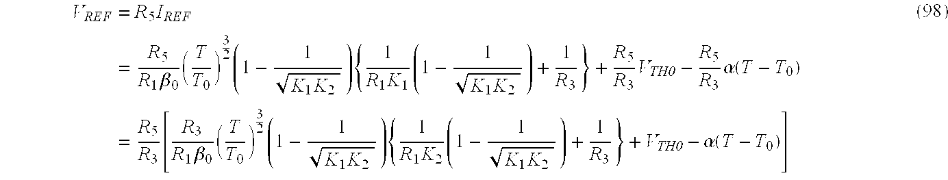


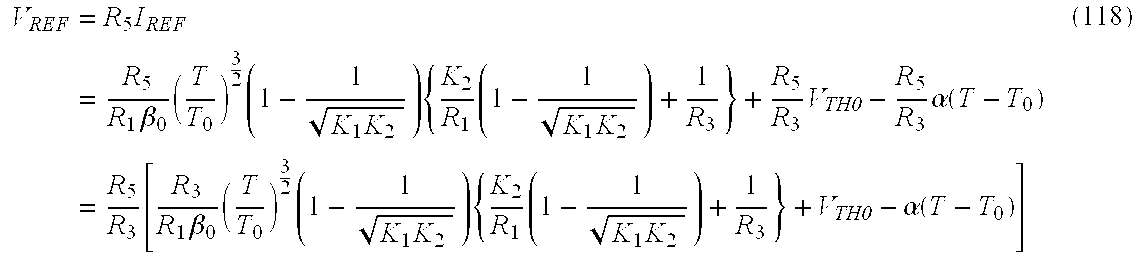


Claims (21)
Applications Claiming Priority (3)
| Application Number | Priority Date | Filing Date | Title |
|---|---|---|---|
| JP036139/2001 | 2001-02-13 | ||
| JP2001036139A JP3638530B2 (en) | 2001-02-13 | 2001-02-13 | Reference current circuit and reference voltage circuit |
| JP2001-036139 | 2001-02-13 |
Publications (2)
| Publication Number | Publication Date |
|---|---|
| US20020158614A1 US20020158614A1 (en) | 2002-10-31 |
| US6528979B2 true US6528979B2 (en) | 2003-03-04 |
Family
ID=18899459
Family Applications (1)
| Application Number | Title | Priority Date | Filing Date |
|---|---|---|---|
| US10/071,022 Expired - Lifetime US6528979B2 (en) | 2001-02-13 | 2002-02-08 | Reference current circuit and reference voltage circuit |
Country Status (4)
| Country | Link |
|---|---|
| US (1) | US6528979B2 (en) |
| EP (1) | EP1235132B1 (en) |
| JP (1) | JP3638530B2 (en) |
| DE (1) | DE60214452T2 (en) |
Cited By (22)
| Publication number | Priority date | Publication date | Assignee | Title |
|---|---|---|---|---|
| US20030107360A1 (en) * | 2001-12-06 | 2003-06-12 | Ionel Gheorghe | Low power bandgap circuit |
| US20030132796A1 (en) * | 2001-11-26 | 2003-07-17 | Stmicroelectronics S.A. | Temperature-compensated current source |
| US20040113682A1 (en) * | 2002-12-11 | 2004-06-17 | Hoon Siew Kuok | Threshold voltage extraction circuit |
| US20050001671A1 (en) * | 2003-06-19 | 2005-01-06 | Rohm Co., Ltd. | Constant voltage generator and electronic equipment using the same |
| US20050093530A1 (en) * | 2003-10-31 | 2005-05-05 | Jong-Chern Lee | Reference voltage generator |
| US20050264346A1 (en) * | 2004-05-06 | 2005-12-01 | Hack-Soo Oh | Generator for supplying reference voltage and reference current of stable level regardless of temperature variation |
| US20060044883A1 (en) * | 2004-09-01 | 2006-03-02 | Yangsung Joo | Low supply voltage temperature compensated reference voltage generator and method |
| US20060132223A1 (en) * | 2004-12-22 | 2006-06-22 | Cherek Brian J | Temperature-stable voltage reference circuit |
| US7193454B1 (en) * | 2004-07-08 | 2007-03-20 | Analog Devices, Inc. | Method and a circuit for producing a PTAT voltage, and a method and a circuit for producing a bandgap voltage reference |
| US20080088361A1 (en) * | 2006-10-16 | 2008-04-17 | Nec Electronics Corporation | Reference voltage generating circuit |
| US7394308B1 (en) * | 2003-03-07 | 2008-07-01 | Cypress Semiconductor Corp. | Circuit and method for implementing a low supply voltage current reference |
| US20080157820A1 (en) * | 2006-12-28 | 2008-07-03 | Roy Alan Hastings | Apparatus to compare an input voltage with a threshold voltage |
| US20080164567A1 (en) * | 2007-01-09 | 2008-07-10 | Motorola, Inc. | Band gap reference supply using nanotubes |
| US20090256628A1 (en) * | 2008-04-10 | 2009-10-15 | Nikolay Ilkov | Reference Current Circuit and Low Power Bias Circuit Using the Same |
| US20090289682A1 (en) * | 2008-03-06 | 2009-11-26 | Nikolay Ilkov | Potential Converter Circuit |
| US20090302823A1 (en) * | 2008-06-10 | 2009-12-10 | Analog Devices, Inc. | Voltage regulator circuit |
| US8082796B1 (en) * | 2008-01-28 | 2011-12-27 | Silicon Microstructures, Inc. | Temperature extraction from a pressure sensor |
| RU2519270C1 (en) * | 2012-10-25 | 2014-06-10 | Федеральное государственное бюджетное образовательное учреждение высшего профессионального образования "Южно-Российский государственный университет экономики и сервиса" (ФГБОУ ВПО "ЮРГУЭС") | Source of reference voltage |
| RU2520415C1 (en) * | 2012-12-29 | 2014-06-27 | Федеральное государственное бюджетное образовательное учреждение высшего профессионального образования "Южно-Российский государственный университет экономики и сервиса" (ФГБОУ ВПО "ЮРГУЭС") | Source of reference voltage |
| US20170077872A1 (en) * | 2015-09-16 | 2017-03-16 | Freescale Semiconductor, Inc. | Low power circuit for amplifying a voltage without using resistors |
| US10139849B2 (en) * | 2017-04-25 | 2018-11-27 | Honeywell International Inc. | Simple CMOS threshold voltage extraction circuit |
| US11353903B1 (en) * | 2021-03-31 | 2022-06-07 | Silicon Laboratories Inc. | Voltage reference circuit |
Families Citing this family (17)
| Publication number | Priority date | Publication date | Assignee | Title |
|---|---|---|---|---|
| JP2005063026A (en) * | 2003-08-08 | 2005-03-10 | Nec Micro Systems Ltd | Reference voltage generation circuit |
| KR100582742B1 (en) | 2004-12-21 | 2006-05-22 | 인티그런트 테크놀로지즈(주) | Circuit for generating reference current |
| JP4780968B2 (en) * | 2005-01-25 | 2011-09-28 | ルネサスエレクトロニクス株式会社 | Reference voltage circuit |
| JP4721726B2 (en) | 2005-02-25 | 2011-07-13 | 富士通セミコンダクター株式会社 | Differential amplifier |
| JP2007200234A (en) * | 2006-01-30 | 2007-08-09 | Nec Electronics Corp | Reference voltage circuit driven by nonlinear current mirror circuit |
| JP4658838B2 (en) * | 2006-03-17 | 2011-03-23 | Okiセミコンダクタ株式会社 | Reference potential generator |
| US9383089B2 (en) | 2008-06-24 | 2016-07-05 | Hongwu Yang | Heat radiation device for a lighting device |
| KR101015543B1 (en) | 2009-06-29 | 2011-02-16 | 광운대학교 산학협력단 | Reference voltage generator circuit |
| JP5424750B2 (en) * | 2009-07-09 | 2014-02-26 | 新日本無線株式会社 | Bias circuit |
| JP5706674B2 (en) * | 2010-11-24 | 2015-04-22 | セイコーインスツル株式会社 | Constant current circuit and reference voltage circuit |
| JP5782346B2 (en) * | 2011-09-27 | 2015-09-24 | セイコーインスツル株式会社 | Reference voltage circuit |
| JP6045148B2 (en) | 2011-12-15 | 2016-12-14 | エスアイアイ・セミコンダクタ株式会社 | Reference current generation circuit and reference voltage generation circuit |
| JP6600207B2 (en) * | 2015-09-17 | 2019-10-30 | ローム株式会社 | Reference current source circuit |
| FR3104344B1 (en) | 2019-12-06 | 2021-12-24 | Commissariat Energie Atomique | Electronic voltage divider circuit in FDSOI technology |
| JP2021189489A (en) * | 2020-05-25 | 2021-12-13 | 株式会社村田製作所 | Bias circuit |
| CN113050743B (en) * | 2021-03-25 | 2022-03-08 | 电子科技大学 | Current reference circuit capable of outputting multiple temperature coefficients |
| JP2022156360A (en) | 2021-03-31 | 2022-10-14 | ザインエレクトロニクス株式会社 | Standard current source |
Citations (16)
| Publication number | Priority date | Publication date | Assignee | Title |
|---|---|---|---|---|
| JPS59191629A (en) | 1983-04-15 | 1984-10-30 | Toshiba Corp | Constant current circuit |
| US4528496A (en) | 1983-06-23 | 1985-07-09 | National Semiconductor Corporation | Current supply for use in low voltage IC devices |
| EP0411657A1 (en) | 1989-08-03 | 1991-02-06 | Kabushiki Kaisha Toshiba | Constant voltage circuit |
| JPH07200086A (en) | 1993-12-28 | 1995-08-04 | Nec Corp | Reference current circuit and reference voltage circuit |
| US5440224A (en) | 1992-01-29 | 1995-08-08 | Nec Corporation | Reference voltage generating circuit formed of bipolar transistors |
| US5512817A (en) * | 1993-12-29 | 1996-04-30 | At&T Corp. | Bandgap voltage reference generator |
| US5570008A (en) * | 1993-04-14 | 1996-10-29 | Texas Instruments Deutschland Gmbh | Band gap reference voltage source |
| US5627461A (en) | 1993-12-08 | 1997-05-06 | Nec Corporation | Reference current circuit capable of preventing occurrence of a difference collector current which is caused by early voltage effect |
| US5783936A (en) * | 1995-06-12 | 1998-07-21 | International Business Machines Corporation | Temperature compensated reference current generator |
| US5910749A (en) | 1995-10-31 | 1999-06-08 | Nec Corporation | Current reference circuit with substantially no temperature dependence |
| US5926062A (en) | 1997-06-23 | 1999-07-20 | Nec Corporation | Reference voltage generating circuit |
| US5942888A (en) | 1996-05-07 | 1999-08-24 | Telefonaktiebolaget Lm Ericsson | Method and device for temperature dependent current generation |
| US6002244A (en) * | 1998-11-17 | 1999-12-14 | Impala Linear Corporation | Temperature monitoring circuit with thermal hysteresis |
| US6097179A (en) * | 1999-03-08 | 2000-08-01 | Texas Instruments Incorporated | Temperature compensating compact voltage regulator for integrated circuit device |
| US6181121B1 (en) * | 1999-03-04 | 2001-01-30 | Cypress Semiconductor Corp. | Low supply voltage BICMOS self-biased bandgap reference using a current summing architecture |
| US6351111B1 (en) * | 2001-04-13 | 2002-02-26 | Ami Semiconductor, Inc. | Circuits and methods for providing a current reference with a controlled temperature coefficient using a series composite resistor |
-
2001
- 2001-02-13 JP JP2001036139A patent/JP3638530B2/en not_active Expired - Fee Related
-
2002
- 2002-02-08 US US10/071,022 patent/US6528979B2/en not_active Expired - Lifetime
- 2002-02-13 EP EP02090058A patent/EP1235132B1/en not_active Expired - Lifetime
- 2002-02-13 DE DE60214452T patent/DE60214452T2/en not_active Expired - Fee Related
Patent Citations (16)
| Publication number | Priority date | Publication date | Assignee | Title |
|---|---|---|---|---|
| JPS59191629A (en) | 1983-04-15 | 1984-10-30 | Toshiba Corp | Constant current circuit |
| US4528496A (en) | 1983-06-23 | 1985-07-09 | National Semiconductor Corporation | Current supply for use in low voltage IC devices |
| EP0411657A1 (en) | 1989-08-03 | 1991-02-06 | Kabushiki Kaisha Toshiba | Constant voltage circuit |
| US5440224A (en) | 1992-01-29 | 1995-08-08 | Nec Corporation | Reference voltage generating circuit formed of bipolar transistors |
| US5570008A (en) * | 1993-04-14 | 1996-10-29 | Texas Instruments Deutschland Gmbh | Band gap reference voltage source |
| US5627461A (en) | 1993-12-08 | 1997-05-06 | Nec Corporation | Reference current circuit capable of preventing occurrence of a difference collector current which is caused by early voltage effect |
| JPH07200086A (en) | 1993-12-28 | 1995-08-04 | Nec Corp | Reference current circuit and reference voltage circuit |
| US5512817A (en) * | 1993-12-29 | 1996-04-30 | At&T Corp. | Bandgap voltage reference generator |
| US5783936A (en) * | 1995-06-12 | 1998-07-21 | International Business Machines Corporation | Temperature compensated reference current generator |
| US5910749A (en) | 1995-10-31 | 1999-06-08 | Nec Corporation | Current reference circuit with substantially no temperature dependence |
| US5942888A (en) | 1996-05-07 | 1999-08-24 | Telefonaktiebolaget Lm Ericsson | Method and device for temperature dependent current generation |
| US5926062A (en) | 1997-06-23 | 1999-07-20 | Nec Corporation | Reference voltage generating circuit |
| US6002244A (en) * | 1998-11-17 | 1999-12-14 | Impala Linear Corporation | Temperature monitoring circuit with thermal hysteresis |
| US6181121B1 (en) * | 1999-03-04 | 2001-01-30 | Cypress Semiconductor Corp. | Low supply voltage BICMOS self-biased bandgap reference using a current summing architecture |
| US6097179A (en) * | 1999-03-08 | 2000-08-01 | Texas Instruments Incorporated | Temperature compensating compact voltage regulator for integrated circuit device |
| US6351111B1 (en) * | 2001-04-13 | 2002-02-26 | Ami Semiconductor, Inc. | Circuits and methods for providing a current reference with a controlled temperature coefficient using a series composite resistor |
Non-Patent Citations (1)
| Title |
|---|
| Neuteboom, Harry and Ben M.J. Kup and Mark Janssens, "A DSP-Based Hearing Instrument IC". IEEE Journal of Solid-State Circuits, vol. 32, No. 11, Nov. 1997, pp. 1790-1806. |
Cited By (43)
| Publication number | Priority date | Publication date | Assignee | Title |
|---|---|---|---|---|
| US20030132796A1 (en) * | 2001-11-26 | 2003-07-17 | Stmicroelectronics S.A. | Temperature-compensated current source |
| US6759893B2 (en) * | 2001-11-26 | 2004-07-06 | Stmicroelectronics Sa | Temperature-compensated current source |
| US6788041B2 (en) * | 2001-12-06 | 2004-09-07 | Skyworks Solutions Inc | Low power bandgap circuit |
| WO2003050847A3 (en) * | 2001-12-06 | 2004-02-05 | Skyworks Solutions Inc | Low power bandgap circuit |
| WO2003050847A2 (en) * | 2001-12-06 | 2003-06-19 | Skyworks Solutions, Inc. | Low power bandgap circuit |
| US20030107360A1 (en) * | 2001-12-06 | 2003-06-12 | Ionel Gheorghe | Low power bandgap circuit |
| US20040113682A1 (en) * | 2002-12-11 | 2004-06-17 | Hoon Siew Kuok | Threshold voltage extraction circuit |
| US6844772B2 (en) * | 2002-12-11 | 2005-01-18 | Texas Instruments Incorporated | Threshold voltage extraction circuit |
| US7394308B1 (en) * | 2003-03-07 | 2008-07-01 | Cypress Semiconductor Corp. | Circuit and method for implementing a low supply voltage current reference |
| US7151365B2 (en) | 2003-06-19 | 2006-12-19 | Rohm Co., Ltd. | Constant voltage generator and electronic equipment using the same |
| US20050001671A1 (en) * | 2003-06-19 | 2005-01-06 | Rohm Co., Ltd. | Constant voltage generator and electronic equipment using the same |
| US7023181B2 (en) * | 2003-06-19 | 2006-04-04 | Rohm Co., Ltd. | Constant voltage generator and electronic equipment using the same |
| US20060125461A1 (en) * | 2003-06-19 | 2006-06-15 | Rohm Co., Ltd. | Constant voltage generator and electronic equipment using the same |
| US20050093530A1 (en) * | 2003-10-31 | 2005-05-05 | Jong-Chern Lee | Reference voltage generator |
| US7157893B2 (en) * | 2003-10-31 | 2007-01-02 | Hynix Semiconductor Inc. | Temperature independent reference voltage generator |
| US20050264346A1 (en) * | 2004-05-06 | 2005-12-01 | Hack-Soo Oh | Generator for supplying reference voltage and reference current of stable level regardless of temperature variation |
| US7233195B2 (en) * | 2004-05-06 | 2007-06-19 | Magnachip Semiconductor, Ltd. | Generator for supplying reference voltage and reference current of stable level regardless of temperature variation |
| US7193454B1 (en) * | 2004-07-08 | 2007-03-20 | Analog Devices, Inc. | Method and a circuit for producing a PTAT voltage, and a method and a circuit for producing a bandgap voltage reference |
| US7116588B2 (en) | 2004-09-01 | 2006-10-03 | Micron Technology, Inc. | Low supply voltage temperature compensated reference voltage generator and method |
| US20060203572A1 (en) * | 2004-09-01 | 2006-09-14 | Yangsung Joo | Low supply voltage temperature compensated reference voltage generator and method |
| US20060044883A1 (en) * | 2004-09-01 | 2006-03-02 | Yangsung Joo | Low supply voltage temperature compensated reference voltage generator and method |
| US7313034B2 (en) * | 2004-09-01 | 2007-12-25 | Micron Technology, Inc. | Low supply voltage temperature compensated reference voltage generator and method |
| WO2006069157A2 (en) * | 2004-12-22 | 2006-06-29 | Atmel Corporation | Temperature-stable voltage reference circuit |
| US20060132223A1 (en) * | 2004-12-22 | 2006-06-22 | Cherek Brian J | Temperature-stable voltage reference circuit |
| WO2006069157A3 (en) * | 2004-12-22 | 2006-10-05 | Atmel Corp | Temperature-stable voltage reference circuit |
| US20080088361A1 (en) * | 2006-10-16 | 2008-04-17 | Nec Electronics Corporation | Reference voltage generating circuit |
| US20080129272A1 (en) * | 2006-10-16 | 2008-06-05 | Nec Electronics Corporation | Reference voltage generating circuit |
| US7592859B2 (en) * | 2006-12-28 | 2009-09-22 | Texas Instruments Incorporated | Apparatus to compare an input voltage with a threshold voltage |
| US20080157820A1 (en) * | 2006-12-28 | 2008-07-03 | Roy Alan Hastings | Apparatus to compare an input voltage with a threshold voltage |
| US20080164567A1 (en) * | 2007-01-09 | 2008-07-10 | Motorola, Inc. | Band gap reference supply using nanotubes |
| US8082796B1 (en) * | 2008-01-28 | 2011-12-27 | Silicon Microstructures, Inc. | Temperature extraction from a pressure sensor |
| US20090289682A1 (en) * | 2008-03-06 | 2009-11-26 | Nikolay Ilkov | Potential Converter Circuit |
| US7932753B2 (en) * | 2008-03-06 | 2011-04-26 | Infineon Technologies Ag | Potential converter circuit |
| US20090256628A1 (en) * | 2008-04-10 | 2009-10-15 | Nikolay Ilkov | Reference Current Circuit and Low Power Bias Circuit Using the Same |
| US7750721B2 (en) | 2008-04-10 | 2010-07-06 | Infineon Technologies Ag | Reference current circuit and low power bias circuit using the same |
| US8159206B2 (en) * | 2008-06-10 | 2012-04-17 | Analog Devices, Inc. | Voltage reference circuit based on 3-transistor bandgap cell |
| US20090302823A1 (en) * | 2008-06-10 | 2009-12-10 | Analog Devices, Inc. | Voltage regulator circuit |
| RU2519270C1 (en) * | 2012-10-25 | 2014-06-10 | Федеральное государственное бюджетное образовательное учреждение высшего профессионального образования "Южно-Российский государственный университет экономики и сервиса" (ФГБОУ ВПО "ЮРГУЭС") | Source of reference voltage |
| RU2520415C1 (en) * | 2012-12-29 | 2014-06-27 | Федеральное государственное бюджетное образовательное учреждение высшего профессионального образования "Южно-Российский государственный университет экономики и сервиса" (ФГБОУ ВПО "ЮРГУЭС") | Source of reference voltage |
| US20170077872A1 (en) * | 2015-09-16 | 2017-03-16 | Freescale Semiconductor, Inc. | Low power circuit for amplifying a voltage without using resistors |
| US9641129B2 (en) * | 2015-09-16 | 2017-05-02 | Nxp Usa, Inc. | Low power circuit for amplifying a voltage without using resistors |
| US10139849B2 (en) * | 2017-04-25 | 2018-11-27 | Honeywell International Inc. | Simple CMOS threshold voltage extraction circuit |
| US11353903B1 (en) * | 2021-03-31 | 2022-06-07 | Silicon Laboratories Inc. | Voltage reference circuit |
Also Published As
| Publication number | Publication date |
|---|---|
| EP1235132A2 (en) | 2002-08-28 |
| DE60214452D1 (en) | 2006-10-19 |
| EP1235132A3 (en) | 2002-10-02 |
| JP2002244748A (en) | 2002-08-30 |
| EP1235132B1 (en) | 2006-09-06 |
| JP3638530B2 (en) | 2005-04-13 |
| US20020158614A1 (en) | 2002-10-31 |
| DE60214452T2 (en) | 2007-09-13 |
Similar Documents
| Publication | Publication Date | Title |
|---|---|---|
| US6528979B2 (en) | Reference current circuit and reference voltage circuit | |
| US10599176B1 (en) | Bandgap reference circuit and high-order temperature compensation method | |
| US7088085B2 (en) | CMOS bandgap current and voltage generator | |
| US7622906B2 (en) | Reference voltage generation circuit responsive to ambient temperature | |
| US7511568B2 (en) | Reference voltage circuit | |
| JP3586073B2 (en) | Reference voltage generation circuit | |
| US7170336B2 (en) | Low voltage bandgap reference (BGR) circuit | |
| US8159206B2 (en) | Voltage reference circuit based on 3-transistor bandgap cell | |
| US7511566B2 (en) | Semiconductor circuit with positive temperature dependence resistor | |
| US7274250B2 (en) | Low-voltage, buffered bandgap reference with selectable output voltage | |
| US7633333B2 (en) | Systems, apparatus and methods relating to bandgap circuits | |
| US7808305B2 (en) | Low-voltage band-gap reference voltage bias circuit | |
| US20110121809A1 (en) | Voltage reference circuit | |
| US11092991B2 (en) | System and method for voltage generation | |
| US9122290B2 (en) | Bandgap reference circuit | |
| US8816756B1 (en) | Bandgap reference circuit | |
| US6150871A (en) | Low power voltage reference with improved line regulation | |
| JPH08123568A (en) | Reference current circuit | |
| US10379567B2 (en) | Bandgap reference circuitry | |
| US20040169549A1 (en) | Bandgap reference circuit | |
| US6184745B1 (en) | Reference voltage generating circuit | |
| US20110169551A1 (en) | Temperature sensor and method | |
| US20020109491A1 (en) | Regulated voltage generator for integrated circuit | |
| US20080094050A1 (en) | Reference current generator circuit | |
| US20020109490A1 (en) | Reference current source having MOS transistors |
Legal Events
| Date | Code | Title | Description |
|---|---|---|---|
| AS | Assignment |
Owner name: NEC CORPORATION, JAPAN Free format text: ASSIGNMENT OF ASSIGNORS INTEREST;ASSIGNOR:KIMURA, KATSUJI;REEL/FRAME:012575/0052 Effective date: 20020204 |
|
| STCF | Information on status: patent grant |
Free format text: PATENTED CASE |
|
| AS | Assignment |
Owner name: NEC ELECTRONICS CORPORATION, JAPAN Free format text: ASSIGNMENT OF ASSIGNORS INTEREST;ASSIGNOR:NEC CORPORATION;REEL/FRAME:013736/0321 Effective date: 20021101 |
|
| FPAY | Fee payment |
Year of fee payment: 4 |
|
| FPAY | Fee payment |
Year of fee payment: 8 |
|
| AS | Assignment |
Owner name: RENESAS ELECTRONICS CORPORATION, JAPAN Free format text: CHANGE OF NAME;ASSIGNOR:NEC ELECTRONICS CORPORATION;REEL/FRAME:025486/0530 Effective date: 20100401 |
|
| FPAY | Fee payment |
Year of fee payment: 12 |
|
| AS | Assignment |
Owner name: RENESAS ELECTRONICS CORPORATION, JAPAN Free format text: CHANGE OF ADDRESS;ASSIGNOR:RENESAS ELECTRONICS CORPORATION;REEL/FRAME:044928/0001 Effective date: 20150806 |