US6597562B1 - Electrically polar integrated capacitor and method of making same - Google Patents
Electrically polar integrated capacitor and method of making same Download PDFInfo
- Publication number
- US6597562B1 US6597562B1 US10/065,043 US6504302A US6597562B1 US 6597562 B1 US6597562 B1 US 6597562B1 US 6504302 A US6504302 A US 6504302A US 6597562 B1 US6597562 B1 US 6597562B1
- Authority
- US
- United States
- Prior art keywords
- capacitor
- vertical
- plate
- semiconductor substrate
- node
- Prior art date
- Legal status (The legal status is an assumption and is not a legal conclusion. Google has not performed a legal analysis and makes no representation as to the accuracy of the status listed.)
- Expired - Lifetime
Links
Images


Classifications
-
- H—ELECTRICITY
- H01—ELECTRIC ELEMENTS
- H01L—SEMICONDUCTOR DEVICES NOT COVERED BY CLASS H10
- H01L28/00—Passive two-terminal components without a potential-jump or surface barrier for integrated circuits; Details thereof; Multistep manufacturing processes therefor
- H01L28/40—Capacitors
- H01L28/60—Electrodes
- H01L28/82—Electrodes with an enlarged surface, e.g. formed by texturisation
-
- H—ELECTRICITY
- H01—ELECTRIC ELEMENTS
- H01L—SEMICONDUCTOR DEVICES NOT COVERED BY CLASS H10
- H01L23/00—Details of semiconductor or other solid state devices
- H01L23/52—Arrangements for conducting electric current within the device in operation from one component to another, i.e. interconnections, e.g. wires, lead frames
- H01L23/522—Arrangements for conducting electric current within the device in operation from one component to another, i.e. interconnections, e.g. wires, lead frames including external interconnections consisting of a multilayer structure of conductive and insulating layers inseparably formed on the semiconductor body
- H01L23/5222—Capacitive arrangements or effects of, or between wiring layers
- H01L23/5223—Capacitor integral with wiring layers
-
- H—ELECTRICITY
- H01—ELECTRIC ELEMENTS
- H01L—SEMICONDUCTOR DEVICES NOT COVERED BY CLASS H10
- H01L23/00—Details of semiconductor or other solid state devices
- H01L23/52—Arrangements for conducting electric current within the device in operation from one component to another, i.e. interconnections, e.g. wires, lead frames
- H01L23/522—Arrangements for conducting electric current within the device in operation from one component to another, i.e. interconnections, e.g. wires, lead frames including external interconnections consisting of a multilayer structure of conductive and insulating layers inseparably formed on the semiconductor body
- H01L23/5222—Capacitive arrangements or effects of, or between wiring layers
- H01L23/5225—Shielding layers formed together with wiring layers
-
- H—ELECTRICITY
- H01—ELECTRIC ELEMENTS
- H01L—SEMICONDUCTOR DEVICES NOT COVERED BY CLASS H10
- H01L2924/00—Indexing scheme for arrangements or methods for connecting or disconnecting semiconductor or solid-state bodies as covered by H01L24/00
- H01L2924/0001—Technical content checked by a classifier
- H01L2924/0002—Not covered by any one of groups H01L24/00, H01L24/00 and H01L2224/00
Definitions
- the present invention relates to an integrated capacitor, and more particularly, to an electrically polar integrated capacitor suited for analog/digital(A/D) converters, digital/analog(D/A) converters, or switch cap circuits.
- Passive components such as capacitors are extensively used in integrated circuit (IC) design for radio-frequency (RF) and mixed-signal applications, such as filters, resonant circuits and bypassing. Due to trends toward higher-levels of integration to achieve reduction in cost associated with IC fabrication processes, the IC industry continually strives to economize each step of the fabrication process to the greatest extent possible.
- IC integrated circuit
- RF radio-frequency
- mixed-signal applications such as filters, resonant circuits and bypassing. Due to trends toward higher-levels of integration to achieve reduction in cost associated with IC fabrication processes, the IC industry continually strives to economize each step of the fabrication process to the greatest extent possible.
- FIG. 1 is a typical view fragmentarily illustrating a high capacitance density integrated capacitor according to the prior art.
- the prior art integrated capacitor 1 consists of a plurality of parallel-arranged vertical metal plates 100 and 120 .
- different shadings are used to distinguish the two terminals of the capacitor 1 , where the vertical plates 120 are electrically connected to terminal A (or node A), and the vertical plates 100 are electrically connected to terminal B (or node B).
- the vertical metal plates 100 and 120 are fabricated on a semiconductor substrate (not explicitly shown).
- Each of the vertical metal plates 100 consists of a plurality of metal slabs 10 a, 10 b, 10 c and 10 d connected vertically using multiple via plugs 11 a, 11 b and 11 c that are typically composed of metals.
- Each of the vertical metal plates 120 consists of a plurality of metal slabs 12 a, 12 b, 12 c and 12 d connected vertically using multiple via plugs 13 a, 13 b and 13 c.
- the vertical plate 100 and the vertical plate 120 are isolated from each other by a dielectric layer (not shown).
- metal slabs 10 a, 10 b, 10 c and 10 d and metal slabs 12 a, 12 b, 12 c and 12 d of the prior art integrated capacitor 1 are fabricated in an interconnect process known in the art. Unlike the traditional metal-on-metal (MOM) capacitors as known to those skilled in the art, the prior art integrated capacitor 1 is fabricated without using extra photo-masks, thereby reducing production cost. Moreover, the prior art integrated capacitor 1 provides higher capacitance per unit area.
- MOM metal-on-metal
- FIG. 2 is an equivalent circuit diagram of the prior art integrated capacitor 1 as set forth in FIG. 1 .
- the vertical plates 120 of the integrated capacitor 1 are electrically connected to the node A
- the vertical plates 100 of the integrated capacitor 1 are electrically connected to the node B.
- inter-plate capacitance C in , parasitic capacitance C A , and parasitic capacitance C B are generated between node A and node B.
- the parasitic capacitance C A is induced between lowest metal slab 10 a of the vertical metal plate 100 and the electrically grounded semiconductor substrate.
- the parasitic capacitance C B is induced between lowest metal slab 12 a of the vertical metal plate 120 and the electrically grounded semiconductor substrate. Due to the non-polar property presented by the prior art integrated capacitor 1 , the prior art integrated capacitor 1 is therefore not suited for the design of analog/digital(A/D) converters, digital/analog (D/A) converters, or switch cap circuits.
- the primary objective of the claimed invention is to provide an electrically polar integrated capacitor with a high capacitance density that is suited for analog/digital(A/D) converters, digital/analog(D/A) converters, or switch cap circuits.
- an integrated capacitor having an electrically polar property comprises a semiconductor substrate.
- a first vertical plate is laid over the semiconductor substrate.
- the first vertical plate consists of a plurality of first conductive slabs connected vertically using multiple first via plugs.
- a second vertical plate is laid over the semiconductor substrate in parallel with the first vertical plate.
- the second vertical plate consists of a plurality of second conductive slabs connected vertically using multiple second via plugs.
- a conductive plate is laid under the first vertical plate and second vertical plate over the semiconductor substrate for shielding the first vertical plate from producing a plate-to-substrate parasitic capacitance thereof.
- the second vertical plate is electrically connected with the conductive plate using a third via plug.
- an integrated capacitor having an electrically polar property comprises a semiconductor substrate and a first vertical capacitor bar laid over the semiconductor substrate.
- the first vertical capacitor bar consists of a plurality of first conductive squares connected vertically using multiple first via plugs.
- a second vertical capacitor bar is laid over the semiconductor substrate in parallel with the first vertical capacitor bar.
- the second vertical capacitor bar consists of a plurality of second conductive squares connected vertically using multiple second via plugs.
- a parallel conductive plate is laid under the first vertical capacitor bar and second vertical capacitor bar over the semiconductor substrate for shielding the first vertical capacitor bar from producing a plate-to-substrate parasitic capacitance thereof.
- the second vertical capacitor bar is electrically connected with the parallel conductive plate using a third via plug.
- FIG. 1 is an enlarged typical view fragmentarily illustrating a high-density integrated capacitor structure according to the prior art.
- FIG. 2 is an equivalent circuit diagram of the prior art integrated capacitor as set forth in FIG. 1 .
- FIG. 3 is an enlarged perspective view fragmentarily illustrating a high capacitance density integrated capacitor according to the present invention.
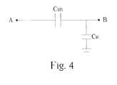
- FIG. 4 is an equivalent circuit diagram of the integrated capacitor as set forth in FIG. 3 .
- FIG. 5 is a perspective view of the integrated capacitor structure according to another preferred embodiment of this invention.
- FIG. 3 is a perspective view fragmentarily illustrating a high capacitance density integrated capacitor according to the present invention.
- the integrated capacitor 3 consists of a plurality of parallel-arranged vertical metal plates 300 and 320 .
- different shadings are used to distinguish the two terminals of the capacitor 3 , where the vertical plates 320 are electrically connected to terminal A (or node A), and the vertical plates 300 are electrically connected to terminal B (or node B).
- the vertical metal plates 300 and 320 are fabricated on a semiconductor substrate (not explicitly shown).
- Each of the vertical metal plates 300 consists of a plurality of metal slabs 30 a, 30 b, 30 c and 30 d connected vertically using multiple via plugs 31 a, 31 b and 31 c that are typically composed of metals.
- Each of the vertical metal plates 320 consists of a plurality of metal slabs 32 a, 32 b, 32 c and 32 d connected vertically using multiple via plugs 33 a, 33 b and 33 c.
- the vertical plate 300 and the vertical plate 320 are isolated from each other by a dielectric layer (not shown).
- metal slabs 30 a, 30 b, 30 c and 30 d and metal slabs 32 a, 32 b, 32 c and 32 d of the integrated capacitor 3 are fabricated in an interconnect process known in the art. Since the integrated capacitor 3 is fabricated without using extra photo-masks, production cost is reduced.
- the integrated capacitor 3 of this invention further comprises a parallel conductive plate 340 laid between the underlying semiconductor substrate (not explicitly shown) and the overlying integrated vertical metal plates 300 and 320 .
- the parallel conductive plate 340 is electrically connected with the vertical metal plates 300 using a via plug 340 a.
- the parallel conductive plate 340 is electrically isolated from the vertical metal plates 320 using a dielectric layer (not shown).
- the parallel conductive plate 340 is made of conductive materials such as metals or polysilicon. According to the preferred embodiment of the present invention, the conductive plate 340 is defined with the first layer metal (metal 1 ) in the interconnection process of the integrated circuit.
- FIG. 4 is an equivalent circuit diagram of the integrated capacitor 3 as set forth in FIG. 3 .
- the vertical plates 320 of the integrated capacitor 3 are electrically connected to the node A, and the vertical plates 300 of the integrated capacitor 3 are electrically connected to the node B.
- inter-plate capacitance C in and parasitic capacitance C B are generated between node A and node B.
- the parasitic capacitance C B is induced between the vertical metal plate 320 and the electrically grounded semiconductor substrate. It is noteworthy that there is no parasitic capacitance produced at node A due to the shielding of the parallel conductive plate 340 . Since the integrated capacitor 3 has a polar property, it is suited for the design of analog/digital(A/D) converters, digital/analog(D/A) converters, or switch cap circuits.
- FIG. 5 is a perspective view of the capacitor structure according to another preferred embodiment of this invention.
- the integrated capacitor 5 consists of a plurality of parallel-arranged vertical capacitor bars or electrode bars 500 and 520 .
- different shadings are used to distinguish the two terminals of the capacitor 5 , where the vertical capacitor bars 520 are electrically connected to terminal A (or node A), and the vertical capacitor bars 500 are electrically connected to terminal B (or node B).
- the vertical capacitor bars 500 and 520 are fabricated on a semiconductor substrate (not explicitly shown).
- Each of the vertical capacitor bars 500 consists of a plurality of metal squares 50 a, 50 b, 50 c and 50 d connected vertically using multiple via plugs 51 a, 51 b and 51 c that are typically composed of metals.
- Each of the vertical capacitor bars 520 consists of a plurality of metal slabs 52 a, 52 b, 52 c and 52 d connected vertically using multiple via plugs.
- the vertical plate 500 and the vertical plate 520 are isolated from each other by a dielectric layer (not shown).
- metal squares 50 a, 50 b, 50 c and 50 d and metal squares 52 a, 52 b, 52 c and 52 d of the integrated capacitor 5 are fabricated in an interconnect process known in the art. Since the integrated capacitor 5 is fabricated without using extra photo-masks, production cost is reduced.
- the integrated capacitor 5 further comprises a parallel conductive plate 540 laid between the underlying semiconductor substrate (not explicitly shown) and the overlying integrated vertical capacitor bars 500 and 520 .
- the parallel conductive plate 540 is electrically connected with the vertical capacitor bars 500 using a via plug 540 a.
- the parallel conductive plate 540 is electrically isolated from the vertical capacitor bars 520 using a dielectric layer (not shown).
- the parallel conductive plate 540 is made of conductive materials such as metals or polysilicon. According to the preferred embodiment of the present invention, the conductive plate 540 is defined with the first layer metal (metal 1 ) in the interconnection process of the integrated circuit.
- this invention also discloses a method of forming an integrated capacitor.
- the method comprises the following steps:
Abstract
Description
Claims (20)
Applications Claiming Priority (2)
| Application Number | Priority Date | Filing Date | Title |
|---|---|---|---|
| TW091115471A TW541646B (en) | 2002-07-11 | 2002-07-11 | Polar integrated capacitor and method of making same |
| TW091115471 | 2002-07-11 |
Publications (1)
| Publication Number | Publication Date |
|---|---|
| US6597562B1 true US6597562B1 (en) | 2003-07-22 |
Family
ID=21688317
Family Applications (1)
| Application Number | Title | Priority Date | Filing Date |
|---|---|---|---|
| US10/065,043 Expired - Lifetime US6597562B1 (en) | 2002-07-11 | 2002-09-13 | Electrically polar integrated capacitor and method of making same |
Country Status (2)
| Country | Link |
|---|---|
| US (1) | US6597562B1 (en) |
| TW (1) | TW541646B (en) |
Cited By (26)
| Publication number | Priority date | Publication date | Assignee | Title |
|---|---|---|---|---|
| US6784050B1 (en) | 2000-09-05 | 2004-08-31 | Marvell International Ltd. | Fringing capacitor structure |
| US20050063137A1 (en) * | 2003-09-24 | 2005-03-24 | Intel Corporation | Vertical capacitor apparatus, systems, and methods |
| US6974744B1 (en) | 2000-09-05 | 2005-12-13 | Marvell International Ltd. | Fringing capacitor structure |
| US6980414B1 (en) | 2004-06-16 | 2005-12-27 | Marvell International, Ltd. | Capacitor structure in a semiconductor device |
| US20060181656A1 (en) * | 2005-02-15 | 2006-08-17 | Matsushita Electric Industrial Co., Ltd. | Placement configuration of MIM type capacitance element |
| US20070155112A1 (en) * | 2005-12-30 | 2007-07-05 | Chan Ho Park | Mom capacitor |
| US20070215928A1 (en) * | 2006-03-20 | 2007-09-20 | Standard Microsystems Corporation | Fringe capacitor using bootstrapped non-metal layer |
| US20080158776A1 (en) * | 2006-12-29 | 2008-07-03 | Industrial Technology Research Institute | Face-centered cubic structure capacitor and method of fabricating the same |
| US20080265369A1 (en) * | 2007-04-30 | 2008-10-30 | Taiwan Semiconductor Manufacturing Co., Ltd. | Semiconductor Capacitor Structure |
| US20100038752A1 (en) * | 2008-08-15 | 2010-02-18 | Chartered Semiconductor Manufacturing, Ltd. | Modular & scalable intra-metal capacitors |
| US20100127348A1 (en) * | 2008-11-21 | 2010-05-27 | Xilinx, Inc. | Integrated capicitor with cabled plates |
| US20100127309A1 (en) * | 2008-11-21 | 2010-05-27 | Xilinx, Inc. | Integrated capacitor with alternating layered segments |
| US20100127351A1 (en) * | 2008-11-21 | 2010-05-27 | Xilinx, Inc. | Integrated capacitor with interlinked lateral fins |
| US20100127349A1 (en) * | 2008-11-21 | 2010-05-27 | Xilinx, Inc. | Integrated capacitor with array of crosses |
| US20100127347A1 (en) * | 2008-11-21 | 2010-05-27 | Xilinx, Inc. | Shielding for integrated capacitors |
| US7994610B1 (en) | 2008-11-21 | 2011-08-09 | Xilinx, Inc. | Integrated capacitor with tartan cross section |
| US20130277803A1 (en) * | 2010-12-20 | 2013-10-24 | Stmicroelectronics S.R.L. | Connection structure for an integrated circuit with capacitive function |
| US8653844B2 (en) | 2011-03-07 | 2014-02-18 | Xilinx, Inc. | Calibrating device performance within an integrated circuit |
| US8941974B2 (en) | 2011-09-09 | 2015-01-27 | Xilinx, Inc. | Interdigitated capacitor having digits of varying width |
| US9270247B2 (en) | 2013-11-27 | 2016-02-23 | Xilinx, Inc. | High quality factor inductive and capacitive circuit structure |
| US20160118343A1 (en) * | 2014-10-27 | 2016-04-28 | Renesas Electronics Corporation | Semiconductor device |
| US9418788B2 (en) | 2014-03-16 | 2016-08-16 | Apple Inc. | Precision half cell for sub-FEMTO unit cap and capacitive DAC architecture in SAR ADC |
| US9524964B2 (en) | 2014-08-14 | 2016-12-20 | Xilinx, Inc. | Capacitor structure in an integrated circuit |
| US11355431B2 (en) * | 2020-10-07 | 2022-06-07 | United Microelectronics Corporation | Semiconductor structure |
| US20220285265A1 (en) * | 2019-06-14 | 2022-09-08 | Taiwan Semiconductor Manufacturing Company Ltd. | Integrated circuit structure of capacitive device |
| US11605503B2 (en) * | 2017-11-30 | 2023-03-14 | Murata Manufacturing Co., Ltd. | Front and back electrode trench capacitor |
Citations (4)
| Publication number | Priority date | Publication date | Assignee | Title |
|---|---|---|---|---|
| US5208725A (en) * | 1992-08-19 | 1993-05-04 | Akcasu Osman E | High capacitance structure in a semiconductor device |
| US6037621A (en) * | 1998-07-29 | 2000-03-14 | Lucent Technologies Inc. | On-chip capacitor structure |
| US6188121B1 (en) * | 1997-07-23 | 2001-02-13 | Sgs-Thomson Microelectronics S.R.L. | High voltage capacitor |
| US6385033B1 (en) * | 2000-09-29 | 2002-05-07 | Intel Corporation | Fingered capacitor in an integrated circuit |
-
2002
- 2002-07-11 TW TW091115471A patent/TW541646B/en not_active IP Right Cessation
- 2002-09-13 US US10/065,043 patent/US6597562B1/en not_active Expired - Lifetime
Patent Citations (4)
| Publication number | Priority date | Publication date | Assignee | Title |
|---|---|---|---|---|
| US5208725A (en) * | 1992-08-19 | 1993-05-04 | Akcasu Osman E | High capacitance structure in a semiconductor device |
| US6188121B1 (en) * | 1997-07-23 | 2001-02-13 | Sgs-Thomson Microelectronics S.R.L. | High voltage capacitor |
| US6037621A (en) * | 1998-07-29 | 2000-03-14 | Lucent Technologies Inc. | On-chip capacitor structure |
| US6385033B1 (en) * | 2000-09-29 | 2002-05-07 | Intel Corporation | Fingered capacitor in an integrated circuit |
Cited By (49)
| Publication number | Priority date | Publication date | Assignee | Title |
|---|---|---|---|---|
| US6885543B1 (en) | 2000-09-05 | 2005-04-26 | Marvell International, Ltd. | Fringing capacitor structure |
| US6974744B1 (en) | 2000-09-05 | 2005-12-13 | Marvell International Ltd. | Fringing capacitor structure |
| US6784050B1 (en) | 2000-09-05 | 2004-08-31 | Marvell International Ltd. | Fringing capacitor structure |
| US9017427B1 (en) | 2001-01-18 | 2015-04-28 | Marvell International Ltd. | Method of creating capacitor structure in a semiconductor device |
| US20050063137A1 (en) * | 2003-09-24 | 2005-03-24 | Intel Corporation | Vertical capacitor apparatus, systems, and methods |
| US6885544B2 (en) * | 2003-09-24 | 2005-04-26 | Intel Corporation | Vertical capacitor apparatus, systems, and methods |
| US7352557B2 (en) | 2003-09-24 | 2008-04-01 | Intel Corporation | Vertical capacitor apparatus, systems, and methods |
| US7578858B1 (en) | 2004-06-16 | 2009-08-25 | Marvell International Ltd. | Making capacitor structure in a semiconductor device |
| US6980414B1 (en) | 2004-06-16 | 2005-12-27 | Marvell International, Ltd. | Capacitor structure in a semiconductor device |
| US7116544B1 (en) | 2004-06-16 | 2006-10-03 | Marvell International, Ltd. | Capacitor structure in a semiconductor device |
| US8537524B1 (en) | 2004-06-16 | 2013-09-17 | Marvell International Ltd. | Capacitor structure in a semiconductor device |
| US7988744B1 (en) | 2004-06-16 | 2011-08-02 | Marvell International Ltd. | Method of producing capacitor structure in a semiconductor device |
| US20060181656A1 (en) * | 2005-02-15 | 2006-08-17 | Matsushita Electric Industrial Co., Ltd. | Placement configuration of MIM type capacitance element |
| US20080278885A1 (en) * | 2005-02-15 | 2008-11-13 | Matsushita Electric Industrial Co., Ltd. | Placement configuration of MIM type capacitance element |
| US7515394B2 (en) * | 2005-02-15 | 2009-04-07 | Panasonic Corporation | Placement configuration of MIM type capacitance element |
| US8179659B2 (en) | 2005-02-15 | 2012-05-15 | Panasonic Corporation | Placement configuration of MIM type capacitance element |
| US20070155112A1 (en) * | 2005-12-30 | 2007-07-05 | Chan Ho Park | Mom capacitor |
| US8076752B2 (en) * | 2006-03-20 | 2011-12-13 | Standard Microsystems Corporation | Fringe capacitor using bootstrapped non-metal layer |
| US20070215928A1 (en) * | 2006-03-20 | 2007-09-20 | Standard Microsystems Corporation | Fringe capacitor using bootstrapped non-metal layer |
| US8299575B2 (en) | 2006-03-20 | 2012-10-30 | Standard Microsystems Corporation | High-density capacitor configured on a semiconductor |
| US8299576B2 (en) | 2006-03-20 | 2012-10-30 | Standard Microsystems Corporation | Circuit with high-density capacitors using bootstrapped non-metal layer |
| US8299577B2 (en) | 2006-03-20 | 2012-10-30 | Standard Microsystems Corporation | Fringe capacitor using bootstrapped non-metal layer |
| US7564675B2 (en) * | 2006-12-29 | 2009-07-21 | Industrial Technology Research Institute | Face-centered cubic structure capacitor and method of fabricating the same |
| US20080158776A1 (en) * | 2006-12-29 | 2008-07-03 | Industrial Technology Research Institute | Face-centered cubic structure capacitor and method of fabricating the same |
| US20080265369A1 (en) * | 2007-04-30 | 2008-10-30 | Taiwan Semiconductor Manufacturing Co., Ltd. | Semiconductor Capacitor Structure |
| US9177908B2 (en) | 2007-04-30 | 2015-11-03 | Taiwan Semiconductor Manufacturing Company, Limited | Stacked semiconductor capacitor structure |
| US20100038752A1 (en) * | 2008-08-15 | 2010-02-18 | Chartered Semiconductor Manufacturing, Ltd. | Modular & scalable intra-metal capacitors |
| US7956438B2 (en) | 2008-11-21 | 2011-06-07 | Xilinx, Inc. | Integrated capacitor with interlinked lateral fins |
| US8362589B2 (en) | 2008-11-21 | 2013-01-29 | Xilinx, Inc. | Integrated capacitor with cabled plates |
| US7994610B1 (en) | 2008-11-21 | 2011-08-09 | Xilinx, Inc. | Integrated capacitor with tartan cross section |
| US8207592B2 (en) | 2008-11-21 | 2012-06-26 | Xilinx, Inc. | Integrated capacitor with array of crosses |
| US7944732B2 (en) | 2008-11-21 | 2011-05-17 | Xilinx, Inc. | Integrated capacitor with alternating layered segments |
| US20100127347A1 (en) * | 2008-11-21 | 2010-05-27 | Xilinx, Inc. | Shielding for integrated capacitors |
| US20100127349A1 (en) * | 2008-11-21 | 2010-05-27 | Xilinx, Inc. | Integrated capacitor with array of crosses |
| US20100127348A1 (en) * | 2008-11-21 | 2010-05-27 | Xilinx, Inc. | Integrated capicitor with cabled plates |
| US20100127351A1 (en) * | 2008-11-21 | 2010-05-27 | Xilinx, Inc. | Integrated capacitor with interlinked lateral fins |
| US20100127309A1 (en) * | 2008-11-21 | 2010-05-27 | Xilinx, Inc. | Integrated capacitor with alternating layered segments |
| US7994609B2 (en) | 2008-11-21 | 2011-08-09 | Xilinx, Inc. | Shielding for integrated capacitors |
| US20130277803A1 (en) * | 2010-12-20 | 2013-10-24 | Stmicroelectronics S.R.L. | Connection structure for an integrated circuit with capacitive function |
| US9257499B2 (en) * | 2010-12-20 | 2016-02-09 | Stmicroelectronics S.R.L. | Connection structure for an integrated circuit with capacitive function |
| US8653844B2 (en) | 2011-03-07 | 2014-02-18 | Xilinx, Inc. | Calibrating device performance within an integrated circuit |
| US8941974B2 (en) | 2011-09-09 | 2015-01-27 | Xilinx, Inc. | Interdigitated capacitor having digits of varying width |
| US9270247B2 (en) | 2013-11-27 | 2016-02-23 | Xilinx, Inc. | High quality factor inductive and capacitive circuit structure |
| US9418788B2 (en) | 2014-03-16 | 2016-08-16 | Apple Inc. | Precision half cell for sub-FEMTO unit cap and capacitive DAC architecture in SAR ADC |
| US9524964B2 (en) | 2014-08-14 | 2016-12-20 | Xilinx, Inc. | Capacitor structure in an integrated circuit |
| US20160118343A1 (en) * | 2014-10-27 | 2016-04-28 | Renesas Electronics Corporation | Semiconductor device |
| US11605503B2 (en) * | 2017-11-30 | 2023-03-14 | Murata Manufacturing Co., Ltd. | Front and back electrode trench capacitor |
| US20220285265A1 (en) * | 2019-06-14 | 2022-09-08 | Taiwan Semiconductor Manufacturing Company Ltd. | Integrated circuit structure of capacitive device |
| US11355431B2 (en) * | 2020-10-07 | 2022-06-07 | United Microelectronics Corporation | Semiconductor structure |
Also Published As
| Publication number | Publication date |
|---|---|
| TW541646B (en) | 2003-07-11 |
Similar Documents
| Publication | Publication Date | Title |
|---|---|---|
| US6597562B1 (en) | Electrically polar integrated capacitor and method of making same | |
| US6743671B2 (en) | Metal-on-metal capacitor with conductive plate for preventing parasitic capacitance and method of making the same | |
| US6969680B2 (en) | Method for making shielded capacitor structure | |
| US5939766A (en) | High quality capacitor for sub-micrometer integrated circuits | |
| US6977198B2 (en) | Metal-insulator-metal (MIM) capacitor and fabrication method for making the same | |
| US6927125B2 (en) | Interdigitated capacitor and method of manufacturing thereof | |
| US7335956B2 (en) | Capacitor device with vertically arranged capacitor regions of various kinds | |
| KR20010082647A (en) | Interdigitated capacitor structure for use in an integrated circuit | |
| US7678659B2 (en) | Method of reducing current leakage in a metal insulator metal semiconductor capacitor and semiconductor capacitor thereof | |
| KR100815655B1 (en) | Electronic component with an integrated passive electronic component and method for production thereof | |
| US6902981B2 (en) | Structure and process for a capacitor and other devices | |
| US6924725B2 (en) | Coil on a semiconductor substrate and method for its production | |
| US7109090B1 (en) | Pyramid-shaped capacitor structure | |
| US6838352B1 (en) | Damascene trench capacitor for mixed-signal/RF IC applications | |
| US7602039B2 (en) | Programmable capacitor associated with an input/output pad | |
| US20090296313A1 (en) | Capacitor structure and metal layer layout thereof | |
| US20100067169A1 (en) | Capacitor structure | |
| US7190014B2 (en) | Vertically-stacked plate interdigital capacitor structure | |
| KR100641536B1 (en) | method of fabricating the MIM capacitor having high capacitance | |
| US7342292B2 (en) | Capacitor assembly having a contact electrode encircling or enclosing in rectangular shape an effective capacitor area | |
| US7060557B1 (en) | Fabrication of high-density capacitors for mixed signal/RF circuits | |
| CN100419927C (en) | Metal-insulator-metal capacity structure and manucfacturing method thereof | |
| KR100641546B1 (en) | Method of fabricating a MIMMetal- Insulator-Metal capacitor | |
| KR20040043888A (en) | Method for forming MIM capacitor having multi-layer parallel inverse structure | |
| KR100415547B1 (en) | High-Q poly-to-poly capacitor structure for RF ICs |
Legal Events
| Date | Code | Title | Description |
|---|---|---|---|
| AS | Assignment |
Owner name: ACER LABORATORIES, INC., TAIWAN Free format text: ASSIGNMENT OF ASSIGNORS INTEREST;ASSIGNORS:HU, MAN-CHUN;KUO, JINN-ANN;LIN, WEN-CHUNG;REEL/FRAME:013083/0460 Effective date: 20020823 |
|
| STCF | Information on status: patent grant |
Free format text: PATENTED CASE |
|
| AS | Assignment |
Owner name: ALI CORPORATION, TAIWAN Free format text: CHANGE OF NAME;ASSIGNOR:ACER LABORATORIES INCORPORATION;REEL/FRAME:014523/0512 Effective date: 20020507 |
|
| FPAY | Fee payment |
Year of fee payment: 4 |
|
| FPAY | Fee payment |
Year of fee payment: 8 |
|
| FEPP | Fee payment procedure |
Free format text: PAT HOLDER NO LONGER CLAIMS SMALL ENTITY STATUS, ENTITY STATUS SET TO UNDISCOUNTED (ORIGINAL EVENT CODE: STOL); ENTITY STATUS OF PATENT OWNER: LARGE ENTITY |
|
| FPAY | Fee payment |
Year of fee payment: 12 |