US6630855B2 - Clock distribution phase alignment technique - Google Patents
Clock distribution phase alignment technique Download PDFInfo
- Publication number
- US6630855B2 US6630855B2 US09/819,716 US81971601A US6630855B2 US 6630855 B2 US6630855 B2 US 6630855B2 US 81971601 A US81971601 A US 81971601A US 6630855 B2 US6630855 B2 US 6630855B2
- Authority
- US
- United States
- Prior art keywords
- clock distribution
- clock
- pll
- distribution spine
- additional
- Prior art date
- Legal status (The legal status is an assumption and is not a legal conclusion. Google has not performed a legal analysis and makes no representation as to the accuracy of the status listed.)
- Expired - Fee Related
Links
- 238000009826 distribution Methods 0.000 title claims abstract description 139
- 238000000034 method Methods 0.000 title claims abstract description 16
- 238000012986 modification Methods 0.000 description 3
- 230000004048 modification Effects 0.000 description 3
- 230000001427 coherent effect Effects 0.000 description 1
- 230000008878 coupling Effects 0.000 description 1
- 238000010168 coupling process Methods 0.000 description 1
- 238000005859 coupling reaction Methods 0.000 description 1
- 230000001934 delay Effects 0.000 description 1
- 230000009977 dual effect Effects 0.000 description 1
Images


Classifications
-
- G—PHYSICS
- G06—COMPUTING; CALCULATING OR COUNTING
- G06F—ELECTRIC DIGITAL DATA PROCESSING
- G06F1/00—Details not covered by groups G06F3/00 - G06F13/00 and G06F21/00
- G06F1/04—Generating or distributing clock signals or signals derived directly therefrom
- G06F1/10—Distribution of clock signals, e.g. skew
Definitions
- the present invention relates to a clock distribution phase alignment technique and more particularly to an active phase alignment technique utilizing a PLL (Phase Locked Loop).
- PLL Phase Locked Loop
- an integrated circuit die 100 included a clock signal generator 114 connected to a buffer amplifier 115 which was in turn connected to a clock distribution spine 110 .
- the left side of the die received the clock signal from the outputs of buffer amplifiers 120 , 121 , 122 , and 123 while the right side of the die received the clock signal from the outputs of buffer amplifiers 124 , 125 , 126 , and 127 .
- FIG. 1 illustrates a single clock distribution spine arrangement in an integrated circuit die.
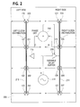
- FIG. 2 illustrates an example disadvantageous two clock distribution spine arrangement in an integrated circuit die.
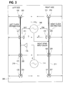
- FIG. 3 illustrates an example of a two clock distribution spine arrangement in an integrated circuit die in accordance with an example embodiment of the present invention.
- clock distribution network skew is determined by two main factors, namely, clock line delay and clock driver delay variations over the die due to process variations.
- the clock signal distribution in a large integrated circuit die requires long clock lines that becomes the major contributor to the clock signal skew.
- One technique used to decrease the clock network distribution skew is to split the clock network into two networks. Each network distributes the clock signal to one-half of the die so that the clock line lengths are shortened, thereby reducing the clock skew.
- the delay from the common input from the clock signal generator to each network output varies due to die process variations within the integrated circuit die, these variations affecting the delay of the various clock buffer amplifiers. Accordingly, the clock signal on one of the two networks is skewed with respect to the clock signal on the other of the two networks unless a phase de-skewing mechanism is added to match the two network delays.
- FIG. 2 illustrates an example of a disadvantageous two clock distribution spine arrangement in an integrated circuit die.
- Buffer amplifiers 120 , 121 , 122 , 123 , 220 , 221 , 222 , and 223 receive and distribute the clock signal from the left clock distribution spine 210 to various points on the left side of the die.
- buffer amplifiers 124 , 125 , 126 , 127 , 224 , 225 , 226 , and 227 receive and distribute the clock signal from the right clock distribution spine 211 to various points on the right side of the die.
- the clock signal generated by the clock signal generator 114 is fed to the left clock distribution spine 210 by the buffer amplifier 115 and is fed to the right clock distribution spine 211 by the variable delay buffer amplifier 230 which will be discussed below.
- a phase detector 240 is disposed within the die to detect the phase difference between the clock signal at point C and the clock signal at point B.
- the output of the phase detector is fed to the variable delay buffer 230 .
- the variable delay buffer 230 is a passive phase de-skew device which is programmed by the phase detector 240 during reset of the integrated circuit and the amount of delay added by the variable delay buffer 230 is unchanged during operation of the integrated circuit until another reset occurs.
- a disadvantage of the arrangement of FIG. 2 is that there is no correction for any phase variations between the left clock distribution spine 210 and the right clock distribution spine 211 due to voltage or temperature variations that occur after the delay in the variable delay buffer 230 has been set.
- FIG. 3 illustrates an example of a two clock distribution spine arrangement in an integrated circuit die in accordance with an example embodiment of the present invention.
- the arrangement differs from FIG. 2 in that the phase detector 240 and variable delay buffer 230 of FIG. 2 have been replaced by a 1:1 PLL (Phase Locked Loop) 340 disposed within the integrated circuit die 300 .
- the PLL 340 which has a wide bandwidth, is used to de-skew the phase of the two distribution spines.
- a REF (Reference) input of the PLL 340 is connected directly to the left clock distribution spine 210 while the FBK (Feedback) input of the PLL 340 is connected to the right clock distribution spine 211 .
- the output of the PLL 340 becomes the right spine input clock.
- the PLL 340 operates to minimize the skew between its reference signal phase input and its feedback signal phase input so that the clock signals on the two clock distribution spines are de-skewed.
- the PLL 340 is continuously active so that the phase de-skew operation continues all the time, thereby allowing the PLL 340 to track reference clock phase variations due to voltage and temperature variations over time.
- the PLL 340 acts as a filter by reducing Vcc noise frequencies inside the PLL bandwidth.
- the output of the PLL 340 is less sensitive to Vcc noise as compared to the phase detector 240 due to the low coupling of the PLL 340 to Vcc.
- FIG. 3 illustrates a two clock distribution spine arrangement
- the present invention is not limited to two clock distribution spines but rather can be applied to any number of clock distribution spines by merely providing a PLL for each clock distribution spine other than the one spine that is used as the reference for each PLL.
Abstract
Description
Claims (25)
Priority Applications (1)
| Application Number | Priority Date | Filing Date | Title |
|---|---|---|---|
| US09/819,716 US6630855B2 (en) | 2001-03-29 | 2001-03-29 | Clock distribution phase alignment technique |
Applications Claiming Priority (1)
| Application Number | Priority Date | Filing Date | Title |
|---|---|---|---|
| US09/819,716 US6630855B2 (en) | 2001-03-29 | 2001-03-29 | Clock distribution phase alignment technique |
Publications (2)
| Publication Number | Publication Date |
|---|---|
| US20020140487A1 US20020140487A1 (en) | 2002-10-03 |
| US6630855B2 true US6630855B2 (en) | 2003-10-07 |
Family
ID=25228852
Family Applications (1)
| Application Number | Title | Priority Date | Filing Date |
|---|---|---|---|
| US09/819,716 Expired - Fee Related US6630855B2 (en) | 2001-03-29 | 2001-03-29 | Clock distribution phase alignment technique |
Country Status (1)
| Country | Link |
|---|---|
| US (1) | US6630855B2 (en) |
Cited By (14)
| Publication number | Priority date | Publication date | Assignee | Title |
|---|---|---|---|---|
| US20050030071A1 (en) * | 2003-08-04 | 2005-02-10 | Rambus Inc. | Phase synchronization for wide area integrated circuits |
| US20050207553A1 (en) * | 2004-03-18 | 2005-09-22 | Alcatel | Service provisioning system |
| US20050258881A1 (en) * | 2004-05-19 | 2005-11-24 | Lsi Logic Corporation | Chip level clock tree deskew circuit |
| US20070120588A1 (en) * | 2005-11-30 | 2007-05-31 | Lim Chee H | Low-jitter clock distribution |
| US20090015311A1 (en) * | 2007-07-11 | 2009-01-15 | United Memories, Inc. | Low skew clock distribution tree |
| US7605668B2 (en) | 2006-12-12 | 2009-10-20 | Intel Corporation | Delay stage with controllably variable capacitive load |
| US7765425B1 (en) * | 2006-03-21 | 2010-07-27 | GlobalFoundries, Inc. | Incrementally adjustable skew and duty cycle correction for clock signals within a clock distribution network |
| US7770049B1 (en) * | 2006-03-21 | 2010-08-03 | Advanced Micro Devices, Inc. | Controller for clock skew determination and reduction based on a lead count over multiple clock cycles |
| US8205182B1 (en) | 2007-08-22 | 2012-06-19 | Cadence Design Systems, Inc. | Automatic synthesis of clock distribution networks |
| US8817936B2 (en) | 2012-05-23 | 2014-08-26 | The Boeing Company | Multiple synchronous IQ demodulators |
| US20140289550A1 (en) * | 2013-03-25 | 2014-09-25 | Lsi Corporation | Integrated Clock Architecture for Improved Testing |
| US8937491B2 (en) * | 2012-11-15 | 2015-01-20 | Xilinx, Inc. | Clock network architecture |
| US20150338877A1 (en) * | 2014-05-22 | 2015-11-26 | Global Unichip Corporation | Integrated circuit |
| US10218360B2 (en) * | 2016-08-02 | 2019-02-26 | Altera Corporation | Dynamic clock-data phase alignment in a source synchronous interface circuit |
Families Citing this family (5)
| Publication number | Priority date | Publication date | Assignee | Title |
|---|---|---|---|---|
| JP2007336003A (en) * | 2006-06-12 | 2007-12-27 | Nec Electronics Corp | Clock distribution circuit, forming method thereof, semiconductor integrated circuit, and program thereof |
| US7719316B2 (en) * | 2006-12-01 | 2010-05-18 | The Regents Of The University Of Michigan | Clock distribution network architecture for resonant-clocked systems |
| US7973565B2 (en) * | 2007-05-23 | 2011-07-05 | Cyclos Semiconductor, Inc. | Resonant clock and interconnect architecture for digital devices with multiple clock networks |
| JP2010073761A (en) * | 2008-09-17 | 2010-04-02 | Fujitsu Ltd | Semiconductor device, and method of controlling the same |
| US8358163B2 (en) * | 2009-10-12 | 2013-01-22 | Cyclos Semiconductor, Inc. | Resonant clock distribution network architecture for tracking parameter variations in conventional clock distribution networks |
Citations (5)
| Publication number | Priority date | Publication date | Assignee | Title |
|---|---|---|---|---|
| US5420544A (en) * | 1992-12-28 | 1995-05-30 | Mitsubishi Denki Kabushiki Kaisha | Semiconductor integrated circuit, method of designing the same and method of manufacturing the same |
| US5465347A (en) * | 1990-09-05 | 1995-11-07 | International Business Machines Corporation | System for reducing phase difference between clock signals of integrated circuit chips by comparing clock signal from one chip to clock signal from another chip |
| US5880612A (en) * | 1996-10-17 | 1999-03-09 | Samsung Electronics Co., Ltd. | Signal de-skewing using programmable dual delay-locked loop |
| US5949262A (en) | 1998-01-07 | 1999-09-07 | International Business Machines Corporation | Method and apparatus for coupled phase locked loops |
| US6075832A (en) * | 1997-10-07 | 2000-06-13 | Intel Corporation | Method and apparatus for deskewing clock signals |
-
2001
- 2001-03-29 US US09/819,716 patent/US6630855B2/en not_active Expired - Fee Related
Patent Citations (5)
| Publication number | Priority date | Publication date | Assignee | Title |
|---|---|---|---|---|
| US5465347A (en) * | 1990-09-05 | 1995-11-07 | International Business Machines Corporation | System for reducing phase difference between clock signals of integrated circuit chips by comparing clock signal from one chip to clock signal from another chip |
| US5420544A (en) * | 1992-12-28 | 1995-05-30 | Mitsubishi Denki Kabushiki Kaisha | Semiconductor integrated circuit, method of designing the same and method of manufacturing the same |
| US5880612A (en) * | 1996-10-17 | 1999-03-09 | Samsung Electronics Co., Ltd. | Signal de-skewing using programmable dual delay-locked loop |
| US6075832A (en) * | 1997-10-07 | 2000-06-13 | Intel Corporation | Method and apparatus for deskewing clock signals |
| US5949262A (en) | 1998-01-07 | 1999-09-07 | International Business Machines Corporation | Method and apparatus for coupled phase locked loops |
Cited By (25)
| Publication number | Priority date | Publication date | Assignee | Title |
|---|---|---|---|---|
| US20050030071A1 (en) * | 2003-08-04 | 2005-02-10 | Rambus Inc. | Phase synchronization for wide area integrated circuits |
| US6861884B1 (en) * | 2003-08-04 | 2005-03-01 | Rambus Inc. | Phase synchronization for wide area integrated circuits |
| US20050046454A1 (en) * | 2003-08-04 | 2005-03-03 | Nguyen Huy M. | Phase synchronization for wide area integrated circuits |
| US7161400B2 (en) | 2003-08-04 | 2007-01-09 | Rambus Inc. | Phase synchronization for wide area integrated circuits |
| US20070124636A1 (en) * | 2003-08-04 | 2007-05-31 | Rambus Inc. | Phase synchronization for wide area integrated circuits |
| US7932755B2 (en) | 2003-08-04 | 2011-04-26 | Rambus Inc. | Phase synchronization for wide area integrated circuits |
| US20050207553A1 (en) * | 2004-03-18 | 2005-09-22 | Alcatel | Service provisioning system |
| US20050258881A1 (en) * | 2004-05-19 | 2005-11-24 | Lsi Logic Corporation | Chip level clock tree deskew circuit |
| US7023252B2 (en) * | 2004-05-19 | 2006-04-04 | Lsi Logic Corporation | Chip level clock tree deskew circuit |
| US20070120588A1 (en) * | 2005-11-30 | 2007-05-31 | Lim Chee H | Low-jitter clock distribution |
| US7765425B1 (en) * | 2006-03-21 | 2010-07-27 | GlobalFoundries, Inc. | Incrementally adjustable skew and duty cycle correction for clock signals within a clock distribution network |
| US7770049B1 (en) * | 2006-03-21 | 2010-08-03 | Advanced Micro Devices, Inc. | Controller for clock skew determination and reduction based on a lead count over multiple clock cycles |
| US7605668B2 (en) | 2006-12-12 | 2009-10-20 | Intel Corporation | Delay stage with controllably variable capacitive load |
| US7586355B2 (en) * | 2007-07-11 | 2009-09-08 | United Memories, Inc. | Low skew clock distribution tree |
| US20090015311A1 (en) * | 2007-07-11 | 2009-01-15 | United Memories, Inc. | Low skew clock distribution tree |
| US8205182B1 (en) | 2007-08-22 | 2012-06-19 | Cadence Design Systems, Inc. | Automatic synthesis of clock distribution networks |
| US8817936B2 (en) | 2012-05-23 | 2014-08-26 | The Boeing Company | Multiple synchronous IQ demodulators |
| US8937491B2 (en) * | 2012-11-15 | 2015-01-20 | Xilinx, Inc. | Clock network architecture |
| US20140289550A1 (en) * | 2013-03-25 | 2014-09-25 | Lsi Corporation | Integrated Clock Architecture for Improved Testing |
| US9251916B2 (en) * | 2013-03-25 | 2016-02-02 | Avago Technologies General Ip (Singapore) Pte. Ltd. | Integrated clock architecture for improved testing |
| US20150338877A1 (en) * | 2014-05-22 | 2015-11-26 | Global Unichip Corporation | Integrated circuit |
| US9513659B2 (en) * | 2014-05-22 | 2016-12-06 | Global Unichip Corporation | Integrated circuit |
| US10218360B2 (en) * | 2016-08-02 | 2019-02-26 | Altera Corporation | Dynamic clock-data phase alignment in a source synchronous interface circuit |
| US20190149154A1 (en) * | 2016-08-02 | 2019-05-16 | Altera Corporation | Dynamic clock-data phase alignment in a source synchronous interface circuit |
| US10439615B2 (en) * | 2016-08-02 | 2019-10-08 | Altera Corporation | Dynamic clock-data phase alignment in a source synchronous interface circuit |
Also Published As
| Publication number | Publication date |
|---|---|
| US20020140487A1 (en) | 2002-10-03 |
Similar Documents
| Publication | Publication Date | Title |
|---|---|---|
| US6630855B2 (en) | Clock distribution phase alignment technique | |
| US6894933B2 (en) | Buffer amplifier architecture for semiconductor memory circuits | |
| JP2636677B2 (en) | Semiconductor integrated circuit | |
| US6469555B1 (en) | Apparatus and method for generating multiple clock signals from a single loop circuit | |
| US6496445B2 (en) | Semiconductor memory device having altered clock frequency for address and/or command signals, and memory module and system having the same | |
| US8446196B2 (en) | Input interface circuit | |
| US7721137B2 (en) | Bus receiver and method of deskewing bus signals | |
| US20080285375A1 (en) | Semiconductor device, module including the semiconductor device, and system including the module | |
| US6832325B2 (en) | Device on a source synchronous bus sending data in quadrature phase relationship and receiving data in phase with the bus clock signal | |
| US6346830B1 (en) | Data input/output circuit and interface system using the same | |
| KR100705502B1 (en) | Clock generating apparatus and clock receiving apparatus for eliminating the difference of generated clocks | |
| US8134391B2 (en) | Semiconductor devices with signal synchronization circuits | |
| US20040101079A1 (en) | Delay-lock-loop with improved accuracy and range | |
| US8001507B2 (en) | Electric circuit and method for adjusting wirelength of clock signal in electric circuit | |
| US6535038B2 (en) | Reduced jitter clock generator circuit and method for applying properly phased clock signals to clocked devices | |
| US6242955B1 (en) | Delay lock loop circuit, system and method for synchronizing a reference signal with an output signal | |
| US6157238A (en) | Clock system of a semiconductor memory device employing a frequency amplifier | |
| US6810486B2 (en) | Method and apparatus for de-skewing a clock using a first and second phase locked loop and a clock tree | |
| US6255883B1 (en) | System and method for balancing clock distribution between two devices | |
| JP2927273B2 (en) | Clock skew correction circuit | |
| US6744293B1 (en) | Global clock tree de-skew | |
| US6356100B1 (en) | Ground bounce reduction technique using phased outputs and package de-skewing for synchronous buses | |
| KR100242591B1 (en) | Apparatus having skew compensation circuit and control method thereof | |
| US6414539B1 (en) | AC timings at the input buffer of source synchronous and common clock designs by making the supply for differential amplifier track the reference voltage | |
| JPH11225172A (en) | Circuit and method for correcting pulse width |
Legal Events
| Date | Code | Title | Description |
|---|---|---|---|
| AS | Assignment |
Owner name: INTEL CORP., CALIFORNIA Free format text: ASSIGNMENT OF ASSIGNORS INTEREST;ASSIGNORS:FAYNEH, EYAL;KNOL, ERNEST;REEL/FRAME:011957/0550 Effective date: 20010610 |
|
| CC | Certificate of correction | ||
| FEPP | Fee payment procedure |
Free format text: PAYOR NUMBER ASSIGNED (ORIGINAL EVENT CODE: ASPN); ENTITY STATUS OF PATENT OWNER: LARGE ENTITY |
|
| FPAY | Fee payment |
Year of fee payment: 4 |
|
| FPAY | Fee payment |
Year of fee payment: 8 |
|
| SULP | Surcharge for late payment |
Year of fee payment: 7 |
|
| REMI | Maintenance fee reminder mailed | ||
| LAPS | Lapse for failure to pay maintenance fees | ||
| STCH | Information on status: patent discontinuation |
Free format text: PATENT EXPIRED DUE TO NONPAYMENT OF MAINTENANCE FEES UNDER 37 CFR 1.362 |
|
| FP | Lapsed due to failure to pay maintenance fee |
Effective date: 20151007 |