US6707328B2 - Semiconductor integrated circuit related to a circuit operating on the basis of a clock signal - Google Patents
Semiconductor integrated circuit related to a circuit operating on the basis of a clock signal Download PDFInfo
- Publication number
- US6707328B2 US6707328B2 US09/745,990 US74599000A US6707328B2 US 6707328 B2 US6707328 B2 US 6707328B2 US 74599000 A US74599000 A US 74599000A US 6707328 B2 US6707328 B2 US 6707328B2
- Authority
- US
- United States
- Prior art keywords
- power supply
- potential side
- circuit
- supply wire
- semiconductor substrate
- Prior art date
- Legal status (The legal status is an assumption and is not a legal conclusion. Google has not performed a legal analysis and makes no representation as to the accuracy of the status listed.)
- Expired - Lifetime
Links
Images


Classifications
-
- H—ELECTRICITY
- H03—ELECTRONIC CIRCUITRY
- H03K—PULSE TECHNIQUE
- H03K3/00—Circuits for generating electric pulses; Monostable, bistable or multistable circuits
- H03K3/01—Details
- H03K3/013—Modifications of generator to prevent operation by noise or interference
-
- H—ELECTRICITY
- H01—ELECTRIC ELEMENTS
- H01L—SEMICONDUCTOR DEVICES NOT COVERED BY CLASS H10
- H01L27/00—Devices consisting of a plurality of semiconductor or other solid-state components formed in or on a common substrate
- H01L27/02—Devices consisting of a plurality of semiconductor or other solid-state components formed in or on a common substrate including semiconductor components specially adapted for rectifying, oscillating, amplifying or switching and having at least one potential-jump barrier or surface barrier; including integrated passive circuit elements with at least one potential-jump barrier or surface barrier
- H01L27/0203—Particular design considerations for integrated circuits
- H01L27/0207—Geometrical layout of the components, e.g. computer aided design; custom LSI, semi-custom LSI, standard cell technique
-
- H—ELECTRICITY
- H01—ELECTRIC ELEMENTS
- H01L—SEMICONDUCTOR DEVICES NOT COVERED BY CLASS H10
- H01L27/00—Devices consisting of a plurality of semiconductor or other solid-state components formed in or on a common substrate
- H01L27/02—Devices consisting of a plurality of semiconductor or other solid-state components formed in or on a common substrate including semiconductor components specially adapted for rectifying, oscillating, amplifying or switching and having at least one potential-jump barrier or surface barrier; including integrated passive circuit elements with at least one potential-jump barrier or surface barrier
- H01L27/04—Devices consisting of a plurality of semiconductor or other solid-state components formed in or on a common substrate including semiconductor components specially adapted for rectifying, oscillating, amplifying or switching and having at least one potential-jump barrier or surface barrier; including integrated passive circuit elements with at least one potential-jump barrier or surface barrier the substrate being a semiconductor body
- H01L27/10—Devices consisting of a plurality of semiconductor or other solid-state components formed in or on a common substrate including semiconductor components specially adapted for rectifying, oscillating, amplifying or switching and having at least one potential-jump barrier or surface barrier; including integrated passive circuit elements with at least one potential-jump barrier or surface barrier the substrate being a semiconductor body including a plurality of individual components in a repetitive configuration
- H01L27/118—Masterslice integrated circuits
- H01L27/11803—Masterslice integrated circuits using field effect technology
- H01L27/11807—CMOS gate arrays
-
- H—ELECTRICITY
- H03—ELECTRONIC CIRCUITRY
- H03K—PULSE TECHNIQUE
- H03K19/00—Logic circuits, i.e. having at least two inputs acting on one output; Inverting circuits
- H03K19/003—Modifications for increasing the reliability for protection
- H03K19/00346—Modifications for eliminating interference or parasitic voltages or currents
- H03K19/00361—Modifications for eliminating interference or parasitic voltages or currents in field effect transistor circuits
-
- H—ELECTRICITY
- H03—ELECTRONIC CIRCUITRY
- H03K—PULSE TECHNIQUE
- H03K3/00—Circuits for generating electric pulses; Monostable, bistable or multistable circuits
- H03K3/02—Generators characterised by the type of circuit or by the means used for producing pulses
- H03K3/027—Generators characterised by the type of circuit or by the means used for producing pulses by the use of logic circuits, with internal or external positive feedback
- H03K3/037—Bistable circuits
- H03K3/0372—Bistable circuits of the master-slave type
Definitions
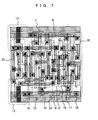
- the semiconductor integrated circuit 1 is provided therein with a plurality of logic circuits 6 synchronously designed to operate in synchronization with the clock signal CK, a first power supply wire 7 for supplying the power supply voltage VDD from the first input terminal 2 to a clock signal inversion circuit, described later, of each logic circuit 6 , a second power supply wire 8 for supplying the power supply voltage VDD from the second input terminal 3 to each logic circuit 6 , a third power supply wire 9 for supplying the power supply voltage VSS from the third input terminal 4 to each logic circuit 6 and a clock input wire 10 for inputting the clock signal CK from the clock input terminal 5 in each logic circuit 6 .
- the semiconductor integrated circuit 1 has a multilayer structure.
- the third device region 34 is provided with a third P-type transistor group 45 and a third N-type transistor group 46 .
Abstract
Description
Claims (14)
Priority Applications (1)
| Application Number | Priority Date | Filing Date | Title |
|---|---|---|---|
| US10/760,475 US7081778B2 (en) | 1999-12-28 | 2004-01-21 | Semiconductor integrated circuit related to a circuit operating on the basis of a clock signal |
Applications Claiming Priority (2)
| Application Number | Priority Date | Filing Date | Title |
|---|---|---|---|
| JP37278199A JP2001189423A (en) | 1999-12-28 | 1999-12-28 | Semiconductor interpreted circuit |
| JP11-372781 | 1999-12-28 |
Related Child Applications (1)
| Application Number | Title | Priority Date | Filing Date |
|---|---|---|---|
| US10/760,475 Continuation US7081778B2 (en) | 1999-12-28 | 2004-01-21 | Semiconductor integrated circuit related to a circuit operating on the basis of a clock signal |
Publications (2)
| Publication Number | Publication Date |
|---|---|
| US20010005153A1 US20010005153A1 (en) | 2001-06-28 |
| US6707328B2 true US6707328B2 (en) | 2004-03-16 |
Family
ID=18501040
Family Applications (2)
| Application Number | Title | Priority Date | Filing Date |
|---|---|---|---|
| US09/745,990 Expired - Lifetime US6707328B2 (en) | 1999-12-28 | 2000-12-26 | Semiconductor integrated circuit related to a circuit operating on the basis of a clock signal |
| US10/760,475 Expired - Lifetime US7081778B2 (en) | 1999-12-28 | 2004-01-21 | Semiconductor integrated circuit related to a circuit operating on the basis of a clock signal |
Family Applications After (1)
| Application Number | Title | Priority Date | Filing Date |
|---|---|---|---|
| US10/760,475 Expired - Lifetime US7081778B2 (en) | 1999-12-28 | 2004-01-21 | Semiconductor integrated circuit related to a circuit operating on the basis of a clock signal |
Country Status (2)
| Country | Link |
|---|---|
| US (2) | US6707328B2 (en) |
| JP (1) | JP2001189423A (en) |
Cited By (2)
| Publication number | Priority date | Publication date | Assignee | Title |
|---|---|---|---|---|
| US7081778B2 (en) * | 1999-12-28 | 2006-07-25 | Sanyo Electric Co., Ltd. | Semiconductor integrated circuit related to a circuit operating on the basis of a clock signal |
| US20060176099A1 (en) * | 2005-02-07 | 2006-08-10 | Fujitsu Limited | Semiconductor integrated circuit and method of controlling the semiconductor integrated circuit |
Families Citing this family (16)
| Publication number | Priority date | Publication date | Assignee | Title |
|---|---|---|---|---|
| US8095903B2 (en) * | 2004-06-01 | 2012-01-10 | Pulsic Limited | Automatically routing nets with variable spacing |
| TWI344625B (en) | 2005-03-08 | 2011-07-01 | Epson Imaging Devices Corp | Driving circuit of display device, driving circuit of electro-optical device, and electronic apparatus |
| TWI337006B (en) * | 2007-04-14 | 2011-02-01 | Raydium Semiconductor Corp | Flip-flop and shift register |
| JP5773379B2 (en) * | 2009-03-19 | 2015-09-02 | ソニー株式会社 | SEMICONDUCTOR DEVICE, ITS MANUFACTURING METHOD, AND ELECTRONIC DEVICE |
| JP5985136B2 (en) * | 2009-03-19 | 2016-09-06 | ソニー株式会社 | SEMICONDUCTOR DEVICE, ITS MANUFACTURING METHOD, AND ELECTRONIC DEVICE |
| CN102361440B (en) * | 2011-10-21 | 2013-03-27 | 中国人民解放军国防科学技术大学 | Single-event-upset resistant scan structure D trigger capable of being reset synchronously |
| CN102394598B (en) * | 2011-10-21 | 2013-12-11 | 中国人民解放军国防科学技术大学 | Single event upset resistant synchronously resettable D flip-flop |
| CN102394601B (en) * | 2011-10-21 | 2013-12-11 | 中国人民解放军国防科学技术大学 | D trigger provided with scanning structure and resisting single event upset |
| CN102394596B (en) * | 2011-10-21 | 2013-12-11 | 中国人民解放军国防科学技术大学 | Signal event upset resistance D trigger capable of being set |
| CN102394600B (en) * | 2011-10-21 | 2013-12-11 | 中国人民解放军国防科学技术大学 | Signal particle upset resistance D trigger capable of being set and reset |
| CN102394599B (en) * | 2011-10-21 | 2013-12-11 | 中国人民解放军国防科学技术大学 | Single event upset resistant settable and resettable scan structure D flip-flop |
| CN102394595B (en) * | 2011-10-21 | 2013-12-11 | 中国人民解放军国防科学技术大学 | Settable and resettable D trigger resisting single event upset |
| CN102394597B (en) * | 2011-10-21 | 2013-12-11 | 中国人民解放军国防科学技术大学 | D trigger resisting single event upset |
| CN102394602B (en) * | 2011-10-21 | 2013-12-11 | 中国人民解放军国防科学技术大学 | Single event upset-resisting scanning structure D trigger capable of setting and resetting |
| CN105468798B (en) * | 2014-09-02 | 2019-06-21 | 复旦大学 | A kind of anti-radiation placement-and-routing's method of integrated circuit |
| CN112115670A (en) * | 2020-08-31 | 2020-12-22 | 深圳天狼芯半导体有限公司 | Power network layout method and device of chip |
Citations (13)
| Publication number | Priority date | Publication date | Assignee | Title |
|---|---|---|---|---|
| JPS612342A (en) | 1984-06-15 | 1986-01-08 | Hitachi Ltd | Semiconductor integrated circuit device |
| US4988893A (en) * | 1986-12-30 | 1991-01-29 | International Business Machines Corporation | Latch cell family in CMOS technology gate array |
| JPH0393237A (en) | 1989-09-06 | 1991-04-18 | Sony Corp | Ccd device |
| US5289518A (en) * | 1991-07-25 | 1994-02-22 | Sharp Kabushiki Kaisha | Low power shift register circuit |
| US5296757A (en) * | 1992-01-09 | 1994-03-22 | Kabushiki Kaisha Toshiba | Low-noise output driver having separate supply lines and sequenced operation for transient and steady-state portions |
| JPH06310656A (en) | 1993-04-27 | 1994-11-04 | Hitachi Ltd | Semiconductor integrated circuit |
| US5382846A (en) * | 1991-12-13 | 1995-01-17 | Kabushiki Kaisha Toshiba | Level shifting circuit for suppressing output amplitude |
| JPH08125025A (en) | 1994-10-28 | 1996-05-17 | Matsushita Electric Ind Co Ltd | Microcomputer core and its layout method |
| US5576643A (en) * | 1994-12-09 | 1996-11-19 | Fujitsu Limited | Data transfer circuit device |
| US5923187A (en) * | 1996-01-18 | 1999-07-13 | U.S. Philips Corporation | Multidirectional data transmission device |
| JPH11204649A (en) | 1998-01-13 | 1999-07-30 | Toshiba Corp | Semiconductor integrated circuit |
| US5990706A (en) * | 1996-03-29 | 1999-11-23 | Kabushiki Kaisha Toshiba | Logic circuit and method of designing the same |
| US6380764B1 (en) * | 1997-12-26 | 2002-04-30 | Hitachi, Ltd. | Semiconductor integrated circuit device, recording medium stored with cell library, and method for designing semiconductor integrated circuit |
Family Cites Families (2)
| Publication number | Priority date | Publication date | Assignee | Title |
|---|---|---|---|---|
| JPH03932A (en) | 1989-02-10 | 1991-01-07 | Toshiba Corp | Control process of turbo machine and controller thereof |
| JP2001189423A (en) * | 1999-12-28 | 2001-07-10 | Sanyo Electric Co Ltd | Semiconductor interpreted circuit |
-
1999
- 1999-12-28 JP JP37278199A patent/JP2001189423A/en active Pending
-
2000
- 2000-12-26 US US09/745,990 patent/US6707328B2/en not_active Expired - Lifetime
-
2004
- 2004-01-21 US US10/760,475 patent/US7081778B2/en not_active Expired - Lifetime
Patent Citations (14)
| Publication number | Priority date | Publication date | Assignee | Title |
|---|---|---|---|---|
| JPS612342A (en) | 1984-06-15 | 1986-01-08 | Hitachi Ltd | Semiconductor integrated circuit device |
| US4988893A (en) * | 1986-12-30 | 1991-01-29 | International Business Machines Corporation | Latch cell family in CMOS technology gate array |
| JPH0393237A (en) | 1989-09-06 | 1991-04-18 | Sony Corp | Ccd device |
| US5124796A (en) | 1989-09-06 | 1992-06-23 | Sony Corporation | Charge coupled device having a circuit for handling a fundamental clock signal |
| US5289518A (en) * | 1991-07-25 | 1994-02-22 | Sharp Kabushiki Kaisha | Low power shift register circuit |
| US5382846A (en) * | 1991-12-13 | 1995-01-17 | Kabushiki Kaisha Toshiba | Level shifting circuit for suppressing output amplitude |
| US5296757A (en) * | 1992-01-09 | 1994-03-22 | Kabushiki Kaisha Toshiba | Low-noise output driver having separate supply lines and sequenced operation for transient and steady-state portions |
| JPH06310656A (en) | 1993-04-27 | 1994-11-04 | Hitachi Ltd | Semiconductor integrated circuit |
| JPH08125025A (en) | 1994-10-28 | 1996-05-17 | Matsushita Electric Ind Co Ltd | Microcomputer core and its layout method |
| US5576643A (en) * | 1994-12-09 | 1996-11-19 | Fujitsu Limited | Data transfer circuit device |
| US5923187A (en) * | 1996-01-18 | 1999-07-13 | U.S. Philips Corporation | Multidirectional data transmission device |
| US5990706A (en) * | 1996-03-29 | 1999-11-23 | Kabushiki Kaisha Toshiba | Logic circuit and method of designing the same |
| US6380764B1 (en) * | 1997-12-26 | 2002-04-30 | Hitachi, Ltd. | Semiconductor integrated circuit device, recording medium stored with cell library, and method for designing semiconductor integrated circuit |
| JPH11204649A (en) | 1998-01-13 | 1999-07-30 | Toshiba Corp | Semiconductor integrated circuit |
Non-Patent Citations (2)
| Title |
|---|
| Japanese Notification of Reason(s) for Refusal (Oct. 29, 2002) w/translation. |
| Notification of Reasons for Refusal dated Aug 19, 2003 from the Japanese Patent Office for Japanese Laid Open Patent Application No. 11-372781 and translation. |
Cited By (2)
| Publication number | Priority date | Publication date | Assignee | Title |
|---|---|---|---|---|
| US7081778B2 (en) * | 1999-12-28 | 2006-07-25 | Sanyo Electric Co., Ltd. | Semiconductor integrated circuit related to a circuit operating on the basis of a clock signal |
| US20060176099A1 (en) * | 2005-02-07 | 2006-08-10 | Fujitsu Limited | Semiconductor integrated circuit and method of controlling the semiconductor integrated circuit |
Also Published As
| Publication number | Publication date |
|---|---|
| US7081778B2 (en) | 2006-07-25 |
| JP2001189423A (en) | 2001-07-10 |
| US20010005153A1 (en) | 2001-06-28 |
| US20040150442A1 (en) | 2004-08-05 |
Similar Documents
| Publication | Publication Date | Title |
|---|---|---|
| US6707328B2 (en) | Semiconductor integrated circuit related to a circuit operating on the basis of a clock signal | |
| JP4036688B2 (en) | Standard cell library for automatic placement and routing and semiconductor integrated device | |
| US6765245B2 (en) | Gate array core cell for VLSI ASIC devices | |
| US7538368B2 (en) | Standard cell, standard cell library, and semiconductor integrated circuit with suppressed variation in characteristics | |
| EP0093003B1 (en) | Gate array large scale integrated circuit devices | |
| JPH03165061A (en) | Semiconductor integrated circuit device | |
| JPH0434309B2 (en) | ||
| JPH0480538B2 (en) | ||
| JP3115787B2 (en) | Polycell integrated circuit | |
| JP4743469B2 (en) | Semiconductor integrated circuit device and clock distribution method | |
| JP3644138B2 (en) | Semiconductor integrated circuit and placement and routing method thereof | |
| JP2003060060A (en) | Semiconductor integrated circuit device | |
| JP3651944B2 (en) | CMOS cell | |
| JPH0831581B2 (en) | Semiconductor device | |
| US6720214B2 (en) | Method for manufacturing semiconductor integrated circuit | |
| JP4081047B2 (en) | Wired trimmed programmable logic array | |
| JPH0316790B2 (en) | ||
| US7185307B2 (en) | Method of fabricating and integrated circuit through utilizing metal layers to program randomly positioned basic units | |
| JP2671883B2 (en) | Semiconductor integrated circuit device | |
| JPH073863B2 (en) | Semiconductor integrated circuit | |
| JPS5972742A (en) | Master method of master slice lsi | |
| JPS61190958A (en) | Semiconductor integrated circuit | |
| JPH0834427B2 (en) | Logic circuit | |
| KR920005798B1 (en) | Borderless master slice semiconductor device | |
| JPS63232352A (en) | Master slice type semiconductor integrated circuit |
Legal Events
| Date | Code | Title | Description |
|---|---|---|---|
| AS | Assignment |
Owner name: SANYO ELECTRIC CO., LTD., JAPAN Free format text: ASSIGNMENT OF ASSIGNORS INTEREST;ASSIGNORS:UEDA, YOSHITAKA;OGURA, ISAO;REEL/FRAME:011394/0520 Effective date: 20001219 |
|
| AS | Assignment |
Owner name: SANYO ELECTRIC CO., LTD., JAPAN Free format text: RE-RECORD TO CORRECT THE ASSIGNEE'S ADDRESS, PREVIOUSLY RECORDED ON REEL 011394 FRAME 0520, ASSIGNOR CONFIRMS THE ASSIGNMENT OF THE ENTIRE INTEREST.;ASSIGNORS:UEDA, YOSHITAKA;OGURA, ISAO;REEL/FRAME:011779/0102 Effective date: 20001219 |
|
| FEPP | Fee payment procedure |
Free format text: PAYER NUMBER DE-ASSIGNED (ORIGINAL EVENT CODE: RMPN); ENTITY STATUS OF PATENT OWNER: LARGE ENTITY Free format text: PAYOR NUMBER ASSIGNED (ORIGINAL EVENT CODE: ASPN); ENTITY STATUS OF PATENT OWNER: LARGE ENTITY |
|
| STCF | Information on status: patent grant |
Free format text: PATENTED CASE |
|
| FPAY | Fee payment |
Year of fee payment: 4 |
|
| FEPP | Fee payment procedure |
Free format text: PAYOR NUMBER ASSIGNED (ORIGINAL EVENT CODE: ASPN); ENTITY STATUS OF PATENT OWNER: LARGE ENTITY |
|
| AS | Assignment |
Owner name: SEMICONDUCTOR COMPONENTS INDUSTRIES, LLC, ARIZONA Free format text: ASSIGNMENT OF ASSIGNORS INTEREST;ASSIGNOR:SANYO ELECTRIC CO., LTD.;REEL/FRAME:026594/0385 Effective date: 20110101 |
|
| FPAY | Fee payment |
Year of fee payment: 8 |
|
| AS | Assignment |
Owner name: SEMICONDUCTOR COMPONENTS INDUSTRIES, LLC, ARIZONA Free format text: CORRECTIVE ASSIGNMENT TO CORRECT THE INCORRECT #12/577882 PREVIOUSLY RECORDED ON REEL 026594 FRAME 0385. ASSIGNOR(S) HEREBY CONFIRMS THE ASSIGNMENT;ASSIGNOR:SANYO ELECTRIC CO., LTD;REEL/FRAME:032836/0342 Effective date: 20110101 |
|
| FPAY | Fee payment |
Year of fee payment: 12 |
|
| AS | Assignment |
Owner name: DEUTSCHE BANK AG NEW YORK BRANCH, NEW YORK Free format text: SECURITY INTEREST;ASSIGNOR:SEMICONDUCTOR COMPONENTS INDUSTRIES, LLC;REEL/FRAME:038620/0087 Effective date: 20160415 |
|
| AS | Assignment |
Owner name: DEUTSCHE BANK AG NEW YORK BRANCH, AS COLLATERAL AG Free format text: CORRECTIVE ASSIGNMENT TO CORRECT THE INCORRECT PATENT NUMBER 5859768 AND TO RECITE COLLATERAL AGENT ROLE OF RECEIVING PARTY IN THE SECURITY INTEREST PREVIOUSLY RECORDED ON REEL 038620 FRAME 0087. ASSIGNOR(S) HEREBY CONFIRMS THE SECURITY INTEREST;ASSIGNOR:SEMICONDUCTOR COMPONENTS INDUSTRIES, LLC;REEL/FRAME:039853/0001 Effective date: 20160415 Owner name: DEUTSCHE BANK AG NEW YORK BRANCH, AS COLLATERAL AGENT, NEW YORK Free format text: CORRECTIVE ASSIGNMENT TO CORRECT THE INCORRECT PATENT NUMBER 5859768 AND TO RECITE COLLATERAL AGENT ROLE OF RECEIVING PARTY IN THE SECURITY INTEREST PREVIOUSLY RECORDED ON REEL 038620 FRAME 0087. ASSIGNOR(S) HEREBY CONFIRMS THE SECURITY INTEREST;ASSIGNOR:SEMICONDUCTOR COMPONENTS INDUSTRIES, LLC;REEL/FRAME:039853/0001 Effective date: 20160415 |
|
| AS | Assignment |
Owner name: FAIRCHILD SEMICONDUCTOR CORPORATION, ARIZONA Free format text: RELEASE OF SECURITY INTEREST IN PATENTS RECORDED AT REEL 038620, FRAME 0087;ASSIGNOR:DEUTSCHE BANK AG NEW YORK BRANCH, AS COLLATERAL AGENT;REEL/FRAME:064070/0001 Effective date: 20230622 Owner name: SEMICONDUCTOR COMPONENTS INDUSTRIES, LLC, ARIZONA Free format text: RELEASE OF SECURITY INTEREST IN PATENTS RECORDED AT REEL 038620, FRAME 0087;ASSIGNOR:DEUTSCHE BANK AG NEW YORK BRANCH, AS COLLATERAL AGENT;REEL/FRAME:064070/0001 Effective date: 20230622 |