US6745357B2 - Dynamic logic scan gate method and apparatus - Google Patents
Dynamic logic scan gate method and apparatus Download PDFInfo
- Publication number
- US6745357B2 US6745357B2 US09/901,411 US90141101A US6745357B2 US 6745357 B2 US6745357 B2 US 6745357B2 US 90141101 A US90141101 A US 90141101A US 6745357 B2 US6745357 B2 US 6745357B2
- Authority
- US
- United States
- Prior art keywords
- scan
- logic
- circuit
- clock signal
- signals
- Prior art date
- Legal status (The legal status is an assumption and is not a legal conclusion. Google has not performed a legal analysis and makes no representation as to the accuracy of the status listed.)
- Expired - Lifetime, expires
Links
Images


Classifications
-
- H—ELECTRICITY
- H03—ELECTRONIC CIRCUITRY
- H03K—PULSE TECHNIQUE
- H03K19/00—Logic circuits, i.e. having at least two inputs acting on one output; Inverting circuits
- H03K19/02—Logic circuits, i.e. having at least two inputs acting on one output; Inverting circuits using specified components
- H03K19/08—Logic circuits, i.e. having at least two inputs acting on one output; Inverting circuits using specified components using semiconductor devices
- H03K19/094—Logic circuits, i.e. having at least two inputs acting on one output; Inverting circuits using specified components using semiconductor devices using field-effect transistors
- H03K19/096—Synchronous circuits, i.e. using clock signals
Definitions
- the present invention relates to the field of testing dynamic logic and related logic families such as N-NARY logic. More specifically, the present invention relates to scan testing of dynamic logic and N-NARY logic using on-chip circuitry.
- Scan access refers broadly to the use of specialized serial shift registers (“scan registers”) to deliver stimulus vectors from a stimulus pattern generator to circuit nodes of interest, and to retrieve response data from circuit nodes of interest for analysis.
- Scan registers function as normal synchronous registers and latch data propagating through the computational logic.
- scan registers can also be interconnected in such a way as to allow propagation of data directly from register to register upon assertion of control signals or clocks, thereby bypassing any computation logic between the registers. This provides a means whereby stimulus data may be transported directly to internal circuit nodes without propagating through computational logic, and whereby response data may be retrieved directly from internal circuit nodes without propagating through computational logic, thus allowing designers to isolate sections of logic for testing.
- “Full scan” refers to an implementation of scan access wherein every register on a chip is accessible through scan.
- Partial scan refers to an implementation of scan access wherein some subset of the registers on a chip is accessible through scan.
- Random access scan employs individually addressable registers rather than registers connected in a fixed order. This adds greater flexibility to the order in which registers may be accessed, but reduces overall test time only when writing or reading some subset of the registers. Random access scan does not decrease the total number of clock cycles needed to write or read all registers.
- test circuitry in addition to that needed to interconnect the scan registers
- Placing circuitry on chip eliminates the need to develop specialized test hardware, and potentially enables desirable test options such as testing of the chip under special clock conditions, or in situ following the integration into a system-level product.
- test circuitry increases the area, and hence the cost of the semiconductor die.
- test circuitry When test circuitry is incorporated into a semiconductor, the benefit gained by increased test coverage must be traded off against the increased die area and associated cost.
- the test circuitry must not interfere with the normal operation of the chip. Because of these constraints, the ratio of circuitry under test to test circuitry in current semiconductors is relatively high. Consequently, typical on-chip random access scan implementations control and observe only the primary inputs and outputs of relatively large blocks of logic. Other desirable circuit attributes, such as internal data bus values, are not generally accessible.
- processors cannot be scanned satisfactorily while running at operating speeds.
- a processor's clocks cannot be stopped abruptly to read a test point without causing a voltage overload in the supply network due to the very high di/dt.
- This limitation means that designers generally have no visibility into what is happening internally in real time, which significantly hampers troubleshooting and debugging performance-related problems.
- designers may incorporate shadow registers at key points, which can be read in real time to provide a window into pre-identified areas.
- this solution is less than ideal, particularly for highly complex designs, in that it requires up-front identification of points of interest.
- designers must be highly selective when including shadow registers, due to chip real estate and I/O limitations.
- the present invention is an improved scan approach that utilizes a RAM-like scan bus architecture to provide visibility into even deeply embedded logic within a chip. While the present invention can be applied to implement scan in any dynamic logic design, the advantages of the present invention are best realized in a design wherein the logic is synchronized using multiple clock domains with overlapping phases, as described in U.S. Pat. No. 6,118,304, entitled “Method and Apparatus for Logic Synchronization” (hereinafter, “the Logic Synchronization Patent”). In designs that employ this logic synchronization method, the present invention allows the processor to be stopped, information to be accessed or provided, processor state to be modified, and operation to be resumed, all without corrupting the machine's architectural state. In addition, the present invention is capable of “freezing” certain gates for scanning when the processor is running at operating or near-operating speed, without the use of shadow registers.
- N-NARY logic This disclosure describes the present invention in the context of a new dynamic logic family called N-NARY logic, which itself is more fully described in a U.S. Pat. No. 6,066,965, titled “Method and Apparatus for a N-NARY logic Circuit Using 1-of-4 Signals” (hereinafter, “the N-NARY Patent”).
- the N-NARY patent is incorporated by reference for all purposes. Those skilled in the art will understand, after reading this specification or practicing the present invention, that the present invention can be implemented in other applications that employ other logic design methodologies.
- the present invention comprises a method and apparatus for random-access scan of a network of dynamic logic or N-NARY logic, wherein the network includes sequentially clocked precharge logic gates and one or more scan gates.
- Each clocked precharge logic gate and each scan gate further comprise a logic tree having one or more evaluate nodes, a precharge circuit, an evaluate circuit, and one or more output buffers.
- Each scan gate further comprises a scan circuit that accepts scan control signals and couples to one or more scan registers.
- a scan control circuit generates scan control signals which operate to capture the state of the output buffers of the scan gate and provide that state to one or more scan registers.
- Scan control signals also operate to force the output buffers of the scan gate to a preselected level, which then propagates through the network to create an output state on the next scan gate in the network, which can then be read and compared to an expected output state given the output state of the previous scan gate.
- FIG. 1 is a block diagram of an N-NARY logic circuit.
- FIGS. 2A, 2 B, 2 C, and 2 D illustrate buffer devices used in N-NARY logic.
- FIG. 3 is a schematic diagram of an N-NARY logic circuit.
- FIG. 4 illustrates a series of logic circuits with a multiple phase logic synchronization system.
- FIG. 5 illustrates the multiple overlapping clock phases used in the present invention.
- FIG. 6 is an embodiment of the present invention.
- FIG. 7 illustrates a scan circuit used in the present invention.
- FIG. 8 illustrates an embodiment of the scan architecture used in the present invention.
- FIG. 9 shows a network of gates using a multiple phase logic synchronization system wherein all phase 0 gates are scan gates.
- FIG. 10 shows the relationship between the logic synchronization clock control signals and the scan control signals for at-speed state capture, according to an embodiment of the present invention.
- FIG. 11 shows the relationship between the logic synchronization clock control signals and the scan control signals for single-stepped or slow-clock scan mode, according to an embodiment of the present invention.
- FIG. 12 shows another embodiment of the scan architecture used in the present invention.
- FIG. 13 shows a network of gates using a multiple phase logic synchronization system wherein all phase 0 gates are scan gates, according to the second embodiment of the present invention.
- FIG. 14 shows the relationship between the master clock, the logic synchronization clock signals, and the scan control signals for scan according to the second embodiment of the present invention.
- FIG. 15 shows another embodiment of the scan architecture used in the present invention.
- FIG. 16 shows the relationship between the master clock, the sequentially generated logic clock signals, and the scan control signals during the scan write process, according to the third embodiment of the present invention.
- FIG. 17 shows the relationship between the master clock, the sequentially generated logic clock signals, and the scan control signals during the scan read process, according to the third embodiment of the present invention.
- FIG. 18 shows a network of gates using a multiple phase logic synchronization system wherein all phase 0 gates are scan gates, according to the third embodiment of the present invention.
- the present invention comprises a method and apparatus to scan N-NARY or other dynamic logic circuits using a RAM-like bus architecture and careful control of the clock input to selected scan gates.
- This disclosure describes numerous specific details that include specific structures, circuits, and logic functions in order to provide a thorough understanding of the present invention. One skilled in the art will appreciate that one may practice the present invention without these specific details.
- N-NARY logic is a novel logic family that uses a novel signal, a 1 of N signal, to convey information.
- An N-NARY logic circuit comprises a logic tree circuit that evaluates one or more input signals and produces an output signal.
- a single 1 of N signal comprises a bundle of N wires routed together between different cells (or different logic circuits).
- a 1 of N signal uses a 1 of N encoding to indicate multiple values of information conveyed by the bundle of wires of the 1 of N signal where at most one and only one wire of the bundle of wires of the 1 of N signal is true during an evaluation cycle. Additionally, the 1 of N encoding provides a not valid value (a null value) where zero wires of the bundle of wires of the 1 of N signal is true during an evaluation cycle.
- FIG. 1 is a block diagram of an N-NARY logic circuit that illustrates a circuit of N-NARY logic using two sets of 1 of 4 signals for the input signals and a 1 of 4 signal for the output signal.
- This circuit describes a 2 bit logic gate (a dit) where A is a 2 bit input, B is a 2 bit input, and O is a 2 bit output. In other words, a dit device produces 2 output bits.
- a device 60 comprises a logic tree circuit 61 , a precharge circuit 31 , and an evaluate circuit 36 .
- Coupled to the logic tree circuit is the 2 bit input signal A, which is a 1 of 4 signal that comprises a plurality of input values A 0 , A 1 , A 2 , and A 3 and their associated wires or logic paths using a 1 of 4 encoding.
- the 2 bit input B which is another 1 of 4 signal that comprises a plurality of input values B 0 , B 1 , B 2 , and B 3 and their associated wires or logic paths using a 1 of 4 encoding.
- Coupled to the logic tree circuit is the 2 bit output O, which is a 1 of 4 signal that comprises a plurality of output values O 0 , O 1 , O 2 , and O 3 and their associated wires or logic paths using a 1 of 4 encoding.
- the logic tree circuit 61 performs a logic function on a plurality of input signals that could comprise a variety of functions, for example, the Boolean logic functions AND/NAND, OR/NOR, or XOR/Equivalence.
- a precharge circuit 31 couples to the logic tree circuit 61 and precharges the dynamic logic of the logic tree circuit.
- Each evaluation path of the logic tree circuit has its own precharge P-FET.
- the clock signal CK coupled to the precharge circuit 31 is the clock signal CK where a low clock signal on CK will cause the P-FETs to charge.
- An evaluate circuit 36 couples to the logic tree circuit and controls the evaluation of the logic tree circuit. And, coupled to the evaluate circuit 36 is the clock signal CK where a high clock signal on CK will cause the N-FET in the evaluate circuit to evaluate.
- FIGS. 2A, 2 B, 2 C, and 2 D provide four embodiments of buffer device 34 used in N-NARY logic.
- FIG. 2A shows a CMOS inverter that inverts the signal on an output logic path.
- FIG. 2B shows an embodiment of output buffer 34 that is preferred for most N-NARY gates that includes the CMOS inverter that inverts the signal and a feed back keeper transistor that maintains the level of the dynamic node before the signal evaluates.
- the PFET keeper transistor gives the logic gate a static capability. Additionally, this type of output buffer compensates for parasitic leakages and allows for low speed functionality.
- the FIG. 2B output buffer 34 is called a half-keeper output buffer.
- FIG. 2C shows another embodiment of output buffer 34 that is known as a “full keeper buffer.”
- a full keeper buffer includes the inverter, the PFET keeper feedback transistor, and an additional NFET feedback transistor tied to ground.
- FIG. 2D is simply another schematic representation of the FIG. 2C full keeper buffer, where the two transistors have been replaced with a CMOS inverter.
- FIG. 3 is a schematic diagram of an N-NARY logic circuit using a 1 of 4 encoding, where the logic tree 61 comprises the OR/NOR function.
- the logic tree 61 comprises the OR/NOR function.
- one function is the inverse of the other function.
- N-NARY logic uses a single, shared logic tree with multiple evaluation paths for evaluating the function of the logic circuit and for generating the plurality output signals coupled to the logic circuit.
- the multiple evaluation paths further comprise the internal evaluate nodes E 0 , E 1 , E 2 , and E 3 .
- precharge circuit 31 comprises four P-FETs that quickly and fully precharge all of the dynamic logic in the logic tree circuit during the precharge phase of the clock cycle. As shown in FIG. 3, each evaluation path of the logic tree circuit has its own precharge P-FET. Clock signal CK is coupled to the precharge circuit 31 . When the clock signal is low, circuit 31 precharges the N-FETs in the logic tree circuit 61 .
- the evaluate circuit 36 comprises a single evaluation transistor, which aids in the speed of the clocking of the device and helps avoid races between other devices. Other circuits may use multiple evaluation devices. As shown in FIG. 3, clock signal CK couples to evaluate circuit 36 . When the clock signal is high, the evaluate circuit 36 evaluates the logic tree circuit 61 .
- FIG. 4 illustrates a network of logic circuits or gates with a multiple phase logic synchronization scheme that uses a six phase clocking system with the clocks CK 0 , CK 1 , CK 2 , CK 3 , CK 4 , and CK 5 .
- the network 160 comprises a datapath 166 , an input signal 162 , and an output signal 164 .
- the datapath 166 comprises one or more wires that propagate the signals through the network.
- the datapath 166 may comprise one or more N-NARY signals.
- the input signal 162 and the output signal 164 may comprise signals that use N-NARY encoding.
- the series of logic circuits 160 comprises the logic circuits 168 , 170 , 172 , 174 , 176 , 178 , 180 , 182 , 184 , 186 , 188 , and 190 coupled in series to the datapath 166 .
- the logic circuits 168 , 170 , 172 , 174 , 176 , 178 , 180 , 182 , 184 , 186 , 188 , and 190 may comprise N-NARY logic circuits. Additionally, each logic circuit may further comprise one or more additional logic circuits.
- FIG. 5 illustrates the multiple overlapping clock phase scheme that is the preferred timing and logic synchronization methodology for the present invention.
- te is the evaluate phase of the clock cycle
- tp is the precharge phase of the clock cycle.
- each individual clock has a 50% duty cycle.
- the phases of the different clocks are such that the phase of an individual clock signal overlaps the phase of an earlier clock signal by an amount approximately equal to the amount it overlaps of the phase of the next clock signal.
- Reference 256 illustrates the propagation of the “wave” of the evaluate cycles of the different clocks.
- the reader is referred to the Logic Synchronization Patent.
- the logic circuits are coupled together such that, in general, the input of a logic circuit that receives a particular phase logic clock signal (e.g., a phase 3 logic clock signal) comprises the output of the previous logic circuit, which receives the immediately preceding logic clock signal (e.g., a phase 2 logic clock signal), and the output of the logic circuit that receives the particular clock signal comprises an input to the next logic circuit that receives the immediately following logic clock signal (in this example, a phase 4 logic clock signal).
- the master or global clock signal is supplied to the network from a central bus structure referred to in this specification as the “clock spine.”
- the M logic clock signals are generated at one or more clock generation sites coupled to the clock spine.
- the clock spine may include other useful clock-related signals (such as, for example, the inverse of the global clock signal), or even one or more of the individual logic clock signals.
- a network of logic gates such as that depicted in FIG. 4 wherein the logic propagation is synchronized using an evaluate “wave” produced by multiple overlapping clock signals, such as that shown in FIG. 5, is referred to as a “sequentially clocked precharge logic network,” the gates therein are referred to as “sequentially clocked precharge logic gates,” and the clock signals are “sequentially generated” with a “sequential delay” between the individual clock signals.
- the first clock signal that rises and falls after a specific logic clock signal is said to “immediately follow” that specific clock signal; the signal that rises and falls just before a specific logic clock signal rises and falls is said to “immediately precede” the specific logic clock signal.
- CK 0 immediately precedes CK 1 because CK 0 is the signal that rises before CK 1 rises and falls before CK 1 falls.
- CK 1 immediately follows CK 0 because CK 1 is the first clock signal that rises after CK 0 rises and falls after CK 1 falls.
- FIG. 5 also illustrates two additional clock signals, CK(E) and CK(P).
- the preferred embodiment of the present invention requires the precharge clock CK(P) to be controlled separately from the evaluate clock CK(E).
- the phase 0 clock, CK 0 is the reference clock for the two separate clocks CK(E) and CK(P).
- phase clock signals e.g., CK 1 or CK 4
- FIG. 6 is one embodiment of the present invention that comprises an N-NARY logic circuit 300 .
- N-NARY logic circuit 300 comprises a logic tree 302 that performs a logic function on the two N-NARY input signals A and B to generate an output N-NARY signal Z.
- the N-NARY input signal A comprises the input values A 0 , A 1 , A 2 , and A 3 and their associated wires;
- the N-NARY input signal B comprises the input values B 0 , B 1 , B 2 , and B 3 and their associated wires;
- the N-NARY output signal Z comprises the output values Z 0 , Z 1 , Z 2 , and Z 3 and their associated wires.
- the logic circuit 300 additionally comprises the precharge circuit 31 that receives the precharge clock CK(P) (one component of the phase 0 clock, as described above). And, the logic circuit 300 comprises the evaluate device 36 that receives the evaluate clock CK(E) (another component of the phase 0 clock) Output buffers 34 couple to the wires of the output signal Z.
- N-NARY circuit 300 also includes scan circuits 306 coupled to each wire of output signal Z around the output buffers 34 .
- Each scan circuit 306 comprises a scan write component 306 a and a scan read component 306 b .
- Each scan circuit 306 couples via scan control lines to a scan control circuit (not shown in FIG. 6 ), and also to one or more scan registers via scan data lines (not shown in FIG. 6 ).
- N-NARY circuit 300 may also include stress state generation circuits that couple to state generation control circuits that provide the ability to stress test the N-NARY circuits.
- stress testing is generally unrelated to scan.
- the stress state generation circuits may be conveniently combined with the scan circuits 306 to produce a dual-function test circuit coupled to each output line that performs both scan and stress mode testing, as described more completely in the Stress Mode patent.
- FIG. 7 shows one embodiment of a scan circuit 306 .
- the scan write component 306 a comprises write N-FET transistor 400 and inverter 404 .
- the scan read component 306 b comprises read N-FET transistor 402 .
- Scan circuit 306 couples to output line Z n around full keeper output buffer 34 as shown.
- Write transistor 400 is controlled by scan control signals 406 and 408 .
- Read transistor 402 is controlled by scan control signal 410 . Information is transported into and out of the scan circuit 306 over scan data lines 412 .
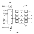
- FIG. 8 shows one embodiment of the complete architecture of the present invention, in the context of a 1-of-3 N-NARY circuit.
- an N-NARY circuit that includes the necessary components for scan is referred to as a “scan gate.”
- scan gates In normal operation, all scan gates function as normal N-NARY gates, receiving input signals, performing their logic function, and providing output signals that become inputs for the next gate.
- All Phase 0 gates are selected to be scan gates, however, those skilled in the art will appreciate that the scan architecture and techniques disclosed herein could be practiced using other phase gates as scan gates without departing from the present invention.
- scan gate 500 includes logic tree 502 that performs a logic function on its two 1-of-3 input signals, A and B, to produce a 1-of-3 N-NARY output signal, Z.
- Precharge circuit 32 and evaluate circuit 36 couple to N-NARY logic tree 502 .
- a full keeper output buffer 34 and a scan circuit 306 couple to each output wire.
- Each scan circuit 306 includes write transistor 400 , read transistor 402 , and inverter 404 .
- Each scan circuit 306 connects to a separate scan data line 412 a , 412 b , and 412 c , each of which connects through a read/write driver 414 to the scan register 416 in an arrangement similar to commonly-known RAM architecture.
- scan data lines 412 a , 412 b , and 412 c also connect to the output wires of other scan gates in other rows on a device that employs the present invention scan architecture and methodology.
- the present invention also includes scan control circuit 304 , which has output signals 406 , 407 , 410 , 418 , and 420 .
- Scan Enable (SEN) signal 420 is asserted when the system is in scan mode to control the timing of the scan gates, as explained in more detail below.
- Write signal 406 is asserted when the system is in scan mode and the wires of the output signal Z are to be forced to the value in the scan register 416 .
- Read signal 410 is asserted when the system is in scan mode and the value on each wire of the output signal Z is to be loaded into the scan register 416 , which can then be scanned out in serial fashion.
- Reset signal 407 is asserted during the reset sequence to reset the circuit for normal operation, as described in further detail below.
- Scan Precharge signal 418 is asserted to precharge the scan gates for writing during scan.
- the voltage on the scan data lines 412 is inverted by inverters 404 , and the value of the evaluate node E 0 is forced to the inverted value on the scan data line 412 a , the value of E 1 is forced to the inverted value on 412 b , and the value of E 2 is forced to the inverted value on 412 c .
- These inverted values are then inverted once again in output buffers 34 , and the values of Z 0 , Z 1 , and Z 2 are forced to the values in the scan register.
- the write transistor 400 in the scan circuit 306 coupled to output wire Z 2 is driven by the Write-or-Reset (WOR) signal 408 , while all other write transistors 400 in the other scan circuits 306 are driven by the Write signal 406 .
- the WOR signal 408 is generated by OR'ing the Write signal 406 with the Reset signal 407 .
- the scan circuit 306 that accepts the WOR signal 408 behaves like the other scan circuits 306 , as described above.
- the reset signal 407 when the reset signal 407 is asserted and neither the write signal 406 nor the read signal 410 is asserted, only the write transistor 400 in the scan circuit 306 that accepts the WOR signal 408 will conduct.
- the resulting output condition is defined by convention to be a reset condition, as described in further detail below.
- the present invention requires that one and only one output wire of the N-NARY output signal of a scan gate must couple to a scan circuit 306 that includes a write transistor 400 that is driven by the WOR signal 408 rather than the Write signal 406 .
- the output lines of each scan gate are forced to a predetermined reset condition.
- the system is reset by forcing Z 0 and Z 1 , low and Z 2 high. This is accomplished by first precharging the evaluate nodes E 0 , E 1 , and E 2 , and then asserting the WOR signal 408 , which pulls E 2 low.
- the output buffers 34 then invert the state of the evaluate nodes, and the resulting condition is Z 0 and Z 1 low and Z 2 high.
- the system is reset.
- FIG. 9 shows a network 560 of N-NARY gates, much like FIG. 4, except that in FIG. 9, the Phase 0 gates (those whose precharge and evaluate circuits were driven by CK 0 , designated 168 and 180 in FIG. 4) are now designated as scan gates 568 and 580 .
- gates 568 and 580 are scan gates in network 560 and thus include the extra scan-related components and circuitry on their output lines as shown in FIG. 8 .
- the precharge and evaluate clocks must be separately controlled. Therefore, the clock signal CK 0 to gates 168 and 180 in FIG. 4 has been replaced with two signals, CK(P) and CK(E) in FIG. 9 .
- CK(P) and CK(E) are identical to CK 0
- the scan related circuitry is quiescent, and the network 560 behaves the same as network 160 in FIG. 4 .
- FIG. 10 illustrates the relationships between the various clock signals when a network of logic that is clocked using a six-phase logic synchronization methodology is placed into scan mode to scan the output state of the scan gates.
- FIG. 10 and the following text demonstrate how the output state of each scan gate can be captured when the network is running at operating speed. As noted above, the ability to capture the output state of gates that are running at operating speed is an important performance improvement over existing scan methods and architectures.
- FIG. 10 shows the global clock signal, CLK, at the top, followed by the six sequentially generated overlapping clock signals CK 0 through CK 5 that synchronize the propagation of signals through the networked logic gates.
- CK 4 , CK 5 , and CK 0 are triggered from the falling edge of CLK
- CK 1 , CK 2 , and CK 3 are triggered from the rising edge of CLK.
- CK(P) and CK(E) the two signals at the bottom of FIG. 10, start out identical to CK 0 .
- FIG. 10 shows four full Phase 0 clock cycles, designated as 602 , 604 , 606 , and 608 .
- the “capture” cycle in the sequence depicted in FIG. 10 is cycle 606 .
- SEN is a global Scan Enable signal that is distributed through a series of latches or static registers that fan out over the design.
- the final level of SEN arrives at the input to the clock generation logic of all the scan gates in the design.
- SEN is asserted 610 at this input when the Phase 1 clock goes low 609 , shortly after the master clock CLK falls 612 but before CK 0 goes high at 614 .
- the next Phase 0 high time, ( 616 in FIG. 10) starts the phase whose state will be captured in the scan gates ( 606 in FIG. 10 ).
- SENP is latched from SEN by CK 1 going high at 618 . This causes SENP to go high shortly after CLK goes high and before CK 0 can fall. SENP is OR'ed with CK 0 to produce CK(P). Therefore, when SENP goes high, CK(P) is already high because CK 0 is high. However, when CK 0 falls at 620 , CK(P) remains high, because SENP is high.
- SENE is latched from SENP by CK 1 going low at 622 . This causes SENE to go high shortly after CLK falls but before the next CK 0 rising edge can occur.
- the inverse of SENE is ANDed with CK 0 to produce CK(E).
- CK(E) is high when CK 0 is high and SENE is low.
- SENE is latched high at 624 , CK(E) is prevented from rising again by the inverse of SENE.
- each Phase 0 scan gate is “frozen.”
- SEN, SENE, and SENP are all asserted.
- the scan gates precharged and evaluated in the prior phase, but are prevented from precharging and evaluating again because CK(P) is latched high and CK(E) is latched low. The value on each output line of each scan gate is thus available for scan.
- CLK To scan the scan gates, CLK must be stopped when it is low. Stopping CLK at 626 , shortly before it rises, puts the Phase 1 , 2 , and 3 gates in precharge and provides a quiet electrical environment for scan reading and writing.
- the scan registers can be read and the state of the scan gate outputs can be determined. Additionally, if desired, the state of the scan gate outputs can be modified by writing to the scan gates from the scan registers.
- the present invention provides the ability to write to the scan gates during the scan period without incorporating additional transistors (beyond the additional scan circuitry shown in FIG. 8) into the scan gates' structure.
- the scan gates are first precharged and then conditionally discharged via the scan write transistors 400 . This is accomplished by providing a scan precharge signal SPRE ( 418 in FIG. 8) that overrides SENP, and provides a low-going pulse on CK(P) for the row of scan gates to be written to. (Recall that SENP is ordinarily high during scan periods, keeping CK(P) high and preventing the scan gates from precharging normally.)
- the CLK can be restarted. To continue at operating speeds, CLK must be ramped up over a number of cycles, this time to avoid source the creation of undesired speed paths due to large di/dt.
- CLK When CLK is started again, the Phase 1 - 5 clocks will resume toggling, and the state of the Phase 0 scan gates (whether they have been modified by writing to them during scan or not) will propagate through the Phase 1 - 5 gates.
- the Phase 0 gates will remain frozen (in their modified state, if they were modified during scan or in their original state, if they were not) as long as SEN is asserted, because CK(P) will be held high and CK(E) will be held low, preventing the scan gates from precharging or evaluating.
- SEN is deasserted. This causes SENP to fall when CK 1 rises due to the rise of CLK. Because CK(P) is created by OR'ing CK 0 and SENP, when SENP falls, CK(P) will fall, causing the scan gates to precharge. Similarly, after SEN is deasserted, SENE will fall after the next CK 1 falling edge, shortly after the master clock CLK falls. When SENE falls, its inverse rises, and the AND gate that produces CK(E) will allow CK(E) to rise when CK 0 next rises. At this point, CK(P) and CK(E) are re-synchronized with CK 0 , and the Phase 0 scan gates return to normal operation, precharging and evaluating every clock cycle.
- FIG. 11 illustrates the relationships between the various clock signals when “stepping through” operations, as might occur when the scan gates are read or written to at each step. This single-step mode of operation is most useful for examining or troubleshooting specific areas in the logic, and for loading and executing test vectors. In this mode, the master clock CLK toggles very slowly and irregularly. For convenience only, FIG. 11 shows CLK and its various derivative clocks as symmetrical, but in reality, the shaded region (where CLK is low during scan) will be a much longer period of time than other parts of the waveform.
- SEN is toggled every clock cycle.
- SEN goes high at the input to the scan gates' clock generation logic when the Phase 1 clock goes low at 709 , shortly after the master clock CLK falls 712 but before CK 0 goes high at 714 .
- SENP is latched from SEN by CK 1 going high at 718 . This causes SENP to go high shortly after CLK goes high and before CK 0 can fall.
- CK(P) is already high because CK 0 is high.
- CK(P) remains high, because SENP (which, as the reader will recall from the previous discussion, is OR'ed with CK 0 to produce CK(P)) is high.
- SENE is latched from SENP by CK 1 going low at 722 . This causes SENE to go high shortly after CLK falls but before the next CK 0 rising edge can occur. Because the inverse of SENE is ANDed with CK 0 to produce CK(E), CK(E) is high when CK 0 is high and SENE is low. When SENE is latched high at 724 , CK(E) is prevented from rising again by the inverse of SENE.
- Reading and optional writing of the state of the scan gates can now occur (the shaded regions 730 on FIG. 11 ). As discussed above, the duration of the scan periods 730 will be much longer than implied by the clock signals depicted in FIG. 11 . In single step operation, during the scan periods 730 , the clock is either stopped completely or is running very slowly to provide sufficient time to read the scan registers or load test vectors.
- SEN is deasserted at 732 , just after the Phase 1 clock goes low at 722 , but prior to the first shaded scan period 730 .
- SENE and SENP stay high during the scan period (recall that SENP is latched by a Phase 1 high clock, and SENE is latched from SENP.
- CLK is stopped during the scan period 730 , CK 1 stays low. Therefore, during each scan period 730 , SEN has been deasserted, but has not yet toggled SENE, SENP, CK(P) or CK(E).
- CLK can be restarted or stepped to the next cycle.
- CLK goes high, causing CK 0 , CK 1 , and SENP SENE, CK(P) and CK(E) to toggle as shown in FIG. 11 and as described above in connection with full-speed operation.
- SEN is again asserted, and the process repeats again as shown in FIG. 11 . Therefore, in single step or slow clock operation, scan gates can be read or written to every second clock cycle. This allows logic to propagate from a Phase 0 gate through the rest of the gates before the next scan cycle.
- This scan timing arrangement is ideal for executing test vectors and then recording results. This is accomplished by reading a scan gate's output state during a scan period 730 and then writing an input vector to the gate. The clock is then restarted, and the vector propagates state through the Phase 1 - 5 gates to the next Phase 0 scan gate. The clock is then stopped for the next scan period, and the output state of that gate read and compared to the expected result.
- FIG. 12 shows an alternative embodiment of scan gate 500 , designated 800 .
- FIG. 12 is similar to FIG. 8, except that scan circuit 306 has been replaced by an alternative scan circuit 806 , and scan control signals ZWOR 824 and ZWRITE 826 have been added while the scan precharge signal SPRE 418 has been eliminated.
- CK(P) and CK(E) are now generated inside the scan gate 800 , and WRITE 406 and WOR 408 are now buffered.
- scan circuit 806 includes three NFET transistors 810 , 816 , and 818 , and two PFET transistors 812 and 814 .
- read signal 410 When the read signal 410 is high, read transistor 810 conducts and the state of the output signals Z 0 , Z 1 , and Z 2 is provided to the scan register 416 through scan data lines 412 a , 412 b , and 412 c.
- one and only one output line of an N-NARY scan gate 800 is connected to a scan circuit 806 wherein the gate of the write transistors couples to the write-or-reset signal WOR 408 .
- WOR 408 has an inverse, ZWOR 824 .
- FIG. 12 shows clock signals CK(P) as an input to the precharge circuit 32
- CK(E) as an input to the evaluate circuit 36
- scan gate 800 has only a single clock input, CKS, that is the same as CK 3 , which is basically an inverted version of CK 0 , as shown in FIGS. 10 and 11.
- CKS enters scan gate 800 and is inverted to precharge the logic tree 502 .
- CKS is also NOR'ed together with SEN 420 to produce CK(E).
- this clock scheme functions just like the clocking arrangement described in conjunction with the scan architecture shown in FIG. 8 and the clock signals shown in FIGS. 10 and 11, except that in this clocking arrangement, neither SENE nor SENP are needed or generated.
- FIG. 13 shows two scan gates embedded in a network of dynamic logic.
- FIG. 13 is similar to FIG. 9, except that in FIG. 13, network 860 includes scan gates 868 and 880 , which are implemented in the alternative embodiment 800 shown in FIG. 12 . Accordingly, the clock inputs to the scan gates (CK(P) and CK(E) in FIG. 9) have been replaced by CKS.
- the architecture and clocking arrangement shown in FIG. 12 has some advantages over that shown in FIG. 8 .
- the scan gate clock generation is simpler. This provides layout and floorplanning advantages.
- decoupling the scan logic from the Phase 0 clock generation sites facilitates the use of 64-bit virtual scan rows, which may comprise less than one or more than several physical rows, depending upon the scannable bit population of each physical row.
- the distribution of SEN over the design no longer needs to be synchronous and high-speed.
- FIG. 12 only allows for the at-speed capture of the state of the scan gates if the design can tolerate the power supply overshoot caused by a high negative di/dt.
- CK(P) will continue to toggle as long as CKS toggles. Therefore, to capture a certain output state, CKS must be stopped abruptly to prevent CK(P) from precharging the logic tree and destroying the output state of the scan gate.
- FIG. 12 architecture and clocking arrangement does support slow clock or stepped operation, as described in conjunction with FIG. 11, although the behavior of CK(E) is slightly different, as shown in FIG. 14 .
- FIG. 14 depicts the operation of the clocks relative to each other during stepped operation scan using the scan architecture shown in FIG. 12 .
- the duration of the scan periods 730 will be much longer than implied by the clock signals depicted in FIG. 14 .
- the clock is either stopped completely or is running very slowly to provide sufficient time to read the scan registers or load test vectors.
- the scan periods 730 occur every second clock cycle, when the master clock and the Phase 1 , 2 , and 3 are low, thus providing a quiet electrical environment for reading and writing to the scan gates.
- CLK and the Phase 1 - 5 clocks are identical to the CLK and Phase 1 - 5 clocks shown and described in FIG. 11 .
- the “Phase 0 ” reference clock shown in FIG. 11 has been replaced, in FIG. 13, with the CKS signal that is the clock signal input to the scan gate 800 .
- FIG. 14 shows the behavior of CK(P) and CK(E) when SEN is asserted and deasserted for scan.
- CK(P) is an inverted version of CKS, and continues to toggle as CKS toggles.
- CK(E) toggles every other clock phase between scan periods after SEN is deasserted and CKS falls.
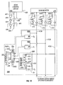
- FIG. 15 shows another embodiment of scan gate, designated 900 , along with the same scan control circuit 304 , scan register 416 , and read/write drivers 414 shown and described previously.
- FIG. 15 also shows the master clock generation circuit 906 that generates the master clock signal, CLK, which is provided to the clock spine 902 .
- scan control circuit 304 provides SEN 420 to the master clock generation circuit 906 and WOR 408 to the clock spine 902 .
- Local clock generation circuit 904 receives CLK from the clock spine 902 and generates the sequentially generated logic clock signals CK 0 through CK 5 .
- the local clock generation circuit 904 also receives WOR 408 from the clock spine, which controls the operation of some of the sequentially generated logic clock signals during the write process, as explained in further detail below.
- the scan gate 900 shown in FIG. 15 is identical to scan gate 800 shown in FIG. 12, except that in this embodiment, the clock input to scan gate 900 is one of the sequentially generated logic clock signals generated by the clock generation circuit 904 that is used to time and synchronize all the logic circuitry in the design, rather than a special clock signal generated solely for scan.
- the logic clock signal input is CK 0 .
- designers could designate gates other than phase 0 gates as scan gates without departing from the present invention. For example, a designer could designate some or all of the phase 3 gates—gates that receive the CK 3 logic clock signal—as scan gates, rather than the phase 0 gates as described herein.
- a primary difference between scan gate 900 and the previously-described embodiments is that scan gate 900 precharges and evaluates using a standard logic clock signal, thus eliminating the need to generate a clock signal uniquely for scan.
- Scan gate 900 includes the same scan circuits 806 as described in the previous embodiment, and therefore, like scan gate 800 , scan gate 900 does not need to be precharged before writing to it in scan mode.
- the logic synchronization clock scheme can be implemented so as to further eliminate any need to precharge scan gate 900 for scan writing.
- scan gate 900 has only a standard single clock input, CK 0 , which is generated by the local clock generation circuit 904 .
- Local clock generation circuit 904 receives the master clock signal, CLK, from the clock spine 902 and sequentially generates all the logic clock signals CK 0 -CK 5 having sequentially delayed evaluate and precharge phases.
- CLK master clock signal
- CK 0 enters the scan gate 900 from the clock generation circuit 904 and precharges the logic tree 502 when it is low and evaluates the logic tree 502 when it toggles high.
- the local clock generation circuit 904 generates the sequentially generated logic clock signals by buffering and delaying CLK.
- CK 0 , CK 1 , and CK 2 transition with CLK's edge, sequentially delayed in the order listed.
- CK 3 , CK 4 , and CK 5 transition opposite CLK's edges, again sequentially delayed in the order listed.
- the arrangement and behavior of the sequentially generated logic clock signals during regular operation and during scan modes is shown and described below, in connection with FIGS. 16 and 17.
- SEN 420 is asserted and stops CLK high. After sequential delays, CK 0 , CK 1 , and CK 2 will be stopped high, while CK 3 , CK 4 , and CK 5 will be stopped low. To write to the scan gates, all logic clock signal inputs to gates “downstream” of the scan gates that are high when CLK is stopped must be forced low, to force these downstream gates into a precharge mode.
- a common approach to circuit testing using scan is to stop the clock, write a test vector to one or more scan gates, start the clock and let the test vector propagate through the logic to the next downstream scan gate, stop the clock again, read the output state of the downstream scan gate, and compare it with the expected output state, given the value of the input test vector and the functionality of the gates between the two scan gates.
- the output at the downstream scan gate on the next read may not conform to expected results, implying a circuit error where none may exist.
- WRITE 406 is asserted, causing WOR 408 to go high, and ZWRITE 826 and ZWOR 824 to go low.
- WOR 408 forces CK 1 and CK 2 low to clear out stale information in downstream gates along the datapath. While CLK is stopped, CK 1 and CK 2 need not be controlled with standard clock signal precision; all that is required is that they be low during the write process and then returned to high after the write, to correctly pass data after CLK is restarted.
- Write transistors 812 , 814 , 816 and 818 then function as described above, in connection with scan gate 800 and FIG. 12, and the write proceeds.
- any of the output wires Z 0 , Z 1 , or Z 2 is to be forced low, then the value on the corresponding scan data line 412 a , 412 b , or 412 c will be low, transistor 812 will be turned on, and transistor 818 will be off. Transistor 812 will discharge through transistor 814 to the evaluate node and the output buffer 34 will invert the high value such that the value on the output line is low.
- phase 0 scan gate is to be read instead of written to, there is no need to force CK 1 and CK 2 low. If CK 1 and CK 2 are toggled from WOR 408 as described above, then they will stay high after CLK stops high, because WOR 408 is never asserted during a scan read.
- SEN 420 is asserted and stops CLK high, which stops CK 0 high.
- READ 410 is asserted, read transistor 810 conducts and the state of the output signals Z 0 , Z 1 , and Z 2 is provided to the scan register 416 through scan data lines 412 a , 412 b , and 412 c.
- FIG. 16 illustrates the relationships between the sequentially generated logic clock signals during a scan write using this embodiment of scan gate 900 and a six-phase logic synchronization methodology where the phase 0 gates are the scan gates.
- FIG. 16 shows the global clock signal, CLK, followed by the six sequentially generated overlapping clock signals CK 0 through CK 5 that synchronize the propagation of signals through the networked logic gates via the clock spine.
- CLK global clock signal
- CK 0 , CK 1 , and CK 2 fall after CLK falls
- CK 3 , CK 4 , and CK 5 rise after CLK falls.
- the network of synchronously clocked precharge logic gates is assumed to be originally in normal, at speed operation.
- SEN is the global Scan Enable signal that is distributed through a series of latches or static registers that fan out over the design.
- SEN is asserted 958 . This causes CLK to stop after its next rising edge, shown on FIG. 16 at 959 , which also stops all the sequentially generated logic clocks.
- the WRITE signal is then asserted at 962 , which asserts the WOR signal at 964 , which in turn forces CK 1 and CK 2 low at 966 and 968 , respectively.
- the write proceeds as described above, after which WRITE is deasserted at 970 , deasserting WOR at 972 and toggling CK 1 and CK 2 high at 974 and 976 , respectively.
- SEN is deasserted at 980 to restart CLK.
- CLK falls at 982 , the sequentially generated local clocks then resume toggling in accordance with the failing edge of CLK, and normal operation ensues.
- FIG. 17 The relationship of the clock signals during the read process is shown in FIG. 17 .
- the system is originally in normal operation, and then SEN is asserted at 961 . Thereafter, CLK stops after its next rising edge, shown on FIG. 17 at 963 . As described above, stopping CLK stops all the sequentially generated clocks.
- READ is asserted at 965 , the read proceeds as described above, and READ is then deasserted at 967 .
- SEN is deasserted at 971 to restart CLK, and again, the sequentially generated logic clock signals resume toggling in normal operation upon the falling edge of CLK at 973 .
- FIG. 18 shows two scan gates embedded in a network of dynamic logic.
- FIG. 18 is similar to FIGS. 9 and 13, except that in FIG. 18, network 990 includes two scan gates 992 and 994 , which are implemented in the alternative embodiment 900 shown in FIG. 15 . Accordingly, the clock inputs to the scan gates (CK(P) and CK(E) in FIG. 9, and CKs in FIG. 13) have been replaced by CK 0 .
- this embodiment is used in a sequentially clocked precharge logic network that cannot tolerate abruptly stopping the clocks when the logic is running at speed, the clocks can be slowed or stepped, and then stopped as described above when the user is ready to capture the output state of the scan gates or write to the scan gates, without creating a problem.
- the present invention comprises a method and apparatus for scan of dynamic or N-NARY clocked precharge logic circuits that include a logic tree with one or more evaluate nodes, a precharge circuit, an evaluate circuit, one or more output buffers, and one or more scan circuits, where the logic circuit receives one or more input signals and a clock signal having an evaluate phase and a precharge phase, and produces one or more output signals.
- the present invention includes a scan control circuit that generates scan control signals including a scan enable signal, one or more scan registers, and one or more read/write drivers coupled to the scan control circuit, the scan register, and the output buffers such that when the scan circuit receives scan control signals, the state of the output signal is provided to the scan register, or alternatively, the state of the output signal can be forced to a state specified by information in the scan register.
- the present invention further comprises a network of multiple sequentially clocked precharge logic gates, wherein the input signals of a gate that receives a particular sequentially generated logic clock signal couple to a first sequentially clocked precharge logic gate that receives the immediately preceding sequentially generated logic clock signal, and the output signals of the gate that receives the particular sequentially generated logic clock signal couple to a second sequentially clocked precharge logic gate that receives the immediately following sequentially generated logic clock signal.
- the sequentially generated logic clock signals are each one of at least 3 logic clock signals sequentially generated by a clock generation circuit coupled to a clock spine.
- the sequentially generated logic clock signals are generated with a sequential delay, such that the evaluate phase of a particular logic clock signal overlaps the evaluate phase of the immediately preceding logic clock signal by approximately the same amount of time that the evaluate phase of the particular logic clock signal phase overlaps the evaluate phase of the immediately following logic clock signal.
- the present invention further comprises reading the output state generated by the logic circuit by generating a scan enable signal and a read signal, stopping the logic circuit's clock signal during the evaluate phase, providing the read signal to the scan circuits and the read/write drivers coupled to the scan circuits and to a scan register.
- the present invention includes forcing the output state of a scannable logic circuit that receives a first sequentially generated logic clock signal to a user-selected state, by loading the scan register with the user-selected output state, generating a scan enable signal and one or more write signals, stopping the sequentially generated logic clock signals when the first sequentially generated logic clock signal is in the evaluate phase, forcing all sequentially generated logic clock signals received by gates downstream of the scannable logic circuit to the precharge phase if they were in the evaluate phase when the clocks were stopped, providing the write signals to the scan circuits and to one or more of the read/write drivers, returning the sequentially generated logic clock signals to the evaluate phase if they were forced to the precharge phase, and restarting all clocks.
Abstract
Description
Claims (16)
Priority Applications (1)
| Application Number | Priority Date | Filing Date | Title |
|---|---|---|---|
| US09/901,411 US6745357B2 (en) | 1998-10-27 | 2001-07-09 | Dynamic logic scan gate method and apparatus |
Applications Claiming Priority (3)
| Application Number | Priority Date | Filing Date | Title |
|---|---|---|---|
| US09/179,330 US6118304A (en) | 1997-11-20 | 1998-10-27 | Method and apparatus for logic synchronization |
| US09/468,759 US6415405B1 (en) | 1998-10-27 | 1999-12-21 | Method and apparatus for scan of synchronized dynamic logic using embedded scan gates |
| US09/901,411 US6745357B2 (en) | 1998-10-27 | 2001-07-09 | Dynamic logic scan gate method and apparatus |
Related Parent Applications (1)
| Application Number | Title | Priority Date | Filing Date |
|---|---|---|---|
| US09/468,759 Continuation-In-Part US6415405B1 (en) | 1998-10-27 | 1999-12-21 | Method and apparatus for scan of synchronized dynamic logic using embedded scan gates |
Publications (2)
| Publication Number | Publication Date |
|---|---|
| US20010039635A1 US20010039635A1 (en) | 2001-11-08 |
| US6745357B2 true US6745357B2 (en) | 2004-06-01 |
Family
ID=26875227
Family Applications (1)
| Application Number | Title | Priority Date | Filing Date |
|---|---|---|---|
| US09/901,411 Expired - Lifetime US6745357B2 (en) | 1998-10-27 | 2001-07-09 | Dynamic logic scan gate method and apparatus |
Country Status (1)
| Country | Link |
|---|---|
| US (1) | US6745357B2 (en) |
Cited By (4)
| Publication number | Priority date | Publication date | Assignee | Title |
|---|---|---|---|---|
| US20030163752A1 (en) * | 2002-02-22 | 2003-08-28 | Sanyo Electric Co., Ltd. | Control method and circuit for stopping clock signal |
| US20040150660A1 (en) * | 2003-01-09 | 2004-08-05 | Canon Kabushiki Kaisha | Drive control apparatus and method for matrix panel |
| US20040153806A1 (en) * | 2002-09-17 | 2004-08-05 | Yukio Sugimura | Technique for testability of semiconductor integrated circuit |
| US20080222471A1 (en) * | 2007-03-08 | 2008-09-11 | Chinsong Sul | Circuitry to prevent peak power problems during scan shift |
Families Citing this family (2)
| Publication number | Priority date | Publication date | Assignee | Title |
|---|---|---|---|---|
| JP2021082879A (en) * | 2019-11-15 | 2021-05-27 | 富士電機株式会社 | Logic circuit and circuit chip |
| US20240015419A1 (en) * | 2022-07-11 | 2024-01-11 | Mellanox Technologies, Ltd. | Synchronization of optically switched networks |
Citations (31)
| Publication number | Priority date | Publication date | Assignee | Title |
|---|---|---|---|---|
| US4860322A (en) | 1988-10-05 | 1989-08-22 | Intel Corporation | Anti-clock skew distribution apparatus |
| US5041742A (en) | 1990-05-09 | 1991-08-20 | Motorola, Inc. | Structured scan path circuit for incorporating domino logic |
| US5120988A (en) | 1987-08-28 | 1992-06-09 | Kabushiki Kaisha Toshiba | Clock generator circuit providing reduced current consumption |
| US5122679A (en) | 1988-10-14 | 1992-06-16 | Hitachi, Ltd. | Integrated logic circuit with clock skew adjusters |
| US5124572A (en) | 1990-11-27 | 1992-06-23 | Hewlett-Packard Co. | VLSI clocking system using both overlapping and non-overlapping clocks |
| US5306962A (en) | 1990-11-27 | 1994-04-26 | Hewlett-Packard Company | Qualified non-overlapping clock generator to provide control lines with non-overlapping clock timing |
| US5410686A (en) | 1993-11-01 | 1995-04-25 | Motorola, Inc. | Methods for scan path debugging |
| US5434520A (en) | 1991-04-12 | 1995-07-18 | Hewlett-Packard Company | Clocking systems and methods for pipelined self-timed dynamic logic circuits |
| US5450455A (en) | 1993-06-28 | 1995-09-12 | Tandem Computers Incorporated | Method and apparatus for including the states of nonscannable parts in a scan chain |
| US5517136A (en) | 1995-03-03 | 1996-05-14 | Intel Corporation | Opportunistic time-borrowing domino logic |
| US5760610A (en) | 1996-03-01 | 1998-06-02 | Hewlett-Packard Company | Qualified universal clock buffer circuit for generating high gain, low skew local clock signals |
| US5764092A (en) | 1995-05-26 | 1998-06-09 | Nec | Delay clock generator for generating a plurality of delay clocks delaying the basic clock |
| US5774007A (en) | 1995-10-17 | 1998-06-30 | Sony Corporation | Clock distributing apparatus having V/I and I/V converters |
| US5774511A (en) | 1996-04-19 | 1998-06-30 | International Business Machines Corporation | Processor clock circuit |
| US5841670A (en) * | 1994-03-09 | 1998-11-24 | Texas Instruments Incorporated | Emulation devices, systems and methods with distributed control of clock domains |
| US5870411A (en) | 1996-12-13 | 1999-02-09 | International Business Machines Corporation | Method and system for testing self-timed circuitry |
| US5880609A (en) | 1997-01-23 | 1999-03-09 | Sun Microsystems, Inc. | Non-blocking multiple phase clocking scheme for dynamic logic |
| US5886540A (en) | 1996-05-31 | 1999-03-23 | Hewlett-Packard Company | Evaluation phase expansion for dynamic logic circuits |
| US5896046A (en) | 1997-01-27 | 1999-04-20 | International Business Machines Corporation | Latch structure for ripple domino logic |
| US5917331A (en) | 1995-10-23 | 1999-06-29 | Megatest Corporation | Integrated circuit test method and structure |
| US5923188A (en) | 1995-06-14 | 1999-07-13 | Nec Corporation | Clock signal distribution circuit of tree structure with minimized skew |
| US5952861A (en) | 1997-06-19 | 1999-09-14 | Sun Microsystems, Inc. | Dynamic pulse register with scan functionality |
| US5951702A (en) | 1997-04-04 | 1999-09-14 | S3 Incorporated | RAM-like test structure superimposed over rows of macrocells with added differential pass transistors in a CPU |
| US5978944A (en) * | 1997-11-26 | 1999-11-02 | Intel Corporation | Method and apparatus for scan testing dynamic circuits |
| US5983013A (en) | 1997-06-30 | 1999-11-09 | Sun Microsystems, Inc. | Method for generating non-blocking delayed clocking signals for domino logic |
| US6006347A (en) * | 1997-09-17 | 1999-12-21 | Cypress Semiconductor Corporation | Test mode features for synchronous pipelined memories |
| US6018254A (en) | 1997-06-30 | 2000-01-25 | Sun Microsystems, Inc. | Non-blocking delayed clocking system for domino logic |
| US6100734A (en) | 1994-11-30 | 2000-08-08 | Unisys Corporation | IC chip using a phase-locked loop for providing signals having different timing edges |
| US6158032A (en) | 1998-03-27 | 2000-12-05 | International Business Machines Corporation | Data processing system, circuit arrangement and program product including multi-path scan interface and methods thereof |
| US6185691B1 (en) | 1997-12-29 | 2001-02-06 | Intel Corporation | Clock generation |
| US6242269B1 (en) * | 1997-11-03 | 2001-06-05 | Texas Instruments Incorporated | Parallel scan distributors and collectors and process of testing integrated circuits |
-
2001
- 2001-07-09 US US09/901,411 patent/US6745357B2/en not_active Expired - Lifetime
Patent Citations (32)
| Publication number | Priority date | Publication date | Assignee | Title |
|---|---|---|---|---|
| US5120988A (en) | 1987-08-28 | 1992-06-09 | Kabushiki Kaisha Toshiba | Clock generator circuit providing reduced current consumption |
| US4860322A (en) | 1988-10-05 | 1989-08-22 | Intel Corporation | Anti-clock skew distribution apparatus |
| US5122679A (en) | 1988-10-14 | 1992-06-16 | Hitachi, Ltd. | Integrated logic circuit with clock skew adjusters |
| US5041742A (en) | 1990-05-09 | 1991-08-20 | Motorola, Inc. | Structured scan path circuit for incorporating domino logic |
| US5041742B1 (en) | 1990-05-09 | 1992-08-18 | Carbonaro Joseph | |
| US5124572A (en) | 1990-11-27 | 1992-06-23 | Hewlett-Packard Co. | VLSI clocking system using both overlapping and non-overlapping clocks |
| US5306962A (en) | 1990-11-27 | 1994-04-26 | Hewlett-Packard Company | Qualified non-overlapping clock generator to provide control lines with non-overlapping clock timing |
| US5434520A (en) | 1991-04-12 | 1995-07-18 | Hewlett-Packard Company | Clocking systems and methods for pipelined self-timed dynamic logic circuits |
| US5450455A (en) | 1993-06-28 | 1995-09-12 | Tandem Computers Incorporated | Method and apparatus for including the states of nonscannable parts in a scan chain |
| US5410686A (en) | 1993-11-01 | 1995-04-25 | Motorola, Inc. | Methods for scan path debugging |
| US5841670A (en) * | 1994-03-09 | 1998-11-24 | Texas Instruments Incorporated | Emulation devices, systems and methods with distributed control of clock domains |
| US6100734A (en) | 1994-11-30 | 2000-08-08 | Unisys Corporation | IC chip using a phase-locked loop for providing signals having different timing edges |
| US5517136A (en) | 1995-03-03 | 1996-05-14 | Intel Corporation | Opportunistic time-borrowing domino logic |
| US5764092A (en) | 1995-05-26 | 1998-06-09 | Nec | Delay clock generator for generating a plurality of delay clocks delaying the basic clock |
| US5923188A (en) | 1995-06-14 | 1999-07-13 | Nec Corporation | Clock signal distribution circuit of tree structure with minimized skew |
| US5774007A (en) | 1995-10-17 | 1998-06-30 | Sony Corporation | Clock distributing apparatus having V/I and I/V converters |
| US5917331A (en) | 1995-10-23 | 1999-06-29 | Megatest Corporation | Integrated circuit test method and structure |
| US5760610A (en) | 1996-03-01 | 1998-06-02 | Hewlett-Packard Company | Qualified universal clock buffer circuit for generating high gain, low skew local clock signals |
| US5774511A (en) | 1996-04-19 | 1998-06-30 | International Business Machines Corporation | Processor clock circuit |
| US5886540A (en) | 1996-05-31 | 1999-03-23 | Hewlett-Packard Company | Evaluation phase expansion for dynamic logic circuits |
| US5870411A (en) | 1996-12-13 | 1999-02-09 | International Business Machines Corporation | Method and system for testing self-timed circuitry |
| US5880609A (en) | 1997-01-23 | 1999-03-09 | Sun Microsystems, Inc. | Non-blocking multiple phase clocking scheme for dynamic logic |
| US5896046A (en) | 1997-01-27 | 1999-04-20 | International Business Machines Corporation | Latch structure for ripple domino logic |
| US5951702A (en) | 1997-04-04 | 1999-09-14 | S3 Incorporated | RAM-like test structure superimposed over rows of macrocells with added differential pass transistors in a CPU |
| US5952861A (en) | 1997-06-19 | 1999-09-14 | Sun Microsystems, Inc. | Dynamic pulse register with scan functionality |
| US5983013A (en) | 1997-06-30 | 1999-11-09 | Sun Microsystems, Inc. | Method for generating non-blocking delayed clocking signals for domino logic |
| US6018254A (en) | 1997-06-30 | 2000-01-25 | Sun Microsystems, Inc. | Non-blocking delayed clocking system for domino logic |
| US6006347A (en) * | 1997-09-17 | 1999-12-21 | Cypress Semiconductor Corporation | Test mode features for synchronous pipelined memories |
| US6242269B1 (en) * | 1997-11-03 | 2001-06-05 | Texas Instruments Incorporated | Parallel scan distributors and collectors and process of testing integrated circuits |
| US5978944A (en) * | 1997-11-26 | 1999-11-02 | Intel Corporation | Method and apparatus for scan testing dynamic circuits |
| US6185691B1 (en) | 1997-12-29 | 2001-02-06 | Intel Corporation | Clock generation |
| US6158032A (en) | 1998-03-27 | 2000-12-05 | International Business Machines Corporation | Data processing system, circuit arrangement and program product including multi-path scan interface and methods thereof |
Non-Patent Citations (2)
| Title |
|---|
| Harris, Skew-Tolerant Domino Circuits, IEEE Journal of Solid-State Circuits, 11/97, p 1702-1711, vol. 32, No. 11. |
| U.S. Patent Application entitled "Method and Apparatus for Scan of Synchronized Cynamic Logic Using Embedded Scan Gates," Inventors: Horne, et al., Ser. No. 09/468,759, filed on Dec. 21, 1999. |
Cited By (8)
| Publication number | Priority date | Publication date | Assignee | Title |
|---|---|---|---|---|
| US20030163752A1 (en) * | 2002-02-22 | 2003-08-28 | Sanyo Electric Co., Ltd. | Control method and circuit for stopping clock signal |
| US7149912B2 (en) * | 2002-02-22 | 2006-12-12 | Sanyo Electric Co., Ltd. | Control method and circuit for stopping clock signal |
| US20040153806A1 (en) * | 2002-09-17 | 2004-08-05 | Yukio Sugimura | Technique for testability of semiconductor integrated circuit |
| US7168004B2 (en) * | 2002-09-17 | 2007-01-23 | Matsushita Electric Industrial Co., Ltd. | Technique for testability of semiconductor integrated circuit |
| US20040150660A1 (en) * | 2003-01-09 | 2004-08-05 | Canon Kabushiki Kaisha | Drive control apparatus and method for matrix panel |
| US7277105B2 (en) * | 2003-01-09 | 2007-10-02 | Canon Kabushiki Kaisha | Drive control apparatus and method for matrix panel |
| US20080222471A1 (en) * | 2007-03-08 | 2008-09-11 | Chinsong Sul | Circuitry to prevent peak power problems during scan shift |
| US7831877B2 (en) * | 2007-03-08 | 2010-11-09 | Silicon Image, Inc. | Circuitry to prevent peak power problems during scan shift |
Also Published As
| Publication number | Publication date |
|---|---|
| US20010039635A1 (en) | 2001-11-08 |
Similar Documents
| Publication | Publication Date | Title |
|---|---|---|
| US6108805A (en) | Domino scan architecture and domino scan flip-flop for the testing of domino and hybrid CMOS circuits | |
| US6822482B2 (en) | Dynamic scan circuitry for B-phase | |
| JP3151391B2 (en) | Local clock generation / distribution circuit for integrated circuit testing | |
| JP4099261B2 (en) | Domino logic circuit, apparatus, and method for controlling precharge based upon completion of evaluation by next domino logic stage | |
| US7000164B2 (en) | Method for scan testing and clocking dynamic domino circuits in VLSI systems using level sensitive latches and edge triggered flip flops | |
| US20050235185A1 (en) | Scan interface | |
| JPH08211133A (en) | Method and equipment for testing high-speed digital-circuit constitution element | |
| EP1168369B1 (en) | Synchronous semiconductor memory device | |
| US5951702A (en) | RAM-like test structure superimposed over rows of macrocells with added differential pass transistors in a CPU | |
| US5911063A (en) | Method and apparatus for single phase clock distribution with minimal clock skew | |
| US6853212B2 (en) | Gated scan output flip-flop | |
| US6784715B2 (en) | Conditional clock buffer circuit | |
| US5926487A (en) | High performance registers for pulsed logic | |
| US6745357B2 (en) | Dynamic logic scan gate method and apparatus | |
| US6271683B1 (en) | Dynamic logic scan gate method and apparatus | |
| US7913131B2 (en) | Scan chain cell with delay testing capability | |
| JP2003519802A (en) | Test method for circuit having three-state driver and circuit used for test | |
| US6415405B1 (en) | Method and apparatus for scan of synchronized dynamic logic using embedded scan gates | |
| KR20000069742A (en) | Single-phase domino time borrowing logic with clocks at first and last stages and latch at last stage | |
| US6292402B1 (en) | Prefetch write driver for a random access memory | |
| US6066964A (en) | Dynamic bus | |
| US6950973B2 (en) | Dynamic scan circuitry for A-phase | |
| US5926519A (en) | Semiconductor integrated circuit including dynamic registers | |
| US7137052B2 (en) | Methods and apparatus for minimizing current surges during integrated circuit testing | |
| US6453258B1 (en) | Optimized burn-in for fixed time dynamic logic circuitry |
Legal Events
| Date | Code | Title | Description |
|---|---|---|---|
| AS | Assignment |
Owner name: INTRINSITY, INC., TEXAS Free format text: ASSIGNMENT OF ASSIGNORS INTEREST;ASSIGNORS:CHRUDIMSKY, DAVID W.;HORNE, STEPHEN C.;BLOMGREN, JAMES S.;AND OTHERS;REEL/FRAME:014306/0854 Effective date: 20010628 |
|
| STCF | Information on status: patent grant |
Free format text: PATENTED CASE |
|
| FEPP | Fee payment procedure |
Free format text: PAT HOLDER NO LONGER CLAIMS SMALL ENTITY STATUS, ENTITY STATUS SET TO UNDISCOUNTED (ORIGINAL EVENT CODE: STOL); ENTITY STATUS OF PATENT OWNER: LARGE ENTITY |
|
| AS | Assignment |
Owner name: SILICON VALLEY BANK, CALIFORNIA Free format text: SECURITY AGREEMENT;ASSIGNOR:INTRINSITY, INC.;REEL/FRAME:018923/0404 Effective date: 20070101 |
|
| AS | Assignment |
Owner name: ADAMS CAPITAL MANAGEMENT III, L.P., TEXAS Free format text: SECURITY AGREEMENT;ASSIGNOR:INTRINSITY, INC.;REEL/FRAME:019161/0661 Effective date: 20070207 |
|
| FPAY | Fee payment |
Year of fee payment: 4 |
|
| AS | Assignment |
Owner name: INTRINSITY, INC., TEXAS Free format text: RELEASE OF SECURITY INTEREST;ASSIGNOR:ADAMS CAPITAL MANAGEMENT III, L.P.;REEL/FRAME:020206/0340 Effective date: 20071206 |
|
| AS | Assignment |
Owner name: PATENT SKY LLC, NEW YORK Free format text: GRANT OF SECURITY INTEREST;ASSIGNOR:INTRINSITY INC.;REEL/FRAME:020234/0365 Effective date: 20071206 |
|
| AS | Assignment |
Owner name: INTRINSITY, INC, TEXAS Free format text: RELEASE BY SECURED PARTY;ASSIGNOR:SILICON VALLEY BANK;REEL/FRAME:020525/0485 Effective date: 20080107 |
|
| AS | Assignment |
Owner name: APPLE INC.,CALIFORNIA Free format text: ASSIGNMENT OF ASSIGNORS INTEREST;ASSIGNOR:INTRINSITY, INC.;REEL/FRAME:024380/0329 Effective date: 20100401 Owner name: APPLE INC., CALIFORNIA Free format text: ASSIGNMENT OF ASSIGNORS INTEREST;ASSIGNOR:INTRINSITY, INC.;REEL/FRAME:024380/0329 Effective date: 20100401 |
|
| FPAY | Fee payment |
Year of fee payment: 8 |
|
| FPAY | Fee payment |
Year of fee payment: 12 |