US6784491B2 - MOS devices with reduced fringing capacitance - Google Patents
MOS devices with reduced fringing capacitance Download PDFInfo
- Publication number
- US6784491B2 US6784491B2 US10/256,978 US25697802A US6784491B2 US 6784491 B2 US6784491 B2 US 6784491B2 US 25697802 A US25697802 A US 25697802A US 6784491 B2 US6784491 B2 US 6784491B2
- Authority
- US
- United States
- Prior art keywords
- gate
- polysilicon layer
- layer
- arc
- area
- Prior art date
- Legal status (The legal status is an assumption and is not a legal conclusion. Google has not performed a legal analysis and makes no representation as to the accuracy of the status listed.)
- Expired - Fee Related
Links
- 229910021420 polycrystalline silicon Inorganic materials 0.000 claims abstract description 35
- 229920005591 polysilicon Polymers 0.000 claims abstract description 35
- 239000000758 substrate Substances 0.000 claims abstract description 16
- 125000006850 spacer group Chemical group 0.000 claims description 21
- 230000007423 decrease Effects 0.000 claims description 5
- 230000003247 decreasing effect Effects 0.000 claims description 5
- 238000000034 method Methods 0.000 description 25
- 238000010586 diagram Methods 0.000 description 17
- 230000015572 biosynthetic process Effects 0.000 description 12
- FVBUAEGBCNSCDD-UHFFFAOYSA-N silicide(4-) Chemical compound [Si-4] FVBUAEGBCNSCDD-UHFFFAOYSA-N 0.000 description 8
- 239000003989 dielectric material Substances 0.000 description 6
- 150000004767 nitrides Chemical class 0.000 description 6
- 238000004519 manufacturing process Methods 0.000 description 5
- 229910021332 silicide Inorganic materials 0.000 description 5
- VYPSYNLAJGMNEJ-UHFFFAOYSA-N Silicium dioxide Chemical compound O=[Si]=O VYPSYNLAJGMNEJ-UHFFFAOYSA-N 0.000 description 4
- 239000004065 semiconductor Substances 0.000 description 4
- 238000005530 etching Methods 0.000 description 3
- 239000000463 material Substances 0.000 description 3
- 229910000577 Silicon-germanium Inorganic materials 0.000 description 2
- 238000005229 chemical vapour deposition Methods 0.000 description 2
- 229910052681 coesite Inorganic materials 0.000 description 2
- 229910052906 cristobalite Inorganic materials 0.000 description 2
- 229910052751 metal Inorganic materials 0.000 description 2
- 239000002184 metal Substances 0.000 description 2
- 229910044991 metal oxide Inorganic materials 0.000 description 2
- 150000004706 metal oxides Chemical class 0.000 description 2
- 239000000377 silicon dioxide Substances 0.000 description 2
- 229910052682 stishovite Inorganic materials 0.000 description 2
- 229910052905 tridymite Inorganic materials 0.000 description 2
- 229910052581 Si3N4 Inorganic materials 0.000 description 1
- XUIMIQQOPSSXEZ-UHFFFAOYSA-N Silicon Chemical compound [Si] XUIMIQQOPSSXEZ-UHFFFAOYSA-N 0.000 description 1
- RTAQQCXQSZGOHL-UHFFFAOYSA-N Titanium Chemical compound [Ti] RTAQQCXQSZGOHL-UHFFFAOYSA-N 0.000 description 1
- LEVVHYCKPQWKOP-UHFFFAOYSA-N [Si].[Ge] Chemical compound [Si].[Ge] LEVVHYCKPQWKOP-UHFFFAOYSA-N 0.000 description 1
- 230000004075 alteration Effects 0.000 description 1
- 230000015556 catabolic process Effects 0.000 description 1
- 238000003486 chemical etching Methods 0.000 description 1
- 229910017052 cobalt Inorganic materials 0.000 description 1
- 239000010941 cobalt Substances 0.000 description 1
- GUTLYIVDDKVIGB-UHFFFAOYSA-N cobalt atom Chemical compound [Co] GUTLYIVDDKVIGB-UHFFFAOYSA-N 0.000 description 1
- 239000004020 conductor Substances 0.000 description 1
- 238000011109 contamination Methods 0.000 description 1
- 238000000151 deposition Methods 0.000 description 1
- 230000008021 deposition Effects 0.000 description 1
- 238000011982 device technology Methods 0.000 description 1
- 230000000694 effects Effects 0.000 description 1
- 239000007772 electrode material Substances 0.000 description 1
- 238000012986 modification Methods 0.000 description 1
- 230000004048 modification Effects 0.000 description 1
- 238000000623 plasma-assisted chemical vapour deposition Methods 0.000 description 1
- 229910052710 silicon Inorganic materials 0.000 description 1
- 239000010703 silicon Substances 0.000 description 1
- HQVNEWCFYHHQES-UHFFFAOYSA-N silicon nitride Chemical compound N12[Si]34N5[Si]62N3[Si]51N64 HQVNEWCFYHHQES-UHFFFAOYSA-N 0.000 description 1
- 238000010561 standard procedure Methods 0.000 description 1
- 239000010936 titanium Substances 0.000 description 1
- 229910052719 titanium Inorganic materials 0.000 description 1
Images


Classifications
-
- H—ELECTRICITY
- H01—ELECTRIC ELEMENTS
- H01L—SEMICONDUCTOR DEVICES NOT COVERED BY CLASS H10
- H01L29/00—Semiconductor devices adapted for rectifying, amplifying, oscillating or switching, or capacitors or resistors with at least one potential-jump barrier or surface barrier, e.g. PN junction depletion layer or carrier concentration layer; Details of semiconductor bodies or of electrodes thereof ; Multistep manufacturing processes therefor
- H01L29/66—Types of semiconductor device ; Multistep manufacturing processes therefor
- H01L29/66007—Multistep manufacturing processes
- H01L29/66075—Multistep manufacturing processes of devices having semiconductor bodies comprising group 14 or group 13/15 materials
- H01L29/66227—Multistep manufacturing processes of devices having semiconductor bodies comprising group 14 or group 13/15 materials the devices being controllable only by the electric current supplied or the electric potential applied, to an electrode which does not carry the current to be rectified, amplified or switched, e.g. three-terminal devices
- H01L29/66409—Unipolar field-effect transistors
- H01L29/66477—Unipolar field-effect transistors with an insulated gate, i.e. MISFET
- H01L29/6653—Unipolar field-effect transistors with an insulated gate, i.e. MISFET using the removal of at least part of spacer, e.g. disposable spacer
-
- H—ELECTRICITY
- H01—ELECTRIC ELEMENTS
- H01L—SEMICONDUCTOR DEVICES NOT COVERED BY CLASS H10
- H01L21/00—Processes or apparatus adapted for the manufacture or treatment of semiconductor or solid state devices or of parts thereof
- H01L21/02—Manufacture or treatment of semiconductor devices or of parts thereof
- H01L21/04—Manufacture or treatment of semiconductor devices or of parts thereof the devices having at least one potential-jump barrier or surface barrier, e.g. PN junction, depletion layer or carrier concentration layer
- H01L21/18—Manufacture or treatment of semiconductor devices or of parts thereof the devices having at least one potential-jump barrier or surface barrier, e.g. PN junction, depletion layer or carrier concentration layer the devices having semiconductor bodies comprising elements of Group IV of the Periodic System or AIIIBV compounds with or without impurities, e.g. doping materials
- H01L21/28—Manufacture of electrodes on semiconductor bodies using processes or apparatus not provided for in groups H01L21/20 - H01L21/268
- H01L21/28008—Making conductor-insulator-semiconductor electrodes
- H01L21/28017—Making conductor-insulator-semiconductor electrodes the insulator being formed after the semiconductor body, the semiconductor being silicon
- H01L21/28026—Making conductor-insulator-semiconductor electrodes the insulator being formed after the semiconductor body, the semiconductor being silicon characterised by the conductor
- H01L21/28035—Making conductor-insulator-semiconductor electrodes the insulator being formed after the semiconductor body, the semiconductor being silicon characterised by the conductor the final conductor layer next to the insulator being silicon, e.g. polysilicon, with or without impurities
- H01L21/28044—Making conductor-insulator-semiconductor electrodes the insulator being formed after the semiconductor body, the semiconductor being silicon characterised by the conductor the final conductor layer next to the insulator being silicon, e.g. polysilicon, with or without impurities the conductor comprising at least another non-silicon conductive layer
-
- H—ELECTRICITY
- H01—ELECTRIC ELEMENTS
- H01L—SEMICONDUCTOR DEVICES NOT COVERED BY CLASS H10
- H01L21/00—Processes or apparatus adapted for the manufacture or treatment of semiconductor or solid state devices or of parts thereof
- H01L21/02—Manufacture or treatment of semiconductor devices or of parts thereof
- H01L21/04—Manufacture or treatment of semiconductor devices or of parts thereof the devices having at least one potential-jump barrier or surface barrier, e.g. PN junction, depletion layer or carrier concentration layer
- H01L21/18—Manufacture or treatment of semiconductor devices or of parts thereof the devices having at least one potential-jump barrier or surface barrier, e.g. PN junction, depletion layer or carrier concentration layer the devices having semiconductor bodies comprising elements of Group IV of the Periodic System or AIIIBV compounds with or without impurities, e.g. doping materials
- H01L21/28—Manufacture of electrodes on semiconductor bodies using processes or apparatus not provided for in groups H01L21/20 - H01L21/268
- H01L21/28008—Making conductor-insulator-semiconductor electrodes
- H01L21/28017—Making conductor-insulator-semiconductor electrodes the insulator being formed after the semiconductor body, the semiconductor being silicon
- H01L21/28026—Making conductor-insulator-semiconductor electrodes the insulator being formed after the semiconductor body, the semiconductor being silicon characterised by the conductor
- H01L21/28114—Making conductor-insulator-semiconductor electrodes the insulator being formed after the semiconductor body, the semiconductor being silicon characterised by the conductor characterised by the sectional shape, e.g. T, inverted-T
-
- H—ELECTRICITY
- H01—ELECTRIC ELEMENTS
- H01L—SEMICONDUCTOR DEVICES NOT COVERED BY CLASS H10
- H01L29/00—Semiconductor devices adapted for rectifying, amplifying, oscillating or switching, or capacitors or resistors with at least one potential-jump barrier or surface barrier, e.g. PN junction depletion layer or carrier concentration layer; Details of semiconductor bodies or of electrodes thereof ; Multistep manufacturing processes therefor
- H01L29/40—Electrodes ; Multistep manufacturing processes therefor
- H01L29/41—Electrodes ; Multistep manufacturing processes therefor characterised by their shape, relative sizes or dispositions
- H01L29/423—Electrodes ; Multistep manufacturing processes therefor characterised by their shape, relative sizes or dispositions not carrying the current to be rectified, amplified or switched
- H01L29/42312—Gate electrodes for field effect devices
- H01L29/42316—Gate electrodes for field effect devices for field-effect transistors
- H01L29/4232—Gate electrodes for field effect devices for field-effect transistors with insulated gate
- H01L29/42372—Gate electrodes for field effect devices for field-effect transistors with insulated gate characterised by the conducting layer, e.g. the length, the sectional shape or the lay-out
- H01L29/42376—Gate electrodes for field effect devices for field-effect transistors with insulated gate characterised by the conducting layer, e.g. the length, the sectional shape or the lay-out characterised by the length or the sectional shape
-
- H—ELECTRICITY
- H01—ELECTRIC ELEMENTS
- H01L—SEMICONDUCTOR DEVICES NOT COVERED BY CLASS H10
- H01L29/00—Semiconductor devices adapted for rectifying, amplifying, oscillating or switching, or capacitors or resistors with at least one potential-jump barrier or surface barrier, e.g. PN junction depletion layer or carrier concentration layer; Details of semiconductor bodies or of electrodes thereof ; Multistep manufacturing processes therefor
- H01L29/66—Types of semiconductor device ; Multistep manufacturing processes therefor
- H01L29/66007—Multistep manufacturing processes
- H01L29/66075—Multistep manufacturing processes of devices having semiconductor bodies comprising group 14 or group 13/15 materials
- H01L29/66227—Multistep manufacturing processes of devices having semiconductor bodies comprising group 14 or group 13/15 materials the devices being controllable only by the electric current supplied or the electric potential applied, to an electrode which does not carry the current to be rectified, amplified or switched, e.g. three-terminal devices
- H01L29/66409—Unipolar field-effect transistors
- H01L29/66477—Unipolar field-effect transistors with an insulated gate, i.e. MISFET
- H01L29/66545—Unipolar field-effect transistors with an insulated gate, i.e. MISFET using a dummy, i.e. replacement gate in a process wherein at least a part of the final gate is self aligned to the dummy gate
-
- H—ELECTRICITY
- H01—ELECTRIC ELEMENTS
- H01L—SEMICONDUCTOR DEVICES NOT COVERED BY CLASS H10
- H01L29/00—Semiconductor devices adapted for rectifying, amplifying, oscillating or switching, or capacitors or resistors with at least one potential-jump barrier or surface barrier, e.g. PN junction depletion layer or carrier concentration layer; Details of semiconductor bodies or of electrodes thereof ; Multistep manufacturing processes therefor
- H01L29/66—Types of semiconductor device ; Multistep manufacturing processes therefor
- H01L29/66007—Multistep manufacturing processes
- H01L29/66075—Multistep manufacturing processes of devices having semiconductor bodies comprising group 14 or group 13/15 materials
- H01L29/66227—Multistep manufacturing processes of devices having semiconductor bodies comprising group 14 or group 13/15 materials the devices being controllable only by the electric current supplied or the electric potential applied, to an electrode which does not carry the current to be rectified, amplified or switched, e.g. three-terminal devices
- H01L29/66409—Unipolar field-effect transistors
- H01L29/66477—Unipolar field-effect transistors with an insulated gate, i.e. MISFET
- H01L29/66553—Unipolar field-effect transistors with an insulated gate, i.e. MISFET using inside spacers, permanent or not
-
- Y—GENERAL TAGGING OF NEW TECHNOLOGICAL DEVELOPMENTS; GENERAL TAGGING OF CROSS-SECTIONAL TECHNOLOGIES SPANNING OVER SEVERAL SECTIONS OF THE IPC; TECHNICAL SUBJECTS COVERED BY FORMER USPC CROSS-REFERENCE ART COLLECTIONS [XRACs] AND DIGESTS
- Y10—TECHNICAL SUBJECTS COVERED BY FORMER USPC
- Y10S—TECHNICAL SUBJECTS COVERED BY FORMER USPC CROSS-REFERENCE ART COLLECTIONS [XRACs] AND DIGESTS
- Y10S438/00—Semiconductor device manufacturing: process
- Y10S438/926—Dummy metallization
Definitions
- Embodiments of the invention relates to the field of semiconductor, and more specifically, to semiconductor fabrication.
- the total capacitance of Metal Oxide Semiconductor (MOS) devices includes a number of different types of capacitance.
- the two types of capacitance that have significant effect on the switching time of MOS devices are the gate capacitance and the fringing capacitance.
- the gate capacitance and the fringing capacitance As gate lengths reduce, these capacitances also reduce. However, when the gate length reaches 0.05 micron and beyond, the capacitances do not reduce equally. Since the polysilicon lines become thinner as the gate length decreases, the gate capacitance decreases but the fringing capacitance does not decrease as rapidly. Typically, at the 30 nm gate length dimensions, the fringing capacitance can add up to one-third of the total capacitance.
- One way to reduce the fringing capacitance is to reduce the height of the polysilicon layer.
- reducing the polysilicon height only slightly reduces the fringing capacitance because it merely removes the longest field lines having the smallest capacitance. The majority of the shorter field lines with large capacitance still remains. Reducing the polysilicon height also adds complexity to the fabrication process.
- FIG. 1 is a diagram illustrating formation of a structure according to one embodiment of the invention.
- FIG. 2 is a diagram illustrating formation of a gate stack according to one embodiment of the invention.
- FIG. 3 is a diagram illustrating formation of an interlevel dielectric (ILD) layer according to one embodiment of the invention.
- ILD interlevel dielectric
- FIG. 4 is a diagram illustrating formation of an gate opening according to one embodiment of the invention.
- FIG. 5 is a diagram illustrating formation of gate spacers according to one embodiment of the invention.
- FIG. 6 is a diagram illustrating formation of a gate electrode according to one embodiment of the invention.
- FIG. 7 is a diagram illustrating lines of force according to one embodiment of the invention.
- FIG. 8 is a flowchart illustrating a process to form a device with reduced fringing capacitance according to one embodiment of the invention.
- An embodiment of the present invention includes a gate dielectric layer, a polysilicon layer, and a gate electrode.
- the gate dielectric layer is on a substrate.
- the substrate has a gate area, a source area, and a drain area.
- the polysilicon layer is on the gate dielectric layer at the gate area.
- the gate electrode is on the polysilicon layer and has arc-shaped sidewalls.
- One embodiment of the invention may be described as a process which is usually depicted as a flowchart, a flow diagram, a structure diagram, or a block diagram. Although a flowchart may describe the operations as a sequential process, many of the operations can be performed in parallel or concurrently. In addition, the order of the operations may be re-arranged. A process is terminated when its operations are completed. A process may correspond to a method, a program, a procedure, a method of manufacturing or fabrication, etc.
- FIG. 1 is a diagram illustrating formation of a structure 100 according to one embodiment of the invention.
- the structure 100 includes a substrate 110 , a gate dielectric layer 120 , a polysilicon layer 130 , and a hardmask 140 .
- the substrate 110 is typically obtained from a silicon wafer using traditional metal oxide semiconductor (MOS) fabrication process.
- the substrate 110 may be a lightly p-doped wafer or a heavily p-doped wafer from which a lightly p-doped epi layer is grown.
- the exact doping is chosen to provide desirable device characteristics such as low source and drain-to-substrate capacitance, high source and drain-to-substrate breakdown voltage, high carrier mobility, etc.
- the substrate 110 has a gate area in the middle and the source and drain areas on two sides of the gate area.
- the gate dielectric layer 120 is deposited on the substrate 110 .
- the gate dielectric layer 120 may be a nitride, oxide, or high-k layer having a thickness suitable for the corresponding device technology.
- the gate dielectric layer 120 and the substrate 110 forms a base structure upon which a gate stack is formed.
- the polysilicon layer 130 is deposited on the gate dielectric layer 110 .
- the polysilicon layer 130 is typically a thin layer of doped polysilicon. The doping concentration depends on the desirable resistance.
- the hardmask 140 is deposited on the polysilicon layer 130 .
- the hardmask 140 may be of any material that can be selectively etchable to the polysilion layer 130 . Examples of the hardmask 140 include nitride, oxide, and silicon germanium (SiGe).
- FIG. 2 is a diagram illustrating formation of a gate stack according to one embodiment of the invention.
- the gate stack is formed by etching the hardmask 140 and the polysilicon layer 130 .
- the etching can be performed by conventional etching techniques such as chemical etching to selectively etch the hardmask 140 and the polysilicon layer 130 at the source and drain areas so that the gate stack is formed at the gate area.
- FIG. 3 is a diagram illustrating formation of an interlevel dielectric (ILD) layer according to one embodiment of the invention.
- ILD interlevel dielectric
- the process is carried out with conventional process.
- a spacer dielectric layer is deposited on the gate stack and the gate dielectric layer 120 .
- the spacer dielectric material may be an oxide (e.g., SiO 2 ) or a nitride.
- the deposition of the spacer dielectric material may be done by plasma-enhanced chemical vapor deposition (CVP) or low pressure CVP (LPCVP).
- CVP plasma-enhanced chemical vapor deposition
- LPCVP low pressure CVP
- a silicide is formed in the source and drain areas to become source/drain silicide 310 .
- the silicide may be Titanium or Cobalt and may be used as a self-aligned silicide (salicide).
- the source/drain silicide 310 helps reducing path resistance between the metal contact and the channel edge.
- Gate spacers 330 are formed on two sides of the gate stack.
- the gate spacers are usually a nitride, an oxide, or an oxide/nitride stack.
- An ILD layer 320 is deposited on the gate dielectric layer 120 and the gate spacers 330 .
- the ILD layer 320 may use material suitable for electrically isolating one level of conductor from another.
- the ILD layer 320 may also have a high contamination level because it is in the back end of the process. Examples of the material for the ILD layer 320 are SiO 2 , silicon nitride, and low-k dielectrics.
- FIG. 4 is a diagram illustrating formation of a gate opening 140 according to one embodiment of the invention.
- the hardmask 140 is selectively etched away within the area bounded by the ILD spacers 330 and the polysilicon layer 130 .
- the hardmask 140 is etched to the endpoint of the doped polisilicon layer 130 .
- a gate opening 140 is formed.
- FIG. 5 is a diagram illustrating formation of gate spacers 510 according to one embodiment of the invention.
- a dielectric material is deposited at the opening 140 on top of the doped polysilicon layer 130 . Any suitable dielectric material can be used such as oxide or nitride. Then the dielectric material is etched to form two gate spacers 510 facing the ILD spacers 330 and on top of the doped polysilicon layer 130 .
- Each of the gate spacers 510 is etched to have an arc-shaped side wall and a vertical wall. The vertical wall faces the vertical wall of the corrresponding ILD spacer 330 .
- the arc-shape sidewall has appropriate curvature so that the resulting lines of force of the field are sufficiently long for reduced fringing capacitance.
- the curvature is such that the arc-shaped gate sidewall increases in width as function of decreasing height above the polysilicon layer 130 .
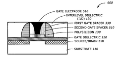
- FIG. 6 is a diagram illustrating formation of a gate electrode 610 according to one embodiment of the invention.
- a gate electrode material such as doped polysilicon or metal is deposited is deposited and polished down to the ILD layer 120 to form a gate electrode 610 .
- the gate electrode 610 have two arc-shaped electrode sidewalls fitting the arc-shaped gate sidewalls of the gate spacers 510 .
- the arc-shaped electrode sidewall decreases in width as function of decreasing height above the polysilicon layer 130 .
- FIG. 7 is a diagram illustrating lines of force 710 according to one embodiment of the invention.
- the lines of force 710 have a number of lines which are approximately equal in length. Since the lines of force 710 are fairly long as decreasing height above the polysilicon layer 130 , the resulting fringing capacitance is reduced.
- FIG. 8 is a flowchart illustrating a process 800 to form a device with reduced fringing capacitance according to one embodiment of the invention.
- the process 800 deposits a gate dielectric layer on the substrate (Block 810 ). Then, the process 800 deposits a doped polysilicon layer on the gate dielectric layer (Block 815 ) using standard techniques. Next, the process 800 deposits a hardmask on the doped polysilicon layer (Block 820 ) to result in a structure as shown in FIG. 1 .
- the process 800 etches the hardmask and the doped polysilicon layer to form a gate stack (Block 825 ) as shown in FIG. 2 .
- the process 800 forms first gate spacers on two sides of the gate stack (Block 830 ) and them forms a silicide structure at the source and drain areas between the substrate and the gate dielectric layer (Block 835 ).
- the process 800 deposits an interlevel dielectric (ILD) layer (Block 840 ) as shown in FIG. 3 .
- ILD interlevel dielectric
- the process 800 etches the hardmask to the doped polysilicon layer to form an opening above the doped polysilicon layer (Block 845 ) as shown in FIG. 4 .
- the process 800 forms two second gate spacers on the doped polysilicon layer in the opening (Block 850 ).
- the second gate spacers have arc-shaped gate sidewalls.
- the process 800 deposits and polishes a gate electrode in the opening (Block 855 ).
- the gate electrode have arc-shaped electrode sidewalls fitting the arc-shaped gate sidewalls as shown in FIG. 6 .
- the process 800 is then terminated.
Abstract
Description
Claims (5)
Priority Applications (2)
| Application Number | Priority Date | Filing Date | Title |
|---|---|---|---|
| US10/256,978 US6784491B2 (en) | 2002-09-27 | 2002-09-27 | MOS devices with reduced fringing capacitance |
| US10/897,291 US7217644B2 (en) | 2002-09-27 | 2004-07-21 | Method of manufacturing MOS devices with reduced fringing capacitance |
Applications Claiming Priority (1)
| Application Number | Priority Date | Filing Date | Title |
|---|---|---|---|
| US10/256,978 US6784491B2 (en) | 2002-09-27 | 2002-09-27 | MOS devices with reduced fringing capacitance |
Related Child Applications (1)
| Application Number | Title | Priority Date | Filing Date |
|---|---|---|---|
| US10/897,291 Division US7217644B2 (en) | 2002-09-27 | 2004-07-21 | Method of manufacturing MOS devices with reduced fringing capacitance |
Publications (2)
| Publication Number | Publication Date |
|---|---|
| US20040061185A1 US20040061185A1 (en) | 2004-04-01 |
| US6784491B2 true US6784491B2 (en) | 2004-08-31 |
Family
ID=32029405
Family Applications (2)
| Application Number | Title | Priority Date | Filing Date |
|---|---|---|---|
| US10/256,978 Expired - Fee Related US6784491B2 (en) | 2002-09-27 | 2002-09-27 | MOS devices with reduced fringing capacitance |
| US10/897,291 Expired - Fee Related US7217644B2 (en) | 2002-09-27 | 2004-07-21 | Method of manufacturing MOS devices with reduced fringing capacitance |
Family Applications After (1)
| Application Number | Title | Priority Date | Filing Date |
|---|---|---|---|
| US10/897,291 Expired - Fee Related US7217644B2 (en) | 2002-09-27 | 2004-07-21 | Method of manufacturing MOS devices with reduced fringing capacitance |
Country Status (1)
| Country | Link |
|---|---|
| US (2) | US6784491B2 (en) |
Cited By (4)
| Publication number | Priority date | Publication date | Assignee | Title |
|---|---|---|---|---|
| US20050023567A1 (en) * | 2003-07-31 | 2005-02-03 | Kazumi Nishinohara | Semiconductor device and method for manufacturing the same |
| US20050214987A1 (en) * | 2004-03-24 | 2005-09-29 | Uday Shah | Replacement gate process for making a semiconductor device that includes a metal gate electrode |
| US20090206406A1 (en) * | 2008-02-15 | 2009-08-20 | Willy Rachmady | Multi-gate device having a t-shaped gate structure |
| US8575683B1 (en) * | 2012-05-16 | 2013-11-05 | United Microelectronics Corp. | Semiconductor device and method of fabricating the same |
Families Citing this family (4)
| Publication number | Priority date | Publication date | Assignee | Title |
|---|---|---|---|---|
| US6185203B1 (en) * | 1997-02-18 | 2001-02-06 | Vixel Corporation | Fibre channel switching fabric |
| US7217977B2 (en) * | 2004-04-19 | 2007-05-15 | Hrl Laboratories, Llc | Covert transformation of transistor properties as a circuit protection method |
| JP4548521B2 (en) * | 2008-07-09 | 2010-09-22 | ソニー株式会社 | Semiconductor device manufacturing method and semiconductor device |
| JP2012099517A (en) | 2010-10-29 | 2012-05-24 | Sony Corp | Semiconductor device and method of manufacturing the same |
Citations (5)
| Publication number | Priority date | Publication date | Assignee | Title |
|---|---|---|---|---|
| US5834816A (en) * | 1991-10-10 | 1998-11-10 | Goldstar Electron Co., Ltd. | MOSFET having tapered gate electrode |
| US6025235A (en) * | 1997-07-09 | 2000-02-15 | Advanced Micro Devices, Inc. | Short channel transistor having resistive gate extensions |
| US6169315B1 (en) * | 1995-12-28 | 2001-01-02 | Hyundai Electronics Industries Co., Ltd. | Metal oxide semiconductor field effect transistor (MOSFET) and method for making thereof |
| US6307226B1 (en) * | 1996-08-22 | 2001-10-23 | Micron Technology, Inc. | Contact openings to electronic components having recessed sidewall structures |
| US6316811B1 (en) * | 1998-06-11 | 2001-11-13 | Chartered Semiconductor Manufacturing Ltd. | Selective CVD TiSi2 deposition with TiSi2 liner |
Family Cites Families (6)
| Publication number | Priority date | Publication date | Assignee | Title |
|---|---|---|---|---|
| US4272880A (en) * | 1979-04-20 | 1981-06-16 | Intel Corporation | MOS/SOS Process |
| US6034401A (en) * | 1998-02-06 | 2000-03-07 | Lsi Logic Corporation | Local interconnection process for preventing dopant cross diffusion in shared gate electrodes |
| US6392271B1 (en) * | 1999-06-28 | 2002-05-21 | Intel Corporation | Structure and process flow for fabrication of dual gate floating body integrated MOS transistors |
| US6326272B1 (en) * | 1999-11-18 | 2001-12-04 | Chartered Semiconductor Manufacturing Ltd. | Method for forming self-aligned elevated transistor |
| US6316323B1 (en) * | 2000-03-21 | 2001-11-13 | United Microelectronics Corp. | Method for forming bridge free silicide by reverse spacer |
| WO2002019396A1 (en) * | 2000-08-29 | 2002-03-07 | Boise State University | Damascene double gated transistors and related manufacturing methods |
-
2002
- 2002-09-27 US US10/256,978 patent/US6784491B2/en not_active Expired - Fee Related
-
2004
- 2004-07-21 US US10/897,291 patent/US7217644B2/en not_active Expired - Fee Related
Patent Citations (5)
| Publication number | Priority date | Publication date | Assignee | Title |
|---|---|---|---|---|
| US5834816A (en) * | 1991-10-10 | 1998-11-10 | Goldstar Electron Co., Ltd. | MOSFET having tapered gate electrode |
| US6169315B1 (en) * | 1995-12-28 | 2001-01-02 | Hyundai Electronics Industries Co., Ltd. | Metal oxide semiconductor field effect transistor (MOSFET) and method for making thereof |
| US6307226B1 (en) * | 1996-08-22 | 2001-10-23 | Micron Technology, Inc. | Contact openings to electronic components having recessed sidewall structures |
| US6025235A (en) * | 1997-07-09 | 2000-02-15 | Advanced Micro Devices, Inc. | Short channel transistor having resistive gate extensions |
| US6316811B1 (en) * | 1998-06-11 | 2001-11-13 | Chartered Semiconductor Manufacturing Ltd. | Selective CVD TiSi2 deposition with TiSi2 liner |
Non-Patent Citations (1)
| Title |
|---|
| Prof. A. Mason, Overview of Semiconductor Fabrication Technology, article, 5 pages. |
Cited By (7)
| Publication number | Priority date | Publication date | Assignee | Title |
|---|---|---|---|---|
| US20050023567A1 (en) * | 2003-07-31 | 2005-02-03 | Kazumi Nishinohara | Semiconductor device and method for manufacturing the same |
| US6911705B2 (en) * | 2003-07-31 | 2005-06-28 | Kabushiki Kaisha Toshiba | MISFET which constitutes a semiconductor integrated circuit improved in integration |
| US20050214987A1 (en) * | 2004-03-24 | 2005-09-29 | Uday Shah | Replacement gate process for making a semiconductor device that includes a metal gate electrode |
| US7208361B2 (en) * | 2004-03-24 | 2007-04-24 | Intel Corporation | Replacement gate process for making a semiconductor device that includes a metal gate electrode |
| US20090206406A1 (en) * | 2008-02-15 | 2009-08-20 | Willy Rachmady | Multi-gate device having a t-shaped gate structure |
| US8264048B2 (en) * | 2008-02-15 | 2012-09-11 | Intel Corporation | Multi-gate device having a T-shaped gate structure |
| US8575683B1 (en) * | 2012-05-16 | 2013-11-05 | United Microelectronics Corp. | Semiconductor device and method of fabricating the same |
Also Published As
| Publication number | Publication date |
|---|---|
| US7217644B2 (en) | 2007-05-15 |
| US20040061185A1 (en) | 2004-04-01 |
| US20040256673A1 (en) | 2004-12-23 |
Similar Documents
| Publication | Publication Date | Title |
|---|---|---|
| US6764884B1 (en) | Method for forming a gate in a FinFET device and thinning a fin in a channel region of the FinFET device | |
| KR100817949B1 (en) | Nonplanar device with stress incorporation layer and method of fabrication | |
| US7256455B2 (en) | Double gate semiconductor device having a metal gate | |
| US10985161B2 (en) | Single diffusion break isolation for gate-all-around field-effect transistor devices | |
| US6787439B2 (en) | Method using planarizing gate material to improve gate critical dimension in semiconductor devices | |
| US7141476B2 (en) | Method of forming a transistor with a bottom gate | |
| US7659561B2 (en) | Methods of fabricating semiconductor devices and structures thereof | |
| CN104810368B (en) | Cmos transistor and forming method thereof | |
| US11588051B2 (en) | Semiconductor device and fabrication method thereof | |
| WO2014005359A1 (en) | Semiconductor component and manufacturing method therefor | |
| CN104538305A (en) | Semiconductor device and method for manufacturing the semiconductor device | |
| CN103545364A (en) | Small-size MOSFET(metal-oxide semiconductor field effect transistor) structure of self-alignment hole and manufacturing method | |
| US6815268B1 (en) | Method for forming a gate in a FinFET device | |
| US20030222319A1 (en) | Semiconductor device having a low dielectric constant film and manufacturing method thereof | |
| US6784491B2 (en) | MOS devices with reduced fringing capacitance | |
| US6911697B1 (en) | Semiconductor device having a thin fin and raised source/drain areas | |
| US6967175B1 (en) | Damascene gate semiconductor processing with local thinning of channel region | |
| US8629028B2 (en) | Metal oxide semiconductor field effect transistor (MOSFET) gate termination | |
| US6524938B1 (en) | Method for gate formation with improved spacer profile control | |
| US8349684B2 (en) | Semiconductor device with high K dielectric control terminal spacer structure | |
| US11069680B2 (en) | FinFET-based integrated circuits with reduced parasitic capacitance | |
| US10748814B2 (en) | Fabrication method of semiconductor device by removing sacrificial layer on gate structures | |
| US6995438B1 (en) | Semiconductor device with fully silicided source/drain and damascence metal gate | |
| US6939770B1 (en) | Method of fabricating semiconductor device having triple LDD structure and lower gate resistance formed with a single implant process | |
| US20140239417A1 (en) | Semiconductor Device Having Electrode and Manufacturing Method Thereof |
Legal Events
| Date | Code | Title | Description |
|---|---|---|---|
| AS | Assignment |
Owner name: INTEL CORPORATION, CALIFORNIA Free format text: ASSIGNMENT OF ASSIGNORS INTEREST;ASSIGNORS:DOYLE, BRIAN;KAVALIEROS, JACK;REEL/FRAME:013338/0066 Effective date: 20020915 |
|
| AS | Assignment |
Owner name: INTEL CORPORATION, CALIFORNIA Free format text: ASSIGNMENT OF ASSIGNORS INTEREST;ASSIGNORS:DOYLE, BRIAN;KAVALIEROS, JACK;REEL/FRAME:013541/0409;SIGNING DATES FROM 20020915 TO 20021122 |
|
| FEPP | Fee payment procedure |
Free format text: PAYOR NUMBER ASSIGNED (ORIGINAL EVENT CODE: ASPN); ENTITY STATUS OF PATENT OWNER: LARGE ENTITY |
|
| FPAY | Fee payment |
Year of fee payment: 4 |
|
| REMI | Maintenance fee reminder mailed | ||
| FPAY | Fee payment |
Year of fee payment: 8 |
|
| REMI | Maintenance fee reminder mailed | ||
| LAPS | Lapse for failure to pay maintenance fees | ||
| STCH | Information on status: patent discontinuation |
Free format text: PATENT EXPIRED DUE TO NONPAYMENT OF MAINTENANCE FEES UNDER 37 CFR 1.362 |
|
| FP | Lapsed due to failure to pay maintenance fee |
Effective date: 20160831 |