US6893504B1 - Multi-port chemical dispense - Google Patents
Multi-port chemical dispense Download PDFInfo
- Publication number
- US6893504B1 US6893504B1 US09/470,835 US47083599A US6893504B1 US 6893504 B1 US6893504 B1 US 6893504B1 US 47083599 A US47083599 A US 47083599A US 6893504 B1 US6893504 B1 US 6893504B1
- Authority
- US
- United States
- Prior art keywords
- receiving surface
- fluid
- nozzle
- axis
- receiver
- Prior art date
- Legal status (The legal status is an assumption and is not a legal conclusion. Google has not performed a legal analysis and makes no representation as to the accuracy of the status listed.)
- Expired - Fee Related, expires
Links
Images


Classifications
-
- H—ELECTRICITY
- H01—ELECTRIC ELEMENTS
- H01L—SEMICONDUCTOR DEVICES NOT COVERED BY CLASS H10
- H01L21/00—Processes or apparatus adapted for the manufacture or treatment of semiconductor or solid state devices or of parts thereof
- H01L21/67—Apparatus specially adapted for handling semiconductor or electric solid state devices during manufacture or treatment thereof; Apparatus specially adapted for handling wafers during manufacture or treatment of semiconductor or electric solid state devices or components ; Apparatus not specifically provided for elsewhere
- H01L21/67005—Apparatus not specifically provided for elsewhere
- H01L21/67011—Apparatus for manufacture or treatment
- H01L21/6715—Apparatus for applying a liquid, a resin, an ink or the like
Definitions
- Silicon wafers are chemically etched to form semiconductor circuits.
- a chemical typically referred to as photoresist is uniformly applied to the surface of the silicon wafer.
- a mask is then interposed between the silicon wafer and an energy source such as a light projector. The energy source is applied through the mask and exposes the photoresist.
- the photoresist is then dissolved with developers, leaving a pattern which is used to etch an image upon the silicon wafer.
- photoresist is applied to the silicon wafer through a nozzle located at the center of the wafer.
- the wafer is rotated and centrifugal force distributes the photoresist along the surface of the wafer.
- Photoresist is expensive and it is therefore desirable to avoid applying more photoresist to a wafer surface than is required to properly coat the surface.
- the present invention may improve the efficiency of coating a silicon wafer with a fluid.
- the fluid is applied at the center of the silicon wafer and at a point between the center of the silicon wafer and the silicon wafer's edge.
- the progress of the fluid across the rotating wafer is monitored. The flow of the fluid is controlled such that excess fluid is not applied to the wafer.
- a first fluid application nozzle is located at the center of the silicon wafer.
- a second fluid application nozzle is interposed between the first application nozzle and the edge of the silicon wafer. A fluid is applied at the first nozzle and the wafer is rotated.
- a sensor monitors the fluid progress and when the fluid reaches a predetermined point or radius, the flow of the fluid from the first nozzle is changed and the fluid is then dispensed through the second nozzle.
- Another embodiment involves a method of applying fluid to a silicon wafer surface.
- a receiving surface is rotated about an axis.
- the receiving surface has an edge remote from the axis.
- a fluid is dispensed from a first nozzle onto the receiving surface at the axis from a first nozzle.
- Fluid is also dispensed onto the receiving surface from a second nozzle interposed between the first nozzle and the edge of the receiving surface.
- Another embodiment involves an apparatus for uniformly coating a silicon wafer surface.
- a receiving surface is rotated about an axis.
- a first nozzle is positioned over the receiving surface proximate the axis.
- a second nozzle is over the receiving surface remote from the first nozzle.
- a method for applying a fluid to a silicon wafer surface by rotating a receiving surface about an axis and dispensing a fluid onto a receiving surface proximate the axis.
- An energy stream is projected against the receiving surface.
- the energy reflected from the receiving surface is monitored to gather information about the receiving surface.
- the gathered information is used to then control the flow of the fluid to the receiving surface.
- a receiving surface is rotatable about an axis.
- a nozzle is positioned over the receiving surface near the axis.
- An emitter projects an energy stream against the receiving surface.
- a receiver monitors the portion of the energy stream reflected from the receiving surface.
- a controller is in communication with the receiver.
- a conduit is in a fluid communication with the nozzle.
- a meter is disposed in the conduit. The meter is in communication with the controller and the meter is adapted to control the flow of the fluid through the conduit to the nozzle.
- Another embodiment involves a method for applying fluid to a silicon wafer.
- a receiving surface is rotated about an axis.
- a fluid is dispensed from a first nozzle over the receiving surface proximate the axis onto the receiving surface.
- the outward flow of the fluid along the receiving surface is monitored and a fluid is dispensed from a second nozzle onto the receiving surface when the outward fluid flow reaches a predetermined radius from the axis.
- an apparatus for applying a fluid to a silicon wafer includes a receiving surface rotatable about an axis.
- the receiving surface has an exterior edge.
- a first conduit has a discharge orifice over the receiving surface near the receiving surface axis.
- the second conduit has a discharge orifice over the receiving surface between the axis and the exterior edge of the receiving surface.
- a first meter is adapted to control the flow of a fluid through the first conduit.
- a second meter is adapted to control the flow of the fluid through the second conduit.
- a monitor is adapted to detect the outward flow of the fluid along the receiving surface.
- a controller is in communication with the monitor and the meters and is adapted to control the meters.
- a receiving surface is rotated about an axis and a fluid is dispensed onto the receiving surface at a first radius from the axis.
- the outward flow of the fluid is monitored and the fluid is dispensed from a second radius from the axis when the fluid dispensed at the first radius flows to a predetermined radius.
- a method for coating a silicon wafer surface involves rotating a receiving surface about an axis. A fluid is dispensed onto the receiving surface at a first radius from the axis. The fluid is sensed at a second radius from the first axis. The flow of the fluid onto the receiving surface at the first radius from the axis is altered and the fluid is dispensed onto the receiving surface near the second radius.
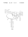
- FIG. 1 is a perspective view of an embodiment of the present invention.
- FIG. 2 is a perspective view of another embodiment of the present invention.
- FIG. 3 is a schematic representation of an aspect of one embodiment of the present invention.
- FIG. 4 is a schematic representation of an alternate embodiment of FIG. 3 .
- a silicon wafer 12 is mounted on a spindle 14 .
- the spindle 14 is rotatable.
- a first nozzle 16 is adjacent the center of the silicon wafer 12 .
- a second nozzle 18 is interposed between the first nozzle 16 and the edge 20 of the silicon wafer 12 .
- a third nozzle 22 is interposed between the second nozzle 18 and the edge 20 of the silicon wafer 12 .
- Flow of a fluid, such as photoresist, through the first, second, and third nozzles is independently controlled.
- the fluid is first applied through the first nozzle 16 .
- the silicon wafer 12 is rotated and centrifugal forces spread the fluid outwardly along the receiving surface of the wafer 12 .
- the fluid flow from the first nozzle 16 may be stopped or decreased and the fluid may then be dispensed from the second nozzle 18 .
- the fluid flow from the second nozzle 18 may be stopped or decreased and the fluid may then be dispensed from the third nozzle 22 .
- the flow of fluid to the first, second, and third nozzles 16 , 18 , 22 may be stopped or ramped down as the subsequent nozzle flow begins or is ramped up so that the flow of fluid to the wafer 12 remains constant. This process provides an even and efficient distribution of a fluid, such as photoresist, across the surface of the silicon wafer 12 .
- the first, second, and third nozzles 16 , 18 , 22 may be approximately two inches apart in one illustrative embodiment.
- photoresist may be applied to the silicon wafer 12 from the first nozzle 16 for 0.5 seconds.
- 0.3 cc of photoresist may be dispensed from the second nozzle 18 for 0.5 seconds.
- 0.3 cc of photoresist may then be flowed from the third nozzle 22 for 0.5 seconds.
- 1.1 cc. of photoresist is applied in 1.5 seconds.
- a fluid is applied to the center of the silicon wafer through a first nozzle 16 .
- the silicon wafer 12 is rotated on a spindle 14 .
- a first energy source 24 such as an infrared or visible light emitter, projects energy to a first observation point 26 on the surface of the silicon wafer 12 .
- a first receiver 28 monitors energy reflected from the first observation point 26 .
- a second energy source 30 projects energy against the surface of the silicon wafer at a second observation point 32 .
- a second receiver monitors 34 the energy reflected from the second observation point 32 .
- the flow of fluid through the first nozzle 16 may be reduced or stopped. Fluid may then be dispensed from the second nozzle 18 until the fluid is detected at the second observation point 32 .
- the flow from the second nozzle 18 may be stopped or reduced and fluid may then be dispensed from the third nozzle 22 for a predetermined period.
- the first and second observation points 26 , 32 may be at the same radius as the second and third nozzles 18 , 22 . Alternatively, it may be advantageous to position the observation points 26 , 32 inward from the second and third nozzles 18 , 22 .
- fluid may be dispensed from the first nozzle 16 by activating the first pump 36 .
- a processor 38 receives information from the first receiver 28 indicating the fluid has spread to the first observation point 26 .
- the processor 38 can then deactivate the first pump 36 and activate the second pump 40 which dispenses photoresist through the second nozzle 18 .
- the processor 38 may deactivate the second pump 40 and activate the third pump 42 for a predetermined period.
- fluid may be dispensed from the first nozzle 16 by activating the pump 44 and valve 46 .
- a processor 38 receives information from the first receiver 28 indicating the fluid has spread to the first observation point 26 .
- the processor 38 can then activate the nozzle 18 by controlling the valve 46 .
- the processor 38 may activate the valve 42 to disperse liquid from the nozzle 22 for a predetermined period.
Abstract
Description
Claims (12)
Priority Applications (1)
| Application Number | Priority Date | Filing Date | Title |
|---|---|---|---|
| US09/470,835 US6893504B1 (en) | 1998-06-05 | 1999-12-23 | Multi-port chemical dispense |
Applications Claiming Priority (2)
| Application Number | Priority Date | Filing Date | Title |
|---|---|---|---|
| US09/092,543 US6642155B1 (en) | 1998-06-05 | 1998-06-05 | Method for applying a fluid to a rotating silicon wafer surface |
| US09/470,835 US6893504B1 (en) | 1998-06-05 | 1999-12-23 | Multi-port chemical dispense |
Related Parent Applications (1)
| Application Number | Title | Priority Date | Filing Date |
|---|---|---|---|
| US09/092,543 Division US6642155B1 (en) | 1998-06-05 | 1998-06-05 | Method for applying a fluid to a rotating silicon wafer surface |
Publications (1)
| Publication Number | Publication Date |
|---|---|
| US6893504B1 true US6893504B1 (en) | 2005-05-17 |
Family
ID=29268632
Family Applications (2)
| Application Number | Title | Priority Date | Filing Date |
|---|---|---|---|
| US09/092,543 Expired - Lifetime US6642155B1 (en) | 1998-06-05 | 1998-06-05 | Method for applying a fluid to a rotating silicon wafer surface |
| US09/470,835 Expired - Fee Related US6893504B1 (en) | 1998-06-05 | 1999-12-23 | Multi-port chemical dispense |
Family Applications Before (1)
| Application Number | Title | Priority Date | Filing Date |
|---|---|---|---|
| US09/092,543 Expired - Lifetime US6642155B1 (en) | 1998-06-05 | 1998-06-05 | Method for applying a fluid to a rotating silicon wafer surface |
Country Status (1)
| Country | Link |
|---|---|
| US (2) | US6642155B1 (en) |
Families Citing this family (7)
| Publication number | Priority date | Publication date | Assignee | Title |
|---|---|---|---|---|
| WO2005028705A1 (en) * | 2003-09-19 | 2005-03-31 | Applied Materials, Inc. | Apparatus and method of detecting the electroless deposition endpoint |
| KR100636035B1 (en) * | 2003-11-08 | 2006-10-18 | 삼성전자주식회사 | Method and apparatus for drying a wafer and wafer treatment apparatus comprising the wafer drying apparatus |
| US20050148203A1 (en) * | 2003-12-29 | 2005-07-07 | Shirley Paul D. | Method, apparatus, system and computer-readable medium for in situ photoresist thickness characterization |
| US20050172894A1 (en) * | 2004-02-10 | 2005-08-11 | Farnworth Warren M. | Selective deposition system and method for initiating deposition at a defined starting surface |
| US7670643B2 (en) * | 2004-07-01 | 2010-03-02 | Tokyo Electron Limited | Method and system for dispensing resist solution |
| US11624607B2 (en) | 2020-01-06 | 2023-04-11 | Tokyo Electron Limited | Hardware improvements and methods for the analysis of a spinning reflective substrates |
| US11738363B2 (en) | 2021-06-07 | 2023-08-29 | Tokyo Electron Limited | Bath systems and methods thereof |
Citations (3)
| Publication number | Priority date | Publication date | Assignee | Title |
|---|---|---|---|---|
| US5393624A (en) * | 1988-07-29 | 1995-02-28 | Tokyo Electron Limited | Method and apparatus for manufacturing a semiconductor device |
| US5646071A (en) * | 1995-01-19 | 1997-07-08 | Taiwan Semiconductor Manufacturing Company, Ltd. | Equipment and method for applying a liquid layer |
| US5772764A (en) * | 1995-10-13 | 1998-06-30 | Tokyo Electron Limited | Coating apparatus |
Family Cites Families (9)
| Publication number | Priority date | Publication date | Assignee | Title |
|---|---|---|---|---|
| JPS63136528A (en) * | 1986-11-27 | 1988-06-08 | Mitsubishi Electric Corp | Applicator for treatment liquid |
| US5238866A (en) * | 1991-09-11 | 1993-08-24 | GmbH & Co. Ingenieurburo Berlin Biotronik Mess- und Therapiegerate | Plasma enhanced chemical vapor deposition process for producing an amorphous semiconductive surface coating |
| US5298966A (en) * | 1992-11-10 | 1994-03-29 | Advanced Micro Devices, Inc. | Measurement system |
| SG130022A1 (en) * | 1993-03-25 | 2007-03-20 | Tokyo Electron Ltd | Method of forming coating film and apparatus therefor |
| US5665640A (en) * | 1994-06-03 | 1997-09-09 | Sony Corporation | Method for producing titanium-containing thin films by low temperature plasma-enhanced chemical vapor deposition using a rotating susceptor reactor |
| JP2825077B2 (en) * | 1996-01-26 | 1998-11-18 | 日本電気株式会社 | Semiconductor device manufacturing method and manufacturing apparatus |
| JP3516195B2 (en) * | 1996-05-28 | 2004-04-05 | 東京エレクトロン株式会社 | Method and apparatus for forming coating film |
| JP3245812B2 (en) * | 1996-08-30 | 2002-01-15 | 東京エレクトロン株式会社 | Liquid treatment method and apparatus |
| TW389949B (en) * | 1997-01-30 | 2000-05-11 | Tokyo Electron Ltd | Method and apparatus for coating and development of the photo-resist solution |
-
1998
- 1998-06-05 US US09/092,543 patent/US6642155B1/en not_active Expired - Lifetime
-
1999
- 1999-12-23 US US09/470,835 patent/US6893504B1/en not_active Expired - Fee Related
Patent Citations (3)
| Publication number | Priority date | Publication date | Assignee | Title |
|---|---|---|---|---|
| US5393624A (en) * | 1988-07-29 | 1995-02-28 | Tokyo Electron Limited | Method and apparatus for manufacturing a semiconductor device |
| US5646071A (en) * | 1995-01-19 | 1997-07-08 | Taiwan Semiconductor Manufacturing Company, Ltd. | Equipment and method for applying a liquid layer |
| US5772764A (en) * | 1995-10-13 | 1998-06-30 | Tokyo Electron Limited | Coating apparatus |
Also Published As
| Publication number | Publication date |
|---|---|
| US6642155B1 (en) | 2003-11-04 |
Similar Documents
| Publication | Publication Date | Title |
|---|---|---|
| EP0110558B1 (en) | Method and apparatus for use in developing resist film | |
| US5952050A (en) | Chemical dispensing system for semiconductor wafer processing | |
| US4688918A (en) | Negative type photoresist developing apparatus | |
| US4640846A (en) | Semiconductor spin coating method | |
| EP0643334A1 (en) | Resist deposition | |
| US5646071A (en) | Equipment and method for applying a liquid layer | |
| US6893504B1 (en) | Multi-port chemical dispense | |
| JPH08330258A (en) | Rinse spray bar that is used for chemical machinery grind | |
| US7942967B2 (en) | Method and system of coating polymer solution on a substrate in a solvent saturated chamber | |
| US6024249A (en) | Fluid delivery system using an optical sensor to monitor for gas bubbles | |
| KR20010089163A (en) | Improved yield and line width performance for liquid polymers and other materials | |
| JPH08139007A (en) | Cleaning method and apparatus | |
| JP3164108B2 (en) | Method and apparatus for coating a substrate surface to a uniform thickness | |
| US6592939B1 (en) | System for and method of using developer as a solvent to spread photoresist faster and reduce photoresist consumption | |
| JP3393534B2 (en) | Processing liquid supply nozzle system | |
| KR100672928B1 (en) | Photoresist coating equipment | |
| JPH044850Y2 (en) | ||
| US6403500B1 (en) | Cross-shaped resist dispensing system and method | |
| JPS581144A (en) | Method for coating photoresist | |
| JP2004134448A (en) | Developing device for manufacturing semiconductor | |
| US5908041A (en) | Method for cleaning a photoresist developer spray stream nozzle | |
| US20070000516A1 (en) | Device and method for cleaning the edges of substrates | |
| KR20220011893A (en) | Apparatus for treating substrate | |
| JP2558490B2 (en) | Development device | |
| JPH07161683A (en) | Wet etching end point detecting method and wet etching device |
Legal Events
| Date | Code | Title | Description |
|---|---|---|---|
| FPAY | Fee payment |
Year of fee payment: 4 |
|
| FPAY | Fee payment |
Year of fee payment: 8 |
|
| AS | Assignment |
Owner name: U.S. BANK NATIONAL ASSOCIATION, AS COLLATERAL AGENT, CALIFORNIA Free format text: SECURITY INTEREST;ASSIGNOR:MICRON TECHNOLOGY, INC.;REEL/FRAME:038669/0001 Effective date: 20160426 Owner name: U.S. BANK NATIONAL ASSOCIATION, AS COLLATERAL AGEN Free format text: SECURITY INTEREST;ASSIGNOR:MICRON TECHNOLOGY, INC.;REEL/FRAME:038669/0001 Effective date: 20160426 |
|
| AS | Assignment |
Owner name: MORGAN STANLEY SENIOR FUNDING, INC., AS COLLATERAL AGENT, MARYLAND Free format text: PATENT SECURITY AGREEMENT;ASSIGNOR:MICRON TECHNOLOGY, INC.;REEL/FRAME:038954/0001 Effective date: 20160426 Owner name: MORGAN STANLEY SENIOR FUNDING, INC., AS COLLATERAL Free format text: PATENT SECURITY AGREEMENT;ASSIGNOR:MICRON TECHNOLOGY, INC.;REEL/FRAME:038954/0001 Effective date: 20160426 |
|
| REMI | Maintenance fee reminder mailed | ||
| LAPS | Lapse for failure to pay maintenance fees | ||
| AS | Assignment |
Owner name: U.S. BANK NATIONAL ASSOCIATION, AS COLLATERAL AGENT, CALIFORNIA Free format text: CORRECTIVE ASSIGNMENT TO CORRECT THE REPLACE ERRONEOUSLY FILED PATENT #7358718 WITH THE CORRECT PATENT #7358178 PREVIOUSLY RECORDED ON REEL 038669 FRAME 0001. ASSIGNOR(S) HEREBY CONFIRMS THE SECURITY INTEREST;ASSIGNOR:MICRON TECHNOLOGY, INC.;REEL/FRAME:043079/0001 Effective date: 20160426 Owner name: U.S. BANK NATIONAL ASSOCIATION, AS COLLATERAL AGEN Free format text: CORRECTIVE ASSIGNMENT TO CORRECT THE REPLACE ERRONEOUSLY FILED PATENT #7358718 WITH THE CORRECT PATENT #7358178 PREVIOUSLY RECORDED ON REEL 038669 FRAME 0001. ASSIGNOR(S) HEREBY CONFIRMS THE SECURITY INTEREST;ASSIGNOR:MICRON TECHNOLOGY, INC.;REEL/FRAME:043079/0001 Effective date: 20160426 |
|
| STCH | Information on status: patent discontinuation |
Free format text: PATENT EXPIRED DUE TO NONPAYMENT OF MAINTENANCE FEES UNDER 37 CFR 1.362 |
|
| FP | Lapsed due to failure to pay maintenance fee |
Effective date: 20170517 |
|
| AS | Assignment |
Owner name: MICRON TECHNOLOGY, INC., IDAHO Free format text: RELEASE BY SECURED PARTY;ASSIGNOR:U.S. BANK NATIONAL ASSOCIATION, AS COLLATERAL AGENT;REEL/FRAME:047243/0001 Effective date: 20180629 |
|
| AS | Assignment |
Owner name: MICRON TECHNOLOGY, INC., IDAHO Free format text: RELEASE BY SECURED PARTY;ASSIGNOR:MORGAN STANLEY SENIOR FUNDING, INC., AS COLLATERAL AGENT;REEL/FRAME:050937/0001 Effective date: 20190731 |