US6971793B2 - Test handler temperature monitoring system - Google Patents
Test handler temperature monitoring system Download PDFInfo
- Publication number
- US6971793B2 US6971793B2 US10/395,401 US39540103A US6971793B2 US 6971793 B2 US6971793 B2 US 6971793B2 US 39540103 A US39540103 A US 39540103A US 6971793 B2 US6971793 B2 US 6971793B2
- Authority
- US
- United States
- Prior art keywords
- temperature
- heat transfer
- test
- radiation sensor
- electronic device
- Prior art date
- Legal status (The legal status is an assumption and is not a legal conclusion. Google has not performed a legal analysis and makes no representation as to the accuracy of the status listed.)
- Expired - Lifetime
Links
- 238000012360 testing method Methods 0.000 title claims abstract description 152
- 238000012544 monitoring process Methods 0.000 title abstract description 6
- 230000005855 radiation Effects 0.000 claims abstract description 64
- 238000012546 transfer Methods 0.000 claims description 35
- 238000000034 method Methods 0.000 claims description 22
- 239000000969 carrier Substances 0.000 claims description 15
- 230000008859 change Effects 0.000 claims description 3
- 239000000463 material Substances 0.000 claims description 3
- 239000002826 coolant Substances 0.000 claims 15
- 230000001276 controlling effect Effects 0.000 claims 4
- 238000012423 maintenance Methods 0.000 claims 4
- 238000004891 communication Methods 0.000 claims 3
- 230000000694 effects Effects 0.000 claims 2
- 238000011084 recovery Methods 0.000 claims 2
- 230000005540 biological transmission Effects 0.000 claims 1
- 230000001105 regulatory effect Effects 0.000 claims 1
- 238000002360 preparation method Methods 0.000 abstract description 3
- 239000004065 semiconductor Substances 0.000 abstract description 3
- 238000010438 heat treatment Methods 0.000 description 20
- 238000001816 cooling Methods 0.000 description 13
- 238000009413 insulation Methods 0.000 description 6
- 230000008646 thermal stress Effects 0.000 description 5
- 230000008569 process Effects 0.000 description 4
- 210000002445 nipple Anatomy 0.000 description 3
- IJGRMHOSHXDMSA-UHFFFAOYSA-N Atomic nitrogen Chemical compound N#N IJGRMHOSHXDMSA-UHFFFAOYSA-N 0.000 description 2
- 238000007792 addition Methods 0.000 description 2
- 238000007405 data analysis Methods 0.000 description 2
- 238000004519 manufacturing process Methods 0.000 description 2
- 238000005259 measurement Methods 0.000 description 2
- 238000012986 modification Methods 0.000 description 2
- 230000004048 modification Effects 0.000 description 2
- 238000010137 moulding (plastic) Methods 0.000 description 2
- 230000004044 response Effects 0.000 description 2
- 230000008901 benefit Effects 0.000 description 1
- 238000009529 body temperature measurement Methods 0.000 description 1
- 230000001143 conditioned effect Effects 0.000 description 1
- 230000003750 conditioning effect Effects 0.000 description 1
- 238000013461 design Methods 0.000 description 1
- 238000001514 detection method Methods 0.000 description 1
- 238000009826 distribution Methods 0.000 description 1
- 238000003780 insertion Methods 0.000 description 1
- 230000037431 insertion Effects 0.000 description 1
- 239000007788 liquid Substances 0.000 description 1
- 239000012528 membrane Substances 0.000 description 1
- 239000002184 metal Substances 0.000 description 1
- 229910052757 nitrogen Inorganic materials 0.000 description 1
- 238000004806 packaging method and process Methods 0.000 description 1
- 230000000704 physical effect Effects 0.000 description 1
- 238000012545 processing Methods 0.000 description 1
- 230000035939 shock Effects 0.000 description 1
- 238000007619 statistical method Methods 0.000 description 1
- 239000000758 substrate Substances 0.000 description 1
Images


Classifications
-
- G—PHYSICS
- G01—MEASURING; TESTING
- G01R—MEASURING ELECTRIC VARIABLES; MEASURING MAGNETIC VARIABLES
- G01R31/00—Arrangements for testing electric properties; Arrangements for locating electric faults; Arrangements for electrical testing characterised by what is being tested not provided for elsewhere
- G01R31/28—Testing of electronic circuits, e.g. by signal tracer
- G01R31/2851—Testing of integrated circuits [IC]
- G01R31/2855—Environmental, reliability or burn-in testing
- G01R31/2872—Environmental, reliability or burn-in testing related to electrical or environmental aspects, e.g. temperature, humidity, vibration, nuclear radiation
- G01R31/2874—Environmental, reliability or burn-in testing related to electrical or environmental aspects, e.g. temperature, humidity, vibration, nuclear radiation related to temperature
-
- G—PHYSICS
- G01—MEASURING; TESTING
- G01J—MEASUREMENT OF INTENSITY, VELOCITY, SPECTRAL CONTENT, POLARISATION, PHASE OR PULSE CHARACTERISTICS OF INFRARED, VISIBLE OR ULTRAVIOLET LIGHT; COLORIMETRY; RADIATION PYROMETRY
- G01J5/00—Radiation pyrometry, e.g. infrared or optical thermometry
-
- G—PHYSICS
- G01—MEASURING; TESTING
- G01J—MEASUREMENT OF INTENSITY, VELOCITY, SPECTRAL CONTENT, POLARISATION, PHASE OR PULSE CHARACTERISTICS OF INFRARED, VISIBLE OR ULTRAVIOLET LIGHT; COLORIMETRY; RADIATION PYROMETRY
- G01J5/00—Radiation pyrometry, e.g. infrared or optical thermometry
- G01J5/0096—Radiation pyrometry, e.g. infrared or optical thermometry for measuring wires, electrical contacts or electronic systems
-
- G—PHYSICS
- G01—MEASURING; TESTING
- G01J—MEASUREMENT OF INTENSITY, VELOCITY, SPECTRAL CONTENT, POLARISATION, PHASE OR PULSE CHARACTERISTICS OF INFRARED, VISIBLE OR ULTRAVIOLET LIGHT; COLORIMETRY; RADIATION PYROMETRY
- G01J5/00—Radiation pyrometry, e.g. infrared or optical thermometry
- G01J5/10—Radiation pyrometry, e.g. infrared or optical thermometry using electric radiation detectors
- G01J5/12—Radiation pyrometry, e.g. infrared or optical thermometry using electric radiation detectors using thermoelectric elements, e.g. thermocouples
-
- G—PHYSICS
- G01—MEASURING; TESTING
- G01R—MEASURING ELECTRIC VARIABLES; MEASURING MAGNETIC VARIABLES
- G01R1/00—Details of instruments or arrangements of the types included in groups G01R5/00 - G01R13/00 and G01R31/00
- G01R1/02—General constructional details
- G01R1/04—Housings; Supporting members; Arrangements of terminals
- G01R1/0408—Test fixtures or contact fields; Connectors or connecting adaptors; Test clips; Test sockets
- G01R1/0433—Sockets for IC's or transistors
- G01R1/0441—Details
- G01R1/0458—Details related to environmental aspects, e.g. temperature
-
- G—PHYSICS
- G01—MEASURING; TESTING
- G01R—MEASURING ELECTRIC VARIABLES; MEASURING MAGNETIC VARIABLES
- G01R31/00—Arrangements for testing electric properties; Arrangements for locating electric faults; Arrangements for electrical testing characterised by what is being tested not provided for elsewhere
- G01R31/28—Testing of electronic circuits, e.g. by signal tracer
- G01R31/2851—Testing of integrated circuits [IC]
- G01R31/2855—Environmental, reliability or burn-in testing
- G01R31/286—External aspects, e.g. related to chambers, contacting devices or handlers
- G01R31/2865—Holding devices, e.g. chucks; Handlers or transport devices
- G01R31/2867—Handlers or transport devices, e.g. loaders, carriers, trays
-
- G—PHYSICS
- G01—MEASURING; TESTING
- G01R—MEASURING ELECTRIC VARIABLES; MEASURING MAGNETIC VARIABLES
- G01R31/00—Arrangements for testing electric properties; Arrangements for locating electric faults; Arrangements for electrical testing characterised by what is being tested not provided for elsewhere
- G01R31/28—Testing of electronic circuits, e.g. by signal tracer
- G01R31/302—Contactless testing
- G01R31/3025—Wireless interface with the DUT
Definitions
- the invention relates to a method and apparatus for measuring surface temperature of electronic devices while they are undergoing a test handling process in a semiconductor test handler. More specifically, the apparatus is equipped with temperature sensors to monitor the temperature of the electronic devices as they are prepared for electrical testing.
- the devices are electrically tested after the packages have been molded. Normally, the devices are tested only after they have been brought to a certain predetermined temperature by heating or cooling. This predetermined temperature usually reflects the expected operating environments for the devices being tested. A typical testing temperature is about 90–100° C., but different testing temperatures may be selected depending on the type of device being tested. The following description shall focus on heating the electronic devices before electrical testing, although it should be appreciated that the invention is equally applicable to the cooling of electronic devices before testing.
- test handlers have been developed in the integrated circuit packaging industry to perform final electrical tests on electronic devices automatically at high speeds.
- Test handlers feed electronic devices to and away from a test platform at desired rates of speed.
- These test handlers usually include heating chamber(s) within which the electronic devices to be tested are first soaked to the specified test temperature before they are tested on the test platform.
- Temperature sensors are commonly used for such temperature measurements. Examples are contact-type thermocouples and resistive temperature devices (RTD). However, the ability of test handlers that employ these types of sensors to detect a temperature of a moving test device inside the test handler is limited.
- a temperature sensor embedded in a test device is used to record the true device temperature and to calibrate the sensor readings.
- a temperature reading of the sensor over the heating chamber will vary with different airflows according to chamber geometry. Sensors located at the edges of the chamber encounter lower flow rates whereas sensors located at the center encounter higher flow rates. This means that the sensor readings cannot accurately represent the surface temperature. This becomes significant when a carrier for the test device has a relatively high heat loss or has its own temperature distribution.
- test handler Using non-contact type sensing on a test handler would allow probing without affecting the temperature of the test device, especially when the test device is small. It allows the test handler to handle different types of test devices without any major design change in the system.
- thermopile sensors can complete a measurement within one second. Furthermore, by not locating the temperature sensor inside the thermally conditioned chamber, this subjects lesser thermal stress on the sensor and reduces machine down-time. Thus, a contactless method for sensing a temperature of a test device is desirable. Radiation sensors are especially suitable where the test device contains a plastic molding which provides a consistent and large emissivity.
- the invention seeks to provide a temperature sensor which senses temperature by detecting heat that is radiated from a test device to thereby avoid some of the disadvantages associated with prior art contact-type sensors.
- a temperature monitoring system for a test handler comprising a preparation stage for bringing a test device to a predetermined temperature; a test platform for testing the test device at said predetermined temperature; and at least one radiation sensor adapted for detecting a surface temperature of the test device by measuring radiation emitted from the test device.
- a method for monitoring temperature in a test handler comprising the steps of bringing a test device to a predetermined temperature while providing at least one radiation sensor to detect a surface temperature of the test device by measuring radiation emitted from the test device; and testing the test device at said predetermined temperature.
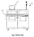
- FIG. 1 is a front view of a typical test handler machine
- FIG. 2 is a schematic illustration of a test handler module according to the preferred embodiment of the invention.
- FIG. 3 is a graphical illustration of a typical heating sequence as a test device is prepared for testing at a test platform
- FIG. 4 is an isometric view of a thermopile sensor according to the preferred embodiment of the invention.
- FIG. 5 is a top view of the thermopile sensor from direction C of FIG. 4 ;
- FIG. 6 is a cross-sectional view of the thermopile sensor along section A—A of FIG. 5 ;
- FIG. 7 is an exploded view of the thermopile sensor of FIG. 4 ;
- FIG. 8 is an isometric view of a preheat location of the test handler module according to the preferred embodiment of the invention.
- FIG. 1 is a front view of a typical test handler machine 10 .
- the test handler machine 10 may include a display screen 11 to view in real time process parameters associated with the test handling process, as well as to facilitate a user to set process parameters such as heating temperatures.
- the test handler machine 10 has a preparation stage, which may be in the form of a preheat location 12 , where test devices are heated prior to testing.
- FIG. 2 is a schematic illustration of a test handler module, including a preheat location 12 and test platform 20 , according to the preferred embodiment of the invention.
- the test handler module has an outer wall and inner case 14 .
- To transport test devices (not shown) around the inner case 14 a number of movable carriers 16 are integrated therein.
- Each carrier 16 preferably carries a test device, which may comprise a leadframe, Ball-Grid Array or other electronic package.
- In the preheat location 12 of the test handler module there is an on-load position 18 where test devices are introduced into the inner case 14 and placed onto the carriers 16 .
- the carriers 16 are then moved along heating chambers, which may be further divided into different temperature or heating zones, wherein heaters are positioned below the carriers 16 .
- the heating chambers are designed such that the temperatures of the test devices are gradually raised to a predetermined temperature to prepare them for testing at the test platform 20 .
- Interspersed within inner case are a number of radiation sensors, such as thermopile sensors 28 , 28 A–D, to measure temperatures of test devices that pass under the sensors.
- the inner case 14 may also include a liquid nitrogen control valve 24 and a cooling fan 26 that are controllable and adjusted as appropriate if say, the targeted device temperature in the system is below ambient temperature and cooling is required.
- thermopile sensors 28 , 28 A–D detect radiation from the test devices, they produce an analog output, which corresponds to the temperature of the test devices sensed by the thermopile sensors 28 , 28 A–D.
- An Analogue-to-Digital converter 30 converts the output of the thermopile sensors 28 , 28 A–D from analogue to digital form.
- the Analogue-to-Digital converter 30 is electrically connected to a computer 32 and the digital output is received by the computer 32 for processing.
- a temperature control unit 34 which receives input from the computer 32 , is in turn electrically connected to and controls a temperature controller, which controls heating/cooling parameters in the test handling module.
- the computer 32 may control factors such as a heating period of the test devices according to the soak time of the test devices desired and selected by a user, through the utilization of test device temperatures sensed by the thermopile sensors 28 , 28 A–D.
- the output from the computer 32 is applied to the temperature controller 34 , which in turn operates the temperature controller according to the output from the computer 32 to make precise automatic temperature control possible.
- Information from the computer 32 may optionally be further processed for statistical analysis 36 .
- Statistical and other data may be displayed in real time 38 by output to the display screen 11 for viewing by a user.
- the parameters that may be displayed on display screen 11 include temperature, standard deviation and trend data.
- FIG. 3 is a graphical illustration of a typical heating sequence as a test device is prepared for testing at a test platform 20 .
- a carrier 16 carrying a test device goes through the on-load position 18 , different heating zones (Zones A–C), the test platform 20 and finally to the off-load position 22 .
- Package temperatures of the test devices are monitored using thermopile sensors 28 , 28 A–D located in different zones of the heating chamber directly over the carriers 16 and devices to be tested. Reading FIG. 3 with FIG.
- thermopile sensor 28 is located adjacent to the on-load position 18 , a second thermopile sensor 28 A is located at Zone A, a third thermopile sensor 28 B is located at Zone B, a fourth thermopile sensor 28 C is located at Zone C, and a fifth thermopile sensor 28 D is located at the test platform 20 .
- Information collected from the thermopile sensors 28 , 28 A–D may be compiled to form the graphical illustration of FIG. 3 , which may be output to the display screen 11 for monitoring by a user.
- FIG. 4 is an isometric view of a thermopile sensor 28 according to the preferred embodiment of the invention.
- the thermopile sensor 28 generally comprises a sensor cover 30 , a sensor fixture 32 , threaded nipples 34 conveying compressed dry air to and away from the sensor 28 and a cooling support 36 .
- FIG. 5 is a top view of the thermopile sensor 28 from direction C of FIG. 4 .
- the threaded nipples 34 carry compressed air into and out of the thermopile sensor 28 .
- the compressed dry air is meant to cool the thermopile sensor 28 to avoid thermal stress or other interference from the heating chambers of the preheating location 12 .
- FIG. 6 is a cross-sectional view of the thermopile sensor 28 along section A—A of FIG. 5 .
- This view shows a thermopile device or integrated circuit (“IC”) 38 positioned within the device.
- the thermopile IC 38 is attached to the sensor fixture 32 and is in contact with the cooling support 36 . Air channels 42 in the cooling support 36 carry cooling compressed air to cool the thermopile sensor 28 . Therefore, the cooling support 38 acts like a heat-sink to draw heat away from the thermopile IC 38 . This helps to ensure that the thermopile sensor 28 is not subjected to temperature changes inside the heating chambers, thereby allowing more precise measurement by preserving the physical properties of the thermopile IC 38 . Moreover, by reducing thermal stress or shock, the life of the thermopile sensor 28 can be extended as compared with traditional sensor devices, which are located inside the heating chambers and are subjected to thermal stresses.
- the thermopile IC 38 includes a substrate having a membrane structure, a first insulation layer and a second insulation layer successively formed thereon. Two thermocouples formed on the second insulation layer are connected in series. Each thermocouple has a hot junction and a cold junction.
- the thermopile IC 38 further includes a temperature sensor formed at one side of the second insulation layer.
- the thermopile IC 38 further includes a third insulation layer and a black body formed on the third insulation layer over the hot junctions.
- radiation intensity is proportional to the fourth power of the temperature of an object, and thus the radiation intensity increases sharply as surface temperature of the object rises.
- This property may be used to calculate surface temperature of an object, as employed in the preferred embodiment.
- a wave-guide 39 is formed in the cooling support 36 .
- the wave-guide 39 preferably has a polished wall to reduce scattering of radiation waves before they reach the thermopile IC 38 .
- test devices in the form of IC package units 40 that are carried underneath the opening of the sensing wave-guide 39 .
- the thermopile sensor 28 provides for precise temperature conditioning or monitoring by sensing an amount of radiation energy emitted from a test device. Since IC packages are generally encapsulated using dark plastic molding, heat radiation properties of the body comprising plastic material can be taken advantage of.
- the thermopile sensor 28 senses the radiation temperature of the test device by utilizing a radiation rate difference between a black body and the dark body of the test device upon heating. Thus, the thermopile sensor generates a voltage corresponding to an infrared ray received through the wave-guide 39 , which channels infrared ray produced by radiation from the test devices to the thermopile IC 38 .
- FIG. 7 is an exploded view of the thermopile sensor of FIG. 4 . It shows, in sequence, the sensor cover 30 , the sensor fixture 32 , the thermopile IC 38 , the threaded nipples 34 and cooling support 36 .
- the cooling support 36 includes a wave-guide 39 dimensioned to allow insertion of the thermopile IC 38 .
- FIG. 8 is an isometric view of a preheat location 12 of the test handler module according to the preferred embodiment of the invention.
- the preheat chambers are enclosed by a housing or an upper casing 50 as the carriers 16 are carried within the cavities of the chambers and are heated.
- Carriers 16 are introduced via an on-load position 18 and then moved into the preheat chambers underneath the upper casing 50 .
- a number of thermopile sensors 28 are mounted on the housing or upper casing 50 over the heat chambers. It would be appreciated that the wave-guide 39 of the thermopile sensors 28 should extend through and be exposed on an underside of the preheat cover facing the test devices 40 of the carriers 16 , so that radiation from the test devices may be received by the thermopile IC 38 . After passing through the preheating zone, the carriers 16 are moved to the test platform (not shown in FIG. 8 ) for testing of the test devices.
- the invention makes it possible to achieve contactless detection of surface temperatures of electronic devices during production. Instead of measuring temperatures of heat transfer media (eg. forced hot/cold air), true surface temperature is monitored inside the preheating and testing locations. Temperature data measured can be used for alarms, feedback control, or data analysis. Real-time temperature that can be displayed on a display screen allows a user to closely monitor the rate of temperature change of test devices. Data analysis can further include the correlation of yield loss and temperature profile or thermal instability.
- temperatures of heat transfer media eg. forced hot/cold air
Abstract
The invention provides a temperature monitoring system for a semiconductor test handler. A preparation stage brings a test device to a predetermined temperature for testing at a test platform at said predetermined temperature. At least one radiation sensor, such as a thermopile device, is employed in the test handler for detecting a surface temperature of the test device by measuring radiation emitted from the test device.
Description
The invention relates to a method and apparatus for measuring surface temperature of electronic devices while they are undergoing a test handling process in a semiconductor test handler. More specifically, the apparatus is equipped with temperature sensors to monitor the temperature of the electronic devices as they are prepared for electrical testing.
During the manufacture of some electronic devices, in particular, integrated circuit packages in the semiconductor industry, it is necessary for the devices to be electrically tested after the packages have been molded. Normally, the devices are tested only after they have been brought to a certain predetermined temperature by heating or cooling. This predetermined temperature usually reflects the expected operating environments for the devices being tested. A typical testing temperature is about 90–100° C., but different testing temperatures may be selected depending on the type of device being tested. The following description shall focus on heating the electronic devices before electrical testing, although it should be appreciated that the invention is equally applicable to the cooling of electronic devices before testing.
Various testing devices have been developed to perform such electrical tests. For example, test handlers have been developed in the integrated circuit packaging industry to perform final electrical tests on electronic devices automatically at high speeds. Test handlers feed electronic devices to and away from a test platform at desired rates of speed. These test handlers usually include heating chamber(s) within which the electronic devices to be tested are first soaked to the specified test temperature before they are tested on the test platform.
When the electronic devices are passing through the heating chambers, their temperatures need to be constantly monitored so that gradual heating of the devices can be attained without subjecting them to excessive thermal stress or damaging them. Temperature sensors are commonly used for such temperature measurements. Examples are contact-type thermocouples and resistive temperature devices (RTD). However, the ability of test handlers that employ these types of sensors to detect a temperature of a moving test device inside the test handler is limited.
Instead of directly measuring the surface temperature of test devices, such temperature sensors measure the temperature of the heat transfer media, usually forced heated air or a metal holder. Prior to this, a temperature sensor embedded in a test device is used to record the true device temperature and to calibrate the sensor readings. Furthermore, when using a single temperature sensor inside a large volume of a thermally controlled chamber, a temperature reading of the sensor over the heating chamber will vary with different airflows according to chamber geometry. Sensors located at the edges of the chamber encounter lower flow rates whereas sensors located at the center encounter higher flow rates. This means that the sensor readings cannot accurately represent the surface temperature. This becomes significant when a carrier for the test device has a relatively high heat loss or has its own temperature distribution.
Using non-contact type sensing on a test handler would allow probing without affecting the temperature of the test device, especially when the test device is small. It allows the test handler to handle different types of test devices without any major design change in the system.
Moreover, soak time is becoming shorter and temperature sensors with faster response times are required. Whilst typical contacting sensors have response times that are more than a few seconds, radiation sensors such as thermopile sensors can complete a measurement within one second. Furthermore, by not locating the temperature sensor inside the thermally conditioned chamber, this subjects lesser thermal stress on the sensor and reduces machine down-time. Thus, a contactless method for sensing a temperature of a test device is desirable. Radiation sensors are especially suitable where the test device contains a plastic molding which provides a consistent and large emissivity.
Therefore, the invention seeks to provide a temperature sensor which senses temperature by detecting heat that is radiated from a test device to thereby avoid some of the disadvantages associated with prior art contact-type sensors.
According to a first aspect of the invention, there is provided a temperature monitoring system for a test handler comprising a preparation stage for bringing a test device to a predetermined temperature; a test platform for testing the test device at said predetermined temperature; and at least one radiation sensor adapted for detecting a surface temperature of the test device by measuring radiation emitted from the test device.
According to a second aspect of the invention, there is provided a method for monitoring temperature in a test handler comprising the steps of bringing a test device to a predetermined temperature while providing at least one radiation sensor to detect a surface temperature of the test device by measuring radiation emitted from the test device; and testing the test device at said predetermined temperature.
It will be convenient to hereinafter describe the invention in greater detail by reference to the accompanying drawings, which illustrate one embodiment of the invention. The particularity of the drawings and the related description is not to be understood as superseding the generality of the broad identification of the invention as defined by the claims.
After preheating in the preheat location 12, the carriers 16 are moved to the test platform 20 for electrical testing. After testing, the carriers 16 are transported towards the off-load location 22 for removal of the test devices from the test handler module. The inner case 14 may also include a liquid nitrogen control valve 24 and a cooling fan 26 that are controllable and adjusted as appropriate if say, the targeted device temperature in the system is below ambient temperature and cooling is required.
As the thermopile sensors 28, 28A–D detect radiation from the test devices, they produce an analog output, which corresponds to the temperature of the test devices sensed by the thermopile sensors 28, 28A–D. An Analogue-to-Digital converter 30 converts the output of the thermopile sensors 28, 28A–D from analogue to digital form. The Analogue-to-Digital converter 30 is electrically connected to a computer 32 and the digital output is received by the computer 32 for processing. A temperature control unit 34, which receives input from the computer 32, is in turn electrically connected to and controls a temperature controller, which controls heating/cooling parameters in the test handling module. Thus, the computer 32 may control factors such as a heating period of the test devices according to the soak time of the test devices desired and selected by a user, through the utilization of test device temperatures sensed by the thermopile sensors 28, 28A–D. The output from the computer 32 is applied to the temperature controller 34, which in turn operates the temperature controller according to the output from the computer 32 to make precise automatic temperature control possible.
Information from the computer 32 may optionally be further processed for statistical analysis 36. Statistical and other data may be displayed in real time 38 by output to the display screen 11 for viewing by a user. The parameters that may be displayed on display screen 11 include temperature, standard deviation and trend data.
The thermopile IC 38 includes a substrate having a membrane structure, a first insulation layer and a second insulation layer successively formed thereon. Two thermocouples formed on the second insulation layer are connected in series. Each thermocouple has a hot junction and a cold junction. The thermopile IC 38 further includes a temperature sensor formed at one side of the second insulation layer. The thermopile IC 38 further includes a third insulation layer and a black body formed on the third insulation layer over the hot junctions.
According to Wien's law, radiation intensity is proportional to the fourth power of the temperature of an object, and thus the radiation intensity increases sharply as surface temperature of the object rises. This property may be used to calculate surface temperature of an object, as employed in the preferred embodiment.
In order to allow radiation to reach the thermopile IC 38, a wave-guide 39 is formed in the cooling support 36. The wave-guide 39 preferably has a polished wall to reduce scattering of radiation waves before they reach the thermopile IC 38. Also illustrated in FIG. 6 are test devices in the form of IC package units 40 that are carried underneath the opening of the sensing wave-guide 39.
The thermopile sensor 28 provides for precise temperature conditioning or monitoring by sensing an amount of radiation energy emitted from a test device. Since IC packages are generally encapsulated using dark plastic molding, heat radiation properties of the body comprising plastic material can be taken advantage of. The thermopile sensor 28 senses the radiation temperature of the test device by utilizing a radiation rate difference between a black body and the dark body of the test device upon heating. Thus, the thermopile sensor generates a voltage corresponding to an infrared ray received through the wave-guide 39, which channels infrared ray produced by radiation from the test devices to the thermopile IC 38.
It would be appreciated that the invention makes it possible to achieve contactless detection of surface temperatures of electronic devices during production. Instead of measuring temperatures of heat transfer media (eg. forced hot/cold air), true surface temperature is monitored inside the preheating and testing locations. Temperature data measured can be used for alarms, feedback control, or data analysis. Real-time temperature that can be displayed on a display screen allows a user to closely monitor the rate of temperature change of test devices. Data analysis can further include the correlation of yield loss and temperature profile or thermal instability.
The invention described herein is susceptible to variations, modifications and/or additions other than those specifically described and it is to be understood that the invention includes all such variations, modifications and/or additions which fall within the spirit and scope of the above description.
Claims (35)
1. A test handler for testing a packaged electronic device comprising:
a heat transfer location operative to bring a packaged electronic device to a desired test temperature,
wherein the heat transfer location comprises:
a plurality of successive heat transfer chambers;
a plurality of heat transfer elements respectively disposed in the heat transfer chambers; and
a computer operated controller for the heat transfer elements;
a test platform constructed and configured to test the electronic device at said test temperature;
at least one radiation sensor located at the heat transfer location adapted to detect the surface temperature of the packaged electronic device; and
a temperature maintenance arrangement operative to maintain ensure that a sensing element in the radiation sensor is not subject to temperature changes without any substantial effect on the temperature of the test handler environment external to the radiation sensor.
2. A test handler according to claim 1 , wherein the radiation sensor is located adjacent to the test platform.
3. A test handler according to claim 1 , including a temperature controller that is responsive to signals received from the radiation sensor, whereby to regulate temperatures in the test handler.
4. A test handler according to claim 1 , wherein:
the electronic device has a surface formed of plastic material and
the radiation sensor is positioned so its field of view is intercepted by the plastic surface.
5. A test handler according to claim 1 , further including:
a plurality of carriers operative to move packaged electronic devices through the heat transfer chambers to the test platform; and
a plurality of radiation detectors located along the travel path of the carriers,
the carriers being constructed and configured to bring the packaged electronic devices into thermal communication with the heat transfer elements and with the radiation detectors as they are moved through the heat transfer chambers by the carriers.
6. A test handler according to claim 1 , wherein the radiation sensor comprises a thermopile device.
7. A test handler according to claim 6 , wherein the thermopile device includes thermocouples connected in series, each with a hot junction and a cold junction.
8. A test handler according to claim 1 , wherein the radiation sensor includes a wave-guide adjacent to its detecting surface that is adapted to define a transmission path for radiation from the electronic device to reach the radiation sensor.
9. A test handler according to claim 8 , wherein the wave-guide has a polished wall to reduce scattering of radiation waves.
10. A test handler according to claim 1 , wherein the heat transfer location comprises:
a heat transfer chamber in communication with the test platform;
a heat transfer element in the heat transfer chamber; and
a computer operated controller for the heat transfer element.
11. A test handler according to claim 10 , further including a carrier operative to move packaged electronic devices through the heat transfer chamber to the test platform, the carrier being constructed and configured to bring to packaged electronic devices into thermal communication with the heat transfer element and with the radiation detector as they are moved through the heat transfer chamber by the carrier.
12. A test handler according to claim 1 , wherein the temperature maintenance arrangement provides a coolant to the radiation sensor.
13. A test handler according to claim 12 , wherein the coolant is air.
14. A test handler according to claim 1 , wherein the radiation sensor is attached to a support including the temperature maintenance arrangement.
15. A test handler according to claim 14 , wherein the temperature maintenance arrangement comprises a coolant supply, coolant flow channels to conduct coolant to the radiation sensor; and a coolant recovery arrangement to conduct spent coolant away from the radiation sensor.
16. A test handler according to claim 15 , wherein the coolant supply arrangement, the coolant flow channels, and the coolant recovery arrangement comprise a closed flow path which prevents loss of coolant into the environment around the radiation sensor.
17. A test handler according to claim 16 , wherein the coolant is air.
18. A test handler according to claim 1 , wherein the radiation sensor is positioned adjacent to the heat transfer location.
19. A test handler according to claim 18 , wherein the radiation sensor is located over a path of travel of a electronic device between an onload position and the test platform.
20. A test handler according to claim 19 , wherein the heat transfer location is operative to gradually change the temperature of the electronic device as it moves along the path of travel.
21. A test handler according to claim 20 , including a plurality of radiation sensors positioned adjacent to the heat transfer location, wherein each radiation sensor is located at a different temperature zone at which a temperature of the electronic device is to be monitored.
22. A method for testing a packaged electronic device at a desired test temperature at a test platform in a test handler, the method comprising the steps of:
bringing a packaged electronic device to a desired test temperature by:
passing the packaged electronic device through a succession of heat transfer chambers having heat transfer elements therein;
controlling the operation of the heat transfer elements by a computer operated controller;
measuring radiation emitted by the packaged electronic device as it passes through each of the heat transfer chambers;
controlling temperature at the heat transfer chambers using at least one radiation sensor to detect the surface temperature of the electronic device by measuring radiation emitted from the electronic device and providing information as to the detected temperature to the controller;
testing the electronic device as said desired test temperature; and
controlling a temperature of a sensing element in the radiation sensor to ensure that it is not subject to temperature changes without any substantial effect on the temperature of the test handler environment external to the radiation sensor.
23. A method according to claim 22 , wherein the step of maintaining the radiation sensor at a desired temperature includes providing a supply of air to the radiation sensor through an air flow path.
24. A method according to claim 22 , further including the step of locating the radiation sensor adjacent to a test platform on which a packaged electronic device is to be tested.
25. A method according to claim 22 , wherein the electronic device is brought to the desired test temperature by a heat transfer arrangement and further including the step of locating the radiation sensor adjacent to the heat transfer arrangement.
26. A method according to claim 22 , further including the step of regulating temperatures in the test handler with a temperature controller that is responsive to signals received from the radiation sensor.
27. A method according to claim 22 , wherein:
the electronic device has a surface formed of plastic material; and
the radiation emitted from the plastic surface is measured.
28. A method according to claim 22 , wherein the step of bringing the packaged electronic device to the desired test temperature comprises:
passing the packaged electronic device through a heat transfer chamber having a heat transfer element therein;
controlling the operation of the heat transfer element by a computer operated controller; and
measuring radiation emitted by the packaged electronic device as it passes through the heat transfer chamber.
29. A method according to claim 22 , wherein the step of maintaining the radiation sensor at a desired temperature includes providing a supply of coolant to the radiation sensor through a flow path.
30. A method according to claim 22 , wherein the step of maintaining the radiation sensor at a desired temperature includes providing a supply of coolant to the radiation sensor through a closed flow path such that there is no loss of coolant into the environment around the radiation sensor.
31. A method according to claim 22 , wherein the radiation sensor comprises a thermopile device.
32. A method according to claim 31 , wherein the thermopile device includes thermocouples connected in series, each with a hot junction and a cold junction.
33. A method according to claim 22 , wherein the radiation sensor is located over a path of travel of a electronic device between an onload position and a test platform.
34. A method according to claim 33 , wherein the step of bringing the electronic device to the desired test temperature includes the step of gradually changing a temperature of the electronic device as it is moved along the path of travel.
35. A method according to claim 34 , further including the step of locating a plurality of radiation sensors over the heat transfer location, wherein each radiation sensor is located at a different temperature zone at which a temperature of the electronic device is to be monitored.
Priority Applications (3)
| Application Number | Priority Date | Filing Date | Title |
|---|---|---|---|
| US10/395,401 US6971793B2 (en) | 2003-03-21 | 2003-03-21 | Test handler temperature monitoring system |
| SG200401503A SG115642A1 (en) | 2003-03-21 | 2004-03-18 | Test handler temperature monitoring system |
| CNB2004100087726A CN100533702C (en) | 2003-03-21 | 2004-03-18 | Temperature monitoring system of testing classifying machine |
Applications Claiming Priority (1)
| Application Number | Priority Date | Filing Date | Title |
|---|---|---|---|
| US10/395,401 US6971793B2 (en) | 2003-03-21 | 2003-03-21 | Test handler temperature monitoring system |
Publications (2)
| Publication Number | Publication Date |
|---|---|
| US20040184508A1 US20040184508A1 (en) | 2004-09-23 |
| US6971793B2 true US6971793B2 (en) | 2005-12-06 |
Family
ID=32988571
Family Applications (1)
| Application Number | Title | Priority Date | Filing Date |
|---|---|---|---|
| US10/395,401 Expired - Lifetime US6971793B2 (en) | 2003-03-21 | 2003-03-21 | Test handler temperature monitoring system |
Country Status (3)
| Country | Link |
|---|---|
| US (1) | US6971793B2 (en) |
| CN (1) | CN100533702C (en) |
| SG (1) | SG115642A1 (en) |
Cited By (5)
| Publication number | Priority date | Publication date | Assignee | Title |
|---|---|---|---|---|
| US20050206397A1 (en) * | 2001-12-27 | 2005-09-22 | Formfactor, Inc. | Probe card cooling assembly with direct cooling of active electronic components |
| US20070144626A1 (en) * | 2005-12-26 | 2007-06-28 | Fujitsu Limited | In-furnace temperature measuring method |
| US20090032938A1 (en) * | 2001-12-27 | 2009-02-05 | Formfactor, Inc. | Electronic Package With Direct Cooling Of Active Electronic Components |
| US20120231558A1 (en) * | 2005-07-05 | 2012-09-13 | Mattson Technology, Inc | Method and system for determining optical properties of semiconductor wafers |
| US20140167795A1 (en) * | 2012-12-14 | 2014-06-19 | Texas Instruments Incorporated | Active feedback silicon failure analysis die temperature control system |
Families Citing this family (12)
| Publication number | Priority date | Publication date | Assignee | Title |
|---|---|---|---|---|
| CN103185855B (en) * | 2011-12-27 | 2016-02-10 | 英业达股份有限公司 | Testing equipment |
| CN103885474A (en) * | 2012-12-24 | 2014-06-25 | 浙江鸿禧光伏科技股份有限公司 | Classification detection test machine black box constant temperature adjusting method |
| DE102015100762A1 (en) * | 2015-01-20 | 2016-07-21 | Infineon Technologies Ag | Container switching device and method for monitoring a fluid rate |
| TWI569023B (en) * | 2015-10-16 | 2017-02-01 | Hon Tech Inc | Temperature of the test apparatus and temperature control method of the adapter |
| TWI585424B (en) * | 2015-11-13 | 2017-06-01 | Hon Tech Inc | Temperature control mechanism of electronic component bonding device, temperature control method and its application Test Equipment |
| CN106444715B (en) * | 2016-11-01 | 2019-07-09 | 合肥舒实工贸有限公司 | A kind of temperature controller automatic detecting table |
| EP3568706B1 (en) * | 2017-01-13 | 2023-05-10 | ams Sensors Singapore Pte. Ltd. | Apparatus for testing an optoelectronic device and method of operating the same |
| CN112649692A (en) * | 2017-07-20 | 2021-04-13 | 泰克元有限公司 | Sorting machine for testing electronic components |
| KR102440374B1 (en) * | 2017-07-20 | 2022-09-06 | (주)테크윙 | Hander for testing electronic components |
| CN110244141B (en) * | 2018-03-09 | 2021-10-08 | 泰克元有限公司 | Sorter for testing electronic components |
| EP3683588A1 (en) * | 2019-01-17 | 2020-07-22 | Lisa Dräxlmaier GmbH | Method and test device for testing an electronic component |
| JP7007677B1 (en) * | 2021-03-11 | 2022-02-10 | 上野精機株式会社 | Electronic component inspection equipment |
Citations (25)
| Publication number | Priority date | Publication date | Assignee | Title |
|---|---|---|---|---|
| US4831258A (en) * | 1988-03-04 | 1989-05-16 | Exergen Corporation | Dual sensor radiation detector |
| US4867574A (en) * | 1988-05-19 | 1989-09-19 | Jenkofsky John J | Ultra high speed infrared temperature measuring device |
| US5143450A (en) * | 1991-02-01 | 1992-09-01 | Aetrium, Inc. | Apparatus for handling devices under varying temperatures |
| US5172049A (en) * | 1990-10-15 | 1992-12-15 | Advantest Corporation | IC test equipment |
| US5249142A (en) * | 1989-03-31 | 1993-09-28 | Tokyo Electron Kyushu Limited | Indirect temperature-measurement of films formed on semiconductor wafers |
| US5713666A (en) * | 1995-08-30 | 1998-02-03 | Seelink Technology | Thermal testing apparatus and method |
| US5801527A (en) * | 1994-07-26 | 1998-09-01 | Tokyo Electron Limited | Apparatus and method for testing semiconductor device |
| US5841110A (en) * | 1997-08-27 | 1998-11-24 | Steag-Ast Gmbh | Method and apparatus for improved temperature control in rapid thermal processing (RTP) systems |
| US5969537A (en) * | 1997-02-13 | 1999-10-19 | Advantest Corporation | Semiconductor device testing apparatus |
| US6099597A (en) * | 1997-12-17 | 2000-08-08 | Advanced Micro Devices, Inc. | Picker nest for holding an IC package with minimized stress on an IC component during testing |
| US6168311B1 (en) * | 1998-10-13 | 2001-01-02 | Checkpoint Technologies Llc | System and method for optically determining the temperature of a test object |
| US6190037B1 (en) * | 1999-02-19 | 2001-02-20 | Applied Materials, Inc. | Non-intrusive, on-the-fly (OTF) temperature measurement and monitoring system |
| US6259247B1 (en) * | 1996-11-18 | 2001-07-10 | Advantest Corp. | Method of transferring IC devices on test handler |
| US6362640B1 (en) * | 2000-06-26 | 2002-03-26 | Advanced Micro Devices, Inc. | Design of IC package test handler with temperature controller for minimized maintenance |
| US6375348B1 (en) * | 1999-03-29 | 2002-04-23 | Eaton Corporation | System and method for the real time determination of the in situ emissivity and temperature of a workpiece during processing |
| US20020047702A1 (en) * | 2000-07-21 | 2002-04-25 | Stone William M. | Temperature-controlled thermal platform for automated testing |
| US20020109518A1 (en) * | 1998-11-25 | 2002-08-15 | Advantest Corporation | Device testing apparatus |
| US6440772B1 (en) * | 1999-12-06 | 2002-08-27 | Micron Technology, Inc. | Bow resistant plastic semiconductor package and method of fabrication |
| US6445203B1 (en) * | 1998-12-08 | 2002-09-03 | Advantest Corporation | Electric device testing apparatus |
| US6507206B1 (en) * | 2000-10-16 | 2003-01-14 | Advanced Micro Devices, Inc. | Automated prevention of transfer of an unsoaked IC package from a temperature soaking chamber to a testing chamber |
| US20030020457A1 (en) * | 2001-06-30 | 2003-01-30 | Stmicroelectronics Sdn Bhd | Test handler apparatus for SMD (surface mount devices), BGA (ball grid arrays) and CSP (chip scale packages) |
| US6518745B2 (en) * | 2000-10-10 | 2003-02-11 | Mirae Corporation | Device test handler and method for operating the same |
| US6593761B1 (en) * | 1997-11-28 | 2003-07-15 | Kabushiki Kaisha Toshiba | Test handler for semiconductor device |
| US6647350B1 (en) * | 2000-06-02 | 2003-11-11 | Exactus, Inc. | Radiometric temperature measurement system |
| US6676289B2 (en) * | 2000-08-22 | 2004-01-13 | Kabushiki Kaisha Toshiba | Temperature measuring method in pattern drawing apparatus |
-
2003
- 2003-03-21 US US10/395,401 patent/US6971793B2/en not_active Expired - Lifetime
-
2004
- 2004-03-18 SG SG200401503A patent/SG115642A1/en unknown
- 2004-03-18 CN CNB2004100087726A patent/CN100533702C/en not_active Expired - Lifetime
Patent Citations (25)
| Publication number | Priority date | Publication date | Assignee | Title |
|---|---|---|---|---|
| US4831258A (en) * | 1988-03-04 | 1989-05-16 | Exergen Corporation | Dual sensor radiation detector |
| US4867574A (en) * | 1988-05-19 | 1989-09-19 | Jenkofsky John J | Ultra high speed infrared temperature measuring device |
| US5249142A (en) * | 1989-03-31 | 1993-09-28 | Tokyo Electron Kyushu Limited | Indirect temperature-measurement of films formed on semiconductor wafers |
| US5172049A (en) * | 1990-10-15 | 1992-12-15 | Advantest Corporation | IC test equipment |
| US5143450A (en) * | 1991-02-01 | 1992-09-01 | Aetrium, Inc. | Apparatus for handling devices under varying temperatures |
| US5801527A (en) * | 1994-07-26 | 1998-09-01 | Tokyo Electron Limited | Apparatus and method for testing semiconductor device |
| US5713666A (en) * | 1995-08-30 | 1998-02-03 | Seelink Technology | Thermal testing apparatus and method |
| US6259247B1 (en) * | 1996-11-18 | 2001-07-10 | Advantest Corp. | Method of transferring IC devices on test handler |
| US5969537A (en) * | 1997-02-13 | 1999-10-19 | Advantest Corporation | Semiconductor device testing apparatus |
| US5841110A (en) * | 1997-08-27 | 1998-11-24 | Steag-Ast Gmbh | Method and apparatus for improved temperature control in rapid thermal processing (RTP) systems |
| US6593761B1 (en) * | 1997-11-28 | 2003-07-15 | Kabushiki Kaisha Toshiba | Test handler for semiconductor device |
| US6099597A (en) * | 1997-12-17 | 2000-08-08 | Advanced Micro Devices, Inc. | Picker nest for holding an IC package with minimized stress on an IC component during testing |
| US6168311B1 (en) * | 1998-10-13 | 2001-01-02 | Checkpoint Technologies Llc | System and method for optically determining the temperature of a test object |
| US20020109518A1 (en) * | 1998-11-25 | 2002-08-15 | Advantest Corporation | Device testing apparatus |
| US6445203B1 (en) * | 1998-12-08 | 2002-09-03 | Advantest Corporation | Electric device testing apparatus |
| US6190037B1 (en) * | 1999-02-19 | 2001-02-20 | Applied Materials, Inc. | Non-intrusive, on-the-fly (OTF) temperature measurement and monitoring system |
| US6375348B1 (en) * | 1999-03-29 | 2002-04-23 | Eaton Corporation | System and method for the real time determination of the in situ emissivity and temperature of a workpiece during processing |
| US6440772B1 (en) * | 1999-12-06 | 2002-08-27 | Micron Technology, Inc. | Bow resistant plastic semiconductor package and method of fabrication |
| US6647350B1 (en) * | 2000-06-02 | 2003-11-11 | Exactus, Inc. | Radiometric temperature measurement system |
| US6362640B1 (en) * | 2000-06-26 | 2002-03-26 | Advanced Micro Devices, Inc. | Design of IC package test handler with temperature controller for minimized maintenance |
| US20020047702A1 (en) * | 2000-07-21 | 2002-04-25 | Stone William M. | Temperature-controlled thermal platform for automated testing |
| US6676289B2 (en) * | 2000-08-22 | 2004-01-13 | Kabushiki Kaisha Toshiba | Temperature measuring method in pattern drawing apparatus |
| US6518745B2 (en) * | 2000-10-10 | 2003-02-11 | Mirae Corporation | Device test handler and method for operating the same |
| US6507206B1 (en) * | 2000-10-16 | 2003-01-14 | Advanced Micro Devices, Inc. | Automated prevention of transfer of an unsoaked IC package from a temperature soaking chamber to a testing chamber |
| US20030020457A1 (en) * | 2001-06-30 | 2003-01-30 | Stmicroelectronics Sdn Bhd | Test handler apparatus for SMD (surface mount devices), BGA (ball grid arrays) and CSP (chip scale packages) |
Cited By (11)
| Publication number | Priority date | Publication date | Assignee | Title |
|---|---|---|---|---|
| US20050206397A1 (en) * | 2001-12-27 | 2005-09-22 | Formfactor, Inc. | Probe card cooling assembly with direct cooling of active electronic components |
| US20090032938A1 (en) * | 2001-12-27 | 2009-02-05 | Formfactor, Inc. | Electronic Package With Direct Cooling Of Active Electronic Components |
| US7579847B2 (en) * | 2001-12-27 | 2009-08-25 | Formfactor, Inc. | Probe card cooling assembly with direct cooling of active electronic components |
| US20100052714A1 (en) * | 2001-12-27 | 2010-03-04 | Formfactor, Inc. | Probe card cooling assembly with direct cooling of active electronic components |
| US7768777B2 (en) | 2001-12-27 | 2010-08-03 | Formfactor, Inc. | Electronic package with direct cooling of active electronic components |
| US7863915B2 (en) | 2001-12-27 | 2011-01-04 | Formfactor, Inc. | Probe card cooling assembly with direct cooling of active electronic components |
| US20120231558A1 (en) * | 2005-07-05 | 2012-09-13 | Mattson Technology, Inc | Method and system for determining optical properties of semiconductor wafers |
| US8696197B2 (en) * | 2005-07-05 | 2014-04-15 | Mattson Technology, Inc. | Method and system for determining optical properties of semiconductor wafers |
| US20070144626A1 (en) * | 2005-12-26 | 2007-06-28 | Fujitsu Limited | In-furnace temperature measuring method |
| US7549794B2 (en) * | 2005-12-26 | 2009-06-23 | Fujitsu Limited | In-furnace temperature measuring method |
| US20140167795A1 (en) * | 2012-12-14 | 2014-06-19 | Texas Instruments Incorporated | Active feedback silicon failure analysis die temperature control system |
Also Published As
| Publication number | Publication date |
|---|---|
| US20040184508A1 (en) | 2004-09-23 |
| CN1534754A (en) | 2004-10-06 |
| SG115642A1 (en) | 2005-10-28 |
| CN100533702C (en) | 2009-08-26 |
Similar Documents
| Publication | Publication Date | Title |
|---|---|---|
| US6971793B2 (en) | Test handler temperature monitoring system | |
| US5966940A (en) | Semiconductor thermal conditioning apparatus and method | |
| CN1920585B (en) | Substrate detector | |
| TW531652B (en) | Electric device testing apparatus and electric device testing method | |
| US20060164111A1 (en) | Temperature sensing and prediction in IC sockets | |
| US6204484B1 (en) | System for measuring the temperature of a semiconductor wafer during thermal processing | |
| CN101495821A (en) | Temperature sensing and prediction in ic sockets | |
| US20080192797A1 (en) | Standard radiation source | |
| US20050146065A1 (en) | Method and apparatus for the measurement and control of both the inside and outside surface temperature of thermoplastic preforms during stretch blow molding operations | |
| JP2001257169A5 (en) | ||
| US20220057444A1 (en) | Semiconductor package test apparatus and method | |
| KR20110131074A (en) | Method and apparatus for measuring intra-die temperature | |
| EP3857188B1 (en) | Method and apparatus for controlling the temperature of a semiconductor wafer | |
| US9466514B2 (en) | System for the heat treatment of substrates, and method for detecting measurement data in said system | |
| EP2771668B1 (en) | Environmental test system and method with in-situ temperature sensing of device under test (dut) | |
| US3542123A (en) | Temperature measurement apparatus | |
| TWI661207B (en) | Chip probing equipment | |
| JPH08210881A (en) | Method and device of inspection | |
| Kreider et al. | Lightpipe proximity effects on Si wafer temperature in rapid thermal processing tools | |
| US20230091586A1 (en) | Thermal measurement of materials | |
| JPH08334545A (en) | Measuring apparatus for semiconductor device | |
| CN2155569Y (en) | Mineral heat-sensitive parameter tester | |
| KR20080024002A (en) | Wafer testing apparatus and method for processing thereof | |
| Adams et al. | In‐Situ Optical Wafer Temperature Measurement | |
| JPH1038702A (en) | Substrate temperature measuring method, substrate temperature controlling method, and substrate treatment equipment using the same |
Legal Events
| Date | Code | Title | Description |
|---|---|---|---|
| AS | Assignment |
Owner name: ASM ASSEMBLY AUTOMATION LTD, CHINA Free format text: ASSIGNMENT OF ASSIGNORS INTEREST;ASSIGNORS:TSUI, CHING MAN STANLEY;WONG, SAI KIT;YIP, SHING KAI;REEL/FRAME:013910/0363;SIGNING DATES FROM 20030213 TO 20030217 |
|
| STCF | Information on status: patent grant |
Free format text: PATENTED CASE |
|
| FPAY | Fee payment |
Year of fee payment: 4 |
|
| FPAY | Fee payment |
Year of fee payment: 8 |
|
| FPAY | Fee payment |
Year of fee payment: 12 |