US7030793B2 - Accurate testing of temperature measurement unit - Google Patents
Accurate testing of temperature measurement unit Download PDFInfo
- Publication number
- US7030793B2 US7030793B2 US10/781,063 US78106304A US7030793B2 US 7030793 B2 US7030793 B2 US 7030793B2 US 78106304 A US78106304 A US 78106304A US 7030793 B2 US7030793 B2 US 7030793B2
- Authority
- US
- United States
- Prior art keywords
- current
- input
- temperature
- output
- dut
- Prior art date
- Legal status (The legal status is an assumption and is not a legal conclusion. Google has not performed a legal analysis and makes no representation as to the accuracy of the status listed.)
- Active, expires
Links
Images


Classifications
-
- G—PHYSICS
- G01—MEASURING; TESTING
- G01K—MEASURING TEMPERATURE; MEASURING QUANTITY OF HEAT; THERMALLY-SENSITIVE ELEMENTS NOT OTHERWISE PROVIDED FOR
- G01K15/00—Testing or calibrating of thermometers
-
- G—PHYSICS
- G01—MEASURING; TESTING
- G01K—MEASURING TEMPERATURE; MEASURING QUANTITY OF HEAT; THERMALLY-SENSITIVE ELEMENTS NOT OTHERWISE PROVIDED FOR
- G01K7/00—Measuring temperature based on the use of electric or magnetic elements directly sensitive to heat ; Power supply therefor, e.g. using thermoelectric elements
- G01K7/01—Measuring temperature based on the use of electric or magnetic elements directly sensitive to heat ; Power supply therefor, e.g. using thermoelectric elements using semiconducting elements having PN junctions
Definitions
- This invention relates to integrated circuits, and more particularly, to the testing of temperature measurement integrated circuits.
- the voltage drop of a forward biased PN junction varies in a complementary fashion with respect to absolute temperature.
- a change in Vbe relative to a change in absolute temperature may be in the range of ⁇ 1 to ⁇ 1.5 millivolts per kelvin and linear to a first order approximation. This relationship may be referred to as complementary to absolute temperature (CTAT).
- CTAT complementary to absolute temperature
- the difference in the value of base-emitter voltage for a transistor operating at a first collector current density, J1, versus the value of Vbe when the transistor is operated at a second collector current density, J2 may be directly proportional to absolute temperature (PTAT).
- T q*(Vbe1 ⁇ Vbe2)/(k*ln(J1/J2))
- Temperature measuring devices may be constructed which measure the base-emitter voltage of a transistor operating first at one current density and then at a different current density and then use the above relationship to calculate the corresponding value for temperature.
- a typical temperature-measuring device based on this principle may use a temperature sensing diode located at the point where the temperature measurement is desired.
- a first known current may be applied to the diode and the corresponding voltage drop across the diode may be recorded.
- a second known current may be applied to the diode and the corresponding voltage drop across the diode may again be recorded. Since only a single diode is used in this device, the ratio of the current densities may be the same as the ratio of the applied currents. This ratio along with the two measurements for Vbe may be sufficient to solve the equation given above for absolute temperature, which may then be readily converted into any desired units of measure.
- a temperature sensing diode in an environmentally controlled chamber in which the temperature may be accurately measured and controlled.
- the accuracy with which the temperature of the environment can be controlled and measured may determine the accuracy with which the temperature-measuring device can be calibrated. For example, if an environmental chamber is capable of maintaining an internal temperature to within plus or minus one half degree, the accuracy of the temperature measuring device being calibrated may be somewhat less than this figure.
- the amount of time needed for an environmental chamber to reach a steady state temperature and for the device under test to achieve thermal equilibrium with the environment is typically quite large.
- the time required for a device under test to achieve thermal equilibrium with the environment of a typical thermal chamber after a change has been made to the desired temperature of the chamber may be on the order of several hours. Therefore, determining the accuracy of a temperature-measuring device at many points over a wide range of temperatures may be a very time-consuming undertaking.
- a diode simulator may not depend upon its ambient temperature. Therefore, it may be used to calibrate a temperature measurement unit at any ambient temperature within its operational range regardless of the temperature to which the temperature measurement unit is to be calibrated. For example, if the ambient temperature of the facility in which the calibration is to be performed is 70 degrees F. and it is desired to calibrate the temperature measurement unit to a temperature of 100 degrees F., inputting data corresponding to 100 degrees F. on the desired test temperature input may cause the output of the diode simulator to correspond to the voltage drop across a diode at 100 degrees F.
- the output of the diode simulator may remain constant. These characteristics of the diode simulator may allow for calibration of a temperature measurement unit in significantly less time than by using prior art methods, which include the requirement to tightly control the temperature of one or more system components.
- a diode simulator may include a current level detector and a voltage level generator.
- the function of the current level detector may be to sense the level of current being supplied by a temperature measurement unit and to determine if the level is high or low relative to a reference level while outputting this same level of current unmodified back to the temperature measurement unit. In some embodiments, this may be accomplished by inserting a resistance in the current flow path, to develop a voltage that is proportional to the current and comparing the voltage thus developed to a reference voltage.
- current level detector may generate a logic-level signal that is at logic 1 when the input current is at a high level and is at logic 0 when the input current is at a low level. The current level detector may supply this logic signal to a voltage level generator.
- the voltage level generator may force a difference of potential, Vbe, between the input and output nodes corresponding to the base-emitter voltage of a temperature-sensing, diode-connection transistor.
- Vbe a difference of potential
- the voltage level generator may force the voltage between the input and output nodes to approximate the voltage drop across a forward-biased PN junction.
- the diode simulator is implemented as an integrated circuit using CMOS technology
- the voltage level generator may force approximately 0.65 V difference of potential between the input and output nodes. In some embodiments this voltage may be developed, by passing a current through one or more resistors such that the current multiplied by the resistance is equal to the desired difference of potential.
- FIG. 1 shows a diagram of a device for measuring temperature, according to prior art.
- FIG. 2 shows the connection of temperature measurement unit to a diode simulator, according to one embodiment.
- FIG. 3 is a diagram of components of a diode simulator, according to one embodiment.
- FIG. 4 is a diagram of components of a current level detector, according to one embodiment.
- FIG. 5 is a flowchart of one embodiment of a method of operating a current level detector.
- FIG. 6 is a diagram of components of a voltage level generator, according to one embodiment.
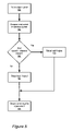
- FIG. 7 is a flowchart of one embodiment of a method of operating a voltage level generator.
- FIG. 8 is a schematic diagram of a diode simulator, according to one embodiment.
- FIG. 1 shows a diagram of a prior art temperature measurement unit 100 that determines the temperature of a diode-connected transistor, which may be located remotely from the unit.
- the voltage drop of a forward biased PN junction varies in a complementary fashion with respect to absolute temperature.
- a change in Vbe relative to a change in absolute temperature may be in the range of ⁇ 1 to ⁇ 1.5 millivolts per kelvin and linear to a first order approximation. This relationship may be referred to as complementary to absolute temperature (CTAT).
- CTAT complementary to absolute temperature
- the difference in the value of base-emitter voltage for a transistor operating at a first collector current density, J1, versus the value of Vbe when the transistor is operated at a second collector current density, J2, may be directly proportional to absolute temperature (PTAT).
- T q*(Vbe1 ⁇ Vbe2)/(k*ln(J1/J2))
- the temperature-measuring device of FIG. 1 may be constructed to measure the base-emitter voltage of transistor 150 operating first at one collector current density and then at a different collector current density, and then use the above relationship to calculate the corresponding value for temperature.
- a typical temperature-measuring device based on this principle may use a temperature sensing diode 150 located at the point where the temperature measurement is desired.
- a first known current may be applied to the diode by constant current source 110 and the corresponding voltage drop across the diode (V 120 minus V 130 ) may be recorded.
- a second known current may be applied to the diode by current source 110 and the corresponding voltage drop across the diode may again be recorded.
- the ratio of the collector current densities may be the same as the ratio of the applied currents. This ratio along with the two measurements for Vbe may be sufficient to solve the equation given above for absolute temperature, which may then be readily converted into any desired units of measure.
- the temperature sensing diode 150 In order to calibrate or determine the accuracy of a temperature measuring device such as the one described above, it may be typically necessary to place the temperature sensing diode 150 in an environmentally controlled chamber in which the temperature may be accurately measured and varied.
- the accuracy with which the temperature of the environment can be controlled and measured may determine the accuracy with which the temperature-measuring device can be tested or calibrated. For example, if an environmental chamber is capable of maintaining an internal temperature to within plus or minus one half degree, the accuracy of the temperature measuring device being calibrated may be somewhat less than this figure.
- the amount of time needed for an environmental chamber to reach a steady state temperature and for the device under test to achieve thermal equilibrium with the environment is typically quite large.
- the time required for a device under test to achieve thermal equilibrium with the environment of a typical thermal chamber after a change has been made to the desired temperature of the chamber may be on the order of several hours. Therefore, determining the accuracy of a temperature-measuring device at many points over a wide range of temperatures using prior art methods may be a very time-consuming undertaking.
- FIG. 2 illustrates a diode simulator 250 , according to one embodiment.
- Diode simulator 250 my pass the current supplied by current source 110 to diode-connected transistor 140 of the temperature measurement unit without modification. For example, if temperature measurement unit 100 supplies two levels of current to node 120 in a square wave pattern, diode simulator 250 may supply the same two levels of current in the same square wave pattern to node 130 of the temperature measurement unit. In response to desired temperature input 260 and the level of current being output by current source 110 of the temperature measurement unit, diode simulator 250 may output a voltage Vbe equal to V 120 minus V 130 corresponding to the base-emitter voltage of a diode-connected temperature-sensing transistor, which is independent of the temperature of the diode simulator 250 .
- desired test temperature input 260 may be established by a set of switches attached to diode simulator 250 . In other embodiments, desired test temperature input 260 may be supplied to diode simulator 250 from a personal computer or other device coupled to the simulator by an interconnect such as a bus.
- the output of diode simulator 250 may not depend upon its ambient temperature. Therefore, it may be used to calibrate temperature measurement unit 100 at any ambient temperature within its operational range regardless of the temperature to which the temperature measurement unit is to be calibrated. For example, if the ambient temperature of the facility in which the calibration is to be performed is 70 degrees F. and it is desired to calibrate temperature measurement unit 100 to a temperature of 100 degrees F., inputting data corresponding to 100 degrees F. on desired test temperature input 260 may cause the output of the diode simulator 250 to correspond to the voltage drop across a diode at 100 degrees F. Even if the ambient temperature of the facility in which the calibration is performed varies during the calibration procedure, the output of the diode simulator 250 may remain constant. These characteristics of the diode simulator may allow for calibration of a temperature measurement unit 100 in significantly less time than by using prior art methods, which include the requirement to tightly control the temperature of one or more system components.
- FIG. 3 shows a block diagram of the major components of diode simulator 350 , according to one embodiment.
- the function of current level detector 380 may be to sense the level of current being supplied by temperature measurement unit 300 to node 320 and to determine if the level is higher or lower than an internally generated reference current. It may also output the received current unmodified to node 330 and thence return it to the temperature measurement unit. In some embodiments, this may be accomplished by inserting a resistance in the current flow path to develop a voltage that is proportional to the received current and comparing the voltage thus developed to a reference voltage derived similarly from the reference current.
- current level detector 380 may generate a logic-level signal that is at logic 1 when the input current is at a high level and is at logic 0 when the input current is at a low level. Current level detector 380 may supply this logic signal to voltage generator 370 .
- Voltage level generator 370 may force a difference of potential, Vbe, between nodes 320 and 330 corresponding to the base-emitter voltage of a temperature-sensing, diode-connection transistor.
- voltage level generator 370 may force the voltage at node 320 to assume a value such that the difference of potential between nodes 320 and 330 approximates the voltage drop across a forward-biased PN junction.
- the voltage level generator 370 may force approximately 0.65 V difference of potential between nodes 320 and 330 .
- this voltage may be developed by passing a current through one or more resistors, such that the current multiplied by the resistance is equal to the desired difference of potential.
- voltage level generator 370 may force the voltage at node 320 to assume a value such that the difference of potential between nodes 320 and 330 approximates the voltage drop across a forward-biased PN junction plus and additional amount determined by the desired input temperature 360 .
- desired temperature input data received at 360 may be input to a digital to analog converter to produce a current proportional to the data. This current may be added to the current described previously and passed through the resistance to produce a difference of potential between nodes 320 and 330 equal to approximately 0.65V plus some delta V. Delta V may represent the change in base-emitter voltage of a diode-connected, temperature-sensing transistor attributable to the temperature of the transistor.
- the difference between the high reading and low reading may be the delta V produced by voltage level generator 370 corresponding to the data from the desired temperature input 360 .
- the desired input temperature data input to the diode simulator 350 may be compared to the temperature measurement output of the temperature measurement unit 300 to determine the accuracy of the temperature measurement reading independent of the temperature of the diode simulator.
- FIG. 4 illustrates a current level detector 450 , according to one embodiment.
- Temperature measurement unit 400 may deliver current at alternating levels of 10 and 170 micro Amperes from current source 410 to node 420 of the current level detector.
- Current source 455 may add a current between the low and high levels of current from the temperature measurement unit to node 420 . For example, current source 455 may add 100 uA to the input current at node 420 .
- Current sink 470 may draw the same amount of current through resistor 465 from node 420 as current source 455 adds.
- the current flowing from node 430 into diode-connected transistor 440 in the temperature measurement device may be exactly the same as that provided by current source 410 .
- a constant voltage drop may be generated from node 420 to the positive input of comparator 475 across resistor 465 by the 100 uA of current supplied by constant source 455 and removed by constant current sink 470 . Selecting the values of resistors 460 and 465 to be equal along with selecting the current through resistor 465 to be near the average of the high and low levels of input current from the temperature measurement unit may insure that when the input current is low the voltage drop across resistor 460 is smaller than that across resistor 465 . Since the voltage applied to comparator 475 is the difference between the voltage drops across resistors 465 and 460 , the voltage drop across resistor 465 may dominate and insure a negative voltage is applied to the comparator and thus a logic low (0) level for output signal 480 .
- the voltage drop across resistor 460 may be larger than that across resistor 465 . Since this voltage drop is negative with respect to the drop across resistor 465 , the difference between the two will be positive, providing a positive input voltage to comparator 475 and a logical high (1) level for output 480 . Therefore, the output 480 of the current level detector 450 may track the input current level from the temperature measurement unit 400 providing a logic 0 when the input current level is low and a logic 1 when the input current level is high. Note that this signal is generated without affecting the level of current input from the temperature measurement device as it flows into node 420 and is returned through node 430 .
- FIG. 5 is a flowchart for operating a current level detector, according to one embodiment.
- an input current may be received and passed through a resistance to produce a voltage drop proportional to the input current.
- a reference current generated internally to the current level detector may also passed through a resistance to produce a reference voltage, which is proportional to the reference current.
- the voltage drops produced may be in the same proportion to the currents from which they are derived, and their magnitudes may be compared directly, as shown at block 510 .
- the voltage derived from the input current may be applied to the negative input of a comparator while the voltage derived from the reference current is applied to the positive input of the comparator. In this fashion, the comparator may be able to determine whether the input current is greater than or less than the reference current, as illustrated by the decision block 520 .
- the comparator may output a logic 1 signal level when the magnitude of the input current is greater than that of the reference current, as indicated in block 530 , and may output a logic 0 signal level when the magnitude of the input current is less than that of the reference current, as shown in block 540 . In either case, the current level detector may return a current equal to the input current to the device under test, as illustrated by block 550 .
- FIG. 6 illustrates a voltage level generator 650 , according to one embodiment.
- Temperature measurement unit 600 may deliver current at alternating levels of 10 and 170 micro Amperes from current source 610 to node 620 of the voltage level generator. This current may pass through current level detector 690 and out to transistor 640 without alteration as described previously with respect to FIG. 4 .
- the digital-to-analog converter (DAC) enable signal from the current level detector 690 may track the input current level from temperature measurement unit 600 such that when the input current level is at 10 micro Amperes, the input signal is at logic 0, and when the input current level is at 170 micro Amperes, the input signal is at logic 1.
- DAC digital-to-analog converter
- the DAC enable signal may be used to gate the desired temperature input 660 to DAC 670 .
- DAC 670 may interpret its input as all zeros regardless of the state of desired temperature input bus 660 .
- DAC 670 may sink a current proportional to the value of its digital input through IO.
- DAC 670 may sink a current proportional to the complement of the value of its digital input through IOB. Therefore, the sum of the currents sunk by DAC 670 through IO and IOB may be constant.
- a constant current source may supply 200 micro Amperes of current to node 620 for the purpose of providing IO and IOB currents to DAC 670 .
- DAC 670 may interpret its desired temperature input as all zeros and sink no current through IO, while sinking 200 through IOB.
- Current source 655 may supply an additional 100 micro Amperes of current, which passes through resistors 665 and 675 to be sunk by constant current sink 680 .
- the values of resistors 665 and 675 may be selected such that the voltage drop from node 620 to node 630 when 100 micro Amperes of current is flowing through the resistors is approximately equal to the voltage drop across a diode-connected, temperature sensing transistor.
- DAC 670 may sense the data on desired temperature input bus 660 and output a current proportional to this value on IO. This current may flow through resistor 665 , and the resultant voltage drop may add to the voltage drop from node 620 to node 630 . Temperature measurement unit 600 may measure the increased voltage drop caused by DAC current through resistor 665 and interpret this as an indication of the temperature of a temperature-sensing diode.
- FIG. 7 is a flowchart of a method for operating a voltage level generator, according to one embodiment.
- data specifying a temperature for which diode characteristic simulation is desired may be received, along with an indication of the current level being output by the device under test, as shown in block 710 .
- decision block 720 if the input signal from the current level sensor is low, a low level of current may be generated, as shown at block 740 and passed through a resistance to develop a proportional output voltage, as indicated at 750 .
- the desired temperature input data may be used to generate a proportional current, as shown in block 730 , which may be added to the low-level current described previously.
- the composite current, thus generated, may be passed through a resistance to develop a proportional voltage drop, as indicated at block 750 .
- FIG. 8 is a schematic diagram of the components of a diode simulator, according to one embodiment. Multiple current sources are used in this circuit. Exemplary current sources for this application may include REF200 current sources from TI. Other exemplary components may include National Semiconductor's DAC0802 for the current DAC (U 3 ), Maxim's MAX4131 for the op amp (U 1 ) and MAX4190 for the comparator (U 2 ). Please note that all these parts may be replaced with comparable components.
- the eight-bit DAC has two complementary current outputs.
- IOB ((255 ⁇ T ⁇ 0:7>)/256)* I 1 (2)
- Seven of the eight address bits are brought out to the outside world and are used to command different delta V BE values. These seven bits are the seven LSBs of the DAC.
- the series of AND gates labeled U 4 enable the T ⁇ 0:6> address when the output of comparator U 2 is high and cause all DAC address bits to go low when the output of the comparator goes low.
- the MSB of the DAC is tied directly to the output of the comparator so that in all cases when the comparator is low its output is zero and when the comparator goes high the DAC MSB goes high.
- This programmable current is routed to the accurate 470 ⁇ resistor, R 2 , in the feedback path of op amp U 1 .
- the only path for this current to take is through R 2 since the other side of the 6 k ⁇ resistor (R 1 ) is connected to a 100 uA current source and the inverting input of the op amp (U 1 ), both of which are very high impedance.
- T ⁇ 0:6> are all low, the voltage developed across R 2 from the DAC0802 output, IO, is 0V when the comparator is low and 47.0 mV (470 ⁇ *100 uA) when the comparator is high.
- the operation of the op amp is as follows. With the output of the DAC, IO, equal to zero the current going through R 1 and R 2 is 100 uA provided by current source I 3 . Therefore, the voltage at the emitter of Q 1 (this is the anode voltage of the DUT) will be the voltage at the non-inverting input of the op amp plus (R 1 +R 2 )*100 uA.
- the voltage at the non-inverting input (this is the cathode connection to the DUT) of the op amp is the voltage generated by the diode internal to the DUT (Q 2 ), which is a function of the current through it. This voltage is typically 550 mV.
- V anode V cathode+100 uA*(6 k ⁇ +470 ⁇ ) ⁇ 1.2V This is the voltage desired because it is approximately equal to two diode drops that will occur with an external diode connected between the anode and cathode terminals of the DUT.
- I 2 provides 400 uA to the anode connection of the DUT. 199.2 uA of this current will always go to the DAC no matter what the T ⁇ 0:6> address is because IO and IOB both draw current off this node and, as stated earlier, the sum of these two currents is always 199.2 uA regardless what the DAC address is.
- Another 100 uA of this 400 uA current flows through the feedback resistors, R 1 and R 2 , to I 3 . This leaves 100.8 uA plus the switching current from the anode connection of the DUT to flow into Q 1 emitter and out its collector. 100 uA of this collector current flows through R 4 into I 4 , this develops ⁇ 130 mV across R 4 .
- the rest of the collector current (essentially the current from the switching current source of the DUT) flows through R 3 and into the cathode connection of the DUT, thus providing the same switching current to this port that would be there if an external diode was connected as in normal operation.
- the switching current through R 3 generates a switching voltage across R 3 with a low of ⁇ 221 mV (170 uA*1.3 k ⁇ ) and a high of ⁇ 13 mV (10 uA*1.3 k ⁇ ).
- This switching voltage drives the inverting input of comparator U 2 and the constant voltage of ⁇ 130 mV across R 4 drives the non-inverting input.
- the current out of the anode connection of the DUT is low (10 uA)
- the voltage at the inverting input of the comparator is higher than the voltage at the non-inverting input by 117 mV and the output of the comparator is low.
Abstract
Description
-
- where k=1.38×10⁻²³, Boltzmans constant
- T=absolute temperature in kelvins
- q=1.602×10⁻¹⁹, charge of an electron
- J1=the collector current density for Vbe1
- J2=the collector current density for Vbe2
- where k=1.38×10⁻²³, Boltzmans constant
-
- where k=1.38×10⁻²³, Boltzmans constant
- T=absolute temperature in kelvins
- q=1.602×10⁻¹⁹, charge of an electron
- J1=the collector current density for Vbe1
- J2=the collector current density for Vbe2
- where k=1.38×10⁻²³, Boltzmans constant
IO=(T<0:7>/256)*I 1 (1)
IOB=((255−T<0:7>)/256)*I 1 (2)
IO=((128+T<0:6>)/256)*200 uA. (3)
Where T<0:6> is the decimal representation of the seven bit binary input address.
ΔVBE=(kT/q)*ln(N) (4)
T=q*ΔVBE/(k*ln(N)) (5)
-
- T=absolute temperature in kelvins
- q=1.602×10⁻¹⁹, charge of an electron
- N=17, high to low current ratio for this design.
Using this equation, the range of temperatures that can be simulated with the DAC output current range and the 470 Ω resistor is: - For T<0:6>=0, minimum voltage shift
- ΔVBE=47.0 mV
- T=192.6° K=−80.4° C.
- For T<0:6>=127, maximum voltage shift
- ΔVBE=93.6 mV
- T=383.6° K=110.6° C.
Each LSB of the address changes the representative temperature by 1.5° C.
Vanode=Vcathode+100 uA*(6 kΩ+470 Ω)˜1.2V
This is the voltage desired because it is approximately equal to two diode drops that will occur with an external diode connected between the anode and cathode terminals of the DUT.
Vlow=Vcathode+100 uA*(6 kΩ+470 Ω)=Vcathode+647 mV
IO=((128+T<0:6>)/256)*200 uA
This current flows through R2 and the voltage at the anode is:
Vhigh=Vcathode+100 uA*(6 kΩ+470 Ω)+((128+T<0:6>)/256)* 200 uA)*470 Ω
Vhigh=Vcathode+647 mV+(((128+T<0:6>)/256)*200 uA)*470 Ω
T=q*ΔVBE/(k*ln(N))
ΔVBE=Vhigh−Vlow=Vcathode+647 mV+(((128+T<0:6>)/256)*200 uA)*470 Ω−(Vcathode+647 mV)
ΔVBE=(((128+T<0:6>)/256)*200 uA)*470 Ω
T=q*(((128+T<0:6>)/256)*200 uA)*470 Ω/(k*ln(17))
As shown earlier the temperature range that can be replicated with this circuit is −80.4° C. to 110.6° C.
Claims (11)
Priority Applications (1)
| Application Number | Priority Date | Filing Date | Title |
|---|---|---|---|
| US10/781,063 US7030793B2 (en) | 2004-02-18 | 2004-02-18 | Accurate testing of temperature measurement unit |
Applications Claiming Priority (1)
| Application Number | Priority Date | Filing Date | Title |
|---|---|---|---|
| US10/781,063 US7030793B2 (en) | 2004-02-18 | 2004-02-18 | Accurate testing of temperature measurement unit |
Publications (2)
| Publication Number | Publication Date |
|---|---|
| US20050179575A1 US20050179575A1 (en) | 2005-08-18 |
| US7030793B2 true US7030793B2 (en) | 2006-04-18 |
Family
ID=34838681
Family Applications (1)
| Application Number | Title | Priority Date | Filing Date |
|---|---|---|---|
| US10/781,063 Active 2024-06-30 US7030793B2 (en) | 2004-02-18 | 2004-02-18 | Accurate testing of temperature measurement unit |
Country Status (1)
| Country | Link |
|---|---|
| US (1) | US7030793B2 (en) |
Cited By (5)
| Publication number | Priority date | Publication date | Assignee | Title |
|---|---|---|---|---|
| US20070055473A1 (en) * | 2005-09-02 | 2007-03-08 | Standard Microsystems Corporation | EMI rejection for temperature sensing diodes |
| US20070146056A1 (en) * | 2005-11-22 | 2007-06-28 | Stmicroelectronics, Inc. | Temperature tamper detection circuit and method |
| US20070194813A1 (en) * | 2005-11-07 | 2007-08-23 | Washburn Robert D | Variable passive components with high resolution value selection and control |
| US20070237207A1 (en) * | 2004-06-09 | 2007-10-11 | National Semiconductor Corporation | Beta variation cancellation in temperature sensors |
| US9569641B2 (en) | 2015-03-24 | 2017-02-14 | Nxp Usa, Inc. | Data processing system with temperature monitoring for security |
Families Citing this family (8)
| Publication number | Priority date | Publication date | Assignee | Title |
|---|---|---|---|---|
| US7255476B2 (en) * | 2004-04-14 | 2007-08-14 | International Business Machines Corporation | On chip temperature measuring and monitoring circuit and method |
| US7484886B2 (en) * | 2006-05-03 | 2009-02-03 | International Business Machines Corporation | Bolometric on-chip temperature sensor |
| US7891865B2 (en) * | 2006-05-03 | 2011-02-22 | International Business Machines Corporation | Structure for bolometric on-chip temperature sensor |
| US9939335B2 (en) * | 2014-12-17 | 2018-04-10 | Nxp Usa, Inc. | Over-temperature detector with test mode |
| US10088861B2 (en) | 2016-11-21 | 2018-10-02 | Microsoft Technology Licensing, Llc | High accuracy voltage references |
| CN109655172A (en) * | 2019-01-25 | 2019-04-19 | 大连理工大学 | A kind of Pt100 thermal resistance sensor simulator based on reverse engineer |
| CN113494968B (en) * | 2020-03-19 | 2022-11-25 | 长鑫存储技术有限公司 | Temperature measurement and temperature calibration method and temperature measurement system |
| CN113280935B (en) * | 2021-07-21 | 2021-10-08 | 中国电子科技集团公司第九研究所 | Ferrite phase shifter magnetic core temperature detection device and detection method |
Citations (21)
| Publication number | Priority date | Publication date | Assignee | Title |
|---|---|---|---|---|
| US3672215A (en) | 1969-09-08 | 1972-06-27 | Worth Well Surveys Inc | Apparatus employing diode junction means for measuring subterranean temperatures |
| US3679992A (en) | 1971-06-01 | 1972-07-25 | Gen Electric | Tunnel diode oscillator fm temperature sensor |
| US4228684A (en) | 1979-06-04 | 1980-10-21 | General Motors Corporation | Remote temperature measuring system with semiconductor junction sensor |
| US4340882A (en) * | 1977-04-06 | 1982-07-20 | Nippon Telegraph And Telephone Public Corporation | D/A Conversion system with compensation circuit |
| US4636092A (en) | 1984-06-19 | 1987-01-13 | Hegyi Dennis J | Diode thermometer |
| US4958155A (en) * | 1989-01-31 | 1990-09-18 | Zdzislaw Gulczynski | Ultra fast digital-to-analog converter with independent bit current source calibration |
| EP0498799A1 (en) | 1989-11-04 | 1992-08-19 | Fraunhofer-Gesellschaft Zur Förderung Der Angewandten Forschung E.V. | Integratable temperature sensor circuit |
| US5195827A (en) | 1992-02-04 | 1993-03-23 | Analog Devices, Inc. | Multiple sequential excitation temperature sensing method and apparatus |
| US5419637A (en) | 1993-11-03 | 1995-05-30 | Santa Barbara Research Center | Method and apparatus for measuring temperature using an inherently calibrated p-n junction-type temperature sensor |
| GB2292221A (en) | 1994-08-09 | 1996-02-14 | Texas Instruments Ltd | Hottest temperature sensor |
| EP0741860A1 (en) | 1994-01-26 | 1996-11-13 | Horst Ahlers | Temperature sensor |
| US5982221A (en) | 1997-08-13 | 1999-11-09 | Analog Devices, Inc. | Switched current temperature sensor circuit with compounded ΔVBE |
| US6008685A (en) | 1998-03-25 | 1999-12-28 | Mosaic Design Labs, Inc. | Solid state temperature measurement |
| US6097239A (en) | 1999-02-10 | 2000-08-01 | Analog Devices, Inc. | Decoupled switched current temperature circuit with compounded ΔV be |
| US6246353B1 (en) * | 1999-09-13 | 2001-06-12 | Analog Devices, Inc. | Integrated-circuit structures and methods for correction of temperature and process-induced parameter errors |
| US6265857B1 (en) * | 1998-12-22 | 2001-07-24 | International Business Machines Corporation | Constant current source circuit with variable temperature compensation |
| US6480127B1 (en) * | 2001-09-27 | 2002-11-12 | National Semiconductor Corporation | Input sub-ranging converter system for sampling semiconductor temperature sensors |
| US6554470B2 (en) | 2000-11-07 | 2003-04-29 | Maxim Integrated Products, Inc. | M-level diode junction temperature measurement method cancelling series and parallel parasitic influences |
| US6554469B1 (en) | 2001-04-17 | 2003-04-29 | Analog Devices, Inc. | Four current transistor temperature sensor and method |
| US20040227651A1 (en) * | 2003-03-05 | 2004-11-18 | Shuji Furuichi | A/D conversion circuit, temperature-sens or circuit, integrated circuit, and method of adjusting the temperature-sensor circuit |
| US6933867B2 (en) * | 2003-11-12 | 2005-08-23 | Denso Corporation | A/D conversion processing apparatus providing improved elimination of effects of noise through digital processing, method of utilizing the A/D conversion processing apparatus, and electronic control apparatus incorporating the A/D conversion processing apparatus |
-
2004
- 2004-02-18 US US10/781,063 patent/US7030793B2/en active Active
Patent Citations (23)
| Publication number | Priority date | Publication date | Assignee | Title |
|---|---|---|---|---|
| US3672215A (en) | 1969-09-08 | 1972-06-27 | Worth Well Surveys Inc | Apparatus employing diode junction means for measuring subterranean temperatures |
| US3679992A (en) | 1971-06-01 | 1972-07-25 | Gen Electric | Tunnel diode oscillator fm temperature sensor |
| US4340882A (en) * | 1977-04-06 | 1982-07-20 | Nippon Telegraph And Telephone Public Corporation | D/A Conversion system with compensation circuit |
| US4228684A (en) | 1979-06-04 | 1980-10-21 | General Motors Corporation | Remote temperature measuring system with semiconductor junction sensor |
| US4636092A (en) | 1984-06-19 | 1987-01-13 | Hegyi Dennis J | Diode thermometer |
| DE3637520A1 (en) | 1985-06-18 | 1988-05-05 | Dennis J Hegyi | Temperature measuring device |
| US4958155A (en) * | 1989-01-31 | 1990-09-18 | Zdzislaw Gulczynski | Ultra fast digital-to-analog converter with independent bit current source calibration |
| EP0498799A1 (en) | 1989-11-04 | 1992-08-19 | Fraunhofer-Gesellschaft Zur Förderung Der Angewandten Forschung E.V. | Integratable temperature sensor circuit |
| US5195827A (en) | 1992-02-04 | 1993-03-23 | Analog Devices, Inc. | Multiple sequential excitation temperature sensing method and apparatus |
| US5419637A (en) | 1993-11-03 | 1995-05-30 | Santa Barbara Research Center | Method and apparatus for measuring temperature using an inherently calibrated p-n junction-type temperature sensor |
| EP0741860A1 (en) | 1994-01-26 | 1996-11-13 | Horst Ahlers | Temperature sensor |
| GB2292221A (en) | 1994-08-09 | 1996-02-14 | Texas Instruments Ltd | Hottest temperature sensor |
| US5982221A (en) | 1997-08-13 | 1999-11-09 | Analog Devices, Inc. | Switched current temperature sensor circuit with compounded ΔVBE |
| US6008685A (en) | 1998-03-25 | 1999-12-28 | Mosaic Design Labs, Inc. | Solid state temperature measurement |
| US6265857B1 (en) * | 1998-12-22 | 2001-07-24 | International Business Machines Corporation | Constant current source circuit with variable temperature compensation |
| US6097239A (en) | 1999-02-10 | 2000-08-01 | Analog Devices, Inc. | Decoupled switched current temperature circuit with compounded ΔV be |
| US6246353B1 (en) * | 1999-09-13 | 2001-06-12 | Analog Devices, Inc. | Integrated-circuit structures and methods for correction of temperature and process-induced parameter errors |
| US6554470B2 (en) | 2000-11-07 | 2003-04-29 | Maxim Integrated Products, Inc. | M-level diode junction temperature measurement method cancelling series and parallel parasitic influences |
| US6554469B1 (en) | 2001-04-17 | 2003-04-29 | Analog Devices, Inc. | Four current transistor temperature sensor and method |
| US6480127B1 (en) * | 2001-09-27 | 2002-11-12 | National Semiconductor Corporation | Input sub-ranging converter system for sampling semiconductor temperature sensors |
| US20040227651A1 (en) * | 2003-03-05 | 2004-11-18 | Shuji Furuichi | A/D conversion circuit, temperature-sens or circuit, integrated circuit, and method of adjusting the temperature-sensor circuit |
| US6956516B2 (en) * | 2003-03-05 | 2005-10-18 | Seiko Epson Corporation | A/D conversion circuit, temperature-sensor circuit, integrated circuit, and method of adjusting the temperature-sensor circuit |
| US6933867B2 (en) * | 2003-11-12 | 2005-08-23 | Denso Corporation | A/D conversion processing apparatus providing improved elimination of effects of noise through digital processing, method of utilizing the A/D conversion processing apparatus, and electronic control apparatus incorporating the A/D conversion processing apparatus |
Non-Patent Citations (5)
| Title |
|---|
| Cao Hui; Huang Junnai; "Circuit Design and Implementation for Digital Temperature and Humidity Measurement and Control," ASIC, 2001. Proceedings. 4th International Conference on Oct. 23-25, 2001, pp. 502-505. |
| Kaliyugavaradan, S.; Sankaran, P.; Murti, V.G.K.; "Application Of Reciprocal Time Generation Technique To Digital Temperature Measurement," IEEE Transactions on Instrumentation and Measurement, vol. 43, No. 1, Feb. 1994, pp. 99-100. |
| Michael P. Timko, "A Two-Terminal IC Temperature Tranducer", IEEE JSSC vol. SC-11, No. 6, Dec. 1976, pp. 784-788. |
| Shen-Whan Chen; Trung Duong; Min-Yih Luo; "Channel Temperature Measurement Using Pulse-Gate Method," IEEE Transactions on Microwave Theory and Techniques, vol. 47, No. 3, Mar. 1999, pp. 362-365. |
| Szajda et al. "A Low Noise, High Resolution Silicon Temperature Sensor", IEEE JSSC, vol. 31, No. 9, Sep. 1996, pp. 1308-1313. |
Cited By (11)
| Publication number | Priority date | Publication date | Assignee | Title |
|---|---|---|---|---|
| US20070237207A1 (en) * | 2004-06-09 | 2007-10-11 | National Semiconductor Corporation | Beta variation cancellation in temperature sensors |
| US7461974B1 (en) | 2004-06-09 | 2008-12-09 | National Semiconductor Corporation | Beta variation cancellation in temperature sensors |
| US20070055473A1 (en) * | 2005-09-02 | 2007-03-08 | Standard Microsystems Corporation | EMI rejection for temperature sensing diodes |
| US7622903B2 (en) * | 2005-09-02 | 2009-11-24 | Standard Microsystems Corporation | EMI rejection for temperature sensing diodes |
| US20070194813A1 (en) * | 2005-11-07 | 2007-08-23 | Washburn Robert D | Variable passive components with high resolution value selection and control |
| US7352312B2 (en) * | 2005-11-07 | 2008-04-01 | Washburn Robert D | Variable passive components with high resolution value selection and control |
| US20070146056A1 (en) * | 2005-11-22 | 2007-06-28 | Stmicroelectronics, Inc. | Temperature tamper detection circuit and method |
| US7362248B2 (en) * | 2005-11-22 | 2008-04-22 | Stmicroelectronics, Inc. | Temperature tamper detection circuit and method |
| US20080191917A1 (en) * | 2005-11-22 | 2008-08-14 | Stmicroelectronics, Inc. | Digital-to-analog converter circuit and method |
| US7724172B2 (en) | 2005-11-22 | 2010-05-25 | Stmicroelectronics, Inc. | Digital-to-analog converter circuit and method |
| US9569641B2 (en) | 2015-03-24 | 2017-02-14 | Nxp Usa, Inc. | Data processing system with temperature monitoring for security |
Also Published As
| Publication number | Publication date |
|---|---|
| US20050179575A1 (en) | 2005-08-18 |
Similar Documents
| Publication | Publication Date | Title |
|---|---|---|
| US7030793B2 (en) | Accurate testing of temperature measurement unit | |
| US9851402B2 (en) | Systems and methods mitigating temperature dependence of circuitry in electronic devices | |
| Nagarajan et al. | Improved single-element resistive sensor-to-microcontroller interface | |
| KR101258319B1 (en) | Method and device for providing linear relationship between temperature and digital code | |
| Krummenacher et al. | Smart temperature sensor in CMOS technology | |
| CN110243485B (en) | CMOS temperature sensor | |
| US6783274B2 (en) | Device for measuring temperature of semiconductor integrated circuit | |
| TWI396380B (en) | Accurate temperature measurement method for low beta transistors | |
| CN103674299A (en) | Circuit and method for determining temperature of transistor | |
| CN109791118B (en) | Measurement circuit for estimating resistance of resistive gas sensor | |
| US6946825B2 (en) | Bandgap voltage generator with a bipolar assembly and a mirror assembly | |
| KR100602888B1 (en) | A current source circuit and an autometic test equipment having the same | |
| Brokaw | A temperature sensor with single resistor set-point programming | |
| US11940831B2 (en) | Current generator for memory sensing | |
| Espejo et al. | MEDA Wind Sensor Front End ASIC | |
| US11940402B2 (en) | Circuit arrangement and sensor arrangements including the same | |
| US20230140251A1 (en) | High accuracy fast voltage and temperature sensor circuit | |
| Kunz | Exponential D/A converter with a dynamic range of eight decades | |
| US20200099384A1 (en) | Device and method for absolute voltage measurement | |
| JPH11304877A (en) | Voltage applying current measuring circuit | |
| CN114902412A (en) | Pin setting detection circuit | |
| RU2324908C2 (en) | Thermocouple signal simulator |
Legal Events
| Date | Code | Title | Description |
|---|---|---|---|
| AS | Assignment |
Owner name: STANDARD MICROSYSTEMS CORPORATION, NEW YORK Free format text: ASSIGNMENT OF ASSIGNORS INTEREST;ASSIGNORS:MCLEOD, SCOTT C.;CASTELLANO, WILLIAM;REEL/FRAME:014999/0445;SIGNING DATES FROM 20040115 TO 20040212 |
|
| STCF | Information on status: patent grant |
Free format text: PATENTED CASE |
|
| FPAY | Fee payment |
Year of fee payment: 4 |
|
| FPAY | Fee payment |
Year of fee payment: 8 |
|
| MAFP | Maintenance fee payment |
Free format text: PAYMENT OF MAINTENANCE FEE, 12TH YEAR, LARGE ENTITY (ORIGINAL EVENT CODE: M1553) Year of fee payment: 12 |
|
| AS | Assignment |
Owner name: MICROCHIP TECHNOLOGY INCORPORATED, ARIZONA Free format text: MERGER;ASSIGNOR:STANDARD MICROSYSTEMS CORPORATION;REEL/FRAME:044820/0715 Effective date: 20120501 |
|
| AS | Assignment |
Owner name: JPMORGAN CHASE BANK, N.A., AS ADMINISTRATIVE AGENT, DELAWARE Free format text: SECURITY INTEREST;ASSIGNORS:MICROCHIP TECHNOLOGY INC.;SILICON STORAGE TECHNOLOGY, INC.;ATMEL CORPORATION;AND OTHERS;REEL/FRAME:053311/0305 Effective date: 20200327 |
|
| AS | Assignment |
Owner name: SILICON STORAGE TECHNOLOGY, INC., ARIZONA Free format text: RELEASE BY SECURED PARTY;ASSIGNOR:JPMORGAN CHASE BANK, N.A, AS ADMINISTRATIVE AGENT;REEL/FRAME:053466/0011 Effective date: 20200529 Owner name: MICROCHIP TECHNOLOGY INC., ARIZONA Free format text: RELEASE BY SECURED PARTY;ASSIGNOR:JPMORGAN CHASE BANK, N.A, AS ADMINISTRATIVE AGENT;REEL/FRAME:053466/0011 Effective date: 20200529 Owner name: MICROSEMI STORAGE SOLUTIONS, INC., ARIZONA Free format text: RELEASE BY SECURED PARTY;ASSIGNOR:JPMORGAN CHASE BANK, N.A, AS ADMINISTRATIVE AGENT;REEL/FRAME:053466/0011 Effective date: 20200529 Owner name: ATMEL CORPORATION, ARIZONA Free format text: RELEASE BY SECURED PARTY;ASSIGNOR:JPMORGAN CHASE BANK, N.A, AS ADMINISTRATIVE AGENT;REEL/FRAME:053466/0011 Effective date: 20200529 Owner name: MICROSEMI CORPORATION, CALIFORNIA Free format text: RELEASE BY SECURED PARTY;ASSIGNOR:JPMORGAN CHASE BANK, N.A, AS ADMINISTRATIVE AGENT;REEL/FRAME:053466/0011 Effective date: 20200529 |
|
| AS | Assignment |
Owner name: WELLS FARGO BANK, NATIONAL ASSOCIATION, MINNESOTA Free format text: SECURITY INTEREST;ASSIGNORS:MICROCHIP TECHNOLOGY INC.;SILICON STORAGE TECHNOLOGY, INC.;ATMEL CORPORATION;AND OTHERS;REEL/FRAME:053468/0705 Effective date: 20200529 |
|
| AS | Assignment |
Owner name: WELLS FARGO BANK, NATIONAL ASSOCIATION, AS COLLATERAL AGENT, MINNESOTA Free format text: SECURITY INTEREST;ASSIGNORS:MICROCHIP TECHNOLOGY INCORPORATED;SILICON STORAGE TECHNOLOGY, INC.;ATMEL CORPORATION;AND OTHERS;REEL/FRAME:055671/0612 Effective date: 20201217 |
|
| AS | Assignment |
Owner name: WELLS FARGO BANK, NATIONAL ASSOCIATION, AS NOTES COLLATERAL AGENT, MINNESOTA Free format text: SECURITY INTEREST;ASSIGNORS:MICROCHIP TECHNOLOGY INCORPORATED;SILICON STORAGE TECHNOLOGY, INC.;ATMEL CORPORATION;AND OTHERS;REEL/FRAME:057935/0474 Effective date: 20210528 |
|
| AS | Assignment |
Owner name: MICROSEMI STORAGE SOLUTIONS, INC., ARIZONA Free format text: RELEASE BY SECURED PARTY;ASSIGNOR:WELLS FARGO BANK, NATIONAL ASSOCIATION, AS NOTES COLLATERAL AGENT;REEL/FRAME:059863/0400 Effective date: 20220228 Owner name: MICROSEMI CORPORATION, ARIZONA Free format text: RELEASE BY SECURED PARTY;ASSIGNOR:WELLS FARGO BANK, NATIONAL ASSOCIATION, AS NOTES COLLATERAL AGENT;REEL/FRAME:059863/0400 Effective date: 20220228 Owner name: ATMEL CORPORATION, ARIZONA Free format text: RELEASE BY SECURED PARTY;ASSIGNOR:WELLS FARGO BANK, NATIONAL ASSOCIATION, AS NOTES COLLATERAL AGENT;REEL/FRAME:059863/0400 Effective date: 20220228 Owner name: SILICON STORAGE TECHNOLOGY, INC., ARIZONA Free format text: RELEASE BY SECURED PARTY;ASSIGNOR:WELLS FARGO BANK, NATIONAL ASSOCIATION, AS NOTES COLLATERAL AGENT;REEL/FRAME:059863/0400 Effective date: 20220228 Owner name: MICROCHIP TECHNOLOGY INCORPORATED, ARIZONA Free format text: RELEASE BY SECURED PARTY;ASSIGNOR:WELLS FARGO BANK, NATIONAL ASSOCIATION, AS NOTES COLLATERAL AGENT;REEL/FRAME:059863/0400 Effective date: 20220228 |
|
| AS | Assignment |
Owner name: MICROSEMI STORAGE SOLUTIONS, INC., ARIZONA Free format text: RELEASE BY SECURED PARTY;ASSIGNOR:WELLS FARGO BANK, NATIONAL ASSOCIATION, AS NOTES COLLATERAL AGENT;REEL/FRAME:059363/0001 Effective date: 20220228 Owner name: MICROSEMI CORPORATION, ARIZONA Free format text: RELEASE BY SECURED PARTY;ASSIGNOR:WELLS FARGO BANK, NATIONAL ASSOCIATION, AS NOTES COLLATERAL AGENT;REEL/FRAME:059363/0001 Effective date: 20220228 Owner name: ATMEL CORPORATION, ARIZONA Free format text: RELEASE BY SECURED PARTY;ASSIGNOR:WELLS FARGO BANK, NATIONAL ASSOCIATION, AS NOTES COLLATERAL AGENT;REEL/FRAME:059363/0001 Effective date: 20220228 Owner name: SILICON STORAGE TECHNOLOGY, INC., ARIZONA Free format text: RELEASE BY SECURED PARTY;ASSIGNOR:WELLS FARGO BANK, NATIONAL ASSOCIATION, AS NOTES COLLATERAL AGENT;REEL/FRAME:059363/0001 Effective date: 20220228 Owner name: MICROCHIP TECHNOLOGY INCORPORATED, ARIZONA Free format text: RELEASE BY SECURED PARTY;ASSIGNOR:WELLS FARGO BANK, NATIONAL ASSOCIATION, AS NOTES COLLATERAL AGENT;REEL/FRAME:059363/0001 Effective date: 20220228 |
|
| AS | Assignment |
Owner name: MICROSEMI STORAGE SOLUTIONS, INC., ARIZONA Free format text: RELEASE BY SECURED PARTY;ASSIGNOR:WELLS FARGO BANK, NATIONAL ASSOCIATION, AS NOTES COLLATERAL AGENT;REEL/FRAME:060894/0437 Effective date: 20220228 Owner name: MICROSEMI CORPORATION, ARIZONA Free format text: RELEASE BY SECURED PARTY;ASSIGNOR:WELLS FARGO BANK, NATIONAL ASSOCIATION, AS NOTES COLLATERAL AGENT;REEL/FRAME:060894/0437 Effective date: 20220228 Owner name: ATMEL CORPORATION, ARIZONA Free format text: RELEASE BY SECURED PARTY;ASSIGNOR:WELLS FARGO BANK, NATIONAL ASSOCIATION, AS NOTES COLLATERAL AGENT;REEL/FRAME:060894/0437 Effective date: 20220228 Owner name: SILICON STORAGE TECHNOLOGY, INC., ARIZONA Free format text: RELEASE BY SECURED PARTY;ASSIGNOR:WELLS FARGO BANK, NATIONAL ASSOCIATION, AS NOTES COLLATERAL AGENT;REEL/FRAME:060894/0437 Effective date: 20220228 Owner name: MICROCHIP TECHNOLOGY INCORPORATED, ARIZONA Free format text: RELEASE BY SECURED PARTY;ASSIGNOR:WELLS FARGO BANK, NATIONAL ASSOCIATION, AS NOTES COLLATERAL AGENT;REEL/FRAME:060894/0437 Effective date: 20220228 |