US7088882B2 - Wavelength cross-connect - Google Patents
Wavelength cross-connect Download PDFInfo
- Publication number
- US7088882B2 US7088882B2 US10/493,109 US49310904A US7088882B2 US 7088882 B2 US7088882 B2 US 7088882B2 US 49310904 A US49310904 A US 49310904A US 7088882 B2 US7088882 B2 US 7088882B2
- Authority
- US
- United States
- Prior art keywords
- lenses
- array
- optical
- focal plane
- ports
- Prior art date
- Legal status (The legal status is an assumption and is not a legal conclusion. Google has not performed a legal analysis and makes no representation as to the accuracy of the status listed.)
- Expired - Lifetime, expires
Links
- 238000003491 array Methods 0.000 claims abstract description 30
- 230000003287 optical effect Effects 0.000 claims description 298
- 230000005540 biological transmission Effects 0.000 claims description 18
- 239000000758 substrate Substances 0.000 claims description 11
- 239000004973 liquid crystal related substance Substances 0.000 claims description 4
- GQYHUHYESMUTHG-UHFFFAOYSA-N lithium niobate Chemical compound [Li+].[O-][Nb](=O)=O GQYHUHYESMUTHG-UHFFFAOYSA-N 0.000 claims description 2
- 239000007787 solid Substances 0.000 claims description 2
- 239000006185 dispersion Substances 0.000 description 24
- 239000000835 fiber Substances 0.000 description 11
- 230000008878 coupling Effects 0.000 description 9
- 238000010168 coupling process Methods 0.000 description 9
- 238000005859 coupling reaction Methods 0.000 description 9
- 239000013307 optical fiber Substances 0.000 description 5
- 230000001419 dependent effect Effects 0.000 description 3
- 238000005516 engineering process Methods 0.000 description 3
- 239000011159 matrix material Substances 0.000 description 3
- 238000006243 chemical reaction Methods 0.000 description 2
- 230000004075 alteration Effects 0.000 description 1
- 230000008901 benefit Effects 0.000 description 1
- 230000002457 bidirectional effect Effects 0.000 description 1
- 239000003638 chemical reducing agent Substances 0.000 description 1
- 238000013461 design Methods 0.000 description 1
- 238000010586 diagram Methods 0.000 description 1
- 230000006872 improvement Effects 0.000 description 1
- 238000003780 insertion Methods 0.000 description 1
- 230000037431 insertion Effects 0.000 description 1
- 238000009533 lab test Methods 0.000 description 1
- 238000004519 manufacturing process Methods 0.000 description 1
- 239000012528 membrane Substances 0.000 description 1
- 238000000034 method Methods 0.000 description 1
- 230000008569 process Effects 0.000 description 1
Images


Classifications
-
- G—PHYSICS
- G02—OPTICS
- G02B—OPTICAL ELEMENTS, SYSTEMS OR APPARATUS
- G02B6/00—Light guides; Structural details of arrangements comprising light guides and other optical elements, e.g. couplings
- G02B6/10—Light guides; Structural details of arrangements comprising light guides and other optical elements, e.g. couplings of the optical waveguide type
- G02B6/12—Light guides; Structural details of arrangements comprising light guides and other optical elements, e.g. couplings of the optical waveguide type of the integrated circuit kind
- G02B6/12007—Light guides; Structural details of arrangements comprising light guides and other optical elements, e.g. couplings of the optical waveguide type of the integrated circuit kind forming wavelength selective elements, e.g. multiplexer, demultiplexer
- G02B6/12009—Light guides; Structural details of arrangements comprising light guides and other optical elements, e.g. couplings of the optical waveguide type of the integrated circuit kind forming wavelength selective elements, e.g. multiplexer, demultiplexer comprising arrayed waveguide grating [AWG] devices, i.e. with a phased array of waveguides
- G02B6/12011—Light guides; Structural details of arrangements comprising light guides and other optical elements, e.g. couplings of the optical waveguide type of the integrated circuit kind forming wavelength selective elements, e.g. multiplexer, demultiplexer comprising arrayed waveguide grating [AWG] devices, i.e. with a phased array of waveguides characterised by the arrayed waveguides, e.g. comprising a filled groove in the array section
-
- G—PHYSICS
- G02—OPTICS
- G02B—OPTICAL ELEMENTS, SYSTEMS OR APPARATUS
- G02B6/00—Light guides; Structural details of arrangements comprising light guides and other optical elements, e.g. couplings
- G02B6/10—Light guides; Structural details of arrangements comprising light guides and other optical elements, e.g. couplings of the optical waveguide type
- G02B6/12—Light guides; Structural details of arrangements comprising light guides and other optical elements, e.g. couplings of the optical waveguide type of the integrated circuit kind
- G02B6/12007—Light guides; Structural details of arrangements comprising light guides and other optical elements, e.g. couplings of the optical waveguide type of the integrated circuit kind forming wavelength selective elements, e.g. multiplexer, demultiplexer
- G02B6/12009—Light guides; Structural details of arrangements comprising light guides and other optical elements, e.g. couplings of the optical waveguide type of the integrated circuit kind forming wavelength selective elements, e.g. multiplexer, demultiplexer comprising arrayed waveguide grating [AWG] devices, i.e. with a phased array of waveguides
- G02B6/12019—Light guides; Structural details of arrangements comprising light guides and other optical elements, e.g. couplings of the optical waveguide type of the integrated circuit kind forming wavelength selective elements, e.g. multiplexer, demultiplexer comprising arrayed waveguide grating [AWG] devices, i.e. with a phased array of waveguides characterised by the optical interconnection to or from the AWG devices, e.g. integration or coupling with lasers or photodiodes
-
- G—PHYSICS
- G02—OPTICS
- G02B—OPTICAL ELEMENTS, SYSTEMS OR APPARATUS
- G02B6/00—Light guides; Structural details of arrangements comprising light guides and other optical elements, e.g. couplings
- G02B6/10—Light guides; Structural details of arrangements comprising light guides and other optical elements, e.g. couplings of the optical waveguide type
- G02B6/12—Light guides; Structural details of arrangements comprising light guides and other optical elements, e.g. couplings of the optical waveguide type of the integrated circuit kind
- G02B6/12007—Light guides; Structural details of arrangements comprising light guides and other optical elements, e.g. couplings of the optical waveguide type of the integrated circuit kind forming wavelength selective elements, e.g. multiplexer, demultiplexer
- G02B6/12009—Light guides; Structural details of arrangements comprising light guides and other optical elements, e.g. couplings of the optical waveguide type of the integrated circuit kind forming wavelength selective elements, e.g. multiplexer, demultiplexer comprising arrayed waveguide grating [AWG] devices, i.e. with a phased array of waveguides
- G02B6/12033—Light guides; Structural details of arrangements comprising light guides and other optical elements, e.g. couplings of the optical waveguide type of the integrated circuit kind forming wavelength selective elements, e.g. multiplexer, demultiplexer comprising arrayed waveguide grating [AWG] devices, i.e. with a phased array of waveguides characterised by means for configuring the device, e.g. moveable element for wavelength tuning
-
- G—PHYSICS
- G02—OPTICS
- G02B—OPTICAL ELEMENTS, SYSTEMS OR APPARATUS
- G02B6/00—Light guides; Structural details of arrangements comprising light guides and other optical elements, e.g. couplings
- G02B6/24—Coupling light guides
- G02B6/26—Optical coupling means
- G02B6/28—Optical coupling means having data bus means, i.e. plural waveguides interconnected and providing an inherently bidirectional system by mixing and splitting signals
- G02B6/293—Optical coupling means having data bus means, i.e. plural waveguides interconnected and providing an inherently bidirectional system by mixing and splitting signals with wavelength selective means
- G02B6/29304—Optical coupling means having data bus means, i.e. plural waveguides interconnected and providing an inherently bidirectional system by mixing and splitting signals with wavelength selective means operating by diffraction, e.g. grating
- G02B6/29305—Optical coupling means having data bus means, i.e. plural waveguides interconnected and providing an inherently bidirectional system by mixing and splitting signals with wavelength selective means operating by diffraction, e.g. grating as bulk element, i.e. free space arrangement external to a light guide
- G02B6/2931—Diffractive element operating in reflection
-
- G—PHYSICS
- G02—OPTICS
- G02B—OPTICAL ELEMENTS, SYSTEMS OR APPARATUS
- G02B6/00—Light guides; Structural details of arrangements comprising light guides and other optical elements, e.g. couplings
- G02B6/24—Coupling light guides
- G02B6/26—Optical coupling means
- G02B6/28—Optical coupling means having data bus means, i.e. plural waveguides interconnected and providing an inherently bidirectional system by mixing and splitting signals
- G02B6/293—Optical coupling means having data bus means, i.e. plural waveguides interconnected and providing an inherently bidirectional system by mixing and splitting signals with wavelength selective means
- G02B6/29304—Optical coupling means having data bus means, i.e. plural waveguides interconnected and providing an inherently bidirectional system by mixing and splitting signals with wavelength selective means operating by diffraction, e.g. grating
- G02B6/29305—Optical coupling means having data bus means, i.e. plural waveguides interconnected and providing an inherently bidirectional system by mixing and splitting signals with wavelength selective means operating by diffraction, e.g. grating as bulk element, i.e. free space arrangement external to a light guide
- G02B6/29311—Diffractive element operating in transmission
-
- G—PHYSICS
- G02—OPTICS
- G02B—OPTICAL ELEMENTS, SYSTEMS OR APPARATUS
- G02B6/00—Light guides; Structural details of arrangements comprising light guides and other optical elements, e.g. couplings
- G02B6/24—Coupling light guides
- G02B6/26—Optical coupling means
- G02B6/28—Optical coupling means having data bus means, i.e. plural waveguides interconnected and providing an inherently bidirectional system by mixing and splitting signals
- G02B6/293—Optical coupling means having data bus means, i.e. plural waveguides interconnected and providing an inherently bidirectional system by mixing and splitting signals with wavelength selective means
- G02B6/29304—Optical coupling means having data bus means, i.e. plural waveguides interconnected and providing an inherently bidirectional system by mixing and splitting signals with wavelength selective means operating by diffraction, e.g. grating
- G02B6/29305—Optical coupling means having data bus means, i.e. plural waveguides interconnected and providing an inherently bidirectional system by mixing and splitting signals with wavelength selective means operating by diffraction, e.g. grating as bulk element, i.e. free space arrangement external to a light guide
- G02B6/29313—Optical coupling means having data bus means, i.e. plural waveguides interconnected and providing an inherently bidirectional system by mixing and splitting signals with wavelength selective means operating by diffraction, e.g. grating as bulk element, i.e. free space arrangement external to a light guide characterised by means for controlling the position or direction of light incident to or leaving the diffractive element, e.g. for varying the wavelength response
-
- G—PHYSICS
- G02—OPTICS
- G02B—OPTICAL ELEMENTS, SYSTEMS OR APPARATUS
- G02B6/00—Light guides; Structural details of arrangements comprising light guides and other optical elements, e.g. couplings
- G02B6/24—Coupling light guides
- G02B6/26—Optical coupling means
- G02B6/35—Optical coupling means having switching means
- G02B6/354—Switching arrangements, i.e. number of input/output ports and interconnection types
- G02B6/356—Switching arrangements, i.e. number of input/output ports and interconnection types in an optical cross-connect device, e.g. routing and switching aspects of interconnecting different paths propagating different wavelengths to (re)configure the various input and output links
-
- H—ELECTRICITY
- H04—ELECTRIC COMMUNICATION TECHNIQUE
- H04Q—SELECTING
- H04Q11/00—Selecting arrangements for multiplex systems
- H04Q11/0001—Selecting arrangements for multiplex systems using optical switching
- H04Q11/0005—Switch and router aspects
-
- G—PHYSICS
- G02—OPTICS
- G02B—OPTICAL ELEMENTS, SYSTEMS OR APPARATUS
- G02B6/00—Light guides; Structural details of arrangements comprising light guides and other optical elements, e.g. couplings
- G02B6/24—Coupling light guides
- G02B6/26—Optical coupling means
- G02B6/28—Optical coupling means having data bus means, i.e. plural waveguides interconnected and providing an inherently bidirectional system by mixing and splitting signals
- G02B6/293—Optical coupling means having data bus means, i.e. plural waveguides interconnected and providing an inherently bidirectional system by mixing and splitting signals with wavelength selective means
- G02B6/29379—Optical coupling means having data bus means, i.e. plural waveguides interconnected and providing an inherently bidirectional system by mixing and splitting signals with wavelength selective means characterised by the function or use of the complete device
- G02B6/2938—Optical coupling means having data bus means, i.e. plural waveguides interconnected and providing an inherently bidirectional system by mixing and splitting signals with wavelength selective means characterised by the function or use of the complete device for multiplexing or demultiplexing, i.e. combining or separating wavelengths, e.g. 1xN, NxM
- G02B6/29382—Optical coupling means having data bus means, i.e. plural waveguides interconnected and providing an inherently bidirectional system by mixing and splitting signals with wavelength selective means characterised by the function or use of the complete device for multiplexing or demultiplexing, i.e. combining or separating wavelengths, e.g. 1xN, NxM including at least adding or dropping a signal, i.e. passing the majority of signals
-
- G—PHYSICS
- G02—OPTICS
- G02B—OPTICAL ELEMENTS, SYSTEMS OR APPARATUS
- G02B6/00—Light guides; Structural details of arrangements comprising light guides and other optical elements, e.g. couplings
- G02B6/24—Coupling light guides
- G02B6/26—Optical coupling means
- G02B6/35—Optical coupling means having switching means
- G02B6/351—Optical coupling means having switching means involving stationary waveguides with moving interposed optical elements
- G02B6/3512—Optical coupling means having switching means involving stationary waveguides with moving interposed optical elements the optical element being reflective, e.g. mirror
-
- G—PHYSICS
- G02—OPTICS
- G02B—OPTICAL ELEMENTS, SYSTEMS OR APPARATUS
- G02B6/00—Light guides; Structural details of arrangements comprising light guides and other optical elements, e.g. couplings
- G02B6/24—Coupling light guides
- G02B6/26—Optical coupling means
- G02B6/35—Optical coupling means having switching means
- G02B6/351—Optical coupling means having switching means involving stationary waveguides with moving interposed optical elements
- G02B6/3524—Optical coupling means having switching means involving stationary waveguides with moving interposed optical elements the optical element being refractive
- G02B6/3526—Optical coupling means having switching means involving stationary waveguides with moving interposed optical elements the optical element being refractive the optical element being a lens
-
- G—PHYSICS
- G02—OPTICS
- G02B—OPTICAL ELEMENTS, SYSTEMS OR APPARATUS
- G02B6/00—Light guides; Structural details of arrangements comprising light guides and other optical elements, e.g. couplings
- G02B6/24—Coupling light guides
- G02B6/26—Optical coupling means
- G02B6/35—Optical coupling means having switching means
- G02B6/351—Optical coupling means having switching means involving stationary waveguides with moving interposed optical elements
- G02B6/3524—Optical coupling means having switching means involving stationary waveguides with moving interposed optical elements the optical element being refractive
- G02B6/3528—Optical coupling means having switching means involving stationary waveguides with moving interposed optical elements the optical element being refractive the optical element being a prism
-
- G—PHYSICS
- G02—OPTICS
- G02B—OPTICAL ELEMENTS, SYSTEMS OR APPARATUS
- G02B6/00—Light guides; Structural details of arrangements comprising light guides and other optical elements, e.g. couplings
- G02B6/24—Coupling light guides
- G02B6/26—Optical coupling means
- G02B6/35—Optical coupling means having switching means
- G02B6/351—Optical coupling means having switching means involving stationary waveguides with moving interposed optical elements
- G02B6/3534—Optical coupling means having switching means involving stationary waveguides with moving interposed optical elements the optical element being diffractive, i.e. a grating
-
- H—ELECTRICITY
- H04—ELECTRIC COMMUNICATION TECHNIQUE
- H04J—MULTIPLEX COMMUNICATION
- H04J14/00—Optical multiplex systems
- H04J14/02—Wavelength-division multiplex systems
- H04J14/0201—Add-and-drop multiplexing
- H04J14/0202—Arrangements therefor
- H04J14/021—Reconfigurable arrangements, e.g. reconfigurable optical add/drop multiplexers [ROADM] or tunable optical add/drop multiplexers [TOADM]
- H04J14/0212—Reconfigurable arrangements, e.g. reconfigurable optical add/drop multiplexers [ROADM] or tunable optical add/drop multiplexers [TOADM] using optical switches or wavelength selective switches [WSS]
-
- H—ELECTRICITY
- H04—ELECTRIC COMMUNICATION TECHNIQUE
- H04Q—SELECTING
- H04Q11/00—Selecting arrangements for multiplex systems
- H04Q11/0001—Selecting arrangements for multiplex systems using optical switching
- H04Q11/0005—Switch and router aspects
- H04Q2011/0007—Construction
- H04Q2011/0016—Construction using wavelength multiplexing or demultiplexing
-
- H—ELECTRICITY
- H04—ELECTRIC COMMUNICATION TECHNIQUE
- H04Q—SELECTING
- H04Q11/00—Selecting arrangements for multiplex systems
- H04Q11/0001—Selecting arrangements for multiplex systems using optical switching
- H04Q11/0005—Switch and router aspects
- H04Q2011/0007—Construction
- H04Q2011/0026—Construction using free space propagation (e.g. lenses, mirrors)
- H04Q2011/003—Construction using free space propagation (e.g. lenses, mirrors) using switches based on microelectro-mechanical systems [MEMS]
-
- H—ELECTRICITY
- H04—ELECTRIC COMMUNICATION TECHNIQUE
- H04Q—SELECTING
- H04Q11/00—Selecting arrangements for multiplex systems
- H04Q11/0001—Selecting arrangements for multiplex systems using optical switching
- H04Q11/0005—Switch and router aspects
- H04Q2011/0007—Construction
- H04Q2011/0032—Construction using static wavelength routers (e.g. arrayed waveguide grating router [AWGR] )
Definitions
- This invention relates to the field of DWDM fiber optics telecommunications and in particular to the field of all-optical switching.
- a typical all-optical switch would consist of a large core all-optical switch matrix surrounded by DWDM demultiplexers and multiplexers at each fibre interface.
- Large optical switching matrices are hard to fabricate, complex to control, require overwhelming fibre management and are very expensive.
- a wavelength selective all-optical switch is called a wavelength selective cross-connect WSXC (R. E. Wagner, Journal of Lightwave Technology, Vol. 14, No. 6, June 1996, also U.S. Pat. No. 6,097,859) by Solgaard et al.
- WSXC wavelength selective cross-connect
- Such a device generally has N incoming fibres and N outgoing fibres, each fibre being capable of transporting M wavelength channels.
- the WXC enables independent switching of each of the M wavelength channels from the N incoming fibres to the N outgoing fibres. It is functionally equivalent to an input array of N wavelength demultiplexers routed to an output array of N wavelength multiplexers through an array of M N ⁇ N optical switches.
- the invention provides a wavelength cross connect comprising: a first plurality of lenses stacked vertically; a second plurality of lenses stacked vertically, spaced from said first plurality of lenses, non-overlapping in vertical space with said first plurality of lenses; a first plurality of dispersive elements, with one dispersive element substantially in a first focal plane of each of said first plurality of lenses; a second plurality of dispersive elements, with one dispersive element substantially in a second focal plane of each of said second plurality of lenses; a first array of switching elements controllable in two directions, the first array being substantially in a second focal plane of each of said first plurality of lenses; a second array of switching elements controllable in two directions, the second array being substantially in a first focal plane of each of said second plurality of lenses; in a first plurality of optical ports a respective optical port positioned to input light onto/receive light from each of said first plurality of lenses; in a second plurality of optical ports a respective optical port positioned to
- the switching elements are MEMS switching elements.
- each first bulk optical element is selected from a group consisting of a lens or a curved mirror.
- the dispersive element is selected from a group consisting of: a diffraction grating, either reflection and transmission type, prisms.
- the invention provides a wavelength cross connect comprising: a first plurality of lenses stacked vertically; a second plurality of lenses stacked vertically, spaced from said first plurality of lenses, non-overlapping in vertical space with said first plurality of lenses; a first dispersive element at least part of which is substantially in a first focal plane of each of said first plurality of lenses; a second dispersive element at least part of which is substantially in a second focal plane of each of said second plurality of lenses; a first array of switching elements controllable in two directions, the first array being substantially in a second focal plane of each of said first plurality of lenses; a second array of switching elements controllable in two directions, the second array being substantially in a first focal plane of each of said second plurality of lenses; in a first plurality of optical ports a respective optical port positioned to input light onto/receive light from each of said first plurality of lenses; in a second plurality of optical ports a respective optical port positioned to input light onto/receive light
- the switching elements are MEMS switching elements.
- each first bulk optical element is selected from a group consisting of a lens or a curved mirror.
- the dispersive element is selected from a group consisting of: a diffraction grating, either reflection and transmission type, prisms.
- the invention provides a wavelength cross connect comprising: a first plurality of lenses stacked vertically; a second plurality of lenses stacked vertically, spaced from said first plurality of lenses, non-overlapping in vertical space with said first plurality of lenses; a first plurality of dispersive elements, with one dispersive element substantially in a first focal plane of each of said first plurality of lenses; a second plurality of dispersive elements, with one dispersive element substantially in a second focal plane of each of said second plurality of lenses; a first array of transmissive switching elements controllable in two directions, the first array being substantially in a second focal plane of each of said first plurality of lenses; a second array of transmissive switching elements controllable in two directions, the second array being substantially in a first focal plane of each of said second plurality of lenses; in a first plurality of optical ports a respective optical port positioned to input light onto/receive light from each of said first plurality of lenses; in a second plurality of optical ports a
- the transmissive switching elements are one of a liquid crystal beam steering element, an acousto-optic beam deflector, part of a solid state phase array, a controllable hologram, and a periodically poled Lithium Niobate beam deflector.
- each first bulk optical element is selected from a group consisting of a lens or a curved mirror.
- the dispersive element is selected from a group consisting of: a diffraction grating, either reflection and transmission type, prisms.
- the invention provides a wavelength cross connect comprising: a first plurality of lenses stacked vertically; a second plurality of lenses stacked vertically, spaced from said first plurality of lenses, non-overlapping in vertical space with said first plurality of lenses; a first plurality of dispersive elements, with one dispersive element substantially in a first focal plane of each of said first plurality of lenses; a second plurality of dispersive elements, with one dispersive element substantially in a second focal plane of each of said second plurality of lenses; a first array of switching elements controllable in two directions, the first array being substantially in a second focal plane of each of said first plurality of lenses; a second array of switching elements controllable in two directions, the second array being substantially in a first focal plane of each of said second plurality of lenses; a first two dimensional array of optical ports; a second two dimensional array of optical ports; for each row of said first two dimensional array of optical ports, a respective first bulk optical element having optical power and having a fourth focal
- the switching elements are MEMS switching elements.
- each bulk optical element is a lens or a curved mirror.
- the dispersive element is selected from a group comprising: a diffraction grating, either reflection and transmission type, prisms.
- the invention provides a wavelength cross connect comprising: a first plurality of lenses stacked vertically; a second plurality of lenses stacked vertically, spaced from said first plurality of lenses, non-overlapping in vertical space with said first plurality of lenses; a first plurality of dispersive elements, with one dispersive element substantially in a first focal plane of each of said first plurality of lenses; a second plurality of dispersive elements, with one dispersive element substantially in a second focal plane of each of said second plurality of lenses; a first array of switching elements controllable in two directions, the first array being substantially in a second focal plane of each of said first plurality of lenses; a second array of switching elements controllable in two directions, the second array being substantially in a first focal plane of each of said second plurality of lenses; a first two dimensional array of optical ports; a second two dimensional array of optical ports; a first bulk optical element having optical power and having a fourth focal plane substantially coplanar with said first focal plane of said second plurality
- the switching elements are MEMS switching elements.
- each bulk optical element is a lens or a curved mirror.
- the dispersive element is selected from a group comprising: a diffraction grating, either reflection and transmission type, prisms.
- the invention provides an arrangement comprising: a first two dimensional array of optical ports; a first two dimensional array of waveguide dispersive elements on a plurality of waveguide substrates, with one waveguide dispersive element per optical port in said first two dimensional array of optical ports, the first two dimensional array of waveguide dispersive elements collectively having a first output plane; for each row of said first two dimensional array of optical ports, a respective first bulk optical element having optical power and having a first focal plane substantially coplanar with said first output plane, and having a second focal plane; a first array of switching elements substantially in the second focal plane, each switching element being adapted to switch in both a horizontal and vertical direction; a second two dimensional array of optical ports; a second two dimensional array of waveguide dispersive elements on a plurality of waveguide substrates, with one waveguide dispersive element per optical port in said second two dimensional array of optical ports, the second two dimensional array of waveguide dispersive elements collectively having a second output plane; for
- the switching elements are MEMS switching elements.
- each bulk optical element having optical power is a lens or a curved mirror.
- the dispersive elements comprise arrayed waveguide gratings or Echelle gratings.
- the invention provides an arrangement comprising: a first two dimensional array of optical ports; a first two dimensional array of waveguide dispersive elements on a plurality of waveguide substrates, with one waveguide dispersive element per optical port in said first two dimensional array of optical ports, the first two dimensional array of waveguide dispersive elements collectively having a first output plane; a first bulk optical element having optical power and having a first focal plane substantially coplanar with said first output plane, and having a second focal plane; a first array of switching elements substantially in the second focal plane, each switching element being adapted to switch in both a horizontal and vertical direction; a second two dimensional array of optical ports; a second two dimensional array of waveguide dispersive elements on a plurality of waveguide substrates, with one waveguide dispersive element per optical port in said second two dimensional array of optical ports, the second two dimensional array of waveguide dispersive elements collectively having a second output plane; a second bulk optical element having optical power and having a fifth focal plane
- the switching elements are MEMS switching elements.
- each bulk optical element having optical power is a lens or a curved mirror.
- the dispersive elements comprise arrayed waveguide gratings or Echelle gratings.
- the invention provides a wavelength cross connect comprising: a first plurality of lenses stacked vertically; a second plurality of lenses stacked vertically, spaced from said first plurality of lenses, non-overlapping in vertical space with said first plurality of lenses; a first plurality of dispersive elements, with one dispersive element substantially in a first focal plane of each of said first plurality of lenses; a second plurality of dispersive elements, with one dispersive element substantially in a second focal plane of each of said second plurality of lenses; a first array of transmissive switching elements controllable in two directions, the first array being substantially in a second focal plane of each of said first plurality of lenses; a second array of transmissive switching elements controllable in two directions, the second array being substantially in a first focal plane of each of said second plurality of lenses; a first two dimensional array of optical ports; a second two dimensional array of optical ports; for each row of said first two dimensional array of optical ports, a respective first bulk optical element having optical power
- each bulk optical element a lens or a curved mirror.
- the dispersive element is selected from a group comprising: a diffraction grating, either reflection and transmission type, prisms.
- the invention provides a wavelength cross connect comprising: a first plurality of lenses stacked vertically; a second plurality of lenses stacked vertically, spaced from said first plurality of lenses, non-overlapping in vertical space with said first plurality of lenses; a first plurality of dispersive elements, with one dispersive element substantially in a first focal plane of each of said first plurality of lenses; a second plurality of dispersive elements, with one dispersive element substantially in a second focal plane of each of said second plurality of lenses; a first array of transmissive switching elements controllable in two directions, the first array being substantially in a second focal plane of each of said first plurality of lenses; a second array of transmissive switching elements controllable in two directions, the second array being substantially in a first focal plane of each of said second plurality of lenses; a first two dimensional array of optical ports; a second two dimensional array of optical ports; a first bulk optical element having optical power and having a fourth focal plane substantially coplanar with said first focal
- each bulk optical element a lens or a curved mirror.
- the dispersive element is selected from a group comprising: a diffraction grating, either reflection and transmission type, prisms.
- the invention provides an arrangement comprising: a first plurality of lenses stacked vertically; a second plurality of lenses stacked vertically, spaced from said first plurality of lenses, non-overlapping in vertical space with said first plurality of lenses; a first plurality of dispersive elements, with one dispersive element substantially in a first focal plane of each of said first plurality of lenses; a second plurality of dispersive elements, with one dispersive element substantially in a second focal plane of each of said second plurality of lenses; a first array of switching elements controllable in two directions, the first array being substantially in a second focal plane of each of said first plurality of lenses; a second array of switching elements controllabe in two directions, the second array being substantially in a first focal plane of each of said second plurality of lenses; a first plurality of two dimensional arrays of optical ports; a second plurality of two dimensional arrays of optical ports; for each two dimensional array of said first plurality of two dimensional arrays of optical ports, a respective first
- the switching elements are MEMS switching elements.
- the switching elements are transmissive.
- each bulk optical element is selected from a group consisting of a lens, a curved mirror, an assembly of lenses and mirrors, and an assembly of lenses, mirrors and a curved mirror.
- the second bulk optical element is selected from a group consisting of a lens, a curved mirror, an assembly of lenses and mirrors, and an assembly of lenses, mirrors and a curved mirror.
- the dispersive element is selected from a group comprising: a diffraction grating, either reflection and transmission type, prisms.
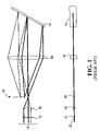
- FIG. 1 shows top and side views of a conventional wavelength switch configured as a 1 ⁇ 5 wavelength selective switch using free-space optics and MEMS switching elements;
- FIG. 2 shows top and side views of a ROADM with large number of add/drop ports configured as a 1 ⁇ 25 wavelength selective switch using free-space optics and MEMS switching elements;
- FIG. 3 shows a perspective view of the ROADM of FIG. 2 ;
- FIG. 4 shows top and side views of a ROADM provided with a large number of add/drop ports configured as a 1 ⁇ 25 wavelength selective switch using waveguide optics and MEMS switching elements;
- FIG. 5 shows a wavelength cross-connect arrangement using free-space optics and MEMS switching elements, provided by an embodiment of the invention
- FIG. 6A shows top and side views of a WXC/ROADM device provided by an embodiment of the invention using free-space optics and MEMS switching elements, in which each optical port has 5 local add/drop ports;
- FIG. 6B shows the add/drop/switch function of the device of FIG. 6A ;
- FIG. 7 shows a perspective view of the elements of the embodiment shown in FIG. 8 ;
- FIG. 8 shows top and side views of a WXC/ROADM device provided by an embodiment of the invention using waveguide optics and MEMS switching elements, in which each optical port has 5 local add/drop ports;
- FIG. 9 shows top and side views of a WXC/ROADM provided by an embodiment of the invention with a large number of add/drop ports device using free-space optics and MEMS switching elements, in which each optical port has 25 local add/drop ports;
- FIG. 10 shows top and side views of a WXC/ROADM provided by an embodiment of the invention with a large number of add/drop ports device using waveguide optics and MEMS switching elements, in which each optical port has 25 local add/drop ports;
- FIG. 11 shows top and side views of another embodiment of a WXC/ROADM device as per the invention using transmissive switching elements and waveguide optics, in which each optical port has 5 local add/drop ports.
- wavelength dispersion can be realized through diffraction gratings (both reflection and transmission type) or prisms in free-space embodiments or through arrayed waveguide gratings or Echelle gratings in waveguide embodiments.
- Bulk optical elements having optical powers can be any of a lens, a curved mirror, or any suitable combination of optical elements, either spherical or cylindrical, that provide the appropriate optical function.
- the array of switching means can be either reflective (mirrors, tunable gratings, interferometric arrangements of fixed and movable membranes, etc.), with the best mode being micro-mirror arrays fabricated through micro-fabrication processes, or transmissive (liquid crystal, electro-holograms, optical phase arrays, tiltable micro-prisms or movable micro-lenses, etc.).
- An example of a liquid crystal based switch is shown in: Patel et al., Photonics Technology Letters, Vol. 7, No. 5, May 1995. Waveguide and free space embodiments are possible to perform each of the dispersion and optical coupling steps, and any arbitrary appropriate combination can be employed.
- top part of each figure shows a top view, also referred to as the dispersion plane due to the choice of orientation of the dispersive elements, while the bottom part of the figure shows the side view.
- FIG. 1 shows a known wavelength switch taught in D. M. Marom et al., Optical Fibre Communications conference, PD FB 7 , Anaheim, 2002. It is configured as a 1 ⁇ 5 with MEMS switching elements.
- a group of 5 optical ports 10 is provided in the form of a linear array of optical fibres coupled to an array of micro-lenses 12 used to substantially collimate/focus the light beams from/to the optical fibres.
- the middle fibre is used as an input port, while the 4 others are used as outputs, although light paths going from the middle fibre back to the middle fibre are possible when used in conjunction with an optical circulator (thus the denomination as a 1 ⁇ 5 arrangement).
- a light beam containing multiple wavelengths is input through the middle optical port, is collimated by the middle micro-lens and is directed to a diffraction grating 14 through a telescope arrangement consisting of a coupling lens 16 and a main lens 18 .
- the light beam After reflecting from the diffraction grating 14 , the light beam is demultiplexed into a plurality of wavelength channels, each impinging on a corresponding MEMS switch element 20 .
- This MEMS can tilt in the plane of the dispersion to route the wavelength channels to alternate locations on the diffraction grating 14 .
- the images of these alternate locations through the telescope can be made to precisely align to one of the micro-lens, thus the wavelength channels is made to couple to a selectable optical port.
- FIG. 2 shows a wavelength switch providing a large number of optical ports that can be used for example as a ROADM with a large number of add/drop ports.
- the wavelength switch can be configured as a 1 ⁇ 25. This is a variant of a system taught in U.S. Pat. No. 6,549,699 to Belser et al.
- This dramatic increase in scalability in number of ports is achieved by using a two dimensional arrangement of optical ports consisting of a two dimensional array of fibres 30 connected to a two dimensional array of micro-lenses 32 to substantially collimate/focus light beams as they emerged/are coupled to the optical fibres and by using an array of MEMS switching elements 34 capable of directing light beams in both the plane of dispersion and the plane perpendicular to the plane of dispersion.
- the ports are arranged in a 5 ⁇ 5 array, enabling one input and 25 potential outputs, thus the 1 ⁇ 25 naming (counting the path from the input back to itself as one possible path, although requiring an external circulator).
- a light beam containing multiple wavelengths is input through the middle optical port, is collimated by the middle micro-lens and is directed to the diffraction through a telescope arrangement consisting of a coupling lens 36 and a main lens 38 .
- the light beam After reflecting from a diffraction grating, the light beam is demultiplexed into a plurality of wavelength channels, each impinging on a corresponding MEMS switch element 34 .
- This MEMS can tilt both in the plane of the dispersion and in the plane perpendicular to the dispersion plane to route the wavelength channels to alternate locations on the diffraction grating 40 .
- the images of these alternate locations through the telescope can be made to precisely align to one of the micro-lens of the two dimensional array 32 , thus each wavelength channel is made to couple to a selectable optical port.
- a wavelength channel is an arbitrary contiguous frequency band.
- a single wavelength channel might include one or more ITU wavelengths and intervening wavelengths for example.
- ⁇ is referred to herein in respect of a wavelength channel, this is not intended to imply a wavelength channel is a single wavelength only.
- the image formed on the grating 40 containing all possible alternate locations is small both in the dispersion plane and in the plane perpendicular to the dispersion plane.
- the width of the image in the plane of dispersion would be reduced by a factor of 6, which has a dramatic impact on optical performances of the system.
- the larger size of the embodiment as per the invention in the plane perpendicular to the dispersion plane has a small negative impact since the system remains mostly on-axis in that plane.
- the two,dimensional arrangement of optical ports provided by the invention would enable building a device of up to 1 ⁇ 64 ports or with a smaller number of ports but with improved optical performances and smaller size. These numerical values are for the purpose of explaining the improvement over the FIG. 1 arrangement. Other numbers of ports are possible.
- FIG. 3 shows a perspective view. The two dimensional arrangement of ports and corresponding micro-lenses is clearly visible on this drawing.
- FIG. 4 shows another embodiment as per co-application 50088-4 performing a similar function that the device shown on FIG. 3 , but using waveguide based dispersive elements.
- FIG. 5 shows a wavelength cross-connect arrangement using free-space optics and MEMS switching elements provided by an embodiment of the invention. It basically consists of a first stack 54 , 56 , 58 , 60 and a second stack 62 , 64 , 66 , 68 of dispersive arrangements connected together via optical paths established by MEMS micro-mirrors capable of tilting in the plane perpendicular to the dispersion plane. More specifically, referring to the bottom view of FIG. 5 , there are four input ports 42 , 43 , 44 , 45 and four output ports 46 , 47 , 48 , 49 . This designation between input and output is arbitrary, and any port can function as either input or output.
- Each input port 42 , 43 , 44 , 45 has a respective main lens 80 , 82 , 84 , 86 through which light travels on the way to a respective diffraction grating 62 , 64 , 66 , 68 .
- Each diffraction grating 62 , 64 , 66 , 68 redirects light back through the respective main lens 80 , 82 , 84 , 86 to a respective array of MEMS micro-mirrors 88 , 90 , 92 , 94 .
- Each array of MEMS micro-mirrors for example array 88 shown in the top view, includes a series of micro-mirrors arranged in a line perpendicular to the view in the bottom of FIG.
- FIG. 5 Also shown is a second set of micro-mirror arrays 96 , 98 , 100 , 102 each of which directs light through a respective main lens 70 , 72 , 74 , 76 to a respective diffraction grating 54 , 56 , 58 , 60 .
- the diffraction gratings 54 , 56 , 58 , 60 redirect light back through the main lens 70 , 72 , 74 , 76 and through output ports 46 , 47 , 48 , 49 .
- the top view of FIG. 5 shows functionality for input port 42 and output port 46 .
- Each port might include associated beam forming optics if necessary, this being illustrated by the rectangles in the figure. This might for example consist of being expanders/reducers, either spherical or anamorphic.
- FIG. 5 allows any wavelength or combination of wavelengths received on any input port to be routed to any of the output ports.
- the micro-mirrors in arrays 88 , 90 , 92 , 94 only tilt in one plane. And as such light is always reflected from one micro-mirror of one of the first arrays 88 , 90 , 92 , 94 to a corresponding micro-mirror in one of the second arrays 96 , 98 , 100 , 102 .
- An example of this is shown in the top view of FIG. 5 where input port functionality is shown in respect of the first input port 42 , and output port functionality is shown in respect of the first output port 46 .
- the route travelled by a single wavelength is indicated generally at 108 .
- a signal comes in through input port 42 , and this passes through the first port's main lens 80 to the first port's diffraction grating 62 .
- This performs a wavelength dependent redirection back through the main lens 80 to one of the micro-mirrors of the first input port's micro-mirror array 88 .
- light is directed onto micro-mirror 104 forming part of micro-mirror array 88 . In the illustrated example, it is assumed that this is the first micro-mirror of array 88 .
- This is reflected to a corresponding micro-mirror in micro-mirror array 96 , and in particular the first micro-mirror 106 .
- Micro-mirror 106 reflects the light through the first output port's main lens 70 to the first output port's diffraction grating 54 which performs a wavelength dependent redirection back through main lens 70 and through the output port 46
- each stack contains four dispersive arrangements.
- One dispersive arrangement of each stack is shown in the top view.
- the four dispersive arrangements are aligned on top of each other as indicated in the figure.
- the two stacks are positioned one on the left and one on the right hand side such that the MEMS mirrors from the first stack can establish an optical path to the MEMS mirrors in the second stack and vice-versa in at least the plane perpendicular to the dispersion plane.
- four light beams containing a plurality of wavelength channels are input to the WXC on the four input ports 42 , 44 , 46 , 48 (arbitrarily chosen as the left hand side top fibre stack in the figure).
- the four light beams travel through their respective main lens 80 , 82 , 84 , 86 to their respective diffraction grating 62 , 64 , 66 , 68 where they get demultiplexed into a respective plurality of wavelength channels.
- Each respective plurality of wavelength channels is routed to a corresponding first MEMS micro-mirror (one micro-mirror per input port and per wavelength channel) in the respective array 88 , 90 , 92 , 94 through their respective main lens 80 , 82 , 84 , 86 .
- These MEMS micro-mirrors can establish an optical path to second MEMS micro-mirrors in arrays 96 , 98 , 100 , 102 of the second stack of dispersive arrangements.
- Each micro-mirror of the arrays 96 , 98 , 100 , 102 is then tilted such that each wavelength channel from each light beam is routed through their corresponding second main lens 70 , 72 , 76 , 78 to their corresponding second diffraction grating 54 , 56 , 58 , 60 where they get remultiplexed into four respective light beams.
- These four respective light beams are routed to the output optical ports 46 , 47 , 48 , 49 through their respective second main lens 70 , 72 , 74 , 76 .
- Another embodiment as per the invention but not shown uses transmissive switching means instead of MEMS micro-mirror arrays 88 , 90 , 92 , 94 , 96 , 98 , 100 , 102 .
- the embodiment would look like the below described FIG. 11 embodiment, but with only one part in the top view of FIG. 11 , and multiple parts in the bottom view.
- the embodiment of FIG. 5 is implemented using waveguide disperssive elements.
- the embodiment would look like the embodiment of FIG. 8 described below, but with only a single part on each side in the top view, and multiple parts in the bottom view.
- FIG. 6A shows an integrated WXC/ROADM device provided by an embodiment of the invention using free-space optics and MEMS switching elements, in which each ROADM has 5 local add/drop ports.
- This embodiment is similar to that of FIG. 5 , but in this embodiment, to provide this added functionality, the optical ports are now grouped in a first two dimensional array of ports 120 and a second two dimensional array of ports 122 . More specifically, the input array of ports in the illustrated example consists of an array of four rows of five ports.
- the 4 ⁇ 5 array of input ports 120 has an associated micro-lens 124 for each input port, and each column of ports has a respective collimating lens 126 . Similar coupling optics are provided at the output port 122 .
- the one dimensional tilting micro-mirror arrays 88 , 90 , 92 , 94 , 96 , 98 , 100 , 102 of FIG. 5 are replaced with arrays 121 , 123 , 125 , 127 , 128 , 130 , 132 , 134 of micro-mirrors which are capable of tilting both in the plane of dispersion and in the perpendicular plane to the dispersion plane.
- row refers to the dispersion plane
- column refers to the plane perpendicular to the dispersion plane.
- the integrated WXC/ROADM looks similar to a simple WXC (like FIG. 5 ), with the exception of a slightly more complex coupling optics.
- the middle optical ports of each row of ports are chosen as an input/output ports, while the other ports are chosen as add/drop ports.
- four light beams containing a plurality of wavelength channels are input to the WXC on the four input ports of the input group (arbitrarily chosen as the left hand side top fibre stack in the side view figure, middle column of the two dimensional array of optical ports).
- the four light beams are collimated by their respective micro-lenses corresponding to the middle column of the two dimensional micro-lens array and input to their respective dispersive arrangement.
- the four light beams travel through their respective main lens to their respective diffraction grating where they get demultiplexed into a respective plurality of wavelength channels.
- Each respective plurality of wavelength channels is routed to a corresponding first MEMS micro-mirror (one micro-mirror per input port and per wavelength channel) through their respective main lens.
- These MEMS micro-mirrors can establish an optical path to second MEMS micro-mirrors of the second stack of dispersive arrangements or send the light back towards their respective first dispersive arrangement.
- these second MEMS micro-mirrors are tilted such that each wavelength channel from each light beam is routed through their corresponding second main lens to their corresponding second diffraction grating where they get remultiplexed into four respective light beams. These four respective light beams are routed to the output optical ports through their respective second main lens.
- their corresponding first MEMS micro-mirror can be tilted in the dispersion plane to route the corresponding wavelength channel to alternate locations on their respective diffraction grating. As explained in the description of FIG. 1 , this alternate location is imaged to an alternate location in their respective micro-lens array row, corresponding to a tuneable add/drop port.
- FIG. 6B is a diagram showing the add/drop/switch functionality of the embodiment of FIG. 6A .
- port 2000 is an arbitrary port from the left hand array of ports 120
- port 2006 is an arbitrary port from the right hand array of ports 122 .
- Light is shown entering the port 2000 .
- a wavelength channel dependent switching function is realized as indicated generally at 2002 . Through appropriate selection of the angle of the switching elements, any wavelength channel can be returned to a port in the same row as input port 2000 .
- Drop ports 2008 , 2010 , 2012 , 2014 are shown, functioning as the drop ports in the same row as input port 2000 . Any wavelength channel in the input signal can be routed back to any of these drop ports.
- any wavelength channel can be routed to a second switching element generally indicated at 2004 .
- the first switching element 2002 belongs to array 129 while the second switching element 2004 belongs to array 128 .
- a similar functionality is achieved at the output port 2006 . Namely, any other port in the same row as the output port 2006 can function as an add port. Ports 2016 , 2018 , 2020 , 2022 are shown in the figure functioning as add ports.
- a wavelength channel can be input to any of these add ports and will be added to the output signal at port 2006 .
- a switching function from an input port to any of the output ports is achieved.
- the tilt in the dispersion plane is provided with the second MEMS, not the first one, yielding different possible application.
- the tilt is provided by either the first MEMS or the second MEMS depending on wavelength channels.
- FIG. 7 shows a perspective view of the elements of the embodiment described in FIG. 8 of an integrated WXC/ROADM using waveguide and MEMS configured as a 5 ⁇ 5 WXC wherein each optical port can have 5 local add/drop paths (again counting the case of the light being directed from the input back to itself as a possible local add/drop path with the use of an external circulator).
- FIG. 8 shows a preferred embodiment as per the invention in which waveguide dispersive elements are used in conjunction with MEMS based arrays of switching means to realize an integrated ROADM/WXC device with 5 ⁇ 5 wavelength cross-connect capacity and 1 ⁇ 5 local add/drop capability on each of the 5 incoming and 5 out coming ports.
- This arrangement consists of a first two dimensional array of waveguide based dispersive elements. These are realized through a stack of single dimensional arrays 200 , 204 , 206 , 208 , 210 each of which contains five waveguide dispersive elements.
- the waveguide dispersive elements 290 , 292 , 294 , 296 , 298 of array 200 are shown in the perspective view of FIG. 7 .
- Each array 200 , 204 , 206 , 208 , 210 has a respective cylindrical lens 212 , 214 , 216 , 218 , 220 to collimate/focus light beams emitted/received by the waveguide dispersive elements in the plane perpendicular to the waveguide substrate.
- Each waveguide device of the stack is further coupled to respective main cylindrical lens 222 , 224 , 226 , 228 , 230 .
- the main cylindrical lens is used to focus/collimate light beams emitted/received by the waveguide dispersive element in the waveguide substrate's plane.
- the arrangement further comprises a first stack of switching elements 274 which is a two dimensional array of MEMS micro-mirrors capable of tilting in two dimensions. Although MEMS micro-mirrors are depicted in the figure, alternative switching elements can also be used as mentioned previously.
- micro-mirrors 272 which redirects light received from the first two dimensional array of micro-mirrors 274 through a second set of main cylindrical lenses 232 , 234 , 236 , 238 , 240 .
- the different elements are arranged such that if a light beam containing a plurality of wavelength channels is input into one of the optical ports of the first stack of waveguide devices, it is dispersed by its respective waveguide dispersive elements into a plurality of light beams each containing a wavelength channel. These light beams are routed through the respective cylindrical lens and main cylindrical lens to a corresponding switching element (there is one switching element per wavelength channel per waveguide device in a stack). These switching elements can either send the light back towards their incoming waveguide device in the first stack, providing local add/drop ports or send the light towards a corresponding second switching element of the second stack of array of switching elements. These second switching elements can route the beams towards any of the optical ports of the corresponding waveguide device in the second stack.
- each of the lenses of the first and second array can be replaced by a single first and single second bigger main cylindrical lenses.
- the embodiment featuring the bigger main cylindrical lenses is shown in the perspective view of FIG. 7 whereas the embodiment showing arrays of main cylindrical lenses is shown in the views of FIG. 8 .
- FIG. 9 shows another embodiment of the invention of an integrated WXC/ROADM, in which the ROADM has a large number of ports based on MEMS+free space. This results from a two dimensional arrangement of add/drop ports for each of the dispersive arrangements. There is a similar increase in number of add/drop ports going from the embodiment in FIG. 1 to the embodiment in FIG. 2 for a wavelength switch as going from the embodiment in FIG. 6 to the embodiment in FIG. 9 for a wavelength cross-connect.
- the WXC/ROADM with large number of add/drop ports as per the invention consists of a first stack 900 and a second stack 902 of wavelength switch elements.
- Each wavelength switch element comprises a two dimensional arrangement of optical ports 904 coupled through a first lens 906 and a main lens 908 to a diffraction grating 910 and an array of switching elements 912 .
- a light beam containing a plurality of wavelength channels is coupled to any of the optical ports, it is dispersed by the diffraction grating into a plurality of optical beams each containing one wavelength channel.
- These optical beams are routed to a switching element of the switching array.
- the wavelength switch is arranged such that there is a fixed correspondence between the wavelength channel and the switching element for all possible optical ports. This is for example possible when the diffraction grating and the array of switching elements lie substantially in the focal planes of the main lens.
- the two stacks of wavelength switch elements are arranged such that the switching elements of the first stack of wavelength switches can establish an optical path back to the corresponding wavelength switch of the first stack or to any other wavelength switch in the second stack and such that the switching elements of the second stack of wavelength switches can establish an optical path back to the corresponding wavelength switch of the second stack or to any other wavelength switch in the first stack.
- a plurality of optical paths can be established through the WXC/ROADM device in which light can be routed from any optical ports of any of the wavelength switch from the first stack to any of the optical ports of the corresponding wavelength switch for local add/drop or routed to any of the optical ports of any of the wavelength switches from the second stack.
- an example path is shown going from the middle port (3rd row and 3rd column) of the first of the left group of 2D arrangements of ports to the fourth row and fifth column of the first of the left group of the 2D arrangement of ports (black line turning into light grey line) and another example path is shown from the middle ports of the first of the left group of 2D arrangements of ports to the middle port of the third of the right group of 2D arrangement of ports.
- FIG. 10 shows a WG embodiment of the invention shown in FIG. 9 to provide an integrated WXC/ROADM with a large number of add/drop ports. This embodiment is similar to that of FIG. 9 with the ports and diffraction gratings replaced with waveguide dispersive elements.
- the device consists of a first group 1000 and a second group 1002 of stacks of waveguide devices.
- Each waveguide device comprises an array of at least one waveguide based dispersive element.
- For each stack of waveguide device e.g. stack 1004 there is provided an array of switching elements 1010 .
- For each waveguide device in each stack e.g. device 1006 of stack 1004 there is a corresponding cylindrical lens 1008 to collimate/focus light beams emitted/received from the waveguide device in the plane of the waveguide substrate and to create an optical path from the waveguide device to the array of switching elements corresponding to their stack.
- each waveguide device there is further provided a corresponding main cylindrical lens 1020 to focus/collimate light beams emitted/received from the waveguide device in the dispersion plane.
- These main cylindrical lenses can be replaced by a single bigger main cylindrical lens for each waveguide device or for each stack.
- the first switching elements 1010 are arranged such that an optical path can be established from any of the optical ports of any waveguide device of any stacks of the first group 1000 to either any of the optical ports of any waveguide device in the same stack of the first group 1000 or to any of the optical ports of any waveguide device of any stacks of the second group 1002 .
- the second switching elements 1012 are arranged such that an optical path can be established from any of the optical ports of any waveguide device of any stacks of the second group 1002 to either any of the optical ports of any waveguide device in the same stack of the second group 1002 or to any of the optical ports of any waveguide device of any stacks of the first group 1000 .
- FIG. 11 shows an alternate embodiment as per the invention similar in functionality and mode of operation to FIG. 6 in which the first 1100 and second array 1102 of switching means are transmissive beam steering elements.
- FIG. 12 shows an alternate embodiment as per the invention similar in functionality and mode of operation to FIG. 8 in which the first 1200 and second array 1202 of switching means are transmissive beam steering elements.
- the embodiments featuring waveguide dispersive elements are shown to include integrated port coupling optics.
- the coupling optics can be realized with separate micro-optics coupling schemes.
Abstract
Description
Claims (37)
Priority Applications (2)
| Application Number | Priority Date | Filing Date | Title |
|---|---|---|---|
| US10/493,109 US7088882B2 (en) | 2002-05-20 | 2003-05-20 | Wavelength cross-connect |
| US11/477,478 US7302134B2 (en) | 2002-05-20 | 2006-06-30 | Wavelength selective switch with a 2D arrangement of optical ports |
Applications Claiming Priority (3)
| Application Number | Priority Date | Filing Date | Title |
|---|---|---|---|
| US38137602P | 2002-05-20 | 2002-05-20 | |
| PCT/CA2003/000750 WO2003098962A2 (en) | 2002-05-20 | 2003-05-20 | Wavelength cross-connect |
| US10/493,109 US7088882B2 (en) | 2002-05-20 | 2003-05-20 | Wavelength cross-connect |
Related Child Applications (1)
| Application Number | Title | Priority Date | Filing Date |
|---|---|---|---|
| US11/477,478 Continuation US7302134B2 (en) | 2002-05-20 | 2006-06-30 | Wavelength selective switch with a 2D arrangement of optical ports |
Publications (2)
| Publication Number | Publication Date |
|---|---|
| US20050002600A1 US20050002600A1 (en) | 2005-01-06 |
| US7088882B2 true US7088882B2 (en) | 2006-08-08 |
Family
ID=29550114
Family Applications (2)
| Application Number | Title | Priority Date | Filing Date |
|---|---|---|---|
| US10/493,109 Expired - Lifetime US7088882B2 (en) | 2002-05-20 | 2003-05-20 | Wavelength cross-connect |
| US11/477,478 Active US7302134B2 (en) | 2002-05-20 | 2006-06-30 | Wavelength selective switch with a 2D arrangement of optical ports |
Family Applications After (1)
| Application Number | Title | Priority Date | Filing Date |
|---|---|---|---|
| US11/477,478 Active US7302134B2 (en) | 2002-05-20 | 2006-06-30 | Wavelength selective switch with a 2D arrangement of optical ports |
Country Status (5)
| Country | Link |
|---|---|
| US (2) | US7088882B2 (en) |
| EP (1) | EP1506690A2 (en) |
| AU (1) | AU2003232538A1 (en) |
| CA (1) | CA2486742C (en) |
| WO (1) | WO2003098962A2 (en) |
Cited By (16)
| Publication number | Priority date | Publication date | Assignee | Title |
|---|---|---|---|---|
| US20040184718A1 (en) * | 2003-03-20 | 2004-09-23 | Atsushi Kazama | Optical switch and optical switch system |
| US20050286393A1 (en) * | 2004-03-02 | 2005-12-29 | Moffat Steven H | Optical array with beam alignment feature |
| US20060245685A1 (en) * | 2002-05-20 | 2006-11-02 | Metconnex Canada Inc. | Wavelength selective switch with a 2D arrangement of optical ports |
| US7254293B1 (en) * | 2003-06-30 | 2007-08-07 | Calient Networks, Inc. | Wavelength routing optical switch |
| US20080219668A1 (en) * | 2007-03-08 | 2008-09-11 | Giovanni Barbarossa | Liquid crystal optical device with arrayed waveguide grating |
| US20080298738A1 (en) * | 2007-05-29 | 2008-12-04 | National Institute Of Advanced Industrial Science And Technology | Waveguide type wavelength domain optical switch |
| US20090268270A1 (en) * | 2008-04-29 | 2009-10-29 | Micralyne Inc. | Mems device with independent rotation in two axes of rotation |
| US20100067900A1 (en) * | 2008-09-18 | 2010-03-18 | National Institute Of Advanced Industrial Science And Technology | Optical waveguide-type wavelength domain switch |
| US20110170867A1 (en) * | 2007-02-08 | 2011-07-14 | Barrie Keyworth | Wavelength Switch |
| US20110182545A1 (en) * | 2010-01-27 | 2011-07-28 | National Institute Of Advanced Industrial Science And Technology | Wavelength domain optical switch |
| US20120219252A1 (en) * | 2009-10-22 | 2012-08-30 | Marom Dan M | Method and system for switching optical channels |
| US20130272650A1 (en) * | 2012-04-11 | 2013-10-17 | National Institute Of Advanced Industrial Science And Technology | Wavelength cross connect device |
| US8639069B1 (en) | 2003-06-30 | 2014-01-28 | Calient Technologies, Inc. | Wavelength dependent optical switch |
| US8705960B2 (en) | 2007-02-08 | 2014-04-22 | Jds Uniphase Corporation | M×N wavelength selective switch (WSS) |
| US9641917B2 (en) * | 2014-04-22 | 2017-05-02 | Huawei Technologies Co., Ltd. | Optical communications apparatus and method |
| US11422431B2 (en) * | 2019-06-17 | 2022-08-23 | Analog Photonics LLC | Optical switching using spatially distributed phase shifters |
Families Citing this family (22)
| Publication number | Priority date | Publication date | Assignee | Title |
|---|---|---|---|---|
| US7292786B1 (en) * | 2002-09-24 | 2007-11-06 | Avanex Corporation | Method and system for a re-configurable optical multiplexer, de-multiplexer and optical add-drop multiplexer |
| JP3852409B2 (en) | 2003-02-04 | 2006-11-29 | 富士通株式会社 | Optical functional device |
| US7689073B2 (en) * | 2004-02-17 | 2010-03-30 | Alcatel-Lucent Usa Inc. | 1×N wavelength selective switch |
| US7257285B2 (en) * | 2005-03-04 | 2007-08-14 | Lucent Technologies Inc. | Wavelength-selective switch and integrated wavelength demultiplexer using stacked planar lightwave circuits |
| WO2007006142A1 (en) * | 2005-07-08 | 2007-01-18 | Jds Uniphase Corporation | Wavelength cross connect with per port performance characteristics |
| GB0522297D0 (en) * | 2005-11-01 | 2005-12-07 | Ovisor Technologies Ltd | Wavelength selective switching system |
| JP4757244B2 (en) | 2006-08-23 | 2011-08-24 | 富士通株式会社 | Optical gate array device and optical gate array module |
| US7894722B2 (en) * | 2007-05-01 | 2011-02-22 | Oclaro (North America), Inc. | Packaged optical device stack |
| US7676126B2 (en) * | 2007-12-12 | 2010-03-09 | Jds Uniphase Corporation | Optical device with non-equally spaced output ports |
| US8948592B2 (en) | 2009-02-27 | 2015-02-03 | Jds Uniphase Corporation | Method for auto-configuration of a wavelength selective switch in an optical network |
| US8315490B1 (en) * | 2010-06-22 | 2012-11-20 | Capella Photonics, Inc. | Port array topology for high port count wavelength selective switch |
| US8643925B2 (en) * | 2011-05-12 | 2014-02-04 | Verizon Patent And Licensing Inc. | Variable dispersion compensator |
| US9002160B2 (en) * | 2011-07-28 | 2015-04-07 | Jds Uniphase Corporation | Optical switch having a multirow waveguide array |
| US9188831B2 (en) * | 2012-02-17 | 2015-11-17 | Alcatel Lucent | Compact wavelength-selective cross-connect device having multiple input ports and multiple output ports |
| US9369783B2 (en) | 2012-02-17 | 2016-06-14 | Alcatel Lucent | Wavelength-selective cross-connect device having astigmatic optics |
| CN104350698B (en) * | 2012-06-08 | 2018-09-07 | 瑞典爱立信有限公司 | Optical routing selection device and method |
| JP6068478B2 (en) * | 2012-08-30 | 2017-01-25 | 日本電信電話株式会社 | Optical signal processor |
| JP2013101393A (en) * | 2013-02-12 | 2013-05-23 | Fujitsu Ltd | Optical switch |
| JP6238361B2 (en) * | 2014-06-20 | 2017-11-29 | 日本電信電話株式会社 | Wavelength selective switch |
| US9429712B2 (en) | 2014-07-23 | 2016-08-30 | Ii-Vi Incorporated | Dual-ganged optical switch |
| US11079551B2 (en) * | 2019-01-02 | 2021-08-03 | Lumentum Operations Llc | Liquid crystal on silicon element for dual-functionality beam steering in wavelength selective switches |
| US11934014B1 (en) * | 2022-11-01 | 2024-03-19 | Fu Jen Catholic University | Color-light generation system and method of using the same |
Citations (19)
| Publication number | Priority date | Publication date | Assignee | Title |
|---|---|---|---|---|
| US5495356A (en) * | 1993-04-30 | 1996-02-27 | Nec Research Institute, Inc. | Multidimensional switching networks |
| US5671304A (en) * | 1995-12-21 | 1997-09-23 | Universite Laval | Two-dimensional optoelectronic tune-switch |
| US6097859A (en) | 1998-02-12 | 2000-08-01 | The Regents Of The University Of California | Multi-wavelength cross-connect optical switch |
| US6263127B1 (en) * | 1999-05-13 | 2001-07-17 | Lucent Technologies Inc. | Free-space/arrayed-waveguide router |
| US20010048556A1 (en) * | 1999-11-29 | 2001-12-06 | Ranalli Eliseo R. | Wavelength selective switch |
| GB2366105A (en) | 2000-03-15 | 2002-02-27 | Nortel Networks Ltd | MEMS based integrated photonic switch for WDM systems |
| US20020164114A1 (en) * | 2001-04-13 | 2002-11-07 | Golub John E. | Reconfigurable free space wavelength cross connect |
| US20030012486A1 (en) * | 2001-07-12 | 2003-01-16 | Thomas Ducellier | System and method of optical switching |
| US20030021522A1 (en) * | 2001-07-25 | 2003-01-30 | Thomas Ducellier | Wavelength cross-connect |
| US6549699B2 (en) | 2001-03-19 | 2003-04-15 | Capella Photonics, Inc. | Reconfigurable all-optical multiplexers with simultaneous add-drop capability |
| US6560000B2 (en) * | 2000-11-20 | 2003-05-06 | Jds Uniphase Inc. | Wavelength-dependent optical signal processing using an angle-to-offset module |
| US20030174935A1 (en) * | 2002-03-14 | 2003-09-18 | Miller Samuel Lee | Channel balancer for WDM optical units |
| US6636654B2 (en) * | 2001-03-30 | 2003-10-21 | Optical Research Associates | Programmable optical switching add/drop multiplexer |
| US6778739B1 (en) * | 2001-07-05 | 2004-08-17 | Calient Networks | Wavelength selective optical switch with aligned input and output substrates |
| US20040258351A1 (en) * | 2002-05-20 | 2004-12-23 | Thomas Ducellier | Wavelength selective switch |
| US6876475B1 (en) * | 2003-01-17 | 2005-04-05 | Silicon Light Machines Corporation | Dual modulator wavelength-selective switch and equalizer |
| US20050185878A1 (en) * | 2004-02-20 | 2005-08-25 | Doerr Christopher R. | Method and apparatus for free-space optical switching |
| US20050213877A1 (en) * | 2002-08-08 | 2005-09-29 | Ming-Chiang Wu | Wavelength-selective 1xN2 switches with two-dimensional input/output fiber arrays |
| US6978061B1 (en) * | 2004-10-08 | 2005-12-20 | Fujitsu Limited | Optical switching device |
Family Cites Families (1)
| Publication number | Priority date | Publication date | Assignee | Title |
|---|---|---|---|---|
| AU2003232538A1 (en) * | 2002-05-20 | 2003-12-02 | Metconnex Canada Inc. | Wavelength cross-connect |
-
2003
- 2003-05-20 AU AU2003232538A patent/AU2003232538A1/en not_active Abandoned
- 2003-05-20 US US10/493,109 patent/US7088882B2/en not_active Expired - Lifetime
- 2003-05-20 WO PCT/CA2003/000750 patent/WO2003098962A2/en not_active Application Discontinuation
- 2003-05-20 CA CA002486742A patent/CA2486742C/en not_active Expired - Fee Related
- 2003-05-20 EP EP03752683A patent/EP1506690A2/en not_active Withdrawn
-
2006
- 2006-06-30 US US11/477,478 patent/US7302134B2/en active Active
Patent Citations (19)
| Publication number | Priority date | Publication date | Assignee | Title |
|---|---|---|---|---|
| US5495356A (en) * | 1993-04-30 | 1996-02-27 | Nec Research Institute, Inc. | Multidimensional switching networks |
| US5671304A (en) * | 1995-12-21 | 1997-09-23 | Universite Laval | Two-dimensional optoelectronic tune-switch |
| US6097859A (en) | 1998-02-12 | 2000-08-01 | The Regents Of The University Of California | Multi-wavelength cross-connect optical switch |
| US6263127B1 (en) * | 1999-05-13 | 2001-07-17 | Lucent Technologies Inc. | Free-space/arrayed-waveguide router |
| US20010048556A1 (en) * | 1999-11-29 | 2001-12-06 | Ranalli Eliseo R. | Wavelength selective switch |
| GB2366105A (en) | 2000-03-15 | 2002-02-27 | Nortel Networks Ltd | MEMS based integrated photonic switch for WDM systems |
| US6560000B2 (en) * | 2000-11-20 | 2003-05-06 | Jds Uniphase Inc. | Wavelength-dependent optical signal processing using an angle-to-offset module |
| US6549699B2 (en) | 2001-03-19 | 2003-04-15 | Capella Photonics, Inc. | Reconfigurable all-optical multiplexers with simultaneous add-drop capability |
| US6636654B2 (en) * | 2001-03-30 | 2003-10-21 | Optical Research Associates | Programmable optical switching add/drop multiplexer |
| US20020164114A1 (en) * | 2001-04-13 | 2002-11-07 | Golub John E. | Reconfigurable free space wavelength cross connect |
| US6778739B1 (en) * | 2001-07-05 | 2004-08-17 | Calient Networks | Wavelength selective optical switch with aligned input and output substrates |
| US20030012486A1 (en) * | 2001-07-12 | 2003-01-16 | Thomas Ducellier | System and method of optical switching |
| US20030021522A1 (en) * | 2001-07-25 | 2003-01-30 | Thomas Ducellier | Wavelength cross-connect |
| US20030174935A1 (en) * | 2002-03-14 | 2003-09-18 | Miller Samuel Lee | Channel balancer for WDM optical units |
| US20040258351A1 (en) * | 2002-05-20 | 2004-12-23 | Thomas Ducellier | Wavelength selective switch |
| US20050213877A1 (en) * | 2002-08-08 | 2005-09-29 | Ming-Chiang Wu | Wavelength-selective 1xN2 switches with two-dimensional input/output fiber arrays |
| US6876475B1 (en) * | 2003-01-17 | 2005-04-05 | Silicon Light Machines Corporation | Dual modulator wavelength-selective switch and equalizer |
| US20050185878A1 (en) * | 2004-02-20 | 2005-08-25 | Doerr Christopher R. | Method and apparatus for free-space optical switching |
| US6978061B1 (en) * | 2004-10-08 | 2005-12-20 | Fujitsu Limited | Optical switching device |
Non-Patent Citations (4)
| Title |
|---|
| D.M. Marom, et al; Wavelength-Selective 1x4 Switch for 128 WDM Channels at 50 GHz Spacing; OFC 2002 Postdeadline Papers. |
| J.S. Patel, Y. Silberberg; Liquid Crystal and Grating-Based Multiple-Wavelength Cross-Connect Switch; IEEE Photonics Technology Letters, vol. 7, No. 5, May 1995, pp. 514-516. |
| Richard E. Wagner, et al; Monet: Multiwavelength Optical Networking; Journal of Lightwave Technology, vol. 14, No. 6, Jun. 1996, pp. 1349-1355. |
| S. Bigo, Optical Fibre Communications Conference; WX 3, Anaheim, 2002, pp. 362-364. |
Cited By (30)
| Publication number | Priority date | Publication date | Assignee | Title |
|---|---|---|---|---|
| US20060245685A1 (en) * | 2002-05-20 | 2006-11-02 | Metconnex Canada Inc. | Wavelength selective switch with a 2D arrangement of optical ports |
| US7302134B2 (en) * | 2002-05-20 | 2007-11-27 | Jds Uniphase Corporation | Wavelength selective switch with a 2D arrangement of optical ports |
| US7233715B2 (en) * | 2003-03-20 | 2007-06-19 | Hitachi, Ltd. | Optical switch and optical switch system |
| US20040184718A1 (en) * | 2003-03-20 | 2004-09-23 | Atsushi Kazama | Optical switch and optical switch system |
| US7529441B2 (en) | 2003-06-30 | 2009-05-05 | Calient Networks, Inc. | Wavelength routing optical switch |
| US7254293B1 (en) * | 2003-06-30 | 2007-08-07 | Calient Networks, Inc. | Wavelength routing optical switch |
| US20070258679A1 (en) * | 2003-06-30 | 2007-11-08 | Helkey Roger J | Wavelength routing optical switch |
| US8639069B1 (en) | 2003-06-30 | 2014-01-28 | Calient Technologies, Inc. | Wavelength dependent optical switch |
| US20050286393A1 (en) * | 2004-03-02 | 2005-12-29 | Moffat Steven H | Optical array with beam alignment feature |
| US7359053B2 (en) * | 2004-03-02 | 2008-04-15 | Jds Uniphase Inc. | Optical array with beam alignment feature |
| US8705960B2 (en) | 2007-02-08 | 2014-04-22 | Jds Uniphase Corporation | M×N wavelength selective switch (WSS) |
| US8081875B2 (en) | 2007-02-08 | 2011-12-20 | Jds Uniphase Corporation | Wavelength switch |
| US20110170867A1 (en) * | 2007-02-08 | 2011-07-14 | Barrie Keyworth | Wavelength Switch |
| US20080219668A1 (en) * | 2007-03-08 | 2008-09-11 | Giovanni Barbarossa | Liquid crystal optical device with arrayed waveguide grating |
| US7567736B2 (en) | 2007-05-29 | 2009-07-28 | National Institute Of Advanced Industrial Science And Technology | Waveguide type wavelength domain optical switch |
| US20080298738A1 (en) * | 2007-05-29 | 2008-12-04 | National Institute Of Advanced Industrial Science And Technology | Waveguide type wavelength domain optical switch |
| US20100265555A1 (en) * | 2008-04-29 | 2010-10-21 | Micralyne Inc. | Mems device with independent rotation in two axes of rotation |
| US8208192B2 (en) | 2008-04-29 | 2012-06-26 | Micralyne Inc. | MEMS device with independent rotation in two axes of rotation |
| US9036229B2 (en) | 2008-04-29 | 2015-05-19 | Micralyne Inc. | MEMS device with independent rotation in two axes of rotation |
| US8368983B2 (en) | 2008-04-29 | 2013-02-05 | Micralyne, Inc. | MEMS device with independent rotation in two axes of rotation |
| US20090268270A1 (en) * | 2008-04-29 | 2009-10-29 | Micralyne Inc. | Mems device with independent rotation in two axes of rotation |
| US20100067900A1 (en) * | 2008-09-18 | 2010-03-18 | National Institute Of Advanced Industrial Science And Technology | Optical waveguide-type wavelength domain switch |
| US8229258B2 (en) | 2008-09-18 | 2012-07-24 | National Institute Of Advanced Industrial Science And Technology | Optical waveguide-type wavelength domain switch |
| US20120219252A1 (en) * | 2009-10-22 | 2012-08-30 | Marom Dan M | Method and system for switching optical channels |
| US8693819B2 (en) * | 2009-10-22 | 2014-04-08 | Yissum Research Development Company Of The Hebrew University Of Jerusalem, Ltd. | Method and system for switching optical channels |
| US8503836B2 (en) | 2010-01-27 | 2013-08-06 | National Institute Of Advanced Industrial Science And Technology | Wavelength domain optical switch |
| US20110182545A1 (en) * | 2010-01-27 | 2011-07-28 | National Institute Of Advanced Industrial Science And Technology | Wavelength domain optical switch |
| US20130272650A1 (en) * | 2012-04-11 | 2013-10-17 | National Institute Of Advanced Industrial Science And Technology | Wavelength cross connect device |
| US9641917B2 (en) * | 2014-04-22 | 2017-05-02 | Huawei Technologies Co., Ltd. | Optical communications apparatus and method |
| US11422431B2 (en) * | 2019-06-17 | 2022-08-23 | Analog Photonics LLC | Optical switching using spatially distributed phase shifters |
Also Published As
| Publication number | Publication date |
|---|---|
| WO2003098962A3 (en) | 2004-04-01 |
| EP1506690A2 (en) | 2005-02-16 |
| CA2486742A1 (en) | 2003-11-27 |
| AU2003232538A1 (en) | 2003-12-02 |
| US20050002600A1 (en) | 2005-01-06 |
| WO2003098962A2 (en) | 2003-11-27 |
| CA2486742C (en) | 2009-09-22 |
| US20060245685A1 (en) | 2006-11-02 |
| US7302134B2 (en) | 2007-11-27 |
Similar Documents
| Publication | Publication Date | Title |
|---|---|---|
| US7088882B2 (en) | Wavelength cross-connect | |
| CA2392704C (en) | System and method of optical switching | |
| US7236660B2 (en) | Reconfigurable optical add-drop module, system and method | |
| US6657770B2 (en) | Programmable optical multiplexer/demultiplexer | |
| CA2394936C (en) | Wavelength cross-connect | |
| EP2686970B1 (en) | Wavelength switch system using angle multiplexing optics | |
| US7321704B2 (en) | Wavelength cross connect with per port performance characteristics | |
| US20130272650A1 (en) | Wavelength cross connect device | |
| US8693819B2 (en) | Method and system for switching optical channels | |
| US7027684B2 (en) | Wavelength selective switch | |
| US11728919B2 (en) | Optical communications apparatus and wavelength selection method | |
| US6845195B2 (en) | Configurable wavelength routing device | |
| US6956987B2 (en) | Planar lightwave wavelength blocker devices using micromachines | |
| US7106926B2 (en) | Optical switching device for wavelength division multiplex (WDM) telecommunications network | |
| JP2001264649A (en) | Cross connection switch | |
| US6690849B1 (en) | Optical switch having MEMS array with reduced optical loss | |
| US6798951B2 (en) | Wavelength router with a transmissive dispersive element | |
| CN117031636B (en) | Wavelength selective switch with Tain structure and intelligent optical network device | |
| Marom | Enabling Devices using MicroElectroMechanical System (MEMS) Technology for Optical Networking |
Legal Events
| Date | Code | Title | Description |
|---|---|---|---|
| AS | Assignment |
Owner name: METCONNEX CANADA, INC., CANADA Free format text: ASSIGNMENT OF ASSIGNORS INTEREST;ASSIGNORS:DUCELLIER, THOMAS;HNATIW, ALAN;REEL/FRAME:015222/0984 Effective date: 20040506 |
|
| FEPP | Fee payment procedure |
Free format text: PAYOR NUMBER ASSIGNED (ORIGINAL EVENT CODE: ASPN); ENTITY STATUS OF PATENT OWNER: LARGE ENTITY |
|
| STCF | Information on status: patent grant |
Free format text: PATENTED CASE |
|
| AS | Assignment |
Owner name: JDS UNIPHASE CORPORATION, CALIFORNIA Free format text: ASSIGNMENT OF ASSIGNORS INTEREST;ASSIGNOR:DOYLE SALEWSKI INC.;REEL/FRAME:018597/0242 Effective date: 20061023 Owner name: DOYLE SALEWSKI INC., CANADA Free format text: COURT APPOINTMENT OF TRUSTEE;ASSIGNOR:METCONNEX CANADA INC.;REEL/FRAME:018606/0164 Effective date: 20061011 |
|
| FEPP | Fee payment procedure |
Free format text: PAT HOLDER NO LONGER CLAIMS SMALL ENTITY STATUS, ENTITY STATUS SET TO UNDISCOUNTED (ORIGINAL EVENT CODE: STOL); ENTITY STATUS OF PATENT OWNER: LARGE ENTITY |
|
| FPAY | Fee payment |
Year of fee payment: 4 |
|
| FPAY | Fee payment |
Year of fee payment: 8 |
|
| AS | Assignment |
Owner name: LUMENTUM OPERATIONS LLC, CALIFORNIA Free format text: ASSIGNMENT OF ASSIGNORS INTEREST;ASSIGNOR:JDS UNIPHASE CORPORATION;REEL/FRAME:036420/0340 Effective date: 20150731 |
|
| FEPP | Fee payment procedure |
Free format text: PAYER NUMBER DE-ASSIGNED (ORIGINAL EVENT CODE: RMPN); ENTITY STATUS OF PATENT OWNER: LARGE ENTITY Free format text: PAYOR NUMBER ASSIGNED (ORIGINAL EVENT CODE: ASPN); ENTITY STATUS OF PATENT OWNER: LARGE ENTITY |
|
| AS | Assignment |
Owner name: LUMENTUM OPERATIONS LLC, CALIFORNIA Free format text: CORRECTIVE ASSIGNMENT TO CORRECT THE PATENTS LISTED ON PAGE A-A33 PREVIOUSLY RECORDED ON REEL 036420 FRAME 0340. ASSIGNOR(S) HEREBY CONFIRMS THE PATENT NUMBERS 7,868,247 AND 6,476,312 WERE LISTED IN ERROR AND SHOULD BE REMOVED;ASSIGNOR:JDS UNIPHASE CORPORATION;REEL/FRAME:037562/0513 Effective date: 20150731 Owner name: LUMENTUM OPERATIONS LLC, CALIFORNIA Free format text: CORRECTIVE ASSIGNMENT TO CORRECT INCORRECT PATENTS 7,868,247 AND 6,476,312 ON PAGE A-A33 PREVIOUSLY RECORDED ON REEL 036420 FRAME 0340. ASSIGNOR(S) HEREBY CONFIRMS THE ASSIGNMENT;ASSIGNOR:JDS UNIPHASE CORPORATION;REEL/FRAME:037562/0513 Effective date: 20150731 |
|
| AS | Assignment |
Owner name: LUMENTUM OPERATIONS LLC, CALIFORNIA Free format text: CORRECTIVE ASSIGNMENT TO CORRECT THE PATENTS LISTED ON PAGE A-A33 PATENT NUMBERS 7,868,247 AND 6,476,312 WERE LISTED IN ERROR AND SHOULD BE REMOVED. PREVIOUSLY RECORDED ON REEL 036420 FRAME 0340. ASSIGNOR(S) HEREBY CONFIRMS THE ASSIGNMENT;ASSIGNOR:JDS UNIPHASE CORPORATION;REEL/FRAME:037627/0641 Effective date: 20150731 Owner name: LUMENTUM OPERATIONS LLC, CALIFORNIA Free format text: CORRECTIVE ASSIGNMENT TO CORRECT PATENTS 7,868,247 AND 6,476,312 LISTED ON PAGE A-A33 PREVIOUSLY RECORDED ON REEL 036420 FRAME 0340. ASSIGNOR(S) HEREBY CONFIRMS THE ASSIGNMENT;ASSIGNOR:JDS UNIPHASE CORPORATION;REEL/FRAME:037627/0641 Effective date: 20150731 |
|
| FEPP | Fee payment procedure |
Free format text: PAYER NUMBER DE-ASSIGNED (ORIGINAL EVENT CODE: RMPN); ENTITY STATUS OF PATENT OWNER: LARGE ENTITY Free format text: PAYOR NUMBER ASSIGNED (ORIGINAL EVENT CODE: ASPN); ENTITY STATUS OF PATENT OWNER: LARGE ENTITY |
|
| FEPP | Fee payment procedure |
Free format text: 11.5 YR SURCHARGE- LATE PMT W/IN 6 MO, LARGE ENTITY (ORIGINAL EVENT CODE: M1556) |
|
| MAFP | Maintenance fee payment |
Free format text: PAYMENT OF MAINTENANCE FEE, 12TH YEAR, LARGE ENTITY (ORIGINAL EVENT CODE: M1553) Year of fee payment: 12 |
|
| AS | Assignment |
Owner name: DEUTSCHE BANK AG NEW YORK BRANCH, AS COLLATERAL AGENT, NEW YORK Free format text: PATENT SECURITY AGREEMENT;ASSIGNORS:LUMENTUM OPERATIONS LLC;OCLARO FIBER OPTICS, INC.;OCLARO, INC.;REEL/FRAME:047788/0511 Effective date: 20181210 Owner name: DEUTSCHE BANK AG NEW YORK BRANCH, AS COLLATERAL AG Free format text: PATENT SECURITY AGREEMENT;ASSIGNORS:LUMENTUM OPERATIONS LLC;OCLARO FIBER OPTICS, INC.;OCLARO, INC.;REEL/FRAME:047788/0511 Effective date: 20181210 |
|
| AS | Assignment |
Owner name: OCLARO, INC., CALIFORNIA Free format text: RELEASE BY SECURED PARTY;ASSIGNOR:DEUTSCHE AG NEW YORK BRANCH;REEL/FRAME:051287/0556 Effective date: 20191212 Owner name: LUMENTUM OPERATIONS LLC, CALIFORNIA Free format text: RELEASE BY SECURED PARTY;ASSIGNOR:DEUTSCHE AG NEW YORK BRANCH;REEL/FRAME:051287/0556 Effective date: 20191212 Owner name: OCLARO FIBER OPTICS, INC., CALIFORNIA Free format text: RELEASE BY SECURED PARTY;ASSIGNOR:DEUTSCHE AG NEW YORK BRANCH;REEL/FRAME:051287/0556 Effective date: 20191212 |