US7124285B2 - Peak power reduction when updating future file - Google Patents
Peak power reduction when updating future file Download PDFInfo
- Publication number
- US7124285B2 US7124285B2 US09/823,276 US82327601A US7124285B2 US 7124285 B2 US7124285 B2 US 7124285B2 US 82327601 A US82327601 A US 82327601A US 7124285 B2 US7124285 B2 US 7124285B2
- Authority
- US
- United States
- Prior art keywords
- registers
- pipeline
- clock cycle
- processor
- peak power
- Prior art date
- Legal status (The legal status is an assumption and is not a legal conclusion. Google has not performed a legal analysis and makes no representation as to the accuracy of the status listed.)
- Expired - Lifetime, expires
Links
- 238000000034 method Methods 0.000 claims description 11
- 230000003068 static effect Effects 0.000 claims description 3
- 238000010586 diagram Methods 0.000 description 12
- 230000001413 cellular effect Effects 0.000 description 1
Images


Classifications
-
- G—PHYSICS
- G06—COMPUTING; CALCULATING OR COUNTING
- G06F—ELECTRIC DIGITAL DATA PROCESSING
- G06F9/00—Arrangements for program control, e.g. control units
- G06F9/06—Arrangements for program control, e.g. control units using stored programs, i.e. using an internal store of processing equipment to receive or retain programs
- G06F9/30—Arrangements for executing machine instructions, e.g. instruction decode
- G06F9/38—Concurrent instruction execution, e.g. pipeline, look ahead
- G06F9/3836—Instruction issuing, e.g. dynamic instruction scheduling or out of order instruction execution
-
- G—PHYSICS
- G06—COMPUTING; CALCULATING OR COUNTING
- G06F—ELECTRIC DIGITAL DATA PROCESSING
- G06F9/00—Arrangements for program control, e.g. control units
- G06F9/06—Arrangements for program control, e.g. control units using stored programs, i.e. using an internal store of processing equipment to receive or retain programs
- G06F9/30—Arrangements for executing machine instructions, e.g. instruction decode
- G06F9/38—Concurrent instruction execution, e.g. pipeline, look ahead
- G06F9/3854—Instruction completion, e.g. retiring, committing or graduating
- G06F9/3858—Result writeback, i.e. updating the architectural state or memory
-
- G—PHYSICS
- G06—COMPUTING; CALCULATING OR COUNTING
- G06F—ELECTRIC DIGITAL DATA PROCESSING
- G06F9/00—Arrangements for program control, e.g. control units
- G06F9/06—Arrangements for program control, e.g. control units using stored programs, i.e. using an internal store of processing equipment to receive or retain programs
- G06F9/30—Arrangements for executing machine instructions, e.g. instruction decode
- G06F9/38—Concurrent instruction execution, e.g. pipeline, look ahead
- G06F9/3861—Recovery, e.g. branch miss-prediction, exception handling
- G06F9/3863—Recovery, e.g. branch miss-prediction, exception handling using multiple copies of the architectural state, e.g. shadow registers
Definitions
- This invention relates to future files implemented in a programmable processor.
- programmable processors such as digital signal processors include a variety of hardware designed to improve performance of the processor and increase the speed at which software instructions are executed.
- the additional hardware typically increases the power consumption of the processor.
- Pipelining is a technique used in conventional programmable processors in which instructions are overlapped in execution in order to increase overall processing speed.
- a pipelined processor typically processes instructions in a number of stages. An instruction moves from one stage to the next according to a system clock, which typically has a clock rate determined by the slowest stage in the pipeline.
- hazards While processing instructions, “hazards,” sometimes prevent the next instruction in the instruction stream from executing. For example, a data hazard may arise when an instruction depends on the results of a previous instruction that has not finished processing within the pipeline. Only when an instruction has finished being processed within the pipeline are its results written to architectural registers, where the results are generally accessible to subsequent instructions in the pipeline. Data Hazards, therefore, may cause the pipeline to “stall” and reduce the pipeline's performance.
- FIG. 1 is a block diagram illustrating a programmable processor according to an embodiment of the invention.
- FIG. 2 is a block diagram illustrating an example pipeline according to an embodiment of the invention.
- FIG. 3 is a flow diagram illustrating the timing advantages realized by the use of a future file according to an embodiment of the invention.
- FIG. 4 is a flow diagram illustrating a mode of operation involving restoration of a future file according to an embodiment of the invention.
- FIG. 5 is another flow diagram illustrating a mode of operation involving restoration of a future file according to an embodiment of the invention.
- FIG. 6 is yet another flow diagram illustrating a mode of operation involving restoration of a future file according to an embodiment of the invention.
- FIG. 1 is a block diagram illustrating a programmable processor 2 .
- the processor 2 may include a pipeline 4 and a control unit 6 .
- the control unit 6 may control the flow of instructions and/or data through the pipeline 4 according to a system clock. For example, during the processing of an instruction, the control unit 6 may direct the various components of the pipeline 4 to decode the instruction and correctly perform the corresponding operation including, for example, writing the results back to memory.
- Instructions may be loaded into a first stage of the pipeline 4 and processed through subsequent stages.
- a stage may process concurrently with the other stages.
- Data may pass between the stages in the pipeline 4 during a cycle of the system.
- the results of an instruction may emerge at the end of the pipeline 4 in rapid succession.
- the processor 2 may include one or more architectural registers that may store the results of one or more instructions that have finished being processed in the pipeline 4 .
- the processor 2 may include a future file.
- the future file may include one or more speculative registers that are used to store speculatively generated or predicted values. As described in detail below, in some instances, the future file may require restoration. Restoration involves adjusting the speculatively generated or predicted register values to reflect the current architectural register values. To efficiently restore the future file, the processor 2 may implement one or more of the peak power saving techniques described herein.
- FIG. 2 is a block diagram illustrating an example pipeline 4 .
- the pipeline 4 has multiple stages that may facilitate execution of multiple instructions concurrently.
- an instruction may enter an instruction fetch (IF) stage 12 during a first clock cycle.
- the instruction may then continue down the pipeline during subsequent clock cycles.
- additional instructions enter the IF stage 12 during subsequent clock cycles respectively.
- the number of stages in the pipeline 4 may define the number of instructions that the pipeline 4 may service simultaneously.
- the different stages of the pipeline 4 may operate as follows. Instructions may be fetched during the IF stage 12 by a fetch unit 13 and decoded from instruction registers 15 during a decode (DEC) stage 14 . During an address calculation (AC) stage 18 , one or more data address generators 19 may calculate any memory addresses used to perform the operation.
- DEC decode
- AC address calculation
- execution units 23 may perform specified operations such as, for example, adding or multiplying two numbers.
- the execution units 23 may contain specialized hardware for performing the operations including, for example, one or more arithmetic logic units (ALU's), floating-point units (FPU) and barrel shifters, although the scope of the present invention is not limited in this respect.
- a variety of data may be applied to the execution units 23 such as the addresses generated by the data address generator 19 , data retrieved from memory or data retrieved from data registers.
- WB write back stage
- results may be written to a memory location or data registers such as architectural registers 32 .
- the stages of the pipeline 4 may include one or more storage circuits, such as a flip-flop, for storing data.
- the architectural registers 32 are generally loaded once an instruction has finished being processed in the pipeline 4 and thus, “committed” to the system. This typically occurs, e.g., at the conclusion of WB stage 30 . Therefore, architectural registers 32 are generally written several clock cycles after an instruction enters the pipeline 4 .
- the pipeline 4 may implement a future file comprising one or more speculative registers 34 used to speculate or “predict” a value for the architectural registers 32 .
- the speculative registers 34 may be written with data associated with an instruction before the instruction has committed.
- the speculative registers 34 are written from the data address generator 19 .
- subsequent instructions in an instruction stream may use the results of previous instructions. Without a future file, subsequent instructions may need to be stalled until the previous instruction's results have been written to the architectural registers 32 . In addition, without a future file, instructions that are part of an instruction loop may not be identified as such until a loop setup instruction's results have been written to the architectural registers 32 . Implementing a future file may improve system performance in these and other scenarios.
- a restore controller 35 may send an Y bit signal to the speculative registers 34 to indicate a restoration operation is to be performed.
- the values in the architectural registers 32 are use to restore the speculative registers 34 .
- FIG. 3 is a flow diagram illustrating the timing advantages realized by the use of a future file. As shown in FIG. 3 , one or more conditions may be loaded into the future file ( 40 ). These conditions may then be detected ( 42 ) before the instruction that caused the conditions to be written to future file has committed ( 44 ).
- implementing a future file also introduces several challenges. For instance, one challenge introduced by the use of future file arises because the data in the future file may need to be restored. If the pipeline 4 must service an event (e.g., an interrupt or an exception), the pipeline's current operations may need to be terminated. If the termination occurs after one or more of the speculative registers 34 in the future file has been written, but before the respective architectural counterparts 32 have been written, then the value of one or more of the speculative registers 34 may be inconsistent with that of the corresponding architectural register 32 . In such a case, the future file may require restoration. In other words, because data is written to the future file early, a termination in the pipeline 4 before the instruction has committed may require a restoration of the future file.
- an event e.g., an interrupt or an exception
- restoring the future file occurs during a single clock cycle. For instance, during the single clock cycle, an architectural state may be written to the future file. In other words, the speculative registers 34 in the future file may be written with the value of the respective architectural counterpart. This may ensure that following a termination, the values of the speculative registers 34 and the corresponding architectural registers 32 are consistent.
- Peak power consumption refers to the maximum amount of power that is used by the processor during a clock cycle. In some instances, performing a particular task over the course of more than one clock cycle may reduce peak power consumption.
- FIG. 4 is a flow diagram illustrating a mode of operation involving restoration of the future file. As shown in FIG. 4 , when a pipeline is terminated ( 50 ), the future file may be restored over more than one clock cycle ( 52 ).
- the future file may comprise a single speculative register, or alternatively, may comprise any number of speculative registers.
- Restoring the future file over more than one clock cycle ( 52 ) may comprise restoring one or more speculative registers over more than one clock cycle.
- restoring the future file over more than one clock cycle may comprise restoring one or more speculative registers in the future file during a first clock cycle and restoring one or more other speculative registers during a subsequent clock cycle or subsequent clock cycles.
- Peak power consumption may be reduced with no reduction in processing speed.
- the processor 2 may operate more slowly than it would if the same task were performed over a single clock cycle. However, if the processor 2 experiences “down time” such as a stall, one or more instruction slots in the pipeline may be empty. In such a case, performance of a task may be spread over more than one clock cycle without reducing processing speed.
- subsequent instructions in the pipeline may be allowed to finish execution without any new instructions entering the pipeline. This is referred to as a “flush.”
- subsequent instructions in the subsequent stages 22 N, 30
- the number of clock cycles that it takes to flush the pipeline may depend both on the number of stages in the pipeline, and where in the pipeline a termination occurs. For instance, if a termination occurs in the fifth stage of an eight-stage pipeline, a flush would take three clock cycles.
- a future file may need to be restored following a termination of an instruction.
- a flush of the pipeline following a termination of an instruction may mandate that no new instructions may enter the pipeline for more than one clock cycle. Therefore, performing a restoration of the future file may occur over the number of clock cycles that it takes to flush the pipeline. In this manner, the time it takes to perform the flush may be efficiently used to reduce the peak power consumption of the processor without any performance penalty.
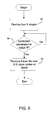
- FIG. 5 is a flow diagram illustrating a mode of operation involving restoration of a future file according to an embodiment of the invention.
- a pipeline may have a defined number of stages X ( 60 ). If an instruction is terminated in stage N ( 62 ), then the future file may be restored over a time period of X-N clock cycles or fewer ( 64 ). X-N clock cycles may be the time it takes to flush the pipeline.
- FIG. 6 is another flow diagram illustrating a mode of operation involving restoration of a future file according to an embodiment of the invention.
- a pipeline may have X stages ( 70 ), and an instruction may be terminated in stage N ( 72 ). At that point, the pipeline may finish executing instructions that are in an N+1 th stage or higher ( 74 ). Instructions in stage N or lower that implemented speculative registers in the future file may be identified ( 76 ), and the speculative registers associated with the identified instructions may be restored over more than one clock cycle. For instance, the speculative registers associated with the identified instructions may be restored over X-N clock cycles or fewer ( 78 ).
- the processor may be implemented in a variety of systems including general purpose computing systems, digital processing systems, laptop computers, personal digital assistants (PDA's) and cellular phones.
- the processor may be coupled to a memory device, such as a FLASH memory device or a static random access memory (SRAM) that stores an operating system and other software applications.
- a memory device such as a FLASH memory device or a static random access memory (SRAM) that stores an operating system and other software applications.
Abstract
Description
Claims (21)
Priority Applications (2)
| Application Number | Priority Date | Filing Date | Title |
|---|---|---|---|
| US09/823,276 US7124285B2 (en) | 2001-03-29 | 2001-03-29 | Peak power reduction when updating future file |
| TW091105736A TWI244029B (en) | 2001-03-29 | 2002-03-25 | Peak power reduction when updating future file |
Applications Claiming Priority (1)
| Application Number | Priority Date | Filing Date | Title |
|---|---|---|---|
| US09/823,276 US7124285B2 (en) | 2001-03-29 | 2001-03-29 | Peak power reduction when updating future file |
Publications (2)
| Publication Number | Publication Date |
|---|---|
| US20020144100A1 US20020144100A1 (en) | 2002-10-03 |
| US7124285B2 true US7124285B2 (en) | 2006-10-17 |
Family
ID=25238290
Family Applications (1)
| Application Number | Title | Priority Date | Filing Date |
|---|---|---|---|
| US09/823,276 Expired - Lifetime US7124285B2 (en) | 2001-03-29 | 2001-03-29 | Peak power reduction when updating future file |
Country Status (2)
| Country | Link |
|---|---|
| US (1) | US7124285B2 (en) |
| TW (1) | TWI244029B (en) |
Citations (13)
| Publication number | Priority date | Publication date | Assignee | Title |
|---|---|---|---|---|
| US5155817A (en) * | 1988-04-01 | 1992-10-13 | Kabushiki Kaisha Toshiba | Microprocessor |
| US5535346A (en) * | 1994-07-05 | 1996-07-09 | Motorola, Inc. | Data processor with future file with parallel update and method of operation |
| US5629698A (en) * | 1994-01-05 | 1997-05-13 | Texas Instruments Incorporated | Automatic offset tracking and correcting circuit and method of operation |
| US5654929A (en) * | 1995-09-14 | 1997-08-05 | Samsung Electronics Co., Ltd. | Refresh strategy for DRAMs |
| US5758112A (en) * | 1994-10-14 | 1998-05-26 | Silicon Graphics, Inc. | Pipeline processor with enhanced method and apparatus for restoring register-renaming information in the event of a branch misprediction |
| US5872951A (en) * | 1996-07-26 | 1999-02-16 | Advanced Micro Design, Inc. | Reorder buffer having a future file for storing speculative instruction execution results |
| US5915110A (en) * | 1996-07-26 | 1999-06-22 | Advanced Micro Devices, Inc. | Branch misprediction recovery in a reorder buffer having a future file |
| US6018798A (en) * | 1997-12-18 | 2000-01-25 | Advanced Micro Devices, Inc. | Floating point unit using a central window for storing instructions capable of executing multiple instructions in a single clock cycle |
| US6112310A (en) * | 1997-09-12 | 2000-08-29 | Samsung Electronics Co., Ltd. | Technique for generating memory clock in video controller |
| US6112296A (en) * | 1997-12-18 | 2000-08-29 | Advanced Micro Devices, Inc. | Floating point stack manipulation using a register map and speculative top of stack values |
| US6112018A (en) * | 1997-12-18 | 2000-08-29 | Advanced Micro Devices, Inc. | Apparatus for exchanging two stack registers |
| US6615343B1 (en) * | 2000-06-22 | 2003-09-02 | Sun Microsystems, Inc. | Mechanism for delivering precise exceptions in an out-of-order processor with speculative execution |
| US6898695B2 (en) * | 2001-03-28 | 2005-05-24 | Intel Corporation | Use of a future file for data address calculations in a pipelined processor |
-
2001
- 2001-03-29 US US09/823,276 patent/US7124285B2/en not_active Expired - Lifetime
-
2002
- 2002-03-25 TW TW091105736A patent/TWI244029B/en not_active IP Right Cessation
Patent Citations (14)
| Publication number | Priority date | Publication date | Assignee | Title |
|---|---|---|---|---|
| US5155817A (en) * | 1988-04-01 | 1992-10-13 | Kabushiki Kaisha Toshiba | Microprocessor |
| US5629698A (en) * | 1994-01-05 | 1997-05-13 | Texas Instruments Incorporated | Automatic offset tracking and correcting circuit and method of operation |
| US5535346A (en) * | 1994-07-05 | 1996-07-09 | Motorola, Inc. | Data processor with future file with parallel update and method of operation |
| US5758112A (en) * | 1994-10-14 | 1998-05-26 | Silicon Graphics, Inc. | Pipeline processor with enhanced method and apparatus for restoring register-renaming information in the event of a branch misprediction |
| US5654929A (en) * | 1995-09-14 | 1997-08-05 | Samsung Electronics Co., Ltd. | Refresh strategy for DRAMs |
| US5915110A (en) * | 1996-07-26 | 1999-06-22 | Advanced Micro Devices, Inc. | Branch misprediction recovery in a reorder buffer having a future file |
| US5872951A (en) * | 1996-07-26 | 1999-02-16 | Advanced Micro Design, Inc. | Reorder buffer having a future file for storing speculative instruction execution results |
| US6112310A (en) * | 1997-09-12 | 2000-08-29 | Samsung Electronics Co., Ltd. | Technique for generating memory clock in video controller |
| US6018798A (en) * | 1997-12-18 | 2000-01-25 | Advanced Micro Devices, Inc. | Floating point unit using a central window for storing instructions capable of executing multiple instructions in a single clock cycle |
| US6112296A (en) * | 1997-12-18 | 2000-08-29 | Advanced Micro Devices, Inc. | Floating point stack manipulation using a register map and speculative top of stack values |
| US6112018A (en) * | 1997-12-18 | 2000-08-29 | Advanced Micro Devices, Inc. | Apparatus for exchanging two stack registers |
| US6205541B1 (en) * | 1997-12-18 | 2001-03-20 | Advanced Micro Devices, Inc. | System and method using selection logic units to define stack orders |
| US6615343B1 (en) * | 2000-06-22 | 2003-09-02 | Sun Microsystems, Inc. | Mechanism for delivering precise exceptions in an out-of-order processor with speculative execution |
| US6898695B2 (en) * | 2001-03-28 | 2005-05-24 | Intel Corporation | Use of a future file for data address calculations in a pipelined processor |
Non-Patent Citations (4)
| Title |
|---|
| InstantWeb. "Free On-line Computing Dictionary". (C)1995. Search term: static randcom access memory http://www.instantweb.com/foldoc/foldoc.cgi?static+random+access+memory. * |
| Ozer et al., A Fast Interrupt Handling Scheme for VLIW Processors, Proceedings of the International Conference on Parallel Architectures and Compilation Techniques, Oct. 1998, p. 136-141. * |
| Smith et al., Implementing Precise Interrupts in Pipelined Processors, IEEE Transactions on Computers, May 1988, p. 562-573. * |
| Translation of Feb. 2, 2005 Office Action in Taiwan prosecution of Application No. 091105736. |
Also Published As
| Publication number | Publication date |
|---|---|
| US20020144100A1 (en) | 2002-10-03 |
| TWI244029B (en) | 2005-11-21 |
Similar Documents
| Publication | Publication Date | Title |
|---|---|---|
| US6823448B2 (en) | Exception handling using an exception pipeline in a pipelined processor | |
| US6115808A (en) | Method and apparatus for performing predicate hazard detection | |
| US7028165B2 (en) | Processor stalling | |
| US5574872A (en) | Method and apparatus for controlling the saving of pipelines in pipelined processors during trap handling | |
| US5761467A (en) | System for committing execution results when branch conditions coincide with predetermined commit conditions specified in the instruction field | |
| US6665795B1 (en) | Resetting a programmable processor | |
| US7472259B2 (en) | Multi-cycle instructions | |
| US6898693B1 (en) | Hardware loops | |
| US6748523B1 (en) | Hardware loops | |
| US7065636B2 (en) | Hardware loops and pipeline system using advanced generation of loop parameters | |
| US6070218A (en) | Interrupt capture and hold mechanism | |
| US6766444B1 (en) | Hardware loops | |
| US7269720B2 (en) | Dynamically controlling execution of operations within a multi-operation instruction | |
| US6721878B1 (en) | Low-latency interrupt handling during memory access delay periods in microprocessors | |
| US6920547B2 (en) | Register adjustment based on adjustment values determined at multiple stages within a pipeline of a processor | |
| US7124285B2 (en) | Peak power reduction when updating future file | |
| JPH07182165A (en) | Processing method/device for instruction with committing condition | |
| US6789187B2 (en) | Processor reset and instruction fetches | |
| US20050071830A1 (en) | Method and system for processing a sequence of instructions |
Legal Events
| Date | Code | Title | Description |
|---|---|---|---|
| AS | Assignment |
Owner name: INTEL CORPORATION, CALIFORNIA Free format text: ASSIGNMENT OF ASSIGNORS INTEREST;ASSIGNORS:INOUE, RYO;REVILLA, JUAN G.;REEL/FRAME:011976/0717;SIGNING DATES FROM 20010611 TO 20010619 Owner name: ANALOG DEVICES, INC., MASSACHUSETTS Free format text: ASSIGNMENT OF ASSIGNORS INTEREST;ASSIGNORS:INOUE, RYO;REVILLA, JUAN G.;REEL/FRAME:011976/0717;SIGNING DATES FROM 20010611 TO 20010619 |
|
| STCF | Information on status: patent grant |
Free format text: PATENTED CASE |
|
| AS | Assignment |
Owner name: ANALOG DEVICES, INC., MASSACHUSETTS Free format text: ASSIGNMENT OF ASSIGNORS INTEREST;ASSIGNOR:INTEL CORPORATION;REEL/FRAME:018891/0599 Effective date: 20061108 |
|
| FPAY | Fee payment |
Year of fee payment: 4 |
|
| FPAY | Fee payment |
Year of fee payment: 8 |
|
| MAFP | Maintenance fee payment |
Free format text: PAYMENT OF MAINTENANCE FEE, 12TH YEAR, LARGE ENTITY (ORIGINAL EVENT CODE: M1553) Year of fee payment: 12 |